WO2016199352A1 - 半導体装置 - Google Patents
半導体装置 Download PDFInfo
- Publication number
- WO2016199352A1 WO2016199352A1 PCT/JP2016/002357 JP2016002357W WO2016199352A1 WO 2016199352 A1 WO2016199352 A1 WO 2016199352A1 JP 2016002357 W JP2016002357 W JP 2016002357W WO 2016199352 A1 WO2016199352 A1 WO 2016199352A1
- Authority
- WO
- WIPO (PCT)
- Prior art keywords
- fin
- semiconductor
- refrigerant
- semiconductor device
- portions
- Prior art date
Links
- 239000004065 semiconductor Substances 0.000 title claims abstract description 195
- 239000003507 refrigerant Substances 0.000 claims abstract description 119
- 239000011347 resin Substances 0.000 claims abstract description 37
- 229920005989 resin Polymers 0.000 claims abstract description 37
- 238000001816 cooling Methods 0.000 claims description 44
- 230000001154 acute effect Effects 0.000 claims description 14
- 238000011144 upstream manufacturing Methods 0.000 claims description 10
- 230000005855 radiation Effects 0.000 claims description 5
- 230000015572 biosynthetic process Effects 0.000 claims description 2
- 230000017525 heat dissipation Effects 0.000 abstract description 19
- 239000012071 phase Substances 0.000 description 33
- 238000012546 transfer Methods 0.000 description 21
- 239000002826 coolant Substances 0.000 description 15
- 239000000463 material Substances 0.000 description 15
- 238000010586 diagram Methods 0.000 description 12
- 239000012530 fluid Substances 0.000 description 12
- 239000004020 conductor Substances 0.000 description 9
- 239000003990 capacitor Substances 0.000 description 8
- 238000004088 simulation Methods 0.000 description 8
- 230000007423 decrease Effects 0.000 description 7
- 230000000694 effects Effects 0.000 description 5
- 230000020169 heat generation Effects 0.000 description 5
- 229910000679 solder Inorganic materials 0.000 description 5
- 238000013210 evaluation model Methods 0.000 description 4
- 239000010410 layer Substances 0.000 description 4
- 238000004519 manufacturing process Methods 0.000 description 4
- 238000012986 modification Methods 0.000 description 4
- 230000004048 modification Effects 0.000 description 4
- 210000001015 abdomen Anatomy 0.000 description 3
- 229910052802 copper Inorganic materials 0.000 description 3
- 238000009499 grossing Methods 0.000 description 3
- 238000010438 heat treatment Methods 0.000 description 3
- 239000011810 insulating material Substances 0.000 description 3
- 238000012545 processing Methods 0.000 description 3
- 238000007789 sealing Methods 0.000 description 3
- 239000000758 substrate Substances 0.000 description 3
- 239000003985 ceramic capacitor Substances 0.000 description 2
- 238000011156 evaluation Methods 0.000 description 2
- 238000003384 imaging method Methods 0.000 description 2
- 238000009413 insulation Methods 0.000 description 2
- 238000000465 moulding Methods 0.000 description 2
- XLYOFNOQVPJJNP-UHFFFAOYSA-N water Substances O XLYOFNOQVPJJNP-UHFFFAOYSA-N 0.000 description 2
- 229910018072 Al 2 O 3 Inorganic materials 0.000 description 1
- 239000004593 Epoxy Substances 0.000 description 1
- 239000000853 adhesive Substances 0.000 description 1
- 230000001070 adhesive effect Effects 0.000 description 1
- JRPBQTZRNDNNOP-UHFFFAOYSA-N barium titanate Chemical compound [Ba+2].[Ba+2].[O-][Ti]([O-])([O-])[O-] JRPBQTZRNDNNOP-UHFFFAOYSA-N 0.000 description 1
- 229910002113 barium titanate Inorganic materials 0.000 description 1
- 239000000919 ceramic Substances 0.000 description 1
- 239000012141 concentrate Substances 0.000 description 1
- 230000006866 deterioration Effects 0.000 description 1
- 230000005489 elastic deformation Effects 0.000 description 1
- 230000006872 improvement Effects 0.000 description 1
- 230000006698 induction Effects 0.000 description 1
- 238000003780 insertion Methods 0.000 description 1
- 230000037431 insertion Effects 0.000 description 1
- 239000012212 insulator Substances 0.000 description 1
- 239000007791 liquid phase Substances 0.000 description 1
- 229910052751 metal Inorganic materials 0.000 description 1
- 239000002184 metal Substances 0.000 description 1
- 238000000034 method Methods 0.000 description 1
- 229920001296 polysiloxane Polymers 0.000 description 1
- 230000008569 process Effects 0.000 description 1
- 230000009467 reduction Effects 0.000 description 1
- 238000010992 reflux Methods 0.000 description 1
- 125000006850 spacer group Chemical group 0.000 description 1
- 239000002344 surface layer Substances 0.000 description 1
Images


Classifications
-
- H—ELECTRICITY
- H01—ELECTRIC ELEMENTS
- H01L—SEMICONDUCTOR DEVICES NOT COVERED BY CLASS H10
- H01L23/00—Details of semiconductor or other solid state devices
- H01L23/34—Arrangements for cooling, heating, ventilating or temperature compensation ; Temperature sensing arrangements
- H01L23/46—Arrangements for cooling, heating, ventilating or temperature compensation ; Temperature sensing arrangements involving the transfer of heat by flowing fluids
- H01L23/473—Arrangements for cooling, heating, ventilating or temperature compensation ; Temperature sensing arrangements involving the transfer of heat by flowing fluids by flowing liquids
-
- F—MECHANICAL ENGINEERING; LIGHTING; HEATING; WEAPONS; BLASTING
- F28—HEAT EXCHANGE IN GENERAL
- F28F—DETAILS OF HEAT-EXCHANGE AND HEAT-TRANSFER APPARATUS, OF GENERAL APPLICATION
- F28F3/00—Plate-like or laminated elements; Assemblies of plate-like or laminated elements
- F28F3/02—Elements or assemblies thereof with means for increasing heat-transfer area, e.g. with fins, with recesses, with corrugations
- F28F3/022—Elements or assemblies thereof with means for increasing heat-transfer area, e.g. with fins, with recesses, with corrugations the means being wires or pins
-
- H—ELECTRICITY
- H01—ELECTRIC ELEMENTS
- H01L—SEMICONDUCTOR DEVICES NOT COVERED BY CLASS H10
- H01L21/00—Processes or apparatus adapted for the manufacture or treatment of semiconductor or solid state devices or of parts thereof
- H01L21/02—Manufacture or treatment of semiconductor devices or of parts thereof
- H01L21/04—Manufacture or treatment of semiconductor devices or of parts thereof the devices having potential barriers, e.g. a PN junction, depletion layer or carrier concentration layer
- H01L21/48—Manufacture or treatment of parts, e.g. containers, prior to assembly of the devices, using processes not provided for in a single one of the subgroups H01L21/06 - H01L21/326
- H01L21/4814—Conductive parts
- H01L21/4871—Bases, plates or heatsinks
- H01L21/4878—Mechanical treatment, e.g. deforming
-
- F—MECHANICAL ENGINEERING; LIGHTING; HEATING; WEAPONS; BLASTING
- F28—HEAT EXCHANGE IN GENERAL
- F28F—DETAILS OF HEAT-EXCHANGE AND HEAT-TRANSFER APPARATUS, OF GENERAL APPLICATION
- F28F3/00—Plate-like or laminated elements; Assemblies of plate-like or laminated elements
- F28F3/12—Elements constructed in the shape of a hollow panel, e.g. with channels
-
- H—ELECTRICITY
- H01—ELECTRIC ELEMENTS
- H01L—SEMICONDUCTOR DEVICES NOT COVERED BY CLASS H10
- H01L2224/00—Indexing scheme for arrangements for connecting or disconnecting semiconductor or solid-state bodies and methods related thereto as covered by H01L24/00
- H01L2224/01—Means for bonding being attached to, or being formed on, the surface to be connected, e.g. chip-to-package, die-attach, "first-level" interconnects; Manufacturing methods related thereto
- H01L2224/02—Bonding areas; Manufacturing methods related thereto
- H01L2224/04—Structure, shape, material or disposition of the bonding areas prior to the connecting process
- H01L2224/06—Structure, shape, material or disposition of the bonding areas prior to the connecting process of a plurality of bonding areas
- H01L2224/0601—Structure
- H01L2224/0603—Bonding areas having different sizes, e.g. different heights or widths
-
- H—ELECTRICITY
- H01—ELECTRIC ELEMENTS
- H01L—SEMICONDUCTOR DEVICES NOT COVERED BY CLASS H10
- H01L23/00—Details of semiconductor or other solid state devices
- H01L23/34—Arrangements for cooling, heating, ventilating or temperature compensation ; Temperature sensing arrangements
- H01L23/36—Selection of materials, or shaping, to facilitate cooling or heating, e.g. heatsinks
- H01L23/367—Cooling facilitated by shape of device
- H01L23/3677—Wire-like or pin-like cooling fins or heat sinks
Definitions
- the present disclosure relates to a semiconductor device having a structure in which a semiconductor module provided with a heating element is cooled by a cooler.
- the thermal resistance Rth is expressed by the following equation, where ⁇ Tj is the heat generation temperature of the power element serving as the heat generation element and P is the heat generation amount.
- a desired output for example, 100 Arms
- an increase in the chip area constituting the power element and an increase in cost are caused. That is, since the cost increases as the thermal resistance increases, it is important to increase the heat dissipation efficiency to lower the element heat generation temperature and reduce the element size.
- the semiconductor module in order to increase the heat dissipation efficiency of the semiconductor module, the semiconductor module is provided with a heat radiating plate in which fin portions are formed, and a cooler is disposed so as to cover the fin portions. Heat dissipation of the semiconductor module is promoted by allowing the coolant to flow in the internal space of the cooler, and heat dissipation efficiency is further increased by providing the semiconductor module with a heat dissipation plate.
- a fin part is comprised by digging up with the digging tool which has a linear or broken line-shaped blade part, and is set as the structure by which the linear form or plurality is arrange
- a cylindrical portion having a heat radiating plate in which a plurality of cylindrical straight fins are formed is inserted from an opening portion of the cooling base constituting the refrigerant passage, and the cooling base is provided at a flange portion provided at the rear end of the cylindrical portion in the insertion direction.
- the cylinder portion is fixed to the base.
- a seal member is provided between the flange portion and the cooling base, and the opening portion of the cooling base is sealed by the flange portion and the seal member. Then, when the refrigerant is caused to flow through the refrigerant passage formed in the cooling base, the refrigerant flows so as to collide with the straight fins. Thereby, high heat dissipation efficiency is obtained.
- the heat transfer surface is expanded by taking a large surface area, so that it is perpendicular to the direction in which the fin portion is dug up.
- the direction is the refrigerant flow direction. That is, fins formed in a straight line shape or a broken line shape are arranged in a plurality of rows in parallel, and the refrigerant flows so as to pass between the plurality of rows of fin portions. Since the refrigerant flow becomes uniform in this way, it is difficult to increase the cooling efficiency.
- the tip of the straight fin and the inner wall surface of the refrigerant passage are arranged so that the cylindrical portion can be inserted into the refrigerant passage of the cooling base It is necessary to provide a gap between the two. Since the refrigerant passes through this gap as a bypass passage without passing through the fin portion, the heat transfer rate is lowered and the heat radiation efficiency is lowered. In addition, since straight fins are formed by molding or the like, and the surface of the heat sink is not a flat surface from the beginning, it is difficult to inspect the bonding state of the element portion with an ultrasonic imaging device (SAT) or the like.
- SAT ultrasonic imaging device
- the present disclosure provides a semiconductor device capable of making a surface flat before digging up and cooling a semiconductor module with higher cooling efficiency by using a fin portion formed by digging up.
- the purpose is to do.
- a semiconductor device is exposed to a semiconductor element that serves as a heating element, a plate-shaped resin mold portion that covers the semiconductor element, and the resin mold portion, and is exposed from one surface of the resin mold portion.
- at least one semiconductor module having a heat radiating plate that radiates heat generated by the semiconductor element while being insulated from the semiconductor element, and the heat radiating plate in the semiconductor module is exposed on one surface.
- a cooler that constitutes a refrigerant passage and promotes heat radiation from the heat radiating plate by flowing the refrigerant into the refrigerant passage.
- the heat radiating plate is provided with fin portions formed by digging up the surface of the heat radiating plate.
- the fin portion is tapered and has an elliptical arc shape that is curved from the root portion to the tip portion.
- the fin portion is formed by digging and the fin portion has an elliptical arc shape. And since the fin part is made into elliptical arc shape, the flow of the refrigerant
- FIG. 1 is a circuit diagram of a three-phase inverter circuit configured by a semiconductor module included in the semiconductor device according to the first embodiment of the present disclosure.
- FIG. 2 is a perspective view of the semiconductor module
- FIG. 3 is a perspective view showing a state in which both sides of the semiconductor module are sandwiched between cooling devices
- FIG. 4 is an exploded perspective view of the components of the semiconductor module
- FIG. 5 is a top layout view of the semiconductor module.
- FIG. 6 is a perspective view of a multilayer wiring bus bar
- FIG. 7 is a cross-sectional view of the semiconductor device
- FIG. 8 is an exploded view of the semiconductor device
- FIG. 1 is a circuit diagram of a three-phase inverter circuit configured by a semiconductor module included in the semiconductor device according to the first embodiment of the present disclosure.
- FIG. 2 is a perspective view of the semiconductor module
- FIG. 3 is a perspective view showing a state in which both sides of the semiconductor module are sandwiched between cooling devices
- FIG. 4
- FIG. 9 is a top view of the semiconductor module
- FIG. 10 is a cross-sectional view of the vicinity of the fin portion
- FIG. 11 is a top view of the fin portion
- FIG. 12 is a diagram showing the result of simulating the relationship between the gap at the top of the fin portion and the bypass flow rate ratio
- FIG. 13A is a top surface layout diagram of the model used in the simulation of FIG.
- FIG. 13B is a cross-sectional view of the model used in the simulation of FIG.
- FIG. 14 is a diagram showing the relationship of the deformation amount to the applied load
- FIG. 15A is a cross-sectional view of the model used in the simulation of FIG.
- FIG. 15B is a cross-sectional view of the model used in the simulation of FIG. FIG.
- FIG. 16 is a cross-sectional view of a model of an elliptic arc fin
- FIG. 17 is a diagram showing the relationship between the coefficient k and the heat transfer coefficient / pressure loss ratio.
- FIG. 18 is a diagram showing the relationship between the fluid vector and the heat transfer coefficient / pressure loss ratio.
- FIG. 19 is a diagram showing the relationship between the normalized pressure loss and the normalized heat transfer coefficient
- FIG. 20 is a cross-sectional view of a model used for comparison of cooling performance.
- FIG. 21 is a flow velocity contour diagram in the recess
- FIG. 22 is a diagram showing the results of examining the cooling efficiency for each structure when straight fins are used as a reference.
- FIG. 21 is a flow velocity contour diagram in the recess
- FIG. 22 is a diagram showing the results of examining the cooling efficiency for each structure when straight fins are used as a reference.
- FIG. 21 is a flow velocity contour diagram in the recess
- FIG. 22 is a diagram showing the
- FIG. 23 is a diagram showing the relationship between the direction of the refrigerant flow and the direction in which the fins are dug up
- FIG. 24 is a cross-sectional view of the fin portion according to the second embodiment of the present disclosure
- FIG. 25 (a) is a side view of the digging tool
- FIG. 25 (b) is a front view of the digging tool
- FIG.25 (c) is sectional drawing of the fin part dug up by the dug-up tool
- FIG. 26 is a top view of the fin portion according to the third embodiment of the present disclosure
- FIG. 27 is a front view of a digging tool used for forming the fin portion shown in FIG.
- FIG. 28 is a top view of a fin portion according to a modification of the third embodiment
- FIG. 29 is a front view of a digging tool used for forming the fin portion shown in FIG.
- FIG. 30 is a perspective view of a semiconductor device according to the fourth embodiment of the present disclosure.
- FIG. 31 is an exploded view of the semiconductor device shown in FIG.
- FIG. 32 is a cross-sectional view of the fin portions of two semiconductor modules
- FIG. 33 is a perspective view of an inverter unit to which a semiconductor device in which a plurality of semiconductor modules are stacked is applied.
- the configuration of the three-phase inverter circuit 1 provided in the semiconductor module will be described with reference to FIG.
- the three-phase inverter circuit 1 is for driving a load 3 such as a three-phase AC motor based on a DC power source (external power source) 2.
- a smoothing capacitor 4 is connected in parallel to the three-phase inverter circuit 1 so that a constant power supply voltage can be formed by suppressing ripple reduction during switching and the influence of noise.
- the three-phase inverter circuit 1 has a configuration in which upper and lower arms 51 to 56 connected in series are connected in parallel for three phases, and an intermediate potential between the upper arms 51, 53, 55 and the lower arms 52, 54, 56 is applied to the load 3
- the three-phase AC motor to be applied is applied while sequentially switching to the U phase, V phase, and W phase.
- the upper and lower arms 51 to 56 are respectively provided with semiconductor switching elements 51a to 56a such as IGBTs and MOSFETs serving as heating elements and rectifier elements (one-side conduction elements) 51b to 56b for the purpose of reflux such as FWD.
- the semiconductor switching elements 51a to 56a of the upper and lower arms 51 to 56 of each phase are on / off controlled, so that three-phase alternating currents having different cycles are supplied to the three-phase alternating current motor. As a result, the three-phase AC motor can be driven.
- the semiconductor chips on which the semiconductor switching elements 51a to 51f and the rectifying elements 51b to 56b constituting the six upper and lower arms 51 to 56 provided in the three-phase inverter circuit 1 are formed as a module and integrated.
- the three-phase inverter circuit 1 is configured as a 6-in-1 semiconductor module in which six arms are integrated.
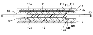
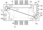
- the semiconductor module 6 shown in FIG. 2 includes a semiconductor chip 10, upper and lower radiator plates 11, 12, a multilayer wiring bus bar 13 in which various terminals and wires are integrated, a control terminal 14, and an element relay electrode. 15 and plates 16, 17 and the like. Of these, six sets of component blocks are provided, with the semiconductor chip 10, the control terminal 14, the element relay electrode 15, the plates 16, 17, etc. as component blocks for one arm. Then, six sets of component parts blocks are sandwiched between the upper and lower radiator plates 11 and 12 together with the multilayer wiring bus bar 13 and covered with a resin mold portion 18 as shown in FIG. Thus, the semiconductor module 6 is configured as a plate-like member having a predetermined thickness as shown in FIG.
- Such a semiconductor module 6 is used to drive the load 3 while dissipating heat by sandwiching both sides in the thickness direction by a cooler 19 as shown in FIG.
- a cooler 19 as shown in FIG.
- through holes 19a are provided at two opposite corners of each cooler 19, and a passage constituting portion 19d that constitutes a refrigerant passage by connecting each through hole 10a is provided. Thereby, the cooling of the cooler 19 is performed, so that the semiconductor module 6 is used while enabling efficient cooling.
- the semiconductor chip 10 shown in FIG. 4 is composed of six chips 10a to 10f.
- Each of the chips 10a to 10f has a front surface and a back surface, and semiconductor switching elements 51a to 56a, rectifying elements 51b to 56b, and the like constituting the upper arms 51, 53, 55 or the lower arms 52, 54, 56, respectively, are formed.
- the semiconductor chip 10 is formed using a semiconductor substrate such as Si, SiC, or GaN as a base material substrate.
- the semiconductor switching elements 51a to 56a and the rectifying elements 51b to 56b formed in the semiconductor chip 10 are vertical elements that allow current to flow in the direction perpendicular to the substrate, and various electrodes are provided on the front and back sides of the semiconductor chip 10.
- each semiconductor chip 10 is electrically and physically connected to the surface side of the lower plate 17 via a bonding material 20 made of a high thermal conductive material such as solder or Ag sintered material. It is connected to the. And the back surface side of the lower plate 17 is joined to the lower heat radiating plate 12 via a joining material 21 made of a high thermal conductive material such as solder or Ag sintered material.
- the surface side of the semiconductor chip 10 is a bonding material 22 made of a high thermal conductive material such as solder or Ag sintered material with respect to the element relay electrode 15 made of Cu, Al, Fe or the like as a base material. Connected through. Furthermore, the element relay electrode 15 is electrically and physically connected to the back surface side of the upper plate 16 through a bonding material 23 made of a high thermal conductive material such as solder or Ag sintered material. And the surface side of the upper side plate 16 is joined to the upper side heat sink 11 via the joining material 24 comprised with the high heat conductive material like a solder or Ag sintered material.
- each semiconductor chip 10 is sandwiched between the upper and lower radiator plates 11 and 12.
- the semiconductor chip 10 is configured such that elements such as the semiconductor switching elements 51a to 56a and the rectifying elements 51b to 56b constituting the arms 51 to 56 are formed together in one chip.
- elements such as semiconductor switching elements 51a to 56a and rectifying elements 51b to 56b constituting the arms 51 to 56 may be formed on separate chips.
- the upper and lower heat sinks 11 and 12 correspond to heat sinks, and are composed of, for example, a high thermal conductive member mainly composed of Cu, Al, Fe, etc., one surface side facing the semiconductor chip 10 and the other surface side shown in FIG. 2, the resin mold portion 18 is exposed.
- the upper and lower heat radiating plates 11 and 12 are stepped, and the inner side portions 11b and 12b (see FIG. 7) that are inside the outer edge portions 11a and 12a (see FIG. 7). Is projected by a predetermined amount.
- the outer edge portions 11 a and 12 a are flush with one surface of the resin mold portion 18 around the outer edge portions 11 a and 12 a, and the inner portions 11 b and 12 b protrude from the resin mold portion 18 by a predetermined distance.
- the inner portions 11b and 12b are formed with a plurality of fin portions 11c and 12c formed by digging up the surface layer portions of the inner portions 11b and 12b and using a tool. The detailed structure of the plurality of fin portions 11c and 12c will be described later. In FIG. 7, each component provided in the resin mold portion 18 is omitted from illustration.
- the upper and lower radiator plates 11 and 12 are in an insulated state from the semiconductor chip 10 because the upper and lower plates 16 and 17 are partially made of an insulating material.
- the upper and lower plates 16 and 17 and the element relay electrode 15 are made of a highly heat conductive material, the upper and lower heat sinks 11 and 12 have high heat conduction from the semiconductor chip 10. It is reported in. Then, heat can be radiated from the front surface side of the upper heat radiating plate 11 and the back surface side of the lower heat radiating plate 12, that is, the surface on which the fin portions 11c and 12c are formed.
- the multilayer wiring bus bar 13 is a part constituting various wirings and various terminals in the semiconductor module 6 of the present embodiment.
- the multilayer wiring bus bar 13 is composed of a plate-like bar-like member, and includes the semiconductor chip 10 that constitutes the upper arms 51, 53, and 55 of each phase and the semiconductor chip 10 that constitutes the lower arms 52, 54, and 56. It is arranged to pass between.
- the positive side wiring connecting the upper arms 51, 53, 55 and the + terminal of the DC power source 2 and the negative electrode connecting the lower arms 52, 54, 56 and the ⁇ terminal of the DC power source 2.
- Side wiring and output wiring for connecting the arms 51 to 56 and the load 3 are provided.
- the multilayer wiring bus bar 13 is provided with various connection terminals 13a to 13e for connecting each wiring to the DC power source 2 and the load 3.
- the multilayer wiring bus bar 13 is configured by a plate-like bar-shaped member having one direction as a longitudinal direction, and one end side and the other end side are substantially square as shown in FIG. 2. It is exposed from the two opposite sides of the resin mold part 18 having a shape.
- the positive terminal 13 a that connects the upper arms 51, 53, 55 and the positive terminal of the DC power source 2, the lower arms 52, 54, 56 and the DC power source 2
- a negative terminal 13b is formed to connect the negative terminal.
- a U terminal 13c corresponding to an output terminal for connecting the intermediate potential point of the upper and lower arms 51 to 56 and the load 3 in each phase of the U phase, V phase, and W phase.
- a V terminal 13d and a W terminal 13e are exposed from the resin mold 18 as shown in FIG.
- the semiconductor module 6 and the DC power source 2 and the smoothing capacitor 4 are electrically connected via the positive terminal 13a and the negative terminal 13b.
- electrical connection with the U-phase, V-phase, and W-phase of the three-phase AC motor serving as the load 3 is performed via the U terminal 13c, the V terminal 13d, and the W terminal 13e.
- Such a multilayer wiring bus bar 13 is configured by a multilayer wiring structure in which patterned conductor layers and insulating layers are laminated, and circuit wiring for electrically connecting each part of the three-phase inverter circuit 1 shown in FIG. Is configured.
- the pads 136a to 136c and 139a to 139c provided in the multilayer wiring bus bar 13 are electrically connected to predetermined portions of the semiconductor chips 10a to 10f.
- a plurality of pads electrically connected to predetermined portions of the semiconductor chips 10a to 10f are also provided on the surface of the multilayer wiring bus bar 13 opposite to the surface on which the pads 136a to 136c and 139a to 139c are disposed. Is provided.
- the internal wiring provided in the multilayer wiring bus bar 13 and the pads 136a to 136c, 139a to 139c are electrically connected, and the internal wiring and the terminals 13a to 13e are electrically connected to each other, so that the three-phase inverter
- the wiring structure of the circuit 1 is configured.
- the internal wiring is covered with an insulating film 130, and pads 136a to 136c, 139a to 139c and terminals 13a to 13e are provided so as to be exposed from the insulating film 130.
- the control terminal 14 serves as a signal line terminal constituting various signal lines such as gate wirings of the semiconductor switching elements 51a to 56a.
- the control terminal 14 is electrically connected to the electrodes connected to the gates of the semiconductor switching elements 51a to 56a formed on the surface side of the semiconductor chip 10 via bonding wires 25 (see FIG. 4) made of Au or the like. It is connected to the.
- the end portion of the control terminal 14 opposite to the semiconductor chip 10 is exposed from the resin mold portion 18 as shown in FIG. 2, and is configured to be connected to the outside through this exposed portion.
- the control terminal 14 is described as being integrated in a lead frame state, and is also integrated with the lower heat sink 12.
- the signal lines are divided, and each signal line becomes independent.
- the element relay electrode 15 is a member that is electrically connected to the upper plate 16 while being electrically connected to the electrode on the surface of the semiconductor chip 10 on one surface of the semiconductor chip 10 side.
- the element relay electrode 15 is provided in order to provide a gap between the semiconductor chip 10 and the upper plate 16 by an amount corresponding to the bonding wire 25 disposed.
- the element relay electrode 15 is composed of a high heat conductive member mainly composed of Cu or the like, for example.
- the upper plate 16 serves to insulate the semiconductor chip 10 and the upper heat dissipation plate 11 from each other on the one surface of the semiconductor chip 10 while electrically connecting to the surface electrode of the semiconductor chip 10 via the element relay electrode 15. Fulfill.
- the lower plate 17 serves to insulate the semiconductor chip 10 and the lower heat dissipation plate 12 while making electrical connection with the electrode on the back surface of the semiconductor chip 10 on one surface of the semiconductor chip 10 side.
- the upper and lower plates 16 and 17 on the side of the semiconductor chip 10 is constituted by a high heat conductive member whose base material is Cu, Al or the like so that thermal conductivity is enhanced in addition to electrical connection.
- the layer located on the opposite side of the semiconductor chip 10 side from the one surface on the semiconductor chip 10 side is made of, for example, inorganic or organic so as to increase the thermal conductivity while achieving insulation. It is made of an insulating material.
- the upper and lower plates 16 and 17 can be configured by bonding a conductive plate having Cu as a base material on both surfaces of a ceramic insulator such as Si 3 N 4 , AlN, or Al 2 O 3 .
- the upper and lower plates 16 and 17 may be configured by bonding a Cu plate having an insulating sheet attached thereto and an adhesive sheet having an insulating adhesion function to a die bond plate made of a conductor member such as Cu. it can.
- the upper plate 16 has the surface electrodes of the semiconductor switching elements 51a to 56a (for example, the source of the MOSFET and the emitter of the IGBT) and the first electrodes of the rectifying elements 51b to 56b (for example, the anode such as FWD). ).
- the upper plate 16 is also electrically connected to the pads 136a to 136c and 139a to 139c provided on the multilayer wiring bus bar 13.
- the lower plate 17 is connected to the back electrodes of the semiconductor switching elements 51a to 56a (for example, the drain of the MOSFET and the collector of the IGBT) and the second electrodes of the rectifying elements 51b to 56b (for example, the cathode such as FWD).
- the lower plate 17 is also electrically connected to each pad (not shown) provided on the back side of the multilayer wiring bus bar 13. For this reason, the upper and lower plates 16 and 17 constitute part of the positive electrode side wiring, the negative electrode side wiring, and the output wiring for each of the arms 51 to 56.
- both the surface side of the upper heat radiating plate 11 and the back surface side of the lower heat radiating plate 12, that is, the surface opposite to the surface on which the semiconductor chip 10 is disposed are both from the resin mold portion 18. It is exposed, and heat can be radiated in this exposed portion.
- a cooler 19 is disposed on the heat radiation surface side. As shown in FIG. 7, the cooler 19 has a flow passage 19b formed by a cavity formed therein, and the refrigerant can flow through the flow passage 19b. For this reason, the heat radiating surfaces of the upper and lower heat radiating plates 11 and 12 come into contact with the refrigerant.
- the insulation between the semiconductor chip 10 and the upper and lower heat sinks 11 and 12 is achieved by the upper and lower plates 16 and 17, the current flows to the outside through the upper and lower heat sinks 11 and 12. Leakage can be prevented from occurring.
- the resin mold portion 18 is a sealing resin configured by placing each of the above-described components in a mold and then encapsulating the resin in the mold, and is configured, for example, in a rectangular plate shape.
- the resin mold part 18 is made of an insulating resin having a lower linear expansion coefficient and Young's modulus than the conductor parts such as the upper and lower radiator plates 11 and 12.
- the resin mold portion 18 can be mainly composed of an organic resin such as epoxy or silicone. From the resin mold portion 18, the front end of the control terminal 14 and both ends of the multilayer wiring bus bar 13 are exposed from each side constituting the quadrangular plate shape, and can be electrically connected to the outside.
- control terminals 14 of the upper arms 51, 53, and 55 and the lower arm 52 from opposite two sides of the resin mold portion 18 that is formed in a rectangular plate shape, that is, in the opposite direction across the resin mold portion 18,
- the control terminals 14 of 54 and 56 are exposed.
- both ends of the multilayer wiring bus bar 13 are exposed from two opposite sides of the resin mold portion 18 having a rectangular plate shape, that is, in opposite directions across the resin mold portion 18.
- the upper heat radiating plate 11 and the lower heat radiating plate 12 are exposed from the front and back surfaces of the rectangular plate shape, respectively, so that heat can be radiated satisfactorily.
- the above-described parts are mounted on the surface side of the lower heat sink 12 in the lead frame state in which the control terminals 14 are integrated. Then, after the electrical connection between the semiconductor chip 10 and the control terminal 14 is completed with the bonding wires 25, the upper heat radiating plate 11 and the like are mounted thereon. In this state, these are placed in a mold, and a resin mold portion 18 is formed by injecting resin into the mold and molding it. In addition to the surfaces of the upper and lower heat sinks 11 and 12, the resin mold portion 18 covers other than the exposed portions of the control terminal 14 and the multilayer wiring bus bar 13, thereby protecting the semiconductor chip 10 and the like.
- the cooler 19 includes a refrigerant passage 19b therein, and promotes heat dissipation of the semiconductor module 6 by allowing the refrigerant to flow.
- the cooler 19 is disposed on both heat radiation surfaces of the semiconductor module 6 where the upper and lower heat sinks 11 and 12 are disposed, and the cooler 19 and the semiconductor module 6 are stacked so as to sandwich the semiconductor module 6 by the cooler 19. ing. Then, as shown in FIG. 8, the cooler 19 and the semiconductor module 6 are fastened with bolts 28 while the semiconductor module 6 is sandwiched between the two coolers 19.
- the cooler 19 includes a hollow plate-like portion 19c having a substantially rectangular shape when viewed from the side opposite to the semiconductor module 6 and a passage constituting portion in which a through hole 19a is formed. 19d.
- the hollow portion configured in the hollow plate-like portion 19c as the refrigerant passage 10b With the hollow portion configured in the hollow plate-like portion 19c as the refrigerant passage 10b, the refrigerant introduced from one through hole 19a passes through the refrigerant passage 19b and is then discharged from the other through hole 19a.
- an opening 19e connected to the refrigerant passage 19b is formed on one surface of the hollow plate-like portion 19c on the semiconductor module 6 side.
- Inner portions 11b and 12b and fin portions 11c and 12c are arranged in the opening 19e.
- the outer edge shape of the inner side portions 11b and 12b and the shape of the opening portion 19e are matched, and the cooler 19 is assembled to the semiconductor module 6 so that the inner side portions 11b and 12b are fitted into the opening portion 19e.
- One surface of the hollow plate-like portion 19c on the side of the semiconductor module 6 has a structure having a predetermined thickness, and the thickness is made to match the protruding amount from the outer edge portions 11a and 12a of the inner portions 11b and 12b. .
- a seal member 26 surrounding the opening 19 e is disposed between the cooler 19 and the semiconductor module 6. For this reason, the space between the cooler 19 and the semiconductor module 6 is sealed by the sealing member 26 to prevent refrigerant leakage.
- the dimension of the refrigerant passage 19b formed in the cooler 19 is smaller than the height of the fin portions 11c and 12c.
- the tips of the fin portions 11c and 12c are tapered to facilitate deformation. For this reason, when the semiconductor module 6 and the cooler 19 are assembled, the fin portions 11c and 12c are brought into contact with the inner wall surfaces of the cooler 19 constituting the refrigerant passage 19b and the tips of the fin portions 11c and 12c are in contact with each other. When contacted, the tips of the fin portions 11c and 12c are deformed. As a result, the seal portion 26 is disposed without a gap between the cooler 19 and the semiconductor module 6 so that the seal function can be exhibited accurately.
- the passage constituting portion 19d has a rectangular shape, and a through hole 19a is formed at the center position thereof.
- the passage constituting portions 19d of the adjacent coolers 19 are in close contact with each other via a seal member 27 surrounding the through hole 19a, and the through holes 19a are connected to each other.
- the through hole 19a communicates with the refrigerant passage 19b. For this reason, the refrigerant introduced from the through hole 19a of one passage component 19d brought into close contact with each other passes through the refrigerant passage 10b and discharged from the through hole 19a of the other passage component 19d brought into close contact with each other. Is done.
- the dimension of the refrigerant passage 19b formed in the cooler 19 is smaller than the height of the fin portions 11c and 12c.
- the tip position of 12c is easily deformed.
- sticker part 26 is arrange
- path structure part 19d are arrange
- the end of the multilayer wiring bus bar 13 on the side where the positive and negative terminals 13a and 13b are arranged and the end on the side where the U to W terminals 13c to 13e are arranged are substantially rectangular. It arrange
- FIG. A through hole 19a is disposed at a position shifted from each of the terminals 13a to 13e. Therefore, the terminals 13a to 13e can be electrically connected to the external wiring without being hidden by the through hole 19a and the passage component 19d in the cooler 19.
- a semiconductor device having the semiconductor module 6 according to the present embodiment is configured by the structure as described above. Next, the detailed structure of the plurality of fin portions 11c and 12c formed on the heat radiating plates 11 and 12 will be described with reference to FIGS. 2, 7 and 9 to 11. FIG. In addition, although the several fin part 11c is mainly demonstrated here, the several fin part 12c is also set as the structure similar to the several fin part 11c.
- the inner portion 11b has a rectangular shape having a long side in the same direction as the longitudinal direction of the multilayer wiring bus bar 13 and a short side in the direction perpendicular thereto.
- the long side direction of the inner portion 11b is the x direction
- the short side direction is the y direction
- the normal direction of the inner portion 11b is the z direction
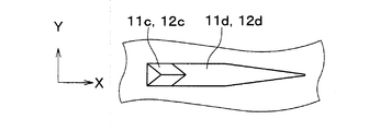
- the plurality of fin portions 11c are in the x direction and the y direction.
- each one of the several fin part 11c is comprised by digging up the surface of the inner side part 11b, and digging up in the z-axis direction with a tool.
- a plurality of rows arranged at equal intervals in the y direction are arranged at equal intervals in the x direction.
- column is shifted, and the layout which each fin part 11c of each row
- the refrigerant flow direction in the cooler 19 is a direction from the through hole 19a on the refrigerant introduction side to the through hole 19a on the refrigerant discharge side, and is indicated by an arrow A1 in the figure.
- the plurality of fin portions 11c arranged in a staggered arrangement are arranged along the refrigerant flow direction.
- the plurality of fin portions 11c being arranged along the refrigerant flow direction may mean that the plurality of fin portions 11c do not have to be parallel to the refrigerant flow direction, and the arrangement direction and the refrigerant flow direction. And may be angled.
- the plurality of fin portions 11c are formed by digging up the surface of the inner portion 11b along the y direction. For this reason, the coolant flow direction (arrow A1 in the figure) forms an acute angle in the range of greater than 0 ° and 45 ° or less with respect to the direction in which the plurality of fin portions 11c are raised (arrow B1 in the figure).
- Each of the plurality of fin portions 11c has an elliptical arc shape that is curved from the root portion to the tip portion. More specifically, as shown in FIG. 10, each fin portion 11 c has an elliptical arc-shaped cross section cut into a plane parallel to the digging direction and parallel to the normal direction to the surface of the inner portion 11 b. And each fin part 11c is made into the structure which deform
- the width of digging up the inner portion 11b is set to a constant width, and as shown in FIG. 10, the digging depth is gradually increased while the depth is fixed from the middle position of the digging up. It is said. Accordingly, each fin portion 11c has a constant thickness in the same direction as the digging direction from the root to the middle position of the digging, and the thickness gradually decreases from the middle position to the tip.
- each fin part 11c has a structure which receives the flow rate of a refrigerant
- each fin portion 11c is arbitrary, but in order to suppress the deterioration of the refrigerant flow and the induction of complicated turbulence caused by the recess 11d formed after digging as will be described later, the thickness and y in the x direction are suppressed.
- the width that becomes the dimension in the direction is 1 mm or less, and the height that becomes the dimension in the z direction is less than 10 mm.
- the height of the fin portion 11 c is larger than the dimension of the refrigerant passage 19 b formed in the cooler 19 in the stacking direction of the semiconductor module 6 and the cooler 19.
- the height of the fin portion 11c is preferably set so that the difference between the height of the fin portion 11c and the dimension of the refrigerant passage 19b is smaller than the maximum deformation amount of the fin portion 11c.
- a plurality of fin portions 11c, 12c formed on the upper and lower radiator plates 11, 12 are formed by digging up the surfaces of the upper and lower radiator plates 11, 12. Yes. For this reason, before digging up the plurality of fin portions 11c and 12c, the surfaces of the upper and lower heat sinks 11 and 12 are flat, and the bonding state of the internal element portions is inspected by an ultrasonic imaging apparatus or the like. It becomes possible to do.
- the thickness of one surface of the hollow plate-like portion 19c in the cooler 19 on the semiconductor module 6 side and the protruding amount of the inner portions 11b and 12b are matched.
- the fin portions 11c and 12c are exposed to a place where the refrigerant easily flows in the refrigerant flow passage 19b in the entire height.
- the inner portions 11b and 12b may be flush with the outer edge portions 11a and 12a and the resin mold portion 18, but in that case, the root portions of the fin portions 11c and 12c are hidden in the recesses formed by the thickness of the cooler 19, The root portion is located in the refrigerant passage 19b where the refrigerant does not flow easily.
- the root portions of the fin portions 11c and 12c are not hidden by the thickness of the cooler 19, and the root portions It can be located in a place where the refrigerant can easily flow. Therefore, the heat dissipation efficiency can be increased, and as a result, the height of the fin portions 11c and 12c can be reduced, and the semiconductor device can be reduced in size.
- the dimension of the refrigerant passage 19b formed in the cooler 19 is smaller than the height of the fin portions 11c and 12c. For this reason, the front-end
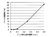
- bypass flow rate the relationship between the width of the upper portion of the fin portion, that is, the width of the bypass passage and the flow rate flowing through the bypass passage (hereinafter referred to as bypass flow rate) was examined by simulation.
- FIG. 12 shows the result.
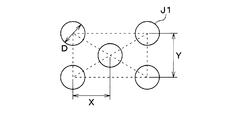
- a gap J3 between the straight fins J1 and the cooler J2 is changed using a simulation model in which a plurality of straight fins J1 are arranged in a staggered arrangement.
- the bypass flow rate was examined.
- the diameter of the straight fin J1 is D
- the height hc is 2 ⁇ D
- the pitch in the x direction between adjacent rows of the straight fins J1 is 2 ⁇ D
- the pitch in the y direction between the same rows was also 2 ⁇ D.
- coolant was assumed.
- the ratio of the bypass flow rate is as low as about 0 to 2%. At 15%. The ratio of the bypass flow rate increased as the gap J3 increased.
- the gap J3 exceeds 0.1 mm, the ratio of the bypass flow rate is significantly increased.
- the cylindrical portion in which a plurality of straight fins are formed is inserted into the cooling base, it is manufactured so that the cylindrical portion in which the plurality of straight fins are formed can be accurately inserted into the cooling base. It is necessary to set the height of the straight fins taking into account tolerances and warping of the fins. For this reason, the clearance gap between the front-end
- the tips of the fin portions 11c and 12c are in contact with the inner wall surface of the hollow plate-like portion 19c in the cooler 19 so that no gap is left between them. Therefore, it is possible to prevent a bypass passage from being formed between the tips of the fin portions 11c and 12c and the hollow plate-like portion 19c, and it is possible to suppress a decrease in heat dissipation efficiency.
- the tips of the fin portions 11c and 12c are tapered. For this reason, the fin parts 11c and 12c can be easily deformed in the height direction. Therefore, in the stacking direction of the semiconductor module 6 and the cooler 19, even if the dimension of the refrigerant passage 19b formed in the cooler 19 is smaller than the height of the fin portions 11c and 12c, due to the deformation of the fin portions 11c and 12c, The dimensional difference can be absorbed.
- the fin portion 11c is sized to the size of the refrigerant passage 19b formed in the cooler 19 in the stacking direction of the semiconductor module 6 and the cooler 19. , 12c may be brought close to each other. If the gap at this time is set to 0.1 mm or less, the ratio of the bypass flow rate can be reduced, so that a decrease in cooling efficiency can be suppressed.
- the dimension of the refrigerant passage 19b formed in the cooler 19 in the stacking direction of the semiconductor module 6 and the cooler 19 is the same as that of the fin portions 11c and 12c.
- the height is preferably smaller than the height.
- FIG. 14 is a diagram showing the evaluation results.
- SH-L in FIG. 14 uses an evaluation model in which the fin portions 11c and 12c are tapered as in this embodiment.
- FH-L in FIG. 14 uses an evaluation model in which the fin portions 11c and 12c have a constant diameter from the root to the tip as in the case of the straight fin.
- the amount of deformation was examined by changing the thickness at 2, 0.4 mm.
- the amount of deformation is large even with a low load.
- it becomes possible to obtain a desired amount of deformation with a low load by making the fin portions 11c, 12c into an elliptical arc shape with tapered tips. This is because the fin portions 11c and 12c are tapered elliptical arcs.
- the taper shape having a small cross-sectional area facilitates deformation
- the elliptical arc shape increases the amount of deformation in the z direction.
- the protruding amount L increases, the deformation region shifts to the tip portion, so that deformation in the z direction can be generated even with a lower load.
- the distortion of the fin portions 11c and 12c when the deformation is 0.1 mm which is the target value of the deformation, is calculated to be sufficiently smaller than 0.2%. It was confirmed. In the case of such a strain, the deformation of the fin portions 11c and 12c is a deformation in the elastic deformation region. Therefore, damage to the fin portions 11c and 12c can be suppressed.
- the digging direction and the refrigerant flow direction form an acute angle while the plurality of fin portions 11c and 12c are formed in an elliptical arc shape. Since it is set as such a structure, it becomes possible to improve the cooling performance by the several fin parts 11c and 12c, and it becomes possible to improve heat dissipation efficiency.
- heat transfer coefficient and pressure loss are indicators of cooling performance, depending on the shape of the fin part and how the refrigerant hits the fin part, even if the refrigerant path is determined Is different.
- a high heat transfer rate / pressure loss ratio can be said to be a cooler with high cooling performance.
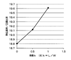
- thermal fluid analysis was performed on a model in which elliptical arc-shaped fins were arranged in a staggered arrangement.
- the protrusion amount L is based on the digging width W (corresponding to the width of the fin portion) corresponding to the digging depth.
- L 0, 0.5 ⁇ W, and 1.0 ⁇ W.
- the simulation was performed with the side positioned on the downstream side.
- k L / W
- the heat transfer rate / pressure loss ratio is high, and the digging direction is given a certain angle with respect to the x direction.
- the heat transfer coefficient / pressure loss ratio is further increased.
- the case where the fluid vector ⁇ is 135 to 225 ° means that the refrigerant flow direction is in the range of 0 to 45 ° with respect to the digging direction.
- the coolant flow direction is an acute angle in the range of greater than 0 ° and less than or equal to 45 ° with respect to the digging direction
- the heat transfer coefficient / pressure loss ratio increases when the coolant flow direction becomes an acute angle in the range of greater than 0 ° and less than 30 ° (the range of 150 ° to less than 180 ° in terms of fluid vector ⁇ ) with respect to the digging direction. Therefore, it can be said that these ranges have the highest cooling efficiency.
- the cooling performance by the plurality of fin portions 11c and 12c can be improved by making the digging direction and the coolant flow direction form an acute angle while making the plurality of fin portions 11c and 12c have an elliptical arc shape, and more heat dissipation efficiency. Can be improved.
- the recesses 11d and 12d are arranged on the downstream side of the refrigerant flow with respect to the fin portions 11c and 12c. For this reason, the influence which the recessed parts 11d and 12d have on a refrigerant
- coolant flow can be suppressed, and the improvement of cooling performance can be aimed at more.
- the fin portions 11c and 12c are used as simple straight pins, and there are no recesses 11d and 12d as shown by a broken line when there are recesses 11d and 12d as shown by a solid line.
- the cooling performance (heat transfer coefficient and pressure loss) was compared.
- the concave portions 11d and 12d are downstream of the refrigerant flow with respect to the fin portions 11c and 12c. It is arranged on the side, that is, on the back side of the flow velocity. Since the flow rate inevitably decreases in the vicinity of the back surfaces of the fin portions 11c and 12c when viewed from the flow rate, the influence can be reduced by bringing the recesses 11d and 12d to the back side where the flow rate decreases.
- the refrigerant flow in the z direction is also induced.
- the refrigerant flows in and the area in the recess is also used as a heat transfer surface. For this reason, it is effective for suppressing the influence by forming the recessed parts 11d and 12d.
- the convex surfaces of the fin portions 11c and 12c having an elliptical arc shape are positioned on the upstream side of the refrigerant flow, the refrigerant hits the mid-portion of the fin portions 11c and 12c and is in the z direction. Easy to induce flow to For this reason, the said effect can be acquired more.
- the fin portions 11c and 12c are formed in an elliptical arc shape while the fin portions 11c and 12c are formed by digging up. For this reason, the flow of the refrigerant
- the surface can be made flat before the fin portions 11c and 12c are dug up, and a semiconductor device capable of cooling the semiconductor module 6 with higher cooling efficiency can be obtained.
- the concave portions 11d and 12d are arranged on the downstream side of the refrigerant flow with respect to the fin portions 11c and 12c. Further, the fin portions 11c and 12c are formed in an elliptical arc shape, and the convex surface side is arranged on the upstream side of the refrigerant flow with respect to the concave surface side. The direction in which the fins 11c and 12c are dug up and the direction of the refrigerant flow form an acute angle. With these configurations, a semiconductor device capable of cooling the semiconductor module 6 with higher cooling efficiency can be obtained.
- the recesses 11d and 12d have the highest influence due to the positional relationship, and it is preferable to form the recesses 11d and 12d on the back side of the flow velocity with respect to the fin portions 11c and 12c.
- the fin portions 11c and 12c have an elliptical arc shape, comparing the case where the convex surface side is directed to the upstream side of the refrigerant flow and the case where the concave surface side is directed, the direction where the convex surface side is directed is 2 in the z direction. As a result, it was easy to induce the next flow, and the heat dissipation performance was improved, which was preferable.
- the digging direction of the fin portions 11c and 12c when the flow velocity vector ⁇ is set within a predetermined angle range so that the digging direction and the refrigerant flow direction form an acute angle (for example, 30 °), the digging direction and the refrigerant flow The heat dissipation performance was higher than when matching the direction.
- the fin portions 11c and 12c are elliptical arcs, either the case where the convex surface side is directed to the upstream side of the refrigerant flow or the case where the concave surface side is directed As for, the heat dissipation performance became higher.
- the fin portion after digging up so that the direction in which the convex surfaces of the fin portions 11c, 12c are directed forms an acute angle with respect to the refrigerant flow direction while the digging direction (x direction in the figure) of the fin portions 11c, 12c is directed to the refrigerant flow direction.
- 11c and 12c can be processed, processing is difficult.
- the substantially rectangular surface in which the through holes 19a on each of the refrigerant introduction side and the discharge side are provided with a plurality of fin portions 11c and 12c. And it is made to be located in the diagonal of the back surface heat sinks 11 and 12.
- the straight line connecting the centers of the through holes 19a and the x direction form an acute angle ⁇ greater than 0 ° and 45 ° or less while matching the direction in which the fins 11c and 12c are raised and the direction in which the convex surface is directed. I am doing so. Accordingly, the direction in which the fin portions 11c and 12c are dug up, that is, the direction in which the convex surface is directed and the direction of the refrigerant flow can be made to form an angle ⁇ .
- the fin portions 11c and 12c are formed in an elliptical arc shape by digging up the surfaces of the inner portions 11b and 12b, but the convex surface side of the fin portions 11c and 12c is the downstream side of the refrigerant flow, the concave surface The side is directed upstream of the refrigerant flow.
- the shape after digging is likely to be the shape as in this embodiment. For this reason, it is possible to easily process the fin portions 11c and 12c having the structure of the present embodiment.
- processing is difficult compared to the structure of this embodiment, such as performing shape processing of the fin portions 11c and 12c after digging up. Therefore, it is possible to simplify the manufacturing process when manufacturing the semiconductor device having the structure of the present embodiment.
- the fin portions 11c and 12c are digged up using the digging tool 100 having the cutting edge 100a.
- the cutting edge 100a is L-shaped bent in the vertical direction from the base 100b, and the tip is linear.
- the surface of the inner parts 11b and 12b is digged up so that the depth is constant from the middle position of the digging up while gradually raising the digging depth.
- the concave portions 11d and 12d are formed, the convex surface side faces away from the concave portions 11d and 12d, and the concave surface side faces the concave portions 11d and 12d. Can be formed.
- the surface of the fins 11c and 12c that has been dug is not a flat surface, but a curved surface that protrudes toward the recesses 11d and 12d.
- the recesses 11d and 12d are factors that affect the refrigerant flow. However, the smaller the volume in the recesses 11d and 12d, the less influence the refrigerant flow has. In addition, the shape of the fin portions 11c and 12c is advantageous when the pressure loss is taken into consideration.
- the cross-sectional shape of the fin portions 11c and 12c is a rectangular shape, and the cross-sectional shape of the concave portion is also a rectangular shape.
- the surface of the fin portions 11c and 12c that has been dug up is a curved surface, specifically an elliptical arc surface.
- the volumes in the recesses 11d and 12d are also the same as those in the first and second embodiments. Less than the structure. Therefore, it is possible to suppress the influence of the recesses 11d and 12d on the refrigerant flow, and further improve the cooling performance.
- Such a structure can be processed by changing the tip shape of the cutting edge 100a of the digging tool 100 as shown in FIG. That is, if the cutting edge 100a is semi-elliptical arc, the cross-sectional shape of the digging surface of the fin portions 11c and 12c formed by digging can be an elliptical arc-shaped curved surface.
- the cross-sectional shape of the fin parts 11c and 12c was made into the elliptical arc-shaped curved surface as an example which made the tapering shape the surface side which digged up among the fin parts 11c and 12c.
- Other tapered shapes for example, as shown in FIG. 28, the surface of the fin portions 11c and 12c that have been dug up may be a V-shaped surface. Even if it does in this way, the effect similar to 3rd Embodiment can be acquired.
- Such a structure can be processed by making the tip shape of the cutting edge 100a of the digging tool 100 V-shaped as shown in FIG.
- two semiconductor modules 6 are provided, and two semiconductor modules 6 are arranged between three coolers 19. Specifically, one semiconductor module 6 is disposed on both sides of one cooler 19, and one cooler 19 is disposed on both sides so as to sandwich two semiconductor modules 6 and one cooler 19. The structure is arranged.
- the cooler 19 sandwiched between the two semiconductor modules 6 has openings 19e on both sides of the front and back surfaces.
- the inner portion 11b and the fin portion 11c of the upper radiator plate 11 of one semiconductor module 6 are inserted into one opening portion 19e, and the lower radiator plate 12 of the other semiconductor module 6 is inserted into the other opening portion 19e.
- the inner part 12b and the fin part 12c are inserted.
- the dimension hc of the flow passage 19b formed in the cooler 19 in the height direction of the fin portions 11c and 12c is made smaller than the sum of the heights 2 ⁇ dc of both the fin portions 11c and 12c. Yes. By doing in this way, it can prevent that a clearance gap is formed between both the front-end
- a semiconductor device in which a plurality of semiconductor modules 6 are stacked in this way is applied to an inverter unit as shown in FIG. 33, for example.
- the inverter unit shown in FIG. 33 has a substantially rectangular parallelepiped shape, and on one surface side, a pipe member 200 connected to the passage component 19b in the stacking direction of the semiconductor module 6 and the cooler 19 is provided.
- a nut portion 201 is provided at the tip of the pipe member 200, and the nut portion 201 is connected to another pipe member (not shown) to introduce and discharge the refrigerant.
- one end side of the multilayer wiring bus bar 13 protrudes from one surface having one direction orthogonal to the stacking direction of the semiconductor modules 6 and the cooler 19 as a normal direction, and the other end side of the multilayer wiring bus bar 13 extends from the surface opposite to the one surface. It sticks out.
- a positive electrode terminal 202a and a negative electrode terminal 202b are connected to the positive electrode and negative electrode terminals 13a and 13b arranged on one end side of the multilayer wiring bus bar 13, and a positive electrode and a negative electrode of a power source (not shown) are connected to each of these terminals 202a and 202b. Supply is made.
- U, V and W terminals 202c to 202e are connected to U to W terminals 13c to 13e arranged on the other end side of the multilayer wiring bus bar 13. These terminals 202c to 202e are connected to U to W terminals of a motor (not shown) driven by an inverter unit to supply current corresponding to each phase.
- the two semiconductor modules 6 can be driven in parallel or different motors.
- the two motors can be driven by connecting to the U to W terminals. In that case, if the positive and negative terminals 13a, 13b of the two semiconductor modules 6 are connected to different power sources, the two motors can be driven by different voltages.
- the inverter unit has an outer frame portion configured by columnar stays 204 arranged at four corners and a support member 205 that extends in the stacking direction of the semiconductor modules 6 and connects the two stays 204. Surrounded.
- a printed circuit board 206 provided with a control circuit is fixed to both ends of each stay 204 in the outer frame portion by screws or the like.
- the control terminal 14 is inserted into a through hole formed in the printed board 206 and soldered, whereby the control terminal 14 and the control circuit are electrically connected.
- the capacitor module 207 which comprises the smoothing capacitor 4 is being fixed to the surface of the cooler 19 in the one surface side in which the pipe member 200 was provided.
- the capacitor module 207 is a ceramic capacitor made of, for example, barium titanate having a high dielectric constant, and is a plate-like member.
- the capacitor module 207 may be constituted by a film capacitor such as PP material, but by using a small and large-capacity ceramic capacitor, a small space where the cooler 19 is disposed can be effectively used.
- the capacitor module 207 can be mounted. As a result, the inverter unit can be miniaturized.
- FIG. 1 a structure having a plurality of semiconductor modules 6 can be provided.
- an inverter unit can also be comprised by the structure provided with several such semiconductor modules 6.
- the tip is tapered, and the digging direction and the direction of the refrigerant flow form an acute angle.
- the semiconductor switching elements 51a to 56a have been described as examples of the heat generating elements.
- any semiconductor device in which a semiconductor element serving as a heat generating element is formed and the semiconductor element is cooled by the cooler 19 may be used.
- the present disclosure can be applied to the configuration.
- the fin portions 11c and 12c have an elliptical arc shape
- the elliptical arc shape is a concept including an arc shape.
- the fins 11c and 12c have the same thickness from the base part to the middle abdomen, and the taper gradually decreases in thickness from the middle part to the tip part, but the whole area extends from the root part to the tip part. It may be a tapered shape in which the thickness gradually decreases over time.
- the mode in which the positive electrode side and the positive electrode terminal 13a of the DC power source 2 serving as the external power source are directly connected to each other and the negative electrode side and the negative electrode terminal 13b are directly connected is described.
- the negative terminal 13b is a terminal connected to a low potential point. For this reason, an element such as a resistor may be provided between the positive electrode terminal 13a and the external power supply or between the negative electrode terminal 13b and the ground potential point.
Landscapes
- Engineering & Computer Science (AREA)
- Physics & Mathematics (AREA)
- Power Engineering (AREA)
- General Physics & Mathematics (AREA)
- Computer Hardware Design (AREA)
- Microelectronics & Electronic Packaging (AREA)
- Condensed Matter Physics & Semiconductors (AREA)
- Manufacturing & Machinery (AREA)
- Thermal Sciences (AREA)
- Mechanical Engineering (AREA)
- General Engineering & Computer Science (AREA)
- Cooling Or The Like Of Semiconductors Or Solid State Devices (AREA)
- Cooling Or The Like Of Electrical Apparatus (AREA)
Abstract
半導体装置は、半導体素子(51a~56a)と、前記半導体素子を覆う樹脂モールド部(18)と、前記樹脂モールド部に封止されると共に、該樹脂モールド部の一面から露出させられ、前記半導体素子の発した熱の放熱を行う放熱板(11、12)と、を有する半導体モジュール(6)と、前記半導体モジュールにおける前記放熱板が露出させられている一面に配置され、冷媒通路(19b)を構成し、該冷媒通路内に冷媒が流されることで前記放熱板からの放熱を促進させる冷却器(19)と、を備える。前記放熱板には、該放熱板の表面を掘り起こして形成されたフィン部(11c、12c)が備えられる。該フィン部は先細り形状とされると共に根元部から先端部に至るまで湾曲した楕円弧状とされている。
Description
本出願は、2015年6月12日に出願された日本特許出願番号2015-119459号に基づくもので、ここにその記載内容を援用する。
本開示は、発熱素子が備えられた半導体モジュールを冷却器にて冷却する構造の半導体装置に関するものである。
電動システムの高出力化に伴って、半導体モジュールに備えられるパワー素子の発熱量が増加している。熱抵抗Rthは、発熱素子となるパワー素子の発熱温度をΔTj、発熱量をPとすると、次式で表される。
(数1) Rth(℃/W)=ΔTj÷P
これは、熱抵抗の低い半導体モジュールでは、同じ発熱量であってもΔTjが高くなることを示している。しかしながら、熱抵抗が高いと、温度上限から高電流を流せない。このため、所望の出力(例えば100Arms)を流すためには素子を並列接続したり、素子サイズを増加させることが必要となる。これにより、パワー素子を構成するチップ面積の増大ひいてはコスト増大を招く。すなわち、熱抵抗が高いほどコストが増大するという関係を有していることから、放熱効率を高めることで素子発熱温度を低下させ、素子サイズの縮小を図ることが重要となる。
これは、熱抵抗の低い半導体モジュールでは、同じ発熱量であってもΔTjが高くなることを示している。しかしながら、熱抵抗が高いと、温度上限から高電流を流せない。このため、所望の出力(例えば100Arms)を流すためには素子を並列接続したり、素子サイズを増加させることが必要となる。これにより、パワー素子を構成するチップ面積の増大ひいてはコスト増大を招く。すなわち、熱抵抗が高いほどコストが増大するという関係を有していることから、放熱効率を高めることで素子発熱温度を低下させ、素子サイズの縮小を図ることが重要となる。
このため、半導体モジュールを有する半導体装置では、半導体モジュールの放熱効率を高めるために、半導体モジュールにフィン部が形成された放熱板を備えると共に、フィン部を覆うように冷却器を配置している。冷却器の内部空間に冷媒を流動させることで半導体モジュールの放熱を促進させ、半導体モジュールに放熱板を備えることでさらに放熱効率が高められる。
例えば、放熱板として、特許文献1に示すような金属板を堀り起こしてフィン部を構成するものがある。フィン部は、直線状もしくは破線状の刃部を有する掘り起こし工具によって掘り起こされることで構成され、直線状もしくは複数が等間隔に破線状に配置された構成とされている。
また、冷媒通路を構成した冷却ベースの開口部から円柱形状のストレートフィンが複数形成された放熱板を有する筒部を挿入し、筒部の挿入方向後端に備えられたフランジ部にて冷却ベースに筒部を固定する構造のものもある。フランジ部と冷却ベースとの間にはシール部材が設けられ、冷却ベースの開口部はフランジ部およびシール部材によって密閉される。そして、冷却ベース内に形成された冷媒通路に冷媒を流すと、ストレートフィンに衝突するようにして冷媒が流れる。これにより、高い放熱効率が得られるようにしている。
しかしながら、特許文献1のように直線状もしくは破線状の刃部を有する掘り起こし工具によってフィン部を掘り起こす形態では、表面積を大きく取って伝熱面を拡げていることから、フィン部を掘り起こす方向に対する垂直方向が冷媒流れ方向となる。すなわち、直線状もしくは破線状に形成されたフィン部が複数列並列的に配置され、複数列のフィン部の間を通過するように冷媒が流れることとなる。このように冷媒流れが一様になることから、冷却効率を高めることが難しい。これは、空冷方式のように冷媒として空気などの気相冷媒が用いられる場合であっても、水冷方式のように冷媒として水などの液相冷媒が用いられる場合であっても同様のことが言える。
また、ストレートフィンが複数形成された放熱板を有する筒部を冷却ベースに挿入する形態では、筒部を冷却ベースの冷媒通路内に挿入できるように、ストレートフィンの先端と冷媒通路の内壁面との間に隙間を設ける必要がある。この隙間をバイパス通路として冷媒がフィン部を通じることなく抜けてしまうため、熱伝達率が下がり、放熱効率を低下させてしまう。また、ストレートフィンを成形などによって形成していて、初めから放熱板の表面が平坦面ではないことから、素子部の接合状態を超音波映像装置(SAT)などによって検査することが難しい。
本開示は、掘り起こしによって構成されるフィン部とすることで、掘り起こし前に表面を平坦面とすることが可能で、かつ、より高い冷却効率で半導体モジュールを冷却することが可能な半導体装置を提供することを目的とする。
本開示の態様において、半導体装置は、発熱素子となる半導体素子と、前記半導体素子を覆う板状の樹脂モールド部と、前記樹脂モールド部に封止されると共に、該樹脂モールド部の一面から露出させられ、前記半導体素子と絶縁されつつ、前記半導体素子の発した熱の放熱を行う放熱板と、を有する少なくとも一つの半導体モジュールと、前記半導体モジュールにおける前記放熱板が露出させられている一面に配置され、冷媒通路を構成し、該冷媒通路内に冷媒が流されることで前記放熱板からの放熱を促進させる冷却器と、を備える。前記放熱板には、該放熱板の表面を掘り起こして形成されたフィン部が備えられる。該フィン部は先細り形状とされると共に根元部から先端部に至るまで湾曲した楕円弧状とされている。
上記の半導体装置において、掘り起こしによってフィン部を形成すると共に、フィン部を楕円弧状としている。そして、フィン部が楕円弧状とされていることから、フィン部の高さ方向への冷媒の流れを発生させることができる。これらの構成により、フィン部を掘り起こす前には表面を平坦面にできるし、より高い冷却効率で半導体モジュールを冷却することが可能な半導体装置にできる。
本開示についての上記目的およびその他の目的、特徴や利点は、添付の図面を参照しながら下記の詳細な記述により、より明確になる。その図面は、
図1は、本開示の第1実施形態にかかる半導体装置に備えられる半導体モジュールが構成する三相インバータ回路の回路図であり、
図2は、半導体モジュールの斜視図であり、
図3は、半導体モジュールの両面を冷却機器によって挟む様子を示した斜視図であり、
図4は、半導体モジュールの構成部品の分解斜視図であり、
図5は、半導体モジュールの上面レイアウト図であり、
図6は、多層配線バスバーの斜視図であり、
図7は、半導体装置の断面図であり、
図8は、半導体装置の分解図であり、
図9は、半導体モジュールの上面図であり、
図10は、フィン部近傍の断面図であり、
図11は、フィン部上面図であり、
図12は、フィン部の上部の隙間とバイパス流量割合の関係をシミュレーションした結果を示す図であり、
図13(a)は、図12のシミュレーションに用いたモデルの上面レイアウト図であり、
図13(b)は、図12のシミュレーションに用いたモデルの断面図であり、
図14は、印加荷重に対する変形量の関係を示した図であり、
図15(a)は、図14のシミュレーションに用いたモデルの断面図であり、
図15(b)は、図14のシミュレーションに用いたモデルの断面図であり、
図16は、楕円弧状のフィンのモデルの断面図であり、
図17は、係数kと熱伝達率/圧損比率との関係を示した図であり、
図18は、流体ベクトルと熱伝達率/圧損比率との関係を示した図であり、
図19は、規格化圧力損失と規格化熱伝達率との関係を示した図であり、
図20は、冷却性能の比較に用いたモデルの断面図であり、
図21は、凹部内における流速コンター図であり、
図22は、ストレートフィンを基準とした場合における各種構造ごとの冷却効率を調べた結果を示す図であり、
図23は、冷媒流れの方向とフィン部の掘り起こし方向との関係を示した図であり、
図24は、本開示の第2実施形態にかかるフィン部の断面図であり、
図25(a)は、掘り起こし工具の側面図であり、
図25(b)は、掘り起こし工具の正面図であり、
図25(c)は、掘り起こし工具によって掘り起こしたフィン部の断面図であり、
図26は、本開示の第3実施形態にかかるフィン部の上面図であり、
図27は、図26に示すフィン部の形成に用いる掘り起こし工具の正面図であり、
図28は、第3実施形態の変形例にかかるフィン部の上面図であり、
図29は、図28に示すフィン部の形成に用いる掘り起こし工具の正面図であり、
図30は、本開示の第4実施形態にかかる半導体装置の斜視図であり、
図31は、図30に示す半導体装置の分解図であり、
図32は、2枚の半導体モジュールそれぞれのフィン部た断面図であり、
図33は、複数枚の半導体モジュールを積層した半導体装置が適用されるインバータユニットの斜視図である。
以下、本開示の実施形態について図に基づいて説明する。なお、以下の各実施形態相互において、互いに同一もしくは均等である部分には、同一符号を付して説明を行う。
(第1実施形態)
本開示の第1実施形態について説明する。本実施形態では、本開示の一実施形態にかかる半導体モジュールを有する半導体装置の適用例として、例えば三相交流モータなどの駆動を行う三相インバータ回路が備えられた半導体モジュールを有する半導体装置を例に挙げて説明する。
本開示の第1実施形態について説明する。本実施形態では、本開示の一実施形態にかかる半導体モジュールを有する半導体装置の適用例として、例えば三相交流モータなどの駆動を行う三相インバータ回路が備えられた半導体モジュールを有する半導体装置を例に挙げて説明する。
まず、図1を参照して、半導体モジュールに備えられる三相インバータ回路1の構成について説明する。図1に示すように、三相インバータ回路1は、直流電源(外部電源)2に基づいて三相交流モータなどの負荷3を駆動するためのものである。三相インバータ回路1には平滑コンデンサ4が並列接続されており、スイッチング時のリプルの低減やノイズの影響を抑制して一定な電源電圧が形成できるようにしてある。
三相インバータ回路1は、直列接続した上下アーム51~56が三相分並列接続された構成とされ、上アーム51、53、55と下アーム52、54、56との各中間電位を負荷3となる三相交流モータのU相、V相、W相の各相に順番に入れ替えながら印加する。具体的には、上下アーム51~56は、それぞれ、発熱素子となるIGBTやMOSFETなどの半導体スイッチング素子51a~56aおよびFWDなどの還流を目的とした整流素子(片側導通素子)51b~56bを備えた構成とされる。そして、各相の上下アーム51~56の半導体スイッチング素子51a~56aがオンオフ制御されることで、三相交流モータに対して周期の異なる三相の交流電流を供給する。これにより、三相交流モータの駆動を可能としている。
本実施形態では、三相インバータ回路1に備えられる6つの上下アーム51~56それぞれを構成する半導体スイッチング素子51a~51fおよび整流素子51b~56bが形成された半導体チップをモジュール化して一体化している。つまり、6つのアームを一体化した6in1構造の半導体モジュールとして三相インバータ回路1を構成している。
続いて、上記のような回路構成の三相インバータ回路1が備えられた半導体モジュールを有する半導体装置の詳細構造について、図2~図8を参照して説明する。
図2に示す半導体モジュール6は、図4に示すように、半導体チップ10、上側および下側放熱板11、12、各種端子や配線を一体化した多層配線バスバー13、制御端子14、素子中継電極15およびプレート16、17などを備えた構成とされている。これらのうちの半導体チップ10、制御端子14、素子中継電極15およびプレート16、17などを1アーム分の構成部品ブロックとして、6組の構成部品ブロックが備えられている。そして、6組の構成部品ブロックを多層配線バスバー13と共に上側および下側放熱板11、12で挟み込み、図2に示すように樹脂モールド部18で覆っている。このようにして、半導体モジュール6は、図2に示すように所定の厚みを有する板状部材として構成されている。このような半導体モジュール6は、図3に示すように厚み方向の両側を冷却器19によって挟み込まれることで、放熱を行いながら負荷3の駆動を行うものとして使用される。なお、各冷却器19の相対する二角には貫通孔19aが設けられていると共に、各貫通孔10aそれぞれを繋いで冷媒通路を構成する通路構成部19dが備えられる。これにより、冷却器19の冷却が行われることで、効率的な冷却を可能にしながら半導体モジュール6が使用される。
以下、半導体モジュール6を有する半導体装置の詳細構造について説明するが、樹脂モールド部18にて覆った6アーム分の構成部品ブロックそれぞれの詳細構造は、若干異なっているものの基本構造が同様である。まずは、この樹脂モールド部18にて覆っている構成部品ブロックの基本構造を構成している各部品について説明する。
図4に示す半導体チップ10は、6個のチップ10a~10fによって構成されている。各チップ10a~10fは、表面および裏面を有し、それぞれに上アーム51、53、55もしくは下アーム52、54、56を構成する半導体スイッチング素子51a~56aや整流素子51b~56bなどが形成されている。例えば、半導体チップ10は、Si、SiC、GaNなどの半導体基板を母材基板として用いて形成されている。本実施形態では、半導体チップ10に形成される半導体スイッチング素子51a~56aや整流素子51b~56bを基板垂直方向に電流を流す縦型素子としており、半導体チップ10の表面側と裏面側に各種電極(パッド)が形成され、この電極を介して電気的接続が行われている。本実施形態の場合、各半導体チップ10の裏面側は、はんだやAg焼結材のような高熱伝導材で構成された接合材20を介して下側プレート17の表面側に電気的および物理的に接続されている。そして、下側プレート17の裏面側がはんだやAg焼結材のような高熱伝導材で構成された接合材21を介して下側放熱板12に接合されている。
また、半導体チップ10の表面側は、Cu、Al、Fe等を母材として構成された素子中継電極15に対して、はんだやAg焼結材のような高熱伝導材で構成された接合材22を介して接続されている。さらに、素子中継電極15がはんだやAg焼結材のような高熱伝導材で構成された接合材23を介して上側プレート16の裏面側に電気的および物理的に接続されている。そして、上側プレート16の表面側がはんだやAg焼結材のような高熱伝導材で構成された接合材24を介して上側放熱板11に接合されている。
このような構造により、各半導体チップ10が上側および下側放熱板11、12に対して挟み込まれた構造とされている。
なお、本実施形態では、半導体チップ10は、各アーム51~56を構成する半導体スイッチング素子51a~56aや整流素子51b~56bなどの素子が1チップ内に共に形成されたものとされている。しかしながら、これは単なる一例を示したものであり、各アーム51~56を構成する半導体スイッチング素子51a~56aや整流素子51b~56bなどの素子が別々のチップに形成されていても良い。
上側および下側放熱板11、12は、ヒートシンクに相当するもので、例えばCu、Al、Fe等を主成分とした高熱伝導部材で構成され、一面側が半導体チップ10に向けられ、他面側が図2に示されるように樹脂モールド部18から露出させられている。上側および下側放熱板11、12は、段付形状とされており、外縁部11a、12a(図7参照)に対してそれよりも内側となる内側部11b、12b(図7参照)の方が所定量突出させられている。具体的には、外縁部11a、12aは、その周囲における樹脂モールド部18の一面と同一平面とされており、内側部11b、12bが樹脂モールド部18から所定距離突き出した構成とされている。そして、内側部11b、12bに、内側部11b、12bの表層部を掘り起こし工具によって掘り起こした複数のフィン部11c、12cが形成されている。この複数のフィン部11c、12cの詳細構造については後述する。なお、図7では、樹脂モールド部18内に備えられる各部品については図示しないを省略してある。
また、上側および下側放熱板11、12は、上側および下側プレート16、17が部分的に絶縁材料で構成されることで、半導体チップ10とは絶縁された状態となっている。ただし、上側および下側プレート16、17や素子中継電極15等が高熱伝導材料で構成されていることから、上側および下側放熱板11、12には、半導体チップ10からの熱が高い熱伝導で伝えられる。そして、上側放熱板11のうちの表面側および下側放熱板12のうちの裏面側、つまりフィン部11c、12cが形成された面から放熱が行えるようになっている。
多層配線バスバー13は、本実施形態の半導体モジュール6のうちの各種配線や各種端子を構成する部分である。本実施形態では、多層配線バスバー13は、板状棒状部材で構成され、各相の上アーム51、53、55を構成する半導体チップ10と下アーム52、54、56を構成する半導体チップ10の間を通過するように配置されている。例えば、多層配線バスバー13には、上アーム51、53、55と直流電源2の+端子とを接続する正極側配線、下アーム52、54、56と直流電源2の-端子とを接続する負極側配線、各アーム51~56と負荷3とを接続する出力配線が備えられている。また、多層配線バスバー13には、各配線と直流電源2や負荷3との接続を行うための各種接続端子13a~13eが備えられている。
具体的には、図6に示すように、多層配線バスバー13は、一方向を長手方向とした板状棒状部材によって構成されており、図2に示すように一端側と他端側がそれぞれ略四角形状とされた樹脂モールド部18の相対する二辺それぞれから露出させられている。
図6に示すように、多層配線バスバー13の一端側には、上アーム51、53、55と直流電源2の+端子とを接続する正極端子13aおよび下アーム52、54、56と直流電源2の-端子とを接続する負極端子13bが形成されている。また、多層配線バスバー13の他端側には、各U相、V相、W相の各相における上下アーム51~56の中間電位点と負荷3とを接続する出力端子に相当するU端子13c、V端子13d、W端子13eが備えられている。これら正極端子13a、負極端子13b、U端子13c、V端子13d、W端子13eは、図2に示すように樹脂モールド部18から露出させられている。このような構成により、正極端子13aおよび負極端子13bを介して半導体モジュール6と直流電源2や平滑コンデンサ4との電気的接続が行われている。また、U端子13cやV端子13dおよびW端子13eを介して負荷3となる三相交流モータのU相やV相およびW相との電気的接続が行われている。
このような多層配線バスバー13は、パターニングされた導体層と絶縁層とを積層した多層配線構造によって構成されており、図1に示した三相インバータ回路1の各部を電気的に接続する回路配線を構成している。なお、多層配線バスバー13に備えられた各パッド136a~136c、139a~139cは、半導体チップ10a~10fの所定部位に電気的に接続される。図示しないが、多層配線バスバー13のうち各パッド136a~136c、139a~139cが配置された面と反対側の面にも、半導体チップ10a~10fの所定部位に電気的に接続される複数のパッドが備えられている。そして、多層配線バスバー13に備えられる内部配線と各パッド136a~136c、139a~139cが電気的に接続され、内部配線と各端子13a~13eとが電気的に接続されることで、三相インバータ回路1の配線構造が構成されている。内部配線は、絶縁膜130によって被覆されており、絶縁膜130から露出するようにして各パッド136a~136c、139a~139cや各端子13a~13eが設けられている。
制御端子14は、半導体スイッチング素子51a~56aのゲート配線などの各種信号線を構成する信号線端子となるものある。例えば、制御端子14は、半導体チップ10の表面側に形成された半導体スイッチング素子51a~56aのゲートに接続される電極にAu等で構成されるボンディングワイヤ25(図4参照)を介して電気的に接続されている。制御端子14における半導体チップ10とは反対側の端部は、図2に示すように樹脂モールド部18から露出させられており、この露出部分を通じて外部との接続が行えるように構成されている。なお、図4中では、制御端子14がリードフレーム状態で一体化されたものとして記載してあり、下側放熱板12とも一体化された状態とされているが、最終製品とされる際に分断され、各信号線が独立した状態となる。
素子中継電極15は、半導体チップ10側の一面において半導体チップ10の表面の電極との電気的な接続を図りつつ、上側プレート16と電気的に接続される部材である。素子中継電極15は、半導体チップ10と上側プレート16との間をボンディングワイヤ25が配置される分の間隔空けるために備えられている。素子中継電極15は、例えばCu等を主成分とした高熱伝導部材で構成されている。
上側プレート16は、半導体チップ10側の一面において素子中継電極15を介して半導体チップ10の表面の電極との電気的な接続を図りつつ、半導体チップ10と上側放熱板11とを絶縁する役割を果たす。同様に、下側プレート17は、半導体チップ10側の一面において半導体チップ10の裏面の電極との電気的な接続を図りつつ、半導体チップ10と下側放熱板12とを絶縁する役割を果たす。
上側および下側プレート16、17のうちの半導体チップ10側の一面は電気的な接続に加えて熱伝導性が高められるように、Cu、Al等を母材とする高熱伝導部材によって構成されている。また、上側および下側プレート16、17のうち、半導体チップ10側の一面よりも半導体チップ10と反対側に位置する層は、絶縁を図りつつ熱伝導性が高められるように、例えば無機もしくは有機系絶縁材料で構成されている。例えば、Si3N4、AlN、Al2O3等のセラミックス絶縁体の両面にCuを母材とする導体板を貼り合せたものによって上側および下側プレート16、17を構成できる。また、絶縁シートを貼り付けたCuプレートと絶縁接着機能を有する接着剤シートをCu等の導体部材で構成されるダイボンドプレートと貼り合せたものによって上側および下側プレート16、17を構成することもできる。
このような構成とされることで、上側プレート16は、半導体スイッチング素子51a~56aの表面電極(例えばMOSFETのソースやIGBTのエミッタ)および整流素子51b~56bの第1電極(例えばFWDなどのアノード)と接続される。また、上側プレート16は多層配線バスバー13に備えられる各パッド136a~136c、139a~139cとも電気的に接続されている。同様に、下側プレート17については、半導体スイッチング素子51a~56aの裏面電極(例えばMOSFETのドレインやIGBTのコレクタ)および整流素子51b~56bの第2電極(例えばFWDなどのカソード)と接続される。また、下側プレート17も多層配線バスバー13の裏面側に備えられる各パッド(図示せず)とも電気的に接続されている。このため、上側および下側プレート16、17は、各アーム51~56に対しての正極側配線や負極側配線および出力配線の一部を構成している。
また、上記したように、上側放熱板11のうちの表面側および下側放熱板12のうちの裏面側、つまり半導体チップ10が配置される面と反対側の面は共に、樹脂モールド部18から露出させられており、この露出部分において、放熱が行えるようになっている。この放熱面側には、図3に示すように冷却器19が配置される。冷却器19は、図7に示すように内部に形成される空洞部によって流動通路19bが構成されており、この流動通路19b内を冷媒が流動させられるようになっている。このため、上側および下側放熱板11、12の放熱面が冷媒に接することになるが。しかしながら、上側および下側プレート16、17によって半導体チップ10と上側および下側放熱板11、12との間の絶縁が図られていることから、上側および下側放熱板11、12を通じて外部に電流リークが生じることを防止できる。
樹脂モールド部18は、上記した各構成部品を成形型内に配置したのち、成形型内に樹脂を封入することで構成された封止樹脂であり、例えば四角形板状で構成されている。樹脂モールド部18は、絶縁性で、かつ、上側および下側放熱板11、12などの導体部より低い線膨張係数およびヤング率の樹脂で構成される。例えば、主にエポキシ、シリコーン等の有機樹脂によって樹脂モールド部18を構成することができる。樹脂モールド部18からは、四角形板状を構成する各辺から制御端子14の先端および多層配線バスバー13の両端が露出させられており、外部との電気的接続が行えるようになっている。具体的には、四角形板状とされる樹脂モールド部18の相対する2辺より、つまり樹脂モールド部18を挟んだ反対方向に、上アーム51、53、55の制御端子14と下アーム52、54、56の制御端子14が露出させられている。また、四角形板状とされる樹脂モールド部18の異なる相対する2辺より、つまり樹脂モールド部18を挟んだ反対方向に、多層配線バスバー13の両端がそれぞれ露出させられている。また、四角形板状の表裏面それぞれから上側放熱板11と下側放熱板12が露出させられ、良好に放熱が行える構造とされている。
具体的には、制御端子14が一体化されたリードフレーム状態の下側放熱板12の表面側に、上述した各部を搭載する。そして、ボンディングワイヤ25にて半導体チップ10と制御端子14との電気的な接続を終えたのち、その上に上側放熱板11などを搭載する。この状態でこれらを成形型に設置し、成形型内に樹脂を注入してモールド化することで樹脂モールド部18が構成される。この樹脂モールド部18により、上側および下側放熱板11、12の表面に加えて、制御端子14および多層配線バスバー13の露出箇所以外が覆われることで、半導体チップ10などが保護される。
冷却器19は、内部に冷媒通路19bを構成し、冷媒が流動させられることで半導体モジュール6の放熱を促進させるものである。冷却器19は、半導体モジュール6における上側および下側放熱板11、12が配置された両放熱面に配置され、冷却器19によって半導体モジュール6を挟み込むように冷却器19および半導体モジュール6が積層されている。そして、図8に示すように、2つの冷却器19によって半導体モジュール6を挟みつつ、冷却器19および半導体モジュール6をボルト28で締結することで、これらが一体化されている。
具体的には、冷却器19は、図3に示すように、半導体モジュール6と反対側から見た形状が略長方形状とされた中空板状部19cと貫通孔19aが形成された通路構成部19dとを有した構成とされる。中空板状部19c内に構成される中空部を冷媒通路10bとして、一方の貫通孔19aより導入される冷媒が冷媒通路19bを通過したのち、他方の貫通孔19aより排出される。
図7に示すように、中空板状部19cのうち半導体モジュール6側の一面には、冷媒通路19bに繋がる開口部19eが形成されている。この開口部19e内に内側部11b、12bおよびフィン部11c、12cが配置される。内側部11b、12bの外縁形状と開口部19eの形状は一致させられており、内側部11b、12bが開口部19eに嵌め込まれるようにして、冷却器19が半導体モジュール6に組み付けられる。
中空板状部19cのうち半導体モジュール6側の一面は所定の厚みを有した構造とされるが、その厚みが内側部11b、12bの外縁部11a、12aからの突き出し量と一致させられている。
また、図8に示すように、冷却器19と半導体モジュール6との間に、開口部19eを囲むシール部材26が配置されている。このため、冷却器19と半導体モジュール6との間がシール部材26によってシールされ、冷媒漏れが防止されている。
なお、後述するように、半導体モジュール6と冷却器19の積層方向において、冷却器19に形成された冷媒通路19bの寸法がフィン部11c、12cの高さより小さくされている。また、フィン部11c、12cの先端が先細りとされていて変形し易くなっている。このため、フィン部11c、12cは、半導体モジュール6と冷却器19とを組み付けたときに、冷媒通路19bを構成する冷却器19の内壁面にフィン部11c、12cの先端が当接すると共に、当接したときにフィン部11c、12cの先端が変形する。これにより、冷却器19と半導体モジュール6との間において、シール部26が隙間無く配置され、的確にシール機能を発揮できるようになっている。
通路構成部19dは、図3に示すように長方体形状とされていて、その中心位置に貫通孔19aが形成されている。隣り合う冷却器19の通路構成部19dは、貫通孔19aを囲むシール部材27を介して互いに密着させられており、互いの貫通孔19aが繋げられている。貫通孔19aは、冷媒通路19bと連通させられている。このため、互いに密着させられた一方の通路構成部19dの貫通孔19aより導入される冷媒は、冷媒通路10bを通過して、互いに密着させられた他方の通路構成部19dの貫通孔19aより排出される。
なお、上記したように、半導体モジュール6と冷却器19の積層方向において、冷却器19に形成された冷媒通路19bの寸法がフィン部11c、12cの高さより小さくされているが、フィン部11c、12cの先端位置が変形し易くなっている。このため、隣り合う通路構成部19d同士の間において、シール部26が隙間無く配置され、的確にシール機能を発揮できるようになっている。
また、貫通孔19aおよび通路構成部19dは、冷却器19を半導体モジュール6と反対側から見たときの略長方形状における対角の関係に位置する2つの角部に配置されている。具体的には、多層配線バスバー13における正極および負極端子13a、13bが配置された側の端部と、U~W端子13c~13eが配置された側の端部が略長方形状とされる冷却器19のもう一方の対角の関係に位置する2つの角部より突き出すように配置されている。これら各端子13a~13eとずらされた位置に貫通孔19aが配置されている。このため、冷却器19のうち貫通孔19aおよび通路構成部19dによって隠れることなく、各端子13a~13eと外部配線との電気的接続が行えるようになっている。
以上のような構造により、本実施形態にかかる半導体モジュール6を有する半導体装置が構成されている。続いて、放熱板11、12に形成された複数のフィン部11c、12cの詳細構造について、図2、図7および図9~図11を参照して説明する。なお、ここでは複数のフィン部11cについて主に説明するが、複数のフィン部12cも複数のフィン部11cと同様の構成とされている。
図2および図9に示すように、内側部11bは、多層配線バスバー13の長手方向と同方向を長辺、それに対する垂直方向を短辺とする長方形状とされている。図2に示すように、この内側部11bの長辺方向をx方向、短辺方向をy方向、内側部11bの法線方向をz方向として、複数のフィン部11cは、x方向およびy方向において所定のレイアウトで配列されている。そして、内側部11bの表面を掘り起こし工具でz軸方向に掘り起こすことで、複数のフィン部11cの1つ1つが構成されている。
本実施形態の場合、複数のフィン部11cは、y方向において等間隔に複数本が並べられた列がx方向において等間隔に複数列並べられている。そして、隣り合う列のフィン部11cのy方向の形成位置がずらされており、y方向において、各列の各フィン部11cが隣の列の隣り合うフィン部11cの中間位置に配置されたレイアウト、つまり千鳥配列のレイアウトで複数のフィン部11cが配列されている。
一方、図9に示すように、冷却器19における冷媒流れ方向は、冷媒が導入される側の貫通孔19aから冷媒が排出される側の貫通孔19aに向かう方向となり、図中矢印A1で示した方向となる。したがって、千鳥配列とされた複数のフィン部11cは、冷媒流れ方向に沿った配列となる。なお、ここでいう複数のフィン部11cが冷媒流れ方向に沿って配列されているとは、複数のフィン部11cが冷媒流れ方向と平行になっていなくても良く、その配列方向と冷媒流れ方向とに角度が付いていても良い。ただし、両貫通孔19aの中心位置を通る直線(図中矢印A1)に対して、複数のフィン部11cが平行に配列されるようにしてあると、冷媒流れを阻害せず、圧力損失を少なくできることから好ましい。
また、複数のフィン部11cは、それぞれy方向に沿って内側部11bの表面を掘り起こすことによって形成されている。このため、複数のフィン部11cの掘り起こし方向(図中矢印B1)に対して冷媒流れ方向(図中矢印A1)とが0°より大きく45°以下の範囲の鋭角をなしている。
複数のフィン部11cの1つ1つは、根元部から先端部に掛けて湾曲した楕円弧状とされている。より詳しくは、図10に示すように、各フィン部11cは、掘り起こし方向に対して平行かつ内側部11bの表面に対する法線方向に平行な平面に切断した断面形状が楕円弧状とされている。そして、各フィン部11cは、先端部が先細り形状とされることで根元部よりも変形し易い構造とされている。図11に示すように、本実施形態では、内側部11bを掘り起こす幅を一定幅としており、図10に示すように、掘り起こし深さを徐々に深くしつつ、掘り起こしの中間位置より深さを一定としている。したがって、各フィン部11cは、根元から掘り起こしの中間位置までは掘り起こし方向と同方向の厚みが一定とされ、中間位置から先端部に掛けて厚みが徐々に薄くなっている。
また、本実施形態では、楕円弧で構成された各フィン部11cのうち内側部11bの表面によって構成される一面を凸面としており、掘り起こした側の一面を凹面としている。このため、各フィン部11cは、冷媒の流速を凸面側で受ける構造となっている。そして、フィン部11cを掘り起こしてできる凹部11dがフィン部11cに対して冷媒流れの下流側に位置するように掘り起こしが行われている。
各フィン部11cの寸法については任意であるが、後述するように掘り起こし後に形成される凹部11dによる冷媒流れの悪化や複雑な乱流の誘発を抑制するために、x方向寸法となる厚みおよびy方向寸法となる幅を1mm以下、z方向寸法となる高さを10mm未満としている。このフィン部11cの高さは、半導体モジュール6と冷却器19の積層方向において、冷却器19に形成された冷媒通路19bの寸法よりも大きい。また、好ましくはフィン部11cの高さと冷媒通路19bの寸法との差がフィン部11cの最大変形量よりも小さくなるように、フィン部11cの高さが設定されている。
次に、このように構成された複数のフィン部11cを有する半導体装置により得られる効果について、図12~図23を参照して説明する。
(1)本実施形態にかかる半導体装置では、上側および下側放熱板11、12に形成した複数のフィン部11c、12cを上側および下側放熱板11、12の表面を掘り起こすことによって形成している。このため、複数のフィン部11c、12cを掘り起こす前のときには、上側および下側放熱板11、12の表面は平坦面となっており、超音波映像装置などによって内部の素子部の接合状態を検査することが可能となる。
(2)本実施形態にかかる半導体装置では、冷却器19における中空板状部19cのうち半導体モジュール6側の一面の厚みと内側部11b、12bの突き出し量とを一致させている。
このため、フィン部11c、12cは、高さ全域において、冷媒の流動通路19bにおける冷媒の流れ易い場所に曝される。例えば、内側部11b、12bを外縁部11a、12aや樹脂モールド部18と同一平面としても良いが、その場合、冷却器19の厚みによってできる凹部内にフィン部11c、12cの根元部分が隠れ、当該根元部分が冷媒通路19bのうち冷媒の流れ難い場所に位置することになる。しかしながら、本実施形態では、内側部11b、12bを外縁部11a、12aや樹脂モールド部18から突き出させているため、冷却器19の厚みによってフィン部11c、12cの根元部分が隠れず、根元部分まで冷媒の流れ易い場所に位置させることができる。したがって、放熱効率を高めることが可能となり、結果的にフィン部11c、12cの高さを低下させることができ、半導体装置の小型化を図ることもできる。
(3)本実施形態にかかる半導体装置では、半導体モジュール6と冷却器19の積層方向において、冷却器19に形成された冷媒通路19bの寸法がフィン部11c、12cの高さより小さくされている。このため、フィン部11c、12cの先端が冷却器19における中空板状部19cの内壁面に当接し、これらの間に隙間が空かない。したがって、フィン部11c、12cの先端と中空板状部19cとの間の隙間によるバイパス通路が形成されることを防止でき、冷媒がフィン部11c、12cを通じることなく抜ける現象が発生しないようにできる。
例えば、フィン部の上部の幅、つまりバイパス通路の幅とバイパス通路に流れる流量(以下、バイパス流量という)の関係をシミュレーションにより調べた。図12は、その結果を示している。具体的には、図13(a)、(b)に示すように、複数のストレートフィンJ1を千鳥配列としたシミュレーションモデルを用い、ストレートフィンJ1と冷却器J2との間の隙間J3を変化させ、バイパス流量を調べた。シミュレーション条件としては、ストレートフィンJ1の径をD、高さhcを2×Dとし、ストレートフィンJ1の隣り合う列同士でのx方向のピッチを2×D、同じ列同士でのy方向のピッチも2×Dとした。また、冷媒としては60℃の純水を用いた場合を想定した。
図12に示すように、隙間J3が0.1mm以下の際にはバイパス流量の割合が0~2%程度と低くなっているが、それを超えるとバイパス流量の割合が大きくなり、0.25mmのときには15%となった。そして、隙間J3が大きくなる程バイパス流量の割合が多くなった。
このように、隙間J3が0.1mmを超えると、バイパス流量の割合が大幅に多くなる。背景技術の欄において説明したような、ストレートフィンが複数形成された筒部を冷却ベースに挿入する形態では、ストレートフィンが複数形成された筒部を冷却ベース内に的確に挿入できるように、製造公差やフィンの反りなどを見込んでストレートフィンの高さを設定する必要がある。このため、ストレートフィンの先端と冷却ベースとの間の隙間が大きくなり、バイパス流量が多くなって放熱効率を悪化させることになる。
一方、本実施形態では、フィン部11c、12cの先端が冷却器19における中空板状部19cの内壁面に当接し、これらの間に隙間が空かないようにしている。したがって、フィン部11c、12cの先端と中空板状部19cとの間にバイパス通路が形成されないようにでき、放熱効率の低下を抑制することが可能となる。
(3)本実施形態にかかる半導体装置では、フィン部11c、12cの先端を先細り形状としている。このため、フィン部11c、12cを高さ方向において容易に変形させることができる。したがって、半導体モジュール6と冷却器19の積層方向において、冷却器19に形成された冷媒通路19bの寸法がフィン部11c、12cの高さより小さくされていても、フィン部11c、12cの変形により、その寸法差を吸収できる。
フィン部11c、12cと中空板状部19cとの間の隙間を少なくするには、半導体モジュール6と冷却器19の積層方向において、冷却器19に形成された冷媒通路19bの寸法にフィン部11c、12cの高さを近づければ良い。このときの隙間を0.1mm以下にすれば、バイパス流量の割合を減らせることから、冷却効率の低下を抑制できる。
さらに、その隙間を無くすためには、製造交差や変形などを加味すると、半導体モジュール6と冷却器19の積層方向において、冷却器19に形成された冷媒通路19bの寸法がフィン部11c、12cの高さより小さくされているのが好ましい。しかし、このような寸法関係とした場合、フィン部11c、12cが小さい荷重で容易に変形し、両者の寸法差を吸収できるようにするのが望ましい。
そこで、フィン部11c、12cの形状と荷重印加時の変形量との関係について評価した。図14は、その評価結果を示した図である。図14中のSH-Lは、図15(a)中に示したように、本実施形態と同様、フィン部11c、12cを先細り形状としたものを評価モデルとしている。図14中のFH-Lは、図15(b)中に示したように、ストレートフィンと同様、フィン部11c、12cを根元から先端まで一定径としたものを評価モデルとしている。そして、図15(a)の評価モデルについては、楕円弧のうち根元部から最も突出している先端までの突出量LをL=0.1、0.2、0.4mmで変化させて変形量を調べた。同様に、図15(b)の評価モデルについては、一定径としつつ中腹部を突出させてR形状とし、根元部から最も突出している先端までの突出量LをL=0.1、0.2、0.4mmで変化させて変形量を調べた。
図15(b)に示す形状の場合、根元から先端まで一定径であるため、R形状とされていても荷重に対する変形量は小さい。L=0.1のように、ストレートフィンに近い水準の場合には、荷重を加えても殆どz方向への変形が生じていなかった。R形状の曲率を大きくしすれば、荷重に対する変形量が大きくなるものの、それでも荷重に対する変形量はあまり大きくない。これは、R形状の変曲点となる中腹部にて歪が集中し、荷重に対して持ち応えてしまうためであり、低荷重では変形量が小さくなる。
したがって、フィン部11c、12cをすべて一定径とした場合には、目標値の変形量を得るためには大きな荷重が必要となり、結果的に半導体装置の破壊を招く可能性がある。このことから、このような構成とするのであれば、フィン部11c、12cの先端と中空板状部19bの内壁面との間に隙間を設ける必要があり、バイパス経路が形成されて、放熱効率が低下するという問題を発生させることになる。
一方、本実施形態のように、フィン部11c、12cの先端を先細り形状とした場合、低荷重であっても変形量が大きい。例えば、製造公差や変形などを加味して、フィン部11c、12cの変形量が0.1mmとなることを目標値に設定すると、L=0.2であれば2[N]、L=0.4であれば1[N]の荷重で良い。このように、フィン部11c、12cを先端が先細りとなる楕円弧状とすることで、低荷重で所望の変形量を得ることが可能となる。これは、フィン部11c、12cを先細りの楕円弧状としているためである。すなわち、断面積が小さな先細り形状とすることで変形し易くなっているのに加えて、楕円弧状とすることでよりz方向への変形量が大きくなる。そして、突出量Lが大きくなるほど、変形領域が先端部に移行するため、より低荷重でもz方向への変形を生み出すことが可能になる。
なお、突出量Lが0.2mmで有る場合において、変形量の目標値である0.1mm変形させたときのフィン部11c、12cの歪みを算出すると、0.2%よりも十分に小さいことを確認した。この程度の歪みの場合、フィン部11c、12cの変形は弾性変形領域での変形となる。したがって、フィン部11c、12cの損傷も抑制することが可能となる。
(4)本実施形態にかかる半導体装置では、複数のフィン部11c、12cを楕円弧状としつつ、掘り起こし方向と冷媒流れ方向とが鋭角をなすようにしている。このような構成としているため、複数のフィン部11c、12cによる冷却性能を向上させることが可能となって、放熱効率を向上させることが可能となる。
冷媒通路が決まった流路であっても、フィン部の形状やフィン部に対してどのように冷媒が当たるかによって、冷却性能を表す指標である“熱伝達率”や“圧力損失”の結果は異なる。一般的に、熱伝達率/圧損比率が高いものが冷却性能の高い冷却器と言える。
そこで、楕円弧状のフィンを千鳥配列としたモデルに対し、熱流体解析を実施した。具体的には、図16に示すように、掘り起こし深さに相当する掘り起こし幅W(フィン部の幅に相当)を基準とし、フィン部J1の高さhをh=7×W、突出量LをL=0、0.5×W、1.0×Wと変化させた。そして、掘り起こし方向と冷媒流れの方向(換言すれば流速の方向)とのベクトルを流体ベクトルθ=180°、つまり楕円弧状とされるフィン部J1の凸面側が冷媒流れの上流側に位置すると共に凹面側が下流側に位置するようにしてシミュレーションを行った。そして、楕円弧状が冷却性能にどのように影響するかについて調べたところ、図17に示す結果が得られた。具体的には、突出量Lをフィン部J1の根元部の幅Wで割った値をk(k=L/W)と定義して、Lを変化させて熱伝達率/圧損比率を調べた。なお、kが大きいほど楕円弧の曲率が大きいことを意味しており、k=0、つまりL=0はフィン部J1をストレートピンとした場合に相当している。
この図に示されるように、kが大きいほど、つまり楕円弧の曲率が大きいほど圧損比率が下がった結果、熱伝達率/圧損比率が大きくなって冷却性能が高くなる。流路中腹部の流速コンターを確認したところ、L=0ではピンの流速背面側において低流速領域が広くなっていたが、Lの値を高めるとこの領域が狭くなっていた。ストレートピンの場合、x方向に流れる流体がフィン部に当たった際、流体はxy面方向に避けて下流側に移動する必要がある。z方向については、流体が回り込もうとしても運動量的に等価であるため、回り込みが起こり難い。一方、L>0の場合、つまりフィン部J1を楕円弧とした場合には、フィン部J1が中腹部から反った形状になっており、上部空間に空きが存在することから、z方向についても流体の回り込みが発生する。結果として、フィン部J1の背面の流速も高くなり、圧損比率を小さくできる。
また、図16で示したモデルのうちL=0.5×Wとしたものを用いて、流体ベクトルθを変化させて、楕円弧状が冷却性能にどのように影響するかについて調べたところ、図18に示す結果が得られた。なお、流体ベクトルθが例えばθ=150°、θ=210°の場合のように、x方向(つまりθ=0°または180°)を中心とした反転方向において同じ角度となる場合、楕円弧状が冷却性能に与える影響は同じとなる。このため、図18において、θ=210°はθ=150の結果を参照すれば良い。
図18に示すように、流体ベクトルθが180°の場合、つまり掘り起こし方向がx方向に一致する場合に熱伝達率/圧損比率が高く、掘り起こし方向をx方向に対して一定の角度を与えて設定した場合、さらに熱伝達率/圧損比率が高くなっている。具体的には、流体ベクトルθが135~225°の場合において、熱伝達率/圧損比率が高くなっていることが判る。ここでいう流体ベクトルθが135~225°になる場合とは、掘り起こし方向に対して冷媒流れ方向が0~45°の範囲になる場合であることを意味している。このように、掘り起こし方向に対して冷媒流れ方向を0°より大きく45°以下の範囲の鋭角とする場合、冷媒がまずフィン部の中腹部に当たった後、中腹部より上方に加えて斜め上方へも回り込み易くなると考えられる。特に、掘り起こし方向に対して冷媒流れ方向が0°より大きく30°以下の範囲(流体ベクトルθで言えば150°以上180°未満の範囲)の鋭角になると熱伝達率/圧損比率が高くなっており、これらの範囲が最も冷却効率の高い範囲になると言える。
したがって、複数のフィン部11c、12cを楕円弧状としつつ、掘り起こし方向と冷媒流れ方向とが鋭角をなすようにすることで、複数のフィン部11c、12cによる冷却性能を向上させられ、より放熱効率を向上させることが可能となる。
(5)本実施形態にかかる半導体装置では、凹部11d、12dがフィン部11c、12cに対して冷媒流れの下流側に配置されるようにしている。このため、凹部11d、12dが冷媒流れに与える影響を抑制でき、より冷却性能の向上を図ることができる。
具体的には、凹部11d、12dが冷媒流れに与える影響について、凹部11d、12dが無い場合と凹部11d、12dが有る場合とで流速を変えて調べた。ここでは、最も小さくした流速を1として規格化し、その流速を基準として流速の倍率を変えて、圧力損失と熱伝達率との関係について調べた。そして、図19に示す結果が得られた。なお、流速を規格化したときの圧力損失と熱伝達率であることから、図中では、それぞれ規格化圧力損失と熱伝達率と記載してある。また、他の影響を取り除くため、図20に示すように、フィン部11c、12cを単純なストレートピンとして、実線のように凹部11d、12dが有る場合と破線のように凹部11d、12dが無い場合の冷却性能(熱伝達率・圧力損失)を比較した。
図19に示すように、同一流速で比較すると、凹部11d、12dの有無による圧力損失の差は小さいが熱伝達率に大きな差があり、流速が高まるほどその差が大きくなっていることが分かる。これは、図21に示す流速コンター図を見れば明らかで、フィン部11c、12cの根本部に当たる凹部11d、12dの位置で冷媒流れの“剥離”が発生している。このため、この領域は発生した熱が排出されず、熱伝達面として寄与しなくなる。その結果、熱伝達率が悪化したと推定される。
掘り起こしによってフィン部11c、12cを形成すれば、必然的に凹部11d、12dが形成されるが、この影響を小さくするには、凹部11d、12dがフィン部11c、12cに対して冷媒流れの下流側、つまり流速の背面側に配置されるようにすることである。流速から見てフィン部11c、12cの背面近傍では、必然的に流速が小さくなるため、凹部11d、12dをこの流速が小さくなる背面側にもっていくことでその影響を軽減できる。
加えて、上記したように、図20に示したフィン部11c、12cのモデルを一点鎖線で示したような楕円弧状にすると、z方向の冷媒流れも誘発するため、凹部11d、12d内にも冷媒が流れ込み、凹部内の領域も熱伝達面として使われる。このため、凹部11d、12dが形成されることによる影響を抑制するのに有効である。特に、本実施形態のように、楕円弧状とされるフィン部11c、12cの凸面側を冷媒流れの上流側に位置させると、冷媒がフィン部11c、12cの中腹部に対して当たってz方向への流れを誘発し易い。このため、より上記効果を得ることができる。
以上説明したように、本実施形態にかかる半導体装置では、掘り起こしによってフィン部11c、12cを形成しつつ、フィン部11c、12cを楕円弧状としている。このため、フィン部11c、12cの高さ方向への冷媒の流れを発生させることができる。これらの構成により、フィン部11c、12cを掘り起こす前には表面を平坦面にできるし、より高い冷却効率で半導体モジュール6を冷却することが可能な半導体装置にできる。
また、フィン部11c、12cに対して凹部11d、12dを冷媒流れの下流側に配置している。また、フィン部11c、12cを楕円弧状とし、凸面側が凹面側よりも冷媒流れの上流側に配置されるようにしている。そして、フィン部11c、12cの掘り起こし方向と冷媒流れの方向とが鋭角をなすようにしている。これらの構成により、さらに高い冷却効率で半導体モジュール6を冷却することが可能な半導体装置にできる。
参考として、図19の評価中の流速×2の際におけるストレートフィンを備えた場合の冷却効率を1とし、それを基準として、各構成の有無に応じた半導体装置の冷却効率について調べたところ、図22に示す結果が得られた。
この図に示すように、凹部11d、12dについては、位置関係による影響度が最も高いことが確認され、フィン部11c、12cに対して流速背面側に凹部11d、12dを形成することが好ましいという結果となった。また、フィン部11c、12cを楕円弧状とする場合おいて、冷媒流れの上流側に凸面側を向ける場合と凹面側を向ける場合とを比較すると、凸面側を向けた方がz方向への2次流れを誘発し易く、放熱性能が高くなって好ましいという結果となった。
さらに、フィン部11c、12cの掘り起こし方向については、流速ベクトルθを所定の角度範囲に設定し、掘り起こし方向と冷媒流れ方向とが鋭角(例えば30°)をなすようにすると、掘り起こし方向と冷媒流れ方向とを一致させる場合より放熱性能が高まった。掘り起こし方向と冷媒流れ方向とが鋭角をなすようにする場合については、フィン部11c、12cを楕円弧状とする場合おいて、冷媒流れの上流側に凸面側を向ける場合と凹面側を向ける場合いずれについても、放熱性能が高くなった。
フィン部11c、12cの掘り起こし方向(図中x方向)を冷媒流れ方向に向けつつ、フィン部11c、12cの凸面の向けられる方向が冷媒流れ方向に対して鋭角をなすように、掘り起こし後にフィン部11c、12cを加工することもできるが、加工が難しい。これに対して、図23に示すように、本実施形態では、冷媒の導入される側と排出される側それぞれの貫通孔19aが複数のフィン部11c、12cの備えられた略長方形状の表面および裏面放熱板11、12の対角に位置するようにしている。つまり、フィン部11c、12cの掘り起こし方向と凸面の向けられる方向とを一致させつつ、各貫通孔19aの中心を結ぶ直線とx方向とが0°より大きく45°以下の鋭角の角度αをなすようにしている。これにより、フィン部11c、12cの掘り起こし方向、つまり凸面の向けられる方向と冷媒流れの方向とが角度αをなすようにできる。
(第2実施形態)
本開示の第2実施形態について説明する。本実施形態は、第1実施形態に対してフィン部11c、12cの形状を変更したものであり、その他については第1実施形態と同様であるため、第1実施形態と異なる部分についてのみ説明する。
本開示の第2実施形態について説明する。本実施形態は、第1実施形態に対してフィン部11c、12cの形状を変更したものであり、その他については第1実施形態と同様であるため、第1実施形態と異なる部分についてのみ説明する。
図24に示すように、本実施形態でも、内側部11b、12bの表面の掘り起こしによってフィン部11c、12cを楕円弧状としているが、フィン部11c、12cの凸面側を冷媒流れの下流側、凹面側を冷媒流れの上流側に向けている。
このように、凹面側を冷媒流れの上流側に向けるようにした場合、上記した図23に示したように、凸面側を冷媒流れの上流側に向ける場合と比較して、冷却効率が多少低下するものの、基本的には第1実施形態と同様の効果を得ることができる。
また、掘り起こしによってフィン部11c、12cを形成する場合、掘り起こし後の形状は本実施形態のような形状になり易い。このため、本実施形態の構造のフィン部11c、12cの加工を容易に行える。これに対して、第1実施形態の構造の場合、掘り起こした後にフィン部11c、12cの形状加工を行うなど、本実施形態の構造と比較すると加工が難しい。したがって、本実施形態の構造の半導体装置を製造する際の製造工程の簡略化を図ることが可能となる。
例えば、図25(a)および図25(b)に示すように、刃先100aを有する掘り起こし工具100を用いてフィン部11c、12cの掘り起こしを行う。刃先100aは、基部100bより垂直方向に折り曲げられたL字形状とされ、先端部が直線状とされている。このような刃先100aを有する掘り起こし工具100を用いて、掘り起こし深さを徐々に深くしつつ、掘り起こしの中間位置より深さが一定となるように内側部11b、12bの表面を掘り起こす。これにより、図25(c)に示すように、凹部11d、12dが形成されると共に凸面側が凹部11d、12dと反対側を向き、凹面側が凹部11d、12d側に向けられたフィン部11c、12cを形成することができる。
(第3実施形態)
本開示の第3実施形態について説明する。本実施形態は、第2実施形態に対してフィン部11c、12cの形状およびそれを形成するための掘り起こし工具100の刃先100aの形状を変更したものである。その他については第1実施形態と同様であるため、第1実施形態と異なる部分についてのみ説明する。
本開示の第3実施形態について説明する。本実施形態は、第2実施形態に対してフィン部11c、12cの形状およびそれを形成するための掘り起こし工具100の刃先100aの形状を変更したものである。その他については第1実施形態と同様であるため、第1実施形態と異なる部分についてのみ説明する。
図26に示すように、本実施形態では、フィン部11c、12cのうち掘り起こした面側を平坦面にせず、凹部11d、12d側に突き出す曲面としている。
上記したように、凹部11d、12dは冷媒流れに影響を与える要因となるが、凹部11d、12d内の容積が少ないほど冷媒流れに与える影響は少なくなる。また、フィン部11c、12cの形状としては圧損を考慮すると断面円形状が有利である。
上記した第1、第2実施形態では、フィン部11c、12cの断面形状は矩形状であり、凹部の断面形状も矩形状となる。これに対して、本実施形態のように、フィン部11c、12cのうちの掘り起こした面側を曲面、具体的には楕円弧状の面としている。このため、本実施形態の構造によれば、フィン部11c、12cのうち冷媒流れの下流側に位置している面側での冷媒の流速低下を抑制することが可能となる。また、本実施形態の構造によれば、凹部11d、12dについても断面矩形状ではなく角部を無くした構造となることから、凹部11d、12d内の容積についても第1、第2実施形態の構造と比較して少なくできる。したがって、凹部11d、12dの冷媒流れに与える影響を抑制することが可能となり、ひいては冷却性能の更なる向上を図ることが可能となる。
このような構造については、図27に示すように、掘り起こし工具100の刃先100aの先端形状を変更することで加工可能である。すなわち、刃先100aを半楕円弧状とすれば、掘り起こしによって形成したフィン部11c、12cの掘り起こし面の断面形状を楕円弧状の曲面とすることができる。
(第3実施形態の変形例)
第3実施形態では、フィン部11c、12cのうちの掘り起こした面側を先細り形状とした一例として、フィン部11c、12cの断面形状を楕円弧状の曲面とした。この他の先細り形状、例えば図28に示すように、フィン部11c、12cのうちの掘り起こした面側をV字形状の面としても良い。このようにしても、第3実施形態と同様の効果を得ることができる。このような構造については、図29に示すように、掘り起こし工具100の刃先100aの先端形状をV字形状とすることで加工可能である。
第3実施形態では、フィン部11c、12cのうちの掘り起こした面側を先細り形状とした一例として、フィン部11c、12cの断面形状を楕円弧状の曲面とした。この他の先細り形状、例えば図28に示すように、フィン部11c、12cのうちの掘り起こした面側をV字形状の面としても良い。このようにしても、第3実施形態と同様の効果を得ることができる。このような構造については、図29に示すように、掘り起こし工具100の刃先100aの先端形状をV字形状とすることで加工可能である。
(第4実施形態)
本開示の第4実施形態について説明する。本実施形態は、第1実施形態に対して半導体モジュール6を複数枚積層するものであり、その他については第1実施形態と同様であるため、第1実施形態と異なる部分についてのみ説明する。
本開示の第4実施形態について説明する。本実施形態は、第1実施形態に対して半導体モジュール6を複数枚積層するものであり、その他については第1実施形態と同様であるため、第1実施形態と異なる部分についてのみ説明する。
図30および図31に示すように、半導体モジュール6を2枚備えるようにし、3つの冷却器19の間に2枚の半導体モジュール6が配置された構造としている。具体的には、1つの冷却器19を挟んだ両側に1枚ずつ半導体モジュール6を配置し、更に2枚の半導体モジュール6および1つの冷却器19を挟むように両側に1つずつ冷却器19を配置した構造としている。
図示していないが、2枚の半導体モジュール6に挟まれた冷却器19には、表裏面の両側に開口部19eが形成されている。そして、一方の開口部19eには一方の半導体モジュール6の上側放熱板11の内側部11bおよびフィン部11cが挿入され、他方の開口部19eには他方の半導体モジュール6の下側放熱板12の内側部12bおよびフィン部12cが挿入されている。
また、2枚の半導体モジュール6に挟まれた冷却器19については、フィン部11c、12cの両方が挿入されることになることから、図32に示すようにフィン部11c、12cとが重ならないように、互いの先端部がずれて配置されるようにしている。そして、フィン部11c、12cの高さ方向における冷却器19に形成される流動通路19bの寸法hcがフィン部11c、12cの両方の高さ2×dcを足した合計よりも小さくなるようにしている。このようにすることで、フィン部11c、12cの両先端の間に隙間が形成されないようにすることができ、隙間を通じての冷媒抜けが生じないようにできて、冷却効率を向上させることが可能となる。
このように複数枚の半導体モジュール6を積層した半導体装置は、例えば図33に示すようなインバータユニットに適用される。図33に示したインバータユニットは、略長方体形状とされ、一面側には、半導体モジュール6や冷却器19の積層方向において通路構成部19bに繋げられたパイプ部材200が備えられている。パイプ部材200の先端にはナット部201が備えられ、このナット部201において図示しない他のパイプ部材などと連結されることで、冷媒の導入および排出が行われるようになっている。
また、半導体モジュール6や冷却器19の積層方向と直交する一方向を法線方向とする一面から多層配線バスバー13の一端側が突き出し、当該一面と反対側の面から多層配線バスバー13の他端側が突き出している。多層配線バスバー13の一端側に配置された正極および負極端子13a、13bには正極ターミナル202aおよび負極ターミナル202bが接続され、これら各ターミナル202a、202bに図示しない電源の正極および負極が接続されて電力供給がなされる。多層配線バスバー13の他端側に配置されたU~W端子13c~13eにはU、V、Wターミナル202c~202eが接続されている。これら各ターミナル202c~202eに対してインバータユニットによって駆動される図示しないモータのU~W端子が接続されて、各相に対応した電流供給がなされる。
ここでは半導体モジュール6を2枚備える例を示しているが、積層数を増やすほど、例えば昇圧機能を向上させることが可能となる。このため、昇圧機能が求められる電動システムに対しても対応可能となる。
また、2枚の半導体モジュール6の各U~W端子13c~13eを同じモータのU~W端子に接続することで、2枚の半導体モジュール6による並列駆動を行うこともできるし、異なるモータのU~W端子に接続することで2つのモータの駆動を行うこともできる。その場合、2枚の半導体モジュール6の正極および負極端子13a、13bを異なる電源に接続すれば、異なる電圧によって2つのモータの駆動を行うこともできる。
なお、その場合には、隣り合う半導体モジュール6の正極および負極端子13a、13bの間やU~W端子13c~13eの間を絶縁することが必要になる。したがって、図32に示したように隣り合う正極および負極端子13a、13bの間やU~W端子13c~13eの間などに絶縁材料にて構成されるスペーサ203を備えるようにすると好ましい。
また、インバータユニットは、四隅に配置された柱状のステー204と、半導体モジュール6の積層方向に延設されて2本のステー204を連結している支持部材205とによって構成される外枠部にて囲まれている。外枠部における各ステー204の両端には、制御回路が備えられたプリント基板206がネジ止めなどによって固定されている。このプリント基板206に形成されたスルーホール内に制御端子14が挿通され、はんだ付けされることで制御端子14と制御回路とが電気的に接続されている。そして、パイプ部材200が設けられた一面側において、冷却器19の表面に平滑コンデンサ4を構成するコンデンサモジュール207が固定されている。コンデンサモジュール207は、例えば誘電率が高いチタン酸バリウムで構成されるセラミックコンデンサとされ、板状部材とされている。勿論、PP材などのフィルムコンデンサによってコンデンサモジュール207を構成しても良いが、小型大容量のセラミックコンデンサを用いることで、冷却器19が配置される程度の僅かな空間を有効に利用して、コンデンサモジュール207を搭載することが可能となる。これにより、インバータユニットの小型化が図れるようにしている。
このように、半導体モジュール6を複数枚備えた構造とすることができる。そして、このような半導体モジュール6を複数枚備えた構成によってインバータユニットを構成することもできる。
(他の実施形態)
具体的には、掘り起こしによって形成されるフィン部11c、12cの形状が楕円弧状であって、先端が先細りとなっていて、加えて掘り起こし方向と冷媒流れの方向とが鋭角をなす構造であれば良い。例えば、フィン部11c、12cが形成される長方形状の上側および下側放熱板11、12の対角の位置に冷媒の導入および排出が行われる貫通孔19aが配置されている必要は無い。すなわち、掘り起こし方向と冷媒流れの方向とが鋭角をなすようにフィン部11c、12cや冷媒導入および排出が行われる貫通孔19aが配置されていれば、上記各実施形態で示した配置でなくても良い。
具体的には、掘り起こしによって形成されるフィン部11c、12cの形状が楕円弧状であって、先端が先細りとなっていて、加えて掘り起こし方向と冷媒流れの方向とが鋭角をなす構造であれば良い。例えば、フィン部11c、12cが形成される長方形状の上側および下側放熱板11、12の対角の位置に冷媒の導入および排出が行われる貫通孔19aが配置されている必要は無い。すなわち、掘り起こし方向と冷媒流れの方向とが鋭角をなすようにフィン部11c、12cや冷媒導入および排出が行われる貫通孔19aが配置されていれば、上記各実施形態で示した配置でなくても良い。
また、発熱素子として半導体スイッチング素子51a~56aを例に上げて説明したが、発熱素子となる半導体素子が形成されていて、冷却器19によって半導体素子の冷却を行う半導体装置であれば、他の構成に対しても本開示を適用できる。
また、フィン部11c、12cを楕円弧状としたが、楕円弧状とは円弧状も含む概念である。また、フィン部11c、12cの根元部から中腹部にかけては同じ厚みとし、中腹部から先端部に掛けて徐々に厚みが薄くなる先細りとなるようにしたが、根元部から先端部に掛けて全域にわたって徐々に厚みが薄くなる先細り形状であっても良い。
なお、上記実施形態では、外部電源となる直流電源2の正極側と正極端子13a、負極側と負極端子13bとを直接接続する形態について説明したが、正極端子13aは外部電源からの電圧印加が行われる端子で、負極端子13bは低電位点に接続される端子である。このため、正極端子13aと外部電源との間や負極端子13bと接地電位点との間に抵抗などの要素が備えられていても良い。
本開示は、実施例に準拠して記述されたが、本開示は当該実施例や構造に限定されるものではないと理解される。本開示は、様々な変形例や均等範囲内の変形をも包含する。加えて、様々な組み合わせや形態、さらには、それらに一要素のみ、それ以上、あるいはそれ以下、を含む他の組み合わせや形態をも、本開示の範疇や思想範囲に入るものである。
Claims (10)
- 発熱素子となる半導体素子(51a~56a)と、前記半導体素子を覆う板状の樹脂モールド部(18)と、前記樹脂モールド部に封止されると共に、該樹脂モールド部の一面から露出させられ、前記半導体素子と絶縁されつつ、前記半導体素子の発した熱の放熱を行う放熱板(11、12)と、を有する少なくとも一つの半導体モジュール(6)と、
前記半導体モジュールにおける前記放熱板が露出させられている一面に配置され、冷媒通路(19b)を構成し、該冷媒通路内に冷媒が流されることで前記放熱板からの放熱を促進させる冷却器(19)と、を備え、
前記放熱板には、該放熱板の表面を掘り起こして形成されたフィン部(11c、12c)が備えられ、
該フィン部は先細り形状とされると共に根元部から先端部に至るまで湾曲した楕円弧状とされている半導体装置。 - 前記フィン部の掘り起こし方向と前記冷媒が流れる方向である冷媒流れ方向とが鋭角をなしている請求項1に記載の半導体装置。
- 楕円弧状とされた前記フィン部の凸面側が前記冷媒流れの上流側に向けられ、凹面側が前記冷媒流れの下流側に向けられている請求項2に記載の半導体装置。
- 楕円弧状とされた前記フィン部の凹面側が前記冷媒流れの上流側に向けられ、凸面側が前記冷媒流れの下流側に向けられている請求項2に記載の半導体装置。
- 前記フィン部よりも下流に、該フィン部を掘り起こして形成された凹部(11d、12d)が位置している請求項2ないし4のいずれか1つに記載の半導体装置。
- 前記フィン部の掘り起こし方向と前記冷媒流れ方向とのなす角度が0°より大きく45°以下の鋭角である請求項2ないし5のいずれか1つに記載の半導体装置。
- 前記放熱板は、該放熱板における外縁部(11a、12a)と、該外縁部よりも内側となる内側部(11b、12b)とを有して構成され、
前記内側部が前記外縁部から突き出していると共に該内側部の表面を掘り起こすことで前記フィン部が形成されており、
前記冷却器は、前記冷媒通路を構成する中空板状部(19c)を有し、
該中空板状部に、前記冷媒通路に繋がると共に前記内側部および前記フィン部が挿入される開口部(19e)が形成され、
該中空板状部における前記開口部が形成された一面の厚みが前記内側部の前記外縁部からの突き出し量とされている請求項2ないし6のいずれか1つに記載の半導体装置。 - 前記フィン部の高さよりも、前記冷媒通路における前記フィン部の高さ方向の寸法の方が小さくされている請求項7に記載の半導体装置。
- 少なくとも一つの半導体モジュールは、二つの半導体モジュールを含み、
前記冷却部を挟んで2つの前記半導体モジュールが配置され、
前記冷却部における前記中空板状部のうち2つの前記半導体モジュールが配置される面それぞれに、2つの前記半導体モジュールに備えられた前記放熱板の前記フィン部および前記内側部が挿入される前記開口部が備えられており、
2つの前記半導体モジュールそれぞれの前記フィン部の高さの合計よりも、該フィン部の高さ方向における前記冷媒通路の寸法が小さくされ、
2つの前記半導体モジュールそれぞれの前記内側部の表面方向において、2つの前記半導体モジュールそれぞれの前記フィン部の形成位置がずらされている請求項7に記載の半導体装置。 - 前記フィン部における前記掘り起こし側の面の断面形状が先細り形状とされている請求項1ないし9のいずれか1つに記載の半導体装置。
Priority Applications (1)
| Application Number | Priority Date | Filing Date | Title |
|---|---|---|---|
| EP16807069.6A EP3309827B1 (en) | 2015-06-12 | 2016-05-13 | Semiconductor device |
Applications Claiming Priority (2)
| Application Number | Priority Date | Filing Date | Title |
|---|---|---|---|
| JP2015119459A JP6503909B2 (ja) | 2015-06-12 | 2015-06-12 | 半導体装置 |
| JP2015-119459 | 2015-06-12 |
Publications (1)
| Publication Number | Publication Date |
|---|---|
| WO2016199352A1 true WO2016199352A1 (ja) | 2016-12-15 |
Family
ID=57503758
Family Applications (1)
| Application Number | Title | Priority Date | Filing Date |
|---|---|---|---|
| PCT/JP2016/002357 WO2016199352A1 (ja) | 2015-06-12 | 2016-05-13 | 半導体装置 |
Country Status (3)
| Country | Link |
|---|---|
| EP (1) | EP3309827B1 (ja) |
| JP (1) | JP6503909B2 (ja) |
| WO (1) | WO2016199352A1 (ja) |
Families Citing this family (5)
| Publication number | Priority date | Publication date | Assignee | Title |
|---|---|---|---|---|
| JP7035878B2 (ja) * | 2018-07-24 | 2022-03-15 | 株式会社豊田自動織機 | 冷却器 |
| JP6893003B2 (ja) | 2018-08-09 | 2021-06-23 | 富士電機株式会社 | 冷却器、半導体モジュール |
| JP7087850B2 (ja) * | 2018-09-05 | 2022-06-21 | 株式会社デンソー | 半導体装置 |
| JP7243262B2 (ja) * | 2019-02-15 | 2023-03-22 | 富士電機株式会社 | 半導体モジュール、車両および製造方法 |
| DE102019133871B4 (de) * | 2019-12-11 | 2024-03-14 | Semikron Elektronik Gmbh & Co. Kg | Kondensatoranordnung mit einem Kondensator und mit einer Flüssigkeitskühleinrichtung |
Citations (4)
| Publication number | Priority date | Publication date | Assignee | Title |
|---|---|---|---|---|
| JPS6296854U (ja) * | 1985-12-05 | 1987-06-20 | ||
| JPH0745762A (ja) * | 1993-07-30 | 1995-02-14 | Fujitsu Ltd | 半導体素子冷却装置 |
| JP2007208154A (ja) * | 2006-02-06 | 2007-08-16 | Hitachi Ltd | 電子機器用の冷却装置 |
| US20110079376A1 (en) * | 2009-10-03 | 2011-04-07 | Wolverine Tube, Inc. | Cold plate with pins |
Family Cites Families (4)
| Publication number | Priority date | Publication date | Assignee | Title |
|---|---|---|---|---|
| JP2005142247A (ja) * | 2003-11-05 | 2005-06-02 | Nakamura Mfg Co Ltd | 放熱器およびその製造方法 |
| JP4596235B2 (ja) * | 2004-03-15 | 2010-12-08 | 中村製作所株式会社 | 金属材への微細溝の形成方法 |
| JP4826887B2 (ja) * | 2005-10-28 | 2011-11-30 | 中村製作所株式会社 | 液冷熱交換器を備えた電子部品用パッケージ、およびその形成方法 |
| JP5582364B2 (ja) * | 2012-02-01 | 2014-09-03 | 株式会社デンソー | 突起形成装置、突起形成方法および熱交換器 |
-
2015
- 2015-06-12 JP JP2015119459A patent/JP6503909B2/ja active Active
-
2016
- 2016-05-13 WO PCT/JP2016/002357 patent/WO2016199352A1/ja unknown
- 2016-05-13 EP EP16807069.6A patent/EP3309827B1/en active Active
Patent Citations (4)
| Publication number | Priority date | Publication date | Assignee | Title |
|---|---|---|---|---|
| JPS6296854U (ja) * | 1985-12-05 | 1987-06-20 | ||
| JPH0745762A (ja) * | 1993-07-30 | 1995-02-14 | Fujitsu Ltd | 半導体素子冷却装置 |
| JP2007208154A (ja) * | 2006-02-06 | 2007-08-16 | Hitachi Ltd | 電子機器用の冷却装置 |
| US20110079376A1 (en) * | 2009-10-03 | 2011-04-07 | Wolverine Tube, Inc. | Cold plate with pins |
Non-Patent Citations (1)
| Title |
|---|
| See also references of EP3309827A4 * |
Also Published As
| Publication number | Publication date |
|---|---|
| EP3309827B1 (en) | 2020-08-05 |
| JP6503909B2 (ja) | 2019-04-24 |
| EP3309827A4 (en) | 2018-07-11 |
| JP2017005171A (ja) | 2017-01-05 |
| EP3309827A1 (en) | 2018-04-18 |
Similar Documents
| Publication | Publication Date | Title |
|---|---|---|
| KR101451533B1 (ko) | 반도체 모듈 | |
| WO2016199352A1 (ja) | 半導体装置 | |
| JP5434986B2 (ja) | 半導体モジュールおよびそれを備えた半導体装置 | |
| US11456233B2 (en) | Semiconductor module, vehicle and manufacturing method | |
| JP7187992B2 (ja) | 半導体モジュールおよび車両 | |
| JP4532303B2 (ja) | 半導体モジュール | |
| JP5893369B2 (ja) | 半導体装置 | |
| US20170148770A1 (en) | Semiconductor module | |
| JP6467640B2 (ja) | 半導体装置 | |
| JP4660214B2 (ja) | 電力用半導体装置 | |
| US20110242761A1 (en) | Semiconductor device accomodating semiconductor module with heat radiation structure | |
| US9721875B2 (en) | Power module and fabrication method for the same | |
| CN108735692B (zh) | 半导体装置 | |
| CN110506330B (zh) | 功率电子模块以及包含该模块的电功率变换器 | |
| JP2016162773A (ja) | 半導体装置 | |
| WO2016098431A1 (ja) | 絶縁回路基板、パワーモジュールおよびパワーユニット | |
| JP2020072106A (ja) | 半導体装置 | |
| JP2008042074A (ja) | 半導体装置及び電力変換装置 | |
| US20150137344A1 (en) | Semiconductor device and method for manufacturing same | |
| JP5481104B2 (ja) | 半導体装置 | |
| CN111554645B (zh) | 集成叠层母排的双面水冷SiC半桥模块封装结构 | |
| JP2013105884A (ja) | 半導体モジュール | |
| JP2004063681A (ja) | 半導体装置 | |
| JP7063224B2 (ja) | 半導体モジュール | |
| CN114365282A (zh) | 半导体模块 |
Legal Events
| Date | Code | Title | Description |
|---|---|---|---|
| 121 | Ep: the epo has been informed by wipo that ep was designated in this application |
Ref document number: 16807069 Country of ref document: EP Kind code of ref document: A1 |
|
| NENP | Non-entry into the national phase |
Ref country code: DE |