WO2016180053A1 - 指纹识别模组 - Google Patents
指纹识别模组 Download PDFInfo
- Publication number
- WO2016180053A1 WO2016180053A1 PCT/CN2016/071701 CN2016071701W WO2016180053A1 WO 2016180053 A1 WO2016180053 A1 WO 2016180053A1 CN 2016071701 W CN2016071701 W CN 2016071701W WO 2016180053 A1 WO2016180053 A1 WO 2016180053A1
- Authority
- WO
- WIPO (PCT)
- Prior art keywords
- end surface
- fingerprint identification
- disposed
- receiving portion
- transmitting member
- Prior art date
Links
Images


Classifications
-
- G—PHYSICS
- G06—COMPUTING; CALCULATING OR COUNTING
- G06V—IMAGE OR VIDEO RECOGNITION OR UNDERSTANDING
- G06V40/00—Recognition of biometric, human-related or animal-related patterns in image or video data
- G06V40/10—Human or animal bodies, e.g. vehicle occupants or pedestrians; Body parts, e.g. hands
- G06V40/12—Fingerprints or palmprints
- G06V40/13—Sensors therefor
- G06V40/1306—Sensors therefor non-optical, e.g. ultrasonic or capacitive sensing
-
- G—PHYSICS
- G06—COMPUTING; CALCULATING OR COUNTING
- G06V—IMAGE OR VIDEO RECOGNITION OR UNDERSTANDING
- G06V40/00—Recognition of biometric, human-related or animal-related patterns in image or video data
- G06V40/10—Human or animal bodies, e.g. vehicle occupants or pedestrians; Body parts, e.g. hands
- G06V40/12—Fingerprints or palmprints
-
- H—ELECTRICITY
- H01—ELECTRIC ELEMENTS
- H01L—SEMICONDUCTOR DEVICES NOT COVERED BY CLASS H10
- H01L23/00—Details of semiconductor or other solid state devices
- H01L23/28—Encapsulations, e.g. encapsulating layers, coatings, e.g. for protection
- H01L23/31—Encapsulations, e.g. encapsulating layers, coatings, e.g. for protection characterised by the arrangement or shape
- H01L23/3107—Encapsulations, e.g. encapsulating layers, coatings, e.g. for protection characterised by the arrangement or shape the device being completely enclosed
- H01L23/3121—Encapsulations, e.g. encapsulating layers, coatings, e.g. for protection characterised by the arrangement or shape the device being completely enclosed a substrate forming part of the encapsulation
-
- G—PHYSICS
- G06—COMPUTING; CALCULATING OR COUNTING
- G06F—ELECTRIC DIGITAL DATA PROCESSING
- G06F21/00—Security arrangements for protecting computers, components thereof, programs or data against unauthorised activity
- G06F21/30—Authentication, i.e. establishing the identity or authorisation of security principals
- G06F21/31—User authentication
- G06F21/32—User authentication using biometric data, e.g. fingerprints, iris scans or voiceprints
-
- G—PHYSICS
- G06—COMPUTING; CALCULATING OR COUNTING
- G06V—IMAGE OR VIDEO RECOGNITION OR UNDERSTANDING
- G06V10/00—Arrangements for image or video recognition or understanding
- G06V10/10—Image acquisition
- G06V10/12—Details of acquisition arrangements; Constructional details thereof
- G06V10/14—Optical characteristics of the device performing the acquisition or on the illumination arrangements
- G06V10/147—Details of sensors, e.g. sensor lenses
-
- G—PHYSICS
- G06—COMPUTING; CALCULATING OR COUNTING
- G06V—IMAGE OR VIDEO RECOGNITION OR UNDERSTANDING
- G06V40/00—Recognition of biometric, human-related or animal-related patterns in image or video data
- G06V40/10—Human or animal bodies, e.g. vehicle occupants or pedestrians; Body parts, e.g. hands
- G06V40/12—Fingerprints or palmprints
- G06V40/13—Sensors therefor
- G06V40/1329—Protecting the fingerprint sensor against damage caused by the finger
-
- H—ELECTRICITY
- H01—ELECTRIC ELEMENTS
- H01L—SEMICONDUCTOR DEVICES NOT COVERED BY CLASS H10
- H01L23/00—Details of semiconductor or other solid state devices
- H01L23/28—Encapsulations, e.g. encapsulating layers, coatings, e.g. for protection
-
- H—ELECTRICITY
- H01—ELECTRIC ELEMENTS
- H01L—SEMICONDUCTOR DEVICES NOT COVERED BY CLASS H10
- H01L23/00—Details of semiconductor or other solid state devices
- H01L23/562—Protection against mechanical damage
-
- H—ELECTRICITY
- H05—ELECTRIC TECHNIQUES NOT OTHERWISE PROVIDED FOR
- H05K—PRINTED CIRCUITS; CASINGS OR CONSTRUCTIONAL DETAILS OF ELECTRIC APPARATUS; MANUFACTURE OF ASSEMBLAGES OF ELECTRICAL COMPONENTS
- H05K1/00—Printed circuits
- H05K1/18—Printed circuits structurally associated with non-printed electric components
-
- H—ELECTRICITY
- H05—ELECTRIC TECHNIQUES NOT OTHERWISE PROVIDED FOR
- H05K—PRINTED CIRCUITS; CASINGS OR CONSTRUCTIONAL DETAILS OF ELECTRIC APPARATUS; MANUFACTURE OF ASSEMBLAGES OF ELECTRICAL COMPONENTS
- H05K2201/00—Indexing scheme relating to printed circuits covered by H05K1/00
- H05K2201/10—Details of components or other objects attached to or integrated in a printed circuit board
- H05K2201/10007—Types of components
- H05K2201/10151—Sensor
Definitions
- the present invention relates to the field of manufacturing and packaging of fingerprint recognition modules.
- the fingerprint identification module is a device that uses fingerprint recognition technology to conveniently and quickly acquire a fingerprint image of a user, thereby identifying the identity of the user.
- the fingerprint identification module disclosed in the prior art includes an electrical mechanism (the electrical mechanism includes a fingerprint identification chip and a circuit board), but no independent mechanical mechanism is provided, and the electrical mechanism is directly fixed between the upper cover and the lower cover during manufacture. Since the upper and lower end faces of the electrical mechanism are fixedly connected to the upper and lower cover plates respectively, the force exerted by the user's finger pressing the fingerprint recognition module is directly transmitted to the electrical mechanism, which may easily cause mechanical damage of the electrical mechanism or cause an electrical mechanism. The conductive material between the various components is loosened, which leads to poor contact, and the above faults directly affect the service life of the fingerprint recognition module.
- fingerprint identification module manufacturers also have some existing solutions.
- Apple uses the avoidance method to not solder on the back of the fingerprint identification chip, but to connect the circuit board from the side of the chip.
- This design leads to fingerprints.
- the identification module has high manufacturing cost and low yield.
- the fingerprint module used by Huawei Mate7 adopts a layer of foam under the fingerprint identification chip and maximizes the solder area on the back of the chip. In essence, the chip's resistance to pressure is improved, so Huawei puts the fingerprint module on the back of the phone that is not often stressed. At the same time, because of its large size, it is not suitable for the industrial design of small and medium-sized mobile phones.
- a fingerprint identification module comprising:
- the mechanical mechanism includes an upper cover plate and a centrally hollowed force transmitting member, and the upper cover plate is disposed on the top of the force transmitting member and the force transmitting member to form a receiving space.
- the electrical mechanism includes a circuit board and a fingerprint identification chip, the circuit board includes an extension portion and a connection portion, the fingerprint identification chip is disposed in the receiving space, and is electrically connected to the connecting portion through a conductive material;
- the top end surface of the fingerprint identification chip is fixedly connected to the bottom end surface of the upper cover, and the horizontal height of the bottom end surface of the connecting portion is higher than the horizontal height of the bottom end surface of the mechanical mechanism.
- a support arm is disposed on an inner wall of the hollow portion of the force transmitting member, and the support arm forms a step with a top end surface of the force transmitting member, and the receiving space is divided into a first receiving portion of the top end surface of the force transmitting member and a second receiving portion adjacent to the bottom end surface of the force conducting member, wherein the upper cover is disposed in the first receiving portion, the fingerprint identification chip and the The connecting portion is disposed in the second receiving portion, and a bottom end surface of the upper cover is fixedly coupled to an upper surface of the support arm.
- the bottom of the receiving space is open, and the inner wall of the hollow portion of the force transmitting member is provided with a supporting arm, and the mechanical mechanism further includes a lower cover, and a bottom end surface of the upper cover The top surface of the lower cover is fixedly connected to the lower surface of the support arm, and a gap is left between the connecting portion and the lower cover.
- the support arm and the top end surface and the bottom end surface of the force transmitting member respectively form a step, and the receiving space is divided closer to the force transmitting member than the supporting arm a first receiving portion of the top end surface, a third receiving portion closer to the bottom end surface of the force transmitting member than the supporting arm, and a second receiving portion between the first receiving portion and the third receiving portion
- the upper cover is disposed in the first receiving portion
- the lower cover is disposed in the third receiving portion
- the fingerprint identification chip and the connecting portion are disposed in the second receiving portion
- the upper cover and the lower cover close the second receiving portion.
- the upper cover and the force transmitting member are of a unitary structure.
- the mechanical mechanism further includes a lower cover, a top end surface of the lower cover is fixedly connected to a bottom end surface of the mechanical mechanism, and the lower cover closes the receiving space.
- the mechanical mechanism further includes a reinforcing plate disposed under the circuit board and hollowed out at the middle, the hollowed out position and the conductive material on the back surface of the fingerprint identification chip The location corresponds.
- the electrical mechanism further includes a substrate disposed between the fingerprint identification chip and the connecting portion.
- the edge of the substrate extends into the mechanical mechanism.
- the edge of the connecting portion of the circuit board extends into the mechanical mechanism.
- the technical effect of the present invention is that the fingerprint recognition module of the present invention is provided with a mechanical mechanism on the periphery of the electrical mechanism, and the applied stress during the use of the user's finger is dispersed by the mechanical mechanism to the fingerprint recognition module.
- the electrical mechanism only bears a small amount of pressure, and leaves a gap at the bottom of the electrical mechanism, which provides the electrical mechanism with an elastic deformation allowance to prevent the electrical mechanism from being in contact with other components after being deformed by pressure, and can be used for the electrical mechanism during use.
- the life of the fingerprint recognition module can be significantly improved.
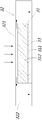
- FIG. 1 is a cross-sectional structural view of a fingerprint recognition module according to Embodiment 1 of the present invention.
- FIG. 2 is a cross-sectional structural diagram of a fingerprint identification module according to Embodiment 2 of the present invention.
- FIG. 3 is a schematic diagram of an explosion structure of a fingerprint identification module according to Embodiment 2 of the present invention.
- FIG. 4 is a cross-sectional structural diagram of a fingerprint identification module according to Embodiment 3 of the present invention.
- FIG. 5 is a cross-sectional structural diagram of a fingerprint identification module according to Embodiment 4 of the present invention.
- FIG. 6 is a schematic exploded view of an electrical mechanism and a reinforcing plate according to Embodiment 5 of the present invention.
- FIG. 7 is a cross-sectional structural view of a fingerprint identification module in a case where the circuit board does not exceed the receiving space of the fingerprint recognition chip according to Embodiment 5 of the present invention
- FIG. 8 is a cross-sectional structural view of a fingerprint recognition module in a case where a circuit board exceeds a receiving space of a fingerprint recognition chip according to Embodiment 5 of the present invention
- FIG. 9 is a cross-sectional structural view of a fingerprint recognition module in a case where a circuit board exceeds a receiving space of a fingerprint recognition chip according to Embodiment 5 of the present invention.
- FIG. 10 is a cross-sectional structural view of a fingerprint recognition module in a case where the circuit board and the substrate do not exceed the receiving space of the fingerprint recognition chip according to Embodiment 6 of the present invention
- FIG. 11 is a cross-sectional view showing the structure of a fingerprint recognition module in which the circuit board of the sixth embodiment of the present invention exceeds but the substrate does not exceed the receiving space of the fingerprint recognition chip;
- FIG. 12 is a cross-sectional structural view of a fingerprint recognition module in a case where the circuit board does not extend but the substrate exceeds the receiving space of the fingerprint recognition chip according to Embodiment 6 of the present invention
- FIG. 13 is a cross-sectional view showing the structure of a fingerprint recognition module in which the circuit board and the substrate are both outside the receiving space of the fingerprint recognition chip according to Embodiment 6 of the present invention.
- FIG. 1 shows a fingerprint identification module using a TSV (Through Silicon Via) package technology.
- the TSV package technology is a prior art and will not be described here.
- the fingerprint identification module includes:
- the electrical mechanism 11 and the mechanical mechanism 12 disposed on the periphery of the electrical mechanism 11 for dividing the pressure of the electrical mechanism 11 are provided.
- the mechanical mechanism 12 includes an upper cover 121 and a hollowed-out force transmitting member 122.
- the upper cover 121 and the force transmitting member 122 together form a receiving space.
- the bottom of the receiving space An opening that communicates with the hollowed middle portion.
- the electrical mechanism 11 includes a circuit board 111 and a fingerprint identification chip 112.
- the fingerprint identification chip 112 is configured to collect fingerprint image signals of a user.
- the circuit board 111 includes an extension portion (not shown in FIG. 1) and is disposed in the housing. In the connection portion in the space, the fingerprint recognition chip 112 is disposed in the accommodating space, and the signal output pad is located on the back surface, and is electrically connected to the signal input pad on the front surface of the connection portion by the solder 113.
- a support arm 1221 is disposed on an inner wall of the hollow portion of the force transmitting member 122, and the support arm 1221 forms a step with a top end surface of the force conducting member 122, and the receiving space is divided into the force conducting member.
- the upper cover 121 is disposed in the first receiving portion, and the fingerprint identification chip 112 and the The connecting portion is disposed in the second receiving portion, and a bottom end surface of the upper cover 121 and a top surface of the support arm 1221 are fixedly connected by glue.
- the top end surface of the fingerprint identification chip 112 and the bottom end surface of the upper cover 121 are fixedly connected by glue.
- the applied stress is pressed by the mechanical mechanism 12 to the fingerprint recognition module.
- the electrical mechanism 11 is only subjected to a small amount of pressure, which can reduce the mechanical damage probability of the electrical mechanism 11, and at the same time, the electrical mechanism 11 is subjected to The smaller the pressure, the smaller the deformation that occurs during use, and the more difficult the solder 113 between the fingerprint identification chip 112 and the connection portion is to loosen.
- a horizontal height of the bottom end surface of the connecting portion is higher than a horizontal height of the bottom end surface of the force transmitting member 122, that is, a gap 13 is left at the bottom of the connecting portion, and the gap 13 provides an elastic deformation allowance to the electrical mechanism 11,
- the electrical mechanism 11 is prevented from being in contact with other components after being deformed by pressure, and the electrical mechanism 11 can be protected during use.
- the circuit board 111 is preferably a flexible printed circuit board 111, which helps to reduce the overall thickness of the electrical mechanism 11, so that the gap 13 at the bottom of the electrical mechanism 11 can be designed without changing the thickness of the fingerprint recognition module. It is bigger.
- FIG. 2 and FIG. 3 show a fingerprint identification module using TSV (Through Silicon Via) packaging technology.
- TSV packaging technology is prior art and is no longer used here. Narration.
- the fingerprint identification module includes:
- the mechanical mechanism 22 includes an upper cover plate 221, a lower cover plate 222, and a centrally hollowed force transmitting member 223.
- the inner wall of the central portion of the force transmitting member 223 is provided with a support arm 2231, and the support arm 2231 is The top end surface and the bottom end surface of the force transmitting member 223 respectively form a step, and the receiving space is divided into a first receiving portion 24 closer to the top end surface of the force conducting member 223 than the supporting arm 2231 and compared with The support arm 2231 is closer to the third 26 receiving portion of the bottom end surface of the force conducting member 223, and the second receiving portion 25 between the first receiving portion 24 and the third receiving portion 26, the upper cover
- the plate 221 is disposed in the first receiving portion 24, the lower cover plate 222 is disposed in the third receiving portion 26, and the fingerprint identification chip 212 and the connecting portion 2111 are disposed in the second receiving portion
- the middle cover 25 and the upper cover 221 and the lower cover 222 close the second receiving portion 25.
- the bottom end surface of the upper cover plate 221 is fixedly connected to the upper surface of the support arm 2231, and the top end surface of the lower cover plate 222 is fixedly connected to the lower surface of the support arm 2231.
- the embodiment can prevent the reverse stress (the stress from the bottom to the top) from damaging the electrical mechanism 21.
- the electrical mechanism 21 includes a circuit board 211 and a fingerprint identification chip 212.
- the fingerprint recognition chip 212 is configured to collect a fingerprint image signal of the user.
- the circuit board 211 includes an extension portion 2112 and a connection disposed in the second receiving portion 25.
- the fingerprint recognition chip 212 is disposed in the second accommodating portion 25, and the signal output pad is located on the back surface, and is electrically connected to the signal input pad on the front surface of the connecting portion 2111 via the solder 213.
- the top end surface of the fingerprint recognition chip 212 and the bottom end surface of the upper cover 221 are fixedly connected by glue.
- the applied stress is pressed by the mechanical mechanism 22 to the fingerprint recognition module.
- the electrical mechanism 21 is only subjected to a small amount of pressure, which can reduce the mechanical damage probability of the electrical mechanism 21, and at the same time, the electrical mechanism 21 is subjected to The smaller the pressure, the smaller the deformation that occurs during use, and the less the solder 213 between the fingerprint identification chip 212 and the connecting portion 2111 is loosened.
- a gap 23 is left between the connecting portion 2111 and the lower cover 222, and the gap 23 provides an elastic deformation allowance to the electrical mechanism 21 to prevent the electrical mechanism 21 from being pressed and deformed and then touched with other components.
- the electrical mechanism 21 is protected during use.
- neither the fingerprint identification chip 212 nor the connecting portion 2111 is in contact with the inner wall of the hollow portion of the force transmitting member 223.
- the circuit board 211 is preferably a flexible printed circuit board 211, which helps to reduce the overall thickness of the electrical mechanism 21, so that the gap at the bottom of the electrical mechanism 21 can be designed without changing the thickness of the fingerprint recognition module. Bigger.
- FIG. 4 shows a fingerprint identification module using a plastic packaging technology.
- the plastic packaging technology is prior art and will not be described herein.
- the fingerprint identification module includes:
- the mechanical mechanism 32 in the embodiment is manufactured by a plastic packaging technology, and the upper cover 321 and the force transmitting member 322 in the mechanical mechanism 32 are a unitary structure.
- the electrical mechanism 31 includes a circuit board 311 and a fingerprint identification chip 312 disposed on the circuit board 311.
- the fingerprint identification chip 312 is configured to collect fingerprint image signals of the user.
- the fingerprint identification chip and the connecting portion may be in contact with the inner wall of the hollow portion of the force transmitting member, or may not be in contact with the inner wall of the hollow portion of the force transmitting member. This embodiment is not limited thereto.
- connection relationship between the components included in the electrical mechanism 31 and the connection relationship between the electrical mechanism 31 and the mechanical mechanism 32 are the same as those in the first embodiment and the second embodiment.
- the bottom of the electrical mechanism 31 is provided with a gap 33, and the suspension is disposed at the mechanical mechanism 32. It can be in the accommodating space formed.
- FIG. 5 shows a fingerprint identification module using a plastic packaging technology, which is different from the fingerprint identification module provided in the third embodiment.
- the mechanical mechanism 42 in this embodiment further includes a lower cover 421.
- the top end surface of the lower cover plate 421 and the lower end surface of the force transmitting member 422 are fixedly connected by glue to close the receiving space.
- the structure of the lower cover 421 which is increased in this embodiment as compared with the fourth embodiment can prevent the reverse stress (the stress from the bottom to the top) from damaging the electrical mechanism 41.
- the fingerprint identification module in the embodiment is also manufactured by using a plastic packaging technology, and is different from the first, second, third, and fourth embodiments of the circuit board of the embodiment.
- the reinforcing plate 523 is used as a reinforcing structure of the circuit board 511.
- the middle portion of the reinforcing plate 523 is hollowed out corresponding to the solder 513 on the back surface of the fingerprint identification chip 512, so as to ensure a gap is left in the bottom of the electrical connection of the electrical connection.
- the circuit board 511 may extend beyond the receiving space where the fingerprint identification chip 512 is located, or extend into the mechanical mechanism 52 and extend to the mechanical mechanism 52.
- the portion of the circuit board 511 can withstand the strain caused by the conduction of the pressure in the mechanical mechanism 52.
- the above structure can be flexibly adjusted according to the size of the circuit board 511. This embodiment is not limited thereto.
- circuit board 511 extends into the mechanical mechanism 52, it will be subjected to pressure, but since this part of the circuit board 511 is not electrically connected to the fingerprint identification chip 512 (the pad is not provided). Even if it is pressed, it does not cause the solder 513 between the fingerprint recognition chip 512 and the circuit board 511 to be loose.
- the fingerprint identification module in the embodiment is also manufactured by using a plastic packaging technology, and is different from the first, second, third, and fourth embodiments of the circuit board 612 of the embodiment.
- the electrical mechanism 61 further includes a substrate 613 which is disposed between the fingerprint identification chip 611 and the connection portion of the circuit board 612 as an electrical connection member.
- the circuit board 612 and the substrate 613 may extend beyond the receiving space where the fingerprint identifying chip is located, or extend beyond the receiving space of the fingerprint identifying chip 611 to the mechanical mechanism 62, and extend to the circuit board 612 in the mechanical mechanism 62.
- the portion of the substrate 613 can withstand the strain caused by the conduction of the pressure in the mechanical mechanism 62.
- the above structure can be flexibly adjusted according to the size of the circuit board 612 and the substrate 613. This embodiment is not limited thereto.
- the circuit board 612 and/or the substrate 613 although extending into the mechanical mechanism 62, are subject to pressure, but since this portion of the circuit board 612 and/or the substrate 613 is not associated with the fingerprint recognition chip.
- the 611 is electrically connected (no pad is provided), and even if it is pressed, the solder between the fingerprint chip 611 and the circuit board 612 and the substrate 613 is not loosened.
Landscapes
- Engineering & Computer Science (AREA)
- Physics & Mathematics (AREA)
- General Physics & Mathematics (AREA)
- Theoretical Computer Science (AREA)
- Microelectronics & Electronic Packaging (AREA)
- Multimedia (AREA)
- Computer Hardware Design (AREA)
- Human Computer Interaction (AREA)
- Power Engineering (AREA)
- Condensed Matter Physics & Semiconductors (AREA)
- Computer Security & Cryptography (AREA)
- General Health & Medical Sciences (AREA)
- Vascular Medicine (AREA)
- Health & Medical Sciences (AREA)
- Software Systems (AREA)
- General Engineering & Computer Science (AREA)
- Image Input (AREA)
- Measurement Of The Respiration, Hearing Ability, Form, And Blood Characteristics Of Living Organisms (AREA)
Abstract
Description
Claims (10)
- 一种指纹识别模组,其特征在于,所述指纹识别模组包括:电学机构和设置在所述电学机构外围用于分导所述电学机构所受压力的力学机构;所述力学机构包括上盖板和中部镂空的力传导部件,所述上盖板设置于所述力传导部件顶部与所述力传导部件共同组成一收容空间;所述电学机构包括电路板和指纹识别芯片,所述电路板包括延伸部和连接部,所述指纹识别芯片设置在所述收容空间内,并通过导电物与所述连接部电性连接;所述指纹识别芯片的顶部端面与所述上盖板的底部端面固定连接,所述连接部底部端面的水平高度高于所述力学机构底部端面的水平高度。
- 根据权利要求1所述的指纹识别模组,其特征在于,所述力传导部件中部镂空处的内壁上设有支撑臂,所述支撑臂与所述力传导部件的顶部端面形成一台阶,将所述收容空间分为靠近所述力传导部件顶部端面的第一收容部以及靠近所述力传导部件底部端面的第二收容部,所述上盖板设置于所述第一收容部中,所述指纹识别芯片和所述连接部设置在所述第二收容部中,所述上盖板的底部端面与所述支撑臂的上表面固定连接。
- 根据权利要求1所述的指纹识别模组,其特征在于,所述收容空间底部开口,所述力传导部件中部镂空处的内壁上设有支撑臂,所述力学机构还包括下盖板,所述上盖板的底部端面与所述支撑臂的上表面固定连接,所述下盖板的顶部端面与所述支撑臂的下表面固定连接,所述连接部与所述下盖板之间留有空隙。
- 根据权利要求3所述的指纹识别模组,其特征在于,所述支撑臂与所述力传导部件的顶部端面和底部端面分别形成一台阶,将所述收容空间分为相较所述支撑臂更靠近所述力传导部件顶部端面的第一收容部以及相较所述支撑臂更靠近所述力传导部件底部端面的第三收容部,以及位于所述第一收容部和所述第三收容部之间的第二收容部,所述上盖板设置于所述第一收容部中,所述下盖板设置在所述第三收容部中,所述指纹识别芯片和所述连接部设置在所述第二收容部中,且所述上盖板和所述下盖板封闭所述第二收容部。
- 根据权利要求1所述的指纹识别模组,其特征在于,所述上盖板和所述力传导部件为一体式结构。
- 根据权利要求5所述的指纹识别模组,其特征在于,所述力学机构还包括下盖板,所述下盖板的顶部端面与所述力学机构底部端面固定连接,所述下盖板封闭所述收容空间。
- 根据权利要求5所述的指纹识别模组,其特征在于,所述力学机构还包括补强板,所述补强板设置在所述电路板下方且中部镂空,所述镂空的位置与所述指纹识别芯片背面导电物的位置相对应。
- 根据权利要求7所述的指纹识别模组,其特征在于,所述电学机构还包括基板,所述基板设置在所述指纹识别芯片和所述连接部之间。
- 根据权利要求8所述的指纹识别模组,其特征在于,所述基板的边沿延伸至所述力学机构中。
- 根据权利要求7所述的指纹识别模组,其特征在于,所述电路板的连接部的边沿延伸至所述力学机构中。
Priority Applications (4)
| Application Number | Priority Date | Filing Date | Title |
|---|---|---|---|
| US15/570,777 US20180322326A1 (en) | 2015-05-08 | 2016-01-22 | Fingerprint identification module |
| KR1020177031362A KR20180025845A (ko) | 2015-05-08 | 2016-01-22 | 지문 인식 모듈 |
| JP2018509955A JP2018529158A (ja) | 2015-05-08 | 2016-01-22 | 指紋識別モジュール |
| EP16791903.4A EP3296921A4 (en) | 2015-05-08 | 2016-01-22 | FINGERPRINT IDENTIFICATION MODULE |
Applications Claiming Priority (2)
| Application Number | Priority Date | Filing Date | Title |
|---|---|---|---|
| CN201510233087.1A CN105046190B (zh) | 2015-05-08 | 2015-05-08 | 指纹识别模组 |
| CN201510233087.1 | 2015-05-08 |
Publications (1)
| Publication Number | Publication Date |
|---|---|
| WO2016180053A1 true WO2016180053A1 (zh) | 2016-11-17 |
Family
ID=54452719
Family Applications (1)
| Application Number | Title | Priority Date | Filing Date |
|---|---|---|---|
| PCT/CN2016/071701 WO2016180053A1 (zh) | 2015-05-08 | 2016-01-22 | 指纹识别模组 |
Country Status (6)
| Country | Link |
|---|---|
| US (1) | US20180322326A1 (zh) |
| EP (1) | EP3296921A4 (zh) |
| JP (1) | JP2018529158A (zh) |
| KR (1) | KR20180025845A (zh) |
| CN (1) | CN105046190B (zh) |
| WO (1) | WO2016180053A1 (zh) |
Cited By (1)
| Publication number | Priority date | Publication date | Assignee | Title |
|---|---|---|---|---|
| US10565425B2 (en) | 2018-02-06 | 2020-02-18 | Shenzhen GOODIX Technology Co., Ltd. | Under-screen biometric identification apparatus, biometric identification component and terminal device |
Families Citing this family (22)
| Publication number | Priority date | Publication date | Assignee | Title |
|---|---|---|---|---|
| CN105046190B (zh) * | 2015-05-08 | 2017-12-19 | 苏州迈瑞微电子有限公司 | 指纹识别模组 |
| CN105825165B (zh) * | 2015-11-20 | 2019-02-15 | 维沃移动通信有限公司 | 一种指纹识别模组、终端设备及装配方法 |
| CN106855938A (zh) * | 2015-12-08 | 2017-06-16 | 安徽昌硕光电子科技有限公司 | 一种指纹识别模块的结构 |
| CN105631444A (zh) * | 2016-03-17 | 2016-06-01 | 南昌欧菲生物识别技术有限公司 | 指纹识别模组及指纹识别模组组装方法 |
| CN106096596B (zh) * | 2016-08-16 | 2018-03-27 | 广东欧珀移动通信有限公司 | 指纹模组、指纹模组制作方法及移动终端 |
| ES2689917T3 (es) | 2016-08-16 | 2018-11-16 | Guangdong Oppo Mobile Telecommunications Corp., Ltd | Conjunto de entrada y terminal |
| CN107765107B (zh) * | 2016-08-18 | 2023-09-15 | 苏州迈瑞微电子有限公司 | 指纹识别模组灵敏度测试治具及测试方法 |
| CN106127195B (zh) | 2016-08-30 | 2017-11-17 | 广东欧珀移动通信有限公司 | 指纹模组、指纹模组制作方法及移动终端 |
| USD841651S1 (en) * | 2016-10-27 | 2019-02-26 | Apple Inc. | Electronic device |
| CN108280391B (zh) * | 2017-01-06 | 2021-04-30 | 致伸科技股份有限公司 | 指纹辨识模块 |
| CN107665335B (zh) * | 2017-09-18 | 2020-06-12 | 维沃移动通信有限公司 | 一种指纹识别模组和终端设备 |
| WO2019075698A1 (zh) * | 2017-10-19 | 2019-04-25 | 深圳市汇顶科技股份有限公司 | 模组结构、模组加工方法和终端设备 |
| CN107896259A (zh) * | 2017-10-31 | 2018-04-10 | 广东欧珀移动通信有限公司 | 指纹识别模组及其组装方法和电子装置 |
| CN110033072A (zh) * | 2018-01-11 | 2019-07-19 | 苏州迈瑞微电子有限公司 | 一种指纹u盘 |
| CN108493176B (zh) * | 2018-03-27 | 2020-07-10 | 浙江中正智能科技有限公司 | 一种指纹识别芯片装置及其制造方法 |
| WO2020133378A1 (zh) * | 2018-12-29 | 2020-07-02 | 深圳市汇顶科技股份有限公司 | 指纹识别装置和电子设备 |
| WO2020119289A1 (zh) | 2018-12-13 | 2020-06-18 | 深圳市汇顶科技股份有限公司 | 指纹识别装置和电子设备 |
| CN109791611B (zh) * | 2018-12-29 | 2021-04-23 | 深圳市汇顶科技股份有限公司 | 指纹识别装置和电子设备 |
| CN114640733B (zh) * | 2019-11-14 | 2023-06-27 | 华为技术有限公司 | 一种具有补强板的终端 |
| KR20210158459A (ko) * | 2020-06-23 | 2021-12-31 | 삼성디스플레이 주식회사 | 표시 장치 |
| CN111563047B (zh) * | 2020-07-13 | 2023-05-23 | 支付宝(杭州)信息技术有限公司 | 一种生物特征识别的攻击测试方法、装置及设备 |
| KR102310193B1 (ko) | 2021-07-20 | 2021-10-08 | 안덕기 | 대기오염 저감 개선 친환경 인공 나무 시스템 |
Citations (6)
| Publication number | Priority date | Publication date | Assignee | Title |
|---|---|---|---|---|
| WO2002008683A1 (en) * | 2000-07-26 | 2002-01-31 | Smith & Wesson Corp. | Authorization module and method for activating firearms |
| CN103699881A (zh) * | 2013-12-13 | 2014-04-02 | 深圳市汇顶科技股份有限公司 | 指纹识别装置和移动终端 |
| CN203535651U (zh) * | 2012-05-18 | 2014-04-09 | 苹果公司 | 用于指纹识别感测的装置、电子设备及移动设备 |
| CN203630794U (zh) * | 2013-12-13 | 2014-06-04 | 深圳市汇顶科技股份有限公司 | 指纹识别装置和移动终端 |
| CN105046190A (zh) * | 2015-05-08 | 2015-11-11 | 苏州迈瑞微电子有限公司 | 指纹识别模组 |
| CN204808352U (zh) * | 2015-04-23 | 2015-11-25 | 南昌欧菲生物识别技术有限公司 | 指纹识别模组 |
Family Cites Families (8)
| Publication number | Priority date | Publication date | Assignee | Title |
|---|---|---|---|---|
| JP2003086724A (ja) * | 2001-09-07 | 2003-03-20 | Sharp Corp | 半導体装置および指紋検知装置 |
| US7760921B2 (en) * | 2002-12-19 | 2010-07-20 | Casio Computer Co., Ltd. | Pressure activated fingerprint input apparatus |
| WO2004093005A1 (ja) * | 2003-04-15 | 2004-10-28 | Fujitsu Limited | 情報処理装置 |
| CA2529338A1 (en) * | 2003-06-12 | 2005-01-20 | Michael Arnouse | Personal identification and contact location and timing |
| TW200923722A (en) * | 2007-11-29 | 2009-06-01 | High Tech Comp Corp | Navigation input mechanism, electronic device including the same and method for switching mode thereof |
| US9152838B2 (en) * | 2012-03-29 | 2015-10-06 | Synaptics Incorporated | Fingerprint sensor packagings and methods |
| US9697409B2 (en) * | 2013-09-10 | 2017-07-04 | Apple Inc. | Biometric sensor stack structure |
| CN104050445B (zh) * | 2014-04-08 | 2018-10-16 | 南昌欧菲生物识别技术有限公司 | 指纹识别装置、指纹识别装置的封装方法和智能终端 |
-
2015
- 2015-05-08 CN CN201510233087.1A patent/CN105046190B/zh active Active
-
2016
- 2016-01-22 WO PCT/CN2016/071701 patent/WO2016180053A1/zh active Application Filing
- 2016-01-22 US US15/570,777 patent/US20180322326A1/en not_active Abandoned
- 2016-01-22 JP JP2018509955A patent/JP2018529158A/ja active Pending
- 2016-01-22 EP EP16791903.4A patent/EP3296921A4/en not_active Withdrawn
- 2016-01-22 KR KR1020177031362A patent/KR20180025845A/ko active Search and Examination
Patent Citations (6)
| Publication number | Priority date | Publication date | Assignee | Title |
|---|---|---|---|---|
| WO2002008683A1 (en) * | 2000-07-26 | 2002-01-31 | Smith & Wesson Corp. | Authorization module and method for activating firearms |
| CN203535651U (zh) * | 2012-05-18 | 2014-04-09 | 苹果公司 | 用于指纹识别感测的装置、电子设备及移动设备 |
| CN103699881A (zh) * | 2013-12-13 | 2014-04-02 | 深圳市汇顶科技股份有限公司 | 指纹识别装置和移动终端 |
| CN203630794U (zh) * | 2013-12-13 | 2014-06-04 | 深圳市汇顶科技股份有限公司 | 指纹识别装置和移动终端 |
| CN204808352U (zh) * | 2015-04-23 | 2015-11-25 | 南昌欧菲生物识别技术有限公司 | 指纹识别模组 |
| CN105046190A (zh) * | 2015-05-08 | 2015-11-11 | 苏州迈瑞微电子有限公司 | 指纹识别模组 |
Non-Patent Citations (1)
| Title |
|---|
| See also references of EP3296921A4 * |
Cited By (3)
| Publication number | Priority date | Publication date | Assignee | Title |
|---|---|---|---|---|
| US10565425B2 (en) | 2018-02-06 | 2020-02-18 | Shenzhen GOODIX Technology Co., Ltd. | Under-screen biometric identification apparatus, biometric identification component and terminal device |
| JP2020510887A (ja) * | 2018-02-06 | 2020-04-09 | シェンチェン グディックス テクノロジー カンパニー,リミテッド | アンダースクリーンバイオメトリクス認証装置、バイオメトリクス認証ユニット及び端末装置 |
| US11036960B2 (en) | 2018-02-06 | 2021-06-15 | Shenzhen GOODIX Technology Co., Ltd. | Under-screen biometric identification apparatus, biometric identification component and terminal device |
Also Published As
| Publication number | Publication date |
|---|---|
| JP2018529158A (ja) | 2018-10-04 |
| US20180322326A1 (en) | 2018-11-08 |
| KR20180025845A (ko) | 2018-03-09 |
| EP3296921A4 (en) | 2019-01-09 |
| CN105046190A (zh) | 2015-11-11 |
| EP3296921A1 (en) | 2018-03-21 |
| CN105046190B (zh) | 2017-12-19 |
Similar Documents
| Publication | Publication Date | Title |
|---|---|---|
| WO2016180053A1 (zh) | 指纹识别模组 | |
| US10551951B2 (en) | Input assembly with fingerprint identification chip arranged between a touch panel and flexible circuit board | |
| TWI558197B (zh) | 相機模組組件載具 | |
| US20170162620A1 (en) | Fingerprint recognition chip packaging structure and packaging method | |
| WO2015085786A1 (zh) | 指纹识别装置和移动终端 | |
| US9184519B2 (en) | Chip card connector with terminals disposed in openings on two sides of a partition part | |
| US20170234744A1 (en) | Mems force sensor and force sensing apparatus | |
| CN106407877B (zh) | 指纹辨识装置 | |
| CN107016328B (zh) | 指纹辨识装置 | |
| US9319772B2 (en) | Multi-floor type MEMS microphone | |
| US20150296305A1 (en) | Optimized back plate used in acoustic devices | |
| KR102022708B1 (ko) | 지문센서 모듈 및 이의 제조방법 | |
| WO2018033105A1 (en) | Fingerprint module, method for fabricating the same, and mobile terminal having the same | |
| WO2020020059A1 (zh) | 移动终端 | |
| KR20170016265A (ko) | 지문센서 패키지 및 이의 제조방법 | |
| WO2017201755A1 (zh) | 指纹模组及电子设备 | |
| CN105676953B (zh) | 一种具有指纹传感器封装结构的移动终端及其制备方法 | |
| CN105100569A (zh) | 摄像头模组及其第一线路板与第二线路板 | |
| US7315070B2 (en) | Fingerprint sensor package | |
| CN106203337A (zh) | 指纹识别模组及移动终端 | |
| CN105205483B (zh) | 指纹感测装置 | |
| WO2018149252A1 (zh) | 指纹识别组件及终端 | |
| US20150249891A1 (en) | Microphone package | |
| US20160134974A1 (en) | Lead frame-based chip carrier used in the fabrication of mems transducer packages | |
| US10037453B2 (en) | Capacitive fingerprint sensing module |
Legal Events
| Date | Code | Title | Description |
|---|---|---|---|
| 121 | Ep: the epo has been informed by wipo that ep was designated in this application |
Ref document number: 16791903 Country of ref document: EP Kind code of ref document: A1 |
|
| ENP | Entry into the national phase |
Ref document number: 20177031362 Country of ref document: KR Kind code of ref document: A |
|
| WWE | Wipo information: entry into national phase |
Ref document number: 15570777 Country of ref document: US |
|
| ENP | Entry into the national phase |
Ref document number: 2018509955 Country of ref document: JP Kind code of ref document: A |
|
| NENP | Non-entry into the national phase |
Ref country code: DE |