WO2016170759A1 - Socket structure for three-dimensional memory - Google Patents
Socket structure for three-dimensional memory Download PDFInfo
- Publication number
- WO2016170759A1 WO2016170759A1 PCT/JP2016/002025 JP2016002025W WO2016170759A1 WO 2016170759 A1 WO2016170759 A1 WO 2016170759A1 JP 2016002025 W JP2016002025 W JP 2016002025W WO 2016170759 A1 WO2016170759 A1 WO 2016170759A1
- Authority
- WO
- WIPO (PCT)
- Prior art keywords
- edge
- electrode
- electrodes
- socket region
- planar
- Prior art date
- Legal status (The legal status is an assumption and is not a legal conclusion. Google has not performed a legal analysis and makes no representation as to the accuracy of the status listed.)
- Ceased
Links
Images


Classifications
-
- H—ELECTRICITY
- H10—SEMICONDUCTOR DEVICES; ELECTRIC SOLID-STATE DEVICES NOT OTHERWISE PROVIDED FOR
- H10B—ELECTRONIC MEMORY DEVICES
- H10B41/00—Electrically erasable-and-programmable ROM [EEPROM] devices comprising floating gates
- H10B41/20—Electrically erasable-and-programmable ROM [EEPROM] devices comprising floating gates characterised by three-dimensional [3D] arrangements, e.g. with cells on different height levels
- H10B41/23—Electrically erasable-and-programmable ROM [EEPROM] devices comprising floating gates characterised by three-dimensional [3D] arrangements, e.g. with cells on different height levels with source and drain on different levels, e.g. with sloping channels
- H10B41/27—Electrically erasable-and-programmable ROM [EEPROM] devices comprising floating gates characterised by three-dimensional [3D] arrangements, e.g. with cells on different height levels with source and drain on different levels, e.g. with sloping channels the channels comprising vertical portions, e.g. U-shaped channels
-
- H—ELECTRICITY
- H10—SEMICONDUCTOR DEVICES; ELECTRIC SOLID-STATE DEVICES NOT OTHERWISE PROVIDED FOR
- H10B—ELECTRONIC MEMORY DEVICES
- H10B41/00—Electrically erasable-and-programmable ROM [EEPROM] devices comprising floating gates
- H10B41/30—Electrically erasable-and-programmable ROM [EEPROM] devices comprising floating gates characterised by the memory core region
- H10B41/35—Electrically erasable-and-programmable ROM [EEPROM] devices comprising floating gates characterised by the memory core region with a cell select transistor, e.g. NAND
-
- H—ELECTRICITY
- H10—SEMICONDUCTOR DEVICES; ELECTRIC SOLID-STATE DEVICES NOT OTHERWISE PROVIDED FOR
- H10B—ELECTRONIC MEMORY DEVICES
- H10B41/00—Electrically erasable-and-programmable ROM [EEPROM] devices comprising floating gates
- H10B41/50—Electrically erasable-and-programmable ROM [EEPROM] devices comprising floating gates characterised by the boundary region between the core region and the peripheral circuit region
-
- H—ELECTRICITY
- H10—SEMICONDUCTOR DEVICES; ELECTRIC SOLID-STATE DEVICES NOT OTHERWISE PROVIDED FOR
- H10B—ELECTRONIC MEMORY DEVICES
- H10B43/00—EEPROM devices comprising charge-trapping gate insulators
- H10B43/20—EEPROM devices comprising charge-trapping gate insulators characterised by three-dimensional [3D] arrangements, e.g. with cells on different height levels
- H10B43/23—EEPROM devices comprising charge-trapping gate insulators characterised by three-dimensional [3D] arrangements, e.g. with cells on different height levels with source and drain on different levels, e.g. with sloping channels
- H10B43/27—EEPROM devices comprising charge-trapping gate insulators characterised by three-dimensional [3D] arrangements, e.g. with cells on different height levels with source and drain on different levels, e.g. with sloping channels the channels comprising vertical portions, e.g. U-shaped channels
-
- H—ELECTRICITY
- H10—SEMICONDUCTOR DEVICES; ELECTRIC SOLID-STATE DEVICES NOT OTHERWISE PROVIDED FOR
- H10B—ELECTRONIC MEMORY DEVICES
- H10B43/00—EEPROM devices comprising charge-trapping gate insulators
- H10B43/30—EEPROM devices comprising charge-trapping gate insulators characterised by the memory core region
- H10B43/35—EEPROM devices comprising charge-trapping gate insulators characterised by the memory core region with cell select transistors, e.g. NAND
-
- H—ELECTRICITY
- H10—SEMICONDUCTOR DEVICES; ELECTRIC SOLID-STATE DEVICES NOT OTHERWISE PROVIDED FOR
- H10B—ELECTRONIC MEMORY DEVICES
- H10B43/00—EEPROM devices comprising charge-trapping gate insulators
- H10B43/50—EEPROM devices comprising charge-trapping gate insulators characterised by the boundary region between the core and peripheral circuit regions
-
- H—ELECTRICITY
- H10—SEMICONDUCTOR DEVICES; ELECTRIC SOLID-STATE DEVICES NOT OTHERWISE PROVIDED FOR
- H10B—ELECTRONIC MEMORY DEVICES
- H10B63/00—Resistance change memory devices, e.g. resistive RAM [ReRAM] devices
- H10B63/80—Arrangements comprising multiple bistable or multi-stable switching components of the same type on a plane parallel to the substrate, e.g. cross-point arrays
- H10B63/84—Arrangements comprising multiple bistable or multi-stable switching components of the same type on a plane parallel to the substrate, e.g. cross-point arrays arranged in a direction perpendicular to the substrate, e.g. 3D cell arrays
-
- H—ELECTRICITY
- H10—SEMICONDUCTOR DEVICES; ELECTRIC SOLID-STATE DEVICES NOT OTHERWISE PROVIDED FOR
- H10N—ELECTRIC SOLID-STATE DEVICES NOT OTHERWISE PROVIDED FOR
- H10N70/00—Solid-state devices having no potential barriers, and specially adapted for rectifying, amplifying, oscillating or switching
- H10N70/011—Manufacture or treatment of multistable switching devices
-
- H—ELECTRICITY
- H10—SEMICONDUCTOR DEVICES; ELECTRIC SOLID-STATE DEVICES NOT OTHERWISE PROVIDED FOR
- H10W—GENERIC PACKAGES, INTERCONNECTIONS, CONNECTORS OR OTHER CONSTRUCTIONAL DETAILS OF DEVICES COVERED BY CLASS H10
- H10W20/00—Interconnections in chips, wafers or substrates
- H10W20/01—Manufacture or treatment
-
- H—ELECTRICITY
- H10—SEMICONDUCTOR DEVICES; ELECTRIC SOLID-STATE DEVICES NOT OTHERWISE PROVIDED FOR
- H10W—GENERIC PACKAGES, INTERCONNECTIONS, CONNECTORS OR OTHER CONSTRUCTIONAL DETAILS OF DEVICES COVERED BY CLASS H10
- H10W20/00—Interconnections in chips, wafers or substrates
- H10W20/40—Interconnections external to wafers or substrates, e.g. back-end-of-line [BEOL] metallisations or vias connecting to gate electrodes
- H10W20/41—Interconnections external to wafers or substrates, e.g. back-end-of-line [BEOL] metallisations or vias connecting to gate electrodes characterised by their conductive parts
- H10W20/42—Vias, e.g. via plugs
Definitions
- the present disclosure relates to socket configurations for three-dimensional memories, and in particular to improving the area efficiency of sockets for three-dimensional memories.
- Solid-state memory can be used for long or short term storage of program instructions and data in connection with computing devices.
- Memory density, access speed, and reliability are all important considerations in designing solid-state memory.
- Recent solid-state memory designs have used three-dimensional architectures. Such designs can increase memory density.
- ReRAM resistive random access memory
- PCRAM phase-change random access memory
- signal lines including bit lines (BL) and word lines (WL), extend between socket regions on a periphery of the memory structure, and the memory array itself. More particularly, a first socket region on a first side of the memory array can include electrodes or contacts associated with the bit lines, and a second socket region on a second side of the memory array can include electrodes or contacts associated with the word lines. In other configurations, socket regions on first and second opposing sides of the memory array can be associated with bit lines, and socket regions on third and fourth opposing sides of the memory array can be associated with word lines. As the number of memory cells included in the memory array is increased, there is a corresponding increase in the number of signal lines (i.e. bit lines and/or word lines).
- signal lines i.e. bit lines and/or word lines
- the area of the memory structure occupied by the socket regions becomes increasingly large as compared to an area of the memory array. This problem is exacerbated by decreases in the size of memory cells and in the size of memory cell pitch, and increases in the density of the memory array.
- the area of the memory structure occupied by socket regions also increases relative to the area of the memory structure occupied by the memory array as the number of decks or layers within the memory structure increases. More particularly, in a conventional socket arrangement, different decks or layers, corresponding to different horizontal electrodes, are disposed in a staircase type arrangement. These different layers are accessed by vertical conductors. As a result, the size of the socket area must be increased in order to accommodate an increased number of horizontal electrodes. That is, the number of “stairs” in the “staircase” must be increased, which for a given electrode contact size results in a proportional increase in the length of the socket region in a direction extending away from the memory array.
- the size of a contact established between a horizontal electrode and a vertical conductor is constrained by various factors. For example, a minimum contact area needs to be maintained in order to provide a suitable electrical contact and thus a suitably low electrical resistance.
- the ability to align a vertical conductor with a desired contact area can be limited by manufacturing tolerances, thus requiring some minimum contact area margin. Therefore, the proportion of the total area occupied by connection or socket regions tends to become increasingly large as memory cell area density increases.
- memory cells can be densely packed within the memory array. However, as the number of memory cells within a given area increases, the proportion of the overall area of the memory structure that is occupied by socket regions, rather than by memory cells, increases.
- Embodiments of the present disclosure provide socket structures for three-dimensional memories that are configured to efficiently provide connections to memory cells within the memory array.
- individual memory cells are accessed by selectively energizing bit lines and word lines.
- Bit lines and word lines are accessed through the bit line socket region or regions and word line socket region or regions respectively.
- the area of the bit line socket region or word line socket region also increases.
- Embodiments of the present disclosure provide for a socket region comprising a staircase contact region that requires less area than in a conventional arrangement otherwise configured similarly.
- a length factor dependent on a number of decks or horizontal electrodes can be decreased as compared to the conventional configuration.
- a staircase type contact arrangement in accordance with embodiments of the present disclosure allows for an alignment margin applied to connecting conductors to be reduced as compared to conventional arrangements. Moreover, embodiments of the present disclosure allow contacts to electrically connect to both a top surface and an edge surface of a horizontal electrode. As a result, electrical performance, such as suitably low electrical resistance, can be maintained, even while the contact area available on a top surface of the horizontal electrodes is reduced as compared to conventional configurations.
- the edge of the dielectric layers interposed between adjacent horizontal or planar electrodes is sloped.
- a top of the edge of a dielectric layer can extend from a point corresponding to an edge of a first horizontal electrode to a point on a second horizontal electrode that is between an edge of the second horizontal electrode and a point on the second horizontal electrode in a first dimension equal to the furthest extent of the first electrode in the first dimension.
- Methods in accordance with embodiments of the present disclosure provide a staircase type contact arrangement that allows the corresponding socket region to have a reduced area as compared to a staircase contact configured according to conventional arrangements. According to such methods, a pullback process is used to successively reveal planar electrodes as steps in a staircase. Dielectric layers disposed between adjacent planar electrodes are etched such that at least a portion of an edge of each dielectric layer lies in an area between an edge of an underlying horizontal electrode and an edge of an overlying horizontal electrode. In accordance with at least some embodiments, the edge of each dielectric layer is sloped. Methods in accordance with embodiments of the present disclosure can additionally include providing connecting conductors that contact both a portion of a top surface of an electrode and a portion of an edge surface of the electrode.
- Adjacent horizontal electrodes included in the plurality of horizontal electrodes are separated from one another in the z dimension by at least one of the dielectric layers included in the plurality of dielectric layers.
- the horizontal electrodes move in at least a first direction along the z dimension, extend from the memory array area to the first socket region by a greater amount, forming a staircase structure.
- An edge of a dielectric layer disposed between a first horizontal electrode and a second horizontal electrode is located between an edge of the first horizontal electrode and an edge of the second horizontal electrode.
- each horizontal electrode of the plurality of horizontal electrodes includes a portion that is not covered by a dielectric layer such that each of the horizontal electrodes is accessible along one more lines that are parallel to the z dimension.
- a method for forming a staircase contact socket region comprises providing a stack having a plurality of planar electrodes and a plurality of insulating layers, in which adjacent planar electrodes are separated from one another by an insulating layer.
- a mask is placed on the stack, and a first portion of a first insulating layer not under the mask is etched to expose a first portion of a first planar electrode in the plurality of planar electrodes.
- the mask is then pulled back.
- the method further includes pulling back the mask, etching a second portion of the first insulating layer, etching the first portion of the first planar electrode, and etching a first portion of a second insulating layer.
- the edge of the second insulating layer formed by the etching is sloped and extends from an edge of the first planar electrode to between the edge of the first planar electrode and an edge of the second planar electrode.
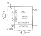
- Fig. 1 is a perspective view of an exemplary three-dimensional memory structure.
- Fig. 2 depicts areas of a three dimensional memory structure in plan view.
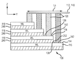
- Fig. 3 depicts a prior art three dimensional memory structure in elevation.
- Fig. 4 depicts the prior art three dimensional memory structure of Fig. 3 in plan view.
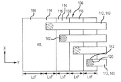
- Fig. 5 depicts a three dimensional memory structure in accordance with embodiments of the present disclosure in elevation.
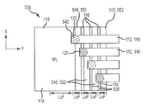
- Fig. 6 depicts the three dimensional memory structure of Fig. 5 in plan view.
- Fig. 7 is a graph depicting the area efficiency of an example three-dimensional memory structure in accordance with embodiments of the present invention as compared to the area efficiency of a reference three-dimensional memory structure.
- Fig. 1 depicts an example three-dimensional memory structure 100. More particularly, a three-dimensional memory structure 100 in the form of a vertical memory array is depicted.
- the memory structure 100 includes a plurality of bit lines 104 that are electrically connected to the ends of vertical memory elements 108.
- the memory structure 100 also includes a plurality of word lines 112 and a plurality of horizontal or planar electrodes 116. Each word line 112 is connected to a top surface 114 of a horizontal electrode or deck 116, either directly or through a connecting conductor 120.
- the horizontal electrodes 116 are generally disposed within planes extending in the x and y dimensions.
- the number of word line contacts or bits 140 is, in this example, equal to the number of bit lines 112.
- the area encompassed by the word line socket region 136 is shown as a projection, as the connecting portions 138 of the horizontal electrodes 116 electrically connected to a connecting conductor 120 at a contact 142 are disposed in a staircase type arrangement, in which the connecting portions 138 of the different horizontal electrodes or decks 116 are disposed at different distances from the memory array area 128.
- the number of bit lines 108 and/or word lines 112 increases.
- the number of word lines 112 is greater than the number of bit lines 104, which generally supports a high density memory array area 128, by allowing for an increased number of horizontal electrodes or decks 116.
- a three-dimensional memory structure such as the example prior art memory structure 100, has memory cells 124 disposed in three-dimensions
- the bit line 132 and word line 136 socket regions require a certain amount of area within a plane parallel to the horizontal electrodes 116 in which to complete the connections. The result is that, as the number of memory cells 124 increases, and in particular as the number of horizontal electrodes or decks 116 increases, the proportion of the total area of the memory structure occupied by the bit line 132 and word line 136 socket regions becomes increasingly large.
- the length L s_word of the word line socket region 136 increases as the number (n) of horizontal electrodes 116 increases, in order to provide the connecting conductors 120 access to the horizontal electrodes 116, which are disposed in a staircase contact arrangement. Therefore, as the number of decks or horizontal electrodes 116 is increased, the area density of the memory array 128 increases, and the area occupied by the word line socket region or regions 136 also increases. Similarly, as the number (m) of bit lines 104 increases, the area occupied by the bit line socket region or regions 132 increases.
- each horizontal electrode 116 is separated from an adjacent horizontal electrode 116 by a dielectric or insulating layer 248.
- Each insulating layer 248 has an end surface 252 that is vertical (i.e. is orthogonal or at 90 degrees to the top surface 114 of the horizontal electrode 116, and parallel to the z dimension) and that extends no further in a y direction than the horizontal electrode 116 directly above the insulating layer 248. Accordingly, a portion of the planar top surface 114 of each horizontal electrode 116 is available as a contact region 138 in which a contact 142 with a corresponding connecting conductor 120 can be formed.
- the alignment margin or spacing factor that must be maintained in the y dimension between adjacent connecting conductors 120, and more particularly between connecting conductors 120 electrically connected to a selected horizontal electrode 116 and the horizontal electrodes 116 on either side of the selected horizontal electrode 116 is relatively large, resulting in a spacing, given by LnF, that is correspondingly large.
- Fig. 5 depicts a portion of a three-dimensional memory structure, such as the memory structure 100 illustrated in Fig. 1, encompassing a word line socket region 536, configured in accordance with embodiments of the present disclosure in elevation, from a line of sight taken along the x axis.
- Fig. 6 depicts the word line socket region 536 portion of the memory structure 100 shown in Fig. 5 in plan view, from a line of sight taken along the z axis.
- the socket region 536 is similar to a conventional socket region 136 in that the ends of the planar electrodes 116 are disposed in a staircase type arrangement, in which the electrodes extend further in the y dimension the lower they are in the stack.
- each planar electrode 116 is separated from an adjacent electrode by an insulating or dielectric layer 548 interposed between the adjacent dielectric layers.
- the spacing between vertical or connecting conductors 120 has been reduced in the y direction. That is, the alignment margin or length factor has been decreased as compared to the prior art configuration illustrated in Figs. 3 and 4.
- the alignment margin can be zero.
- the alignment margin can be negative, such that the connecting conductors 120 overlap with one another in the y dimension, so long as they are separated from one another in the x dimension.
- embodiments of the present disclosure allow the spacing between the centerlines of the vertical conductors 120 to be reduced as compared to the spacing between vertical conductors 120 according to the prior art. Accordingly, for a given number of decks 116, and all other factors being equal, the length of a socket region 536 configured in accordance with embodiments of the present disclosure will be shorter than the socket length of a socket region 136 configured in accordance with the prior art. This reduced spacing is made possible by the tapered or sloped configuration of the edge surface 552 of the dielectric layers 548 between adjacent horizontal electrodes 116.
- the edge 552 corresponding to or including the farthest extent in the y dimension of a dielectric layer 548 extends to a point between the furthest extent in the y dimension of the horizontal electrode 116 (e.g., horizontal electrodes 116a) directly above the dielectric layer 548 and the horizontal electrode 116 (e.g., horizontal electrode 116b) directly below the dielectric layer 548.
- the top surface 114 of the underlying horizontal electrode 116 between the edge surface 554 of the horizontal electrode 116a and the edge surface 554 of the overlying horizontal electrode 116 is partially covered by the dielectric layer 548.
- each dielectric layer 548 is sloped, such that it extends from a point corresponding to an end of a bottom surface of a horizontal electrode 116 that overlies the dielectric layer 548 to a point that is towards, but not as far as, the edge surface 554 of the underlying horizontal electrode 116. Accordingly, an uncovered portion 538 of the top surface 114 of the underlying horizontal electrode 116 that is available as a contact area 542 is reduced as compared to a configuration in which the edge of the dielectric layer is vertical.
- an area of the top surface 114 of an underlying horizontal electrode 116 that is not overlapped by an overlaying horizontal electrode 116 is partially covered by the sloped end portion 552 of the intervening dielectric layer 548.
- alignment tolerances, and thus an alignment margin requirement is reduced as compared to the conventional configuration, or is eliminated entirely.
- a vertical conductor 120 that is misaligned will be prevented from contacting the horizontal electrode 116 directly below a target horizontal electrode 116 by the dielectric layer 548 underlying the target horizontal electrode 116. That is, over at least some range, the effect of a misaligned vertical conductor 120 can be obviated.
- the length of the socket region L s of embodiments of the present invention is reduced as compared to a conventional arrangement having vertical dielectric layer edges.
- an edge portion 554 of the target horizontal electrode 116 is available as a portion of the contact area 542. Therefore, electrical performance, including but not limited to a suitably low electrical resistance, between a horizontal electrode 116 and an associated vertical conductor 120 can be maintained, even if the area of the uncovered portion of the top surface 538 is reduced as compared to conventional configurations.
- the vertical conductor is sized and aligned such that it contacts a portion of a dielectric layer 548 on either side of a target horizontal electrode 116.
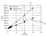
- Fig. 7 is a graph comparing the length of a word line socket region 136 configured according to conventional techniques (plot 704) to the length of a word line socket region 536 configured in accordance with embodiments of the present disclosure (plot 708). More particularly, the length (L s ) of the word line socket regions 136, 536 for three-dimensional memory structures having differing numbers of layers 116 are depicted. In this example, for a given constant length factor, and a given half pitch of cell area, it can be seen that the length of a word line socket region 536 constructed in accordance with embodiments of the present disclosure increases with the number of decks (n) at a rate that is less than the rate that the length of the word line socket region 136 constructed in accordance with conventional techniques increases. Accordingly, a reduction in size of a memory structure can be achieved.
- the area efficiency of a three-dimensional memory structure utilizing a word line socket region 536 configured in accordance with embodiments of the present disclosure can be greater than that of a conventional arrangement.
- the area efficiency of a three-dimensional memory structure can be evaluated as the ratio of the area of the memory array to the area of the memory array plus the area of the socket regions. More particularly, the area efficiency can be expressed as follows: where Eff is the area efficiency of the memory structure, A c is the area of the memory cell area, A first_socket_region is the area of the first socket region, A second_socket_region is the area of the second socket region, and A s is the total area of the bit line and word line socket regions. For example, with reference to Fig.
- the area efficiency is equal to the area of the memory array area 128 divided by the area equal to the memory array area 128 plus the area of the bit line socket region 132 plus the area of the word line socket region 136, 536 where all of the areas are in a plane that is generally parallel to the horizontal electrodes or decks 116. Accordingly, where a socket region encompasses a staircase contact region, the area of that socket region is given by the projection of the region onto a horizontal plane.
- a method for providing a socket region within a reduced area as compared to conventional techniques or configurations is provided.
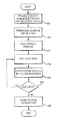
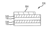
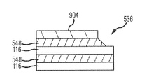
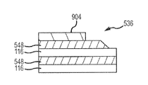
- Fig. 8 presents a flowchart illustrating process steps of such a method, and the socket structure 536 at different stages during performance of the process steps is illustrated in elevation in Figs. 9A-9D.
- the method can include providing a stack of planar or horizontal electrodes 116, with each planar electrode 116 separated from a neighboring planar electrode 116 by a dielectric layer 548 (step 804).
- a mask layer can then be formed over a top dielectric layer 548, such that the mask leaves a portion of the underlying dielectric layer uncovered (step 808).
- FIG. 9A illustrates the socket region 536 after the addition of the mask 904.
- the exposed portion of the dielectric layer 548 can then be etched (step 812).
- the socket region 536 after the initial step of etching is depicted in Fig. 9B.
- the mask 904 can then be pulled back (step 816).
- the socket region 536 after pulling back the mask 904 is depicted in Fig. 9C.
- the planar electrode 116 exposed in the previous etching step, and a next dielectric layer 548 can be etched, while the upper dielectric layer 548 can be further etched (step 820).
- the socket region 536 after completion of step 820 is shown in Fig. 9D. This pullback process can be continued until a portion of the last planar electrode 116 is exposed.
- the dielectric layers 548 are tapered, to create a sloped surface, rather than etched at a right angle to a top surface of an underlying planar electrode 116.
- the amount by which a dielectric layer 548 is “pulled back” can be less than the amount by which the overlying planar electrode 116 is “pulled back”.
- a determination can be made as to whether the last planar electrode 116 has been reached. If not, the process may return to step 816.
- vertical or connecting conductors 120 can be formed, such that at least one vertical conductor 120 is connected to each planar electrode 116 (step 828).
- the contact area 552 between a planar electrode 116 and an associated vertical conductor 120 encompasses portions of a top surface 114 of the horizontal electrode 116 as well as a portion of the edge surface 554 of the planar electrode 116.
- the provision of dielectric layers 548 having sloped edges 532 prevents a vertical conductor 120 from electrically contacting a planar electrode 116 below a target planar electrode 116. Therefore, the alignment margin required for a given manufacturing tolerance can be reduced as compared to a conventional staircase type contact configuration.
- a socket region configuration that can occupy a reduced area as compared to conventional socket region arrangements in connection with a three-dimensional memory structure
- embodiments of the present disclosure are not limited to use in connection with such structures.
- a socket region as disclosed herein can be utilized in connection with any electrical structure in which contacts are disposed in a staircase type arrangement.
- embodiments of the present disclosure provide a configuration in which an alignment margin can be reduced with respect to electrical contacts disposed in a staircase type arrangement.
Landscapes
- Engineering & Computer Science (AREA)
- Manufacturing & Machinery (AREA)
- Semiconductor Memories (AREA)
Priority Applications (2)
| Application Number | Priority Date | Filing Date | Title |
|---|---|---|---|
| JP2017552102A JP6788607B2 (ja) | 2015-04-24 | 2016-04-14 | 階段型コンタクトソケット領域を形成する方法 |
| KR1020177029491A KR20170141665A (ko) | 2015-04-24 | 2016-04-14 | 3차원 메모리를 위한 소켓 구조물 |
Applications Claiming Priority (2)
| Application Number | Priority Date | Filing Date | Title |
|---|---|---|---|
| US14/695,835 | 2015-04-24 | ||
| US14/695,835 US9515125B2 (en) | 2015-04-24 | 2015-04-24 | Socket structure for three-dimensional memory |
Publications (1)
| Publication Number | Publication Date |
|---|---|
| WO2016170759A1 true WO2016170759A1 (en) | 2016-10-27 |
Family
ID=55863153
Family Applications (1)
| Application Number | Title | Priority Date | Filing Date |
|---|---|---|---|
| PCT/JP2016/002025 Ceased WO2016170759A1 (en) | 2015-04-24 | 2016-04-14 | Socket structure for three-dimensional memory |
Country Status (4)
| Country | Link |
|---|---|
| US (3) | US9515125B2 (enExample) |
| JP (1) | JP6788607B2 (enExample) |
| KR (1) | KR20170141665A (enExample) |
| WO (1) | WO2016170759A1 (enExample) |
Cited By (3)
| Publication number | Priority date | Publication date | Assignee | Title |
|---|---|---|---|---|
| WO2019099103A1 (en) * | 2017-11-15 | 2019-05-23 | Sandisk Technologies Llc | Three-dimensional memory device with thickened word lines in terrace region and method of making thereof |
| US10453854B2 (en) | 2017-11-15 | 2019-10-22 | Sandisk Technologies Llc | Three-dimensional memory device with thickened word lines in terrace region |
| US10461163B2 (en) | 2017-11-15 | 2019-10-29 | Sandisk Technologies Llc | Three-dimensional memory device with thickened word lines in terrace region and method of making thereof |
Families Citing this family (5)
| Publication number | Priority date | Publication date | Assignee | Title |
|---|---|---|---|---|
| US9478556B2 (en) | 2014-09-11 | 2016-10-25 | Kabushiki Kaisha Toshiba | Semiconductor memory device |
| KR102536261B1 (ko) | 2015-12-18 | 2023-05-25 | 삼성전자주식회사 | 3차원 반도체 장치 |
| US9767901B1 (en) * | 2016-08-24 | 2017-09-19 | Hewlett Packard Enterprise Development Lp | Circuits having selector devices with different I-V responses |
| US10777566B2 (en) * | 2017-11-10 | 2020-09-15 | Macronix International Co., Ltd. | 3D array arranged for memory and in-memory sum-of-products operations |
| US11222695B2 (en) * | 2019-11-15 | 2022-01-11 | Micron Technology, Inc. | Socket design for a memory device |
Citations (2)
| Publication number | Priority date | Publication date | Assignee | Title |
|---|---|---|---|---|
| EP1434258A2 (en) * | 2002-12-24 | 2004-06-30 | STMicroelectronics S.r.l. | MOS device and a process for manufacturing MOS devices using a dual-polysilicon layer technology with side contact |
| US20070252201A1 (en) * | 2006-03-27 | 2007-11-01 | Masaru Kito | Nonvolatile semiconductor memory device and manufacturing method thereof |
Family Cites Families (7)
| Publication number | Priority date | Publication date | Assignee | Title |
|---|---|---|---|---|
| KR101065140B1 (ko) * | 2008-03-17 | 2011-09-16 | 가부시끼가이샤 도시바 | 반도체 기억 장치 |
| JP2010027870A (ja) * | 2008-07-18 | 2010-02-04 | Toshiba Corp | 半導体記憶装置及びその製造方法 |
| JP5380190B2 (ja) * | 2009-07-21 | 2014-01-08 | 株式会社東芝 | 不揮発性半導体記憶装置及びその製造方法 |
| KR101559958B1 (ko) * | 2009-12-18 | 2015-10-13 | 삼성전자주식회사 | 3차원 반도체 장치의 제조 방법 및 이에 따라 제조된 3차원 반도체 장치 |
| JP2011211039A (ja) * | 2010-03-30 | 2011-10-20 | Toshiba Corp | 記憶装置及びその製造方法 |
| US8885382B2 (en) * | 2012-06-29 | 2014-11-11 | Intel Corporation | Compact socket connection to cross-point array |
| JP2015056452A (ja) * | 2013-09-10 | 2015-03-23 | 株式会社東芝 | 半導体記憶装置及びその製造方法 |
-
2015
- 2015-04-24 US US14/695,835 patent/US9515125B2/en not_active Expired - Fee Related
-
2016
- 2016-04-14 KR KR1020177029491A patent/KR20170141665A/ko not_active Abandoned
- 2016-04-14 WO PCT/JP2016/002025 patent/WO2016170759A1/en not_active Ceased
- 2016-04-14 JP JP2017552102A patent/JP6788607B2/ja not_active Expired - Fee Related
- 2016-11-03 US US15/342,819 patent/US9728722B2/en not_active Expired - Fee Related
-
2017
- 2017-06-14 US US15/623,030 patent/US9935266B2/en active Active
Patent Citations (2)
| Publication number | Priority date | Publication date | Assignee | Title |
|---|---|---|---|---|
| EP1434258A2 (en) * | 2002-12-24 | 2004-06-30 | STMicroelectronics S.r.l. | MOS device and a process for manufacturing MOS devices using a dual-polysilicon layer technology with side contact |
| US20070252201A1 (en) * | 2006-03-27 | 2007-11-01 | Masaru Kito | Nonvolatile semiconductor memory device and manufacturing method thereof |
Cited By (3)
| Publication number | Priority date | Publication date | Assignee | Title |
|---|---|---|---|---|
| WO2019099103A1 (en) * | 2017-11-15 | 2019-05-23 | Sandisk Technologies Llc | Three-dimensional memory device with thickened word lines in terrace region and method of making thereof |
| US10453854B2 (en) | 2017-11-15 | 2019-10-22 | Sandisk Technologies Llc | Three-dimensional memory device with thickened word lines in terrace region |
| US10461163B2 (en) | 2017-11-15 | 2019-10-29 | Sandisk Technologies Llc | Three-dimensional memory device with thickened word lines in terrace region and method of making thereof |
Also Published As
| Publication number | Publication date |
|---|---|
| US20160315121A1 (en) | 2016-10-27 |
| US20170077399A1 (en) | 2017-03-16 |
| US9728722B2 (en) | 2017-08-08 |
| US9515125B2 (en) | 2016-12-06 |
| JP6788607B2 (ja) | 2020-11-25 |
| US20170288141A1 (en) | 2017-10-05 |
| JP2018513559A (ja) | 2018-05-24 |
| KR20170141665A (ko) | 2017-12-26 |
| US9935266B2 (en) | 2018-04-03 |
Similar Documents
| Publication | Publication Date | Title |
|---|---|---|
| US9935266B2 (en) | Socket structure for three-dimensional memory | |
| US20250233114A1 (en) | Apparatus for non-volatile random access memory stacks | |
| US9691820B2 (en) | Block architecture for vertical memory array | |
| KR102024723B1 (ko) | 3차원 반도체 장치 | |
| TWI580006B (zh) | 三維半導體裝置的內連線結構 | |
| US20140106569A1 (en) | Method of fabricating three-dimensional semiconductor device and three-dimensional semiconductor device fabricated using the same | |
| US8482133B2 (en) | Semiconductor package | |
| US20110316072A1 (en) | Semiconductor memory devices including asymmetric word line pads | |
| US8946892B2 (en) | Semiconductor package | |
| KR20090128779A (ko) | 반도체 장치 및 그 제조 방법 | |
| US9190404B2 (en) | Semiconductor device and method of fabricating the same | |
| WO2018119987A1 (en) | Dual in-line memory modules and connectors for increased system performance | |
| US8614507B2 (en) | Semiconductor devices having lower and upper interconnection structures that exhibit reduced coupling | |
| CN102881317B (zh) | 三维存储器阵列 | |
| US6667505B2 (en) | Semiconductor device having a plurality of capacitors aligned at regular intervals | |
| US11271154B2 (en) | Magnetic tunnel junction (MTJ) device | |
| US20250220930A1 (en) | Integrated circuits including polysilicon resistors | |
| US20170069567A1 (en) | Memory structure | |
| WO2020121491A1 (ja) | 半導体モジュール及びその製造方法 | |
| US10477674B2 (en) | Uniformization of parasitic capacitance around wiring of a circuit substrate | |
| CN112670295A (zh) | 三维存储器的制造方法及三维存储器 | |
| US20250194011A1 (en) | Printed circuit board and semiconductor package having the same | |
| US12087716B2 (en) | Techniques for positioning bond pads of microelectronic devices and related microelectronic devices, methods, and systems | |
| US20260090341A1 (en) | Semiconductor dies and semiconductor wafers for detecting misalignment of chip bonding pads | |
| KR20250106650A (ko) | 폴리실리콘 저항들을 포함하는 집적 회로들 |
Legal Events
| Date | Code | Title | Description |
|---|---|---|---|
| 121 | Ep: the epo has been informed by wipo that ep was designated in this application |
Ref document number: 16719937 Country of ref document: EP Kind code of ref document: A1 |
|
| ENP | Entry into the national phase |
Ref document number: 2017552102 Country of ref document: JP Kind code of ref document: A |
|
| ENP | Entry into the national phase |
Ref document number: 20177029491 Country of ref document: KR Kind code of ref document: A |
|
| NENP | Non-entry into the national phase |
Ref country code: DE |
|
| 122 | Ep: pct application non-entry in european phase |
Ref document number: 16719937 Country of ref document: EP Kind code of ref document: A1 |