WO2016170663A1 - イオン液体を用いた試料の観察方法及び標本の生産方法 - Google Patents
イオン液体を用いた試料の観察方法及び標本の生産方法 Download PDFInfo
- Publication number
- WO2016170663A1 WO2016170663A1 PCT/JP2015/062461 JP2015062461W WO2016170663A1 WO 2016170663 A1 WO2016170663 A1 WO 2016170663A1 JP 2015062461 W JP2015062461 W JP 2015062461W WO 2016170663 A1 WO2016170663 A1 WO 2016170663A1
- Authority
- WO
- WIPO (PCT)
- Prior art keywords
- ionic liquid
- sample
- observation
- producing
- substrate
- Prior art date
- Legal status (The legal status is an assumption and is not a legal conclusion. Google has not performed a legal analysis and makes no representation as to the accuracy of the status listed.)
- Ceased
Links
Images





Classifications
-
- H—ELECTRICITY
- H01—ELECTRIC ELEMENTS
- H01J—ELECTRIC DISCHARGE TUBES OR DISCHARGE LAMPS
- H01J37/00—Discharge tubes with provision for introducing objects or material to be exposed to the discharge, e.g. for the purpose of examination or processing thereof
- H01J37/02—Details
- H01J37/20—Means for supporting or positioning the object or the material; Means for adjusting diaphragms or lenses associated with the support
-
- H—ELECTRICITY
- H01—ELECTRIC ELEMENTS
- H01J—ELECTRIC DISCHARGE TUBES OR DISCHARGE LAMPS
- H01J37/00—Discharge tubes with provision for introducing objects or material to be exposed to the discharge, e.g. for the purpose of examination or processing thereof
- H01J37/26—Electron or ion microscopes; Electron or ion diffraction tubes
- H01J37/28—Electron or ion microscopes; Electron or ion diffraction tubes with scanning beams
Definitions
- the present invention relates to a method for observing a sample fixed to a substrate using an electron microscope.
- the present invention also relates to a method for producing a specimen for the observation.
- An ionic liquid is a salt that is liquid at room temperature and has a vapor pressure of almost zero.
- the ionic liquid since the ionic liquid has ionic conductivity, it is suitable for adhesion to a conductive substrate.
- the ionic liquid since the ionic liquid has a high surface tension, the ionic liquid becomes a thick droplet when applied to a substrate for use as an adhesive.
- the sample When a particulate sample is mounted on a droplet-like ionic liquid, the sample is buried in the droplet, or the fine structure of the sample surface is obscured by the ionic liquid, similar to the conductive adhesive described above. It is difficult to observe the original surface structure.
- the present invention adopts the configuration described in the claims. That is, the present invention employs a technique in which a droplet of an ionic liquid before mounting a sample is irradiated with plasma, ultraviolet rays, or an ion beam to deform the droplet into a film shape.
- the sample when the sample is fixed to the substrate, the sample is not buried in the ionic liquid, or the fine structure of the sample surface is not covered with the ionic liquid.
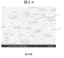
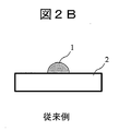
- the flowchart explaining a series of processes from sample production to observation The figure which shows the image which observed the ionic liquid dripped at the silicon substrate hydrophilized by the scanning electron microscope of the acceleration of 1 keV (conventional example). The figure which shows typically the droplet shape of the ionic liquid dripped at the silicon substrate hydrophilized (conventional example). The figure which shows the image (60 degree inclination) which observed the particulate sample (toner) mounted in the ionic liquid of FIG. 1 with the scanning electron microscope of the acceleration of 1-keV. The figure which shows the image which observed the particulate sample (toner) mounted in the ionic liquid of FIG. 1 with the scanning electron microscope of the acceleration of 0.5 keV (conventional example).
- the figure explaining schematic structure of a plasma irradiation apparatus The figure which shows the image which observed the ionic liquid formed into the film form on the silicon substrate by plasma irradiation with the scanning electron microscope of the acceleration of 1 keV.
- Example 1 [Ionic liquid] The inventor has confirmed by experiments that the droplet shape is collapsed by irradiating the droplet of the ionic liquid (PhCH2N + Me2Et [(CF3SO2) 2N] ⁇ ) with plasma and spreads in a film shape on the substrate. The inventor has the same effect on other ionic liquids (Et 3 N + (CH 2 ) 5 CH 3 [(CF 3 SO 2 ) 2 N] ⁇ ) and (C 7 H 19 NO 4 S). Also confirmed. In this embodiment, any one of these ionic liquids is used. The contents of the following examples can be applied to both a hydrophilic ionic liquid and a hydrophobic ionic liquid.
- a hydrophilic treatment is performed on the conductive substrate.
- a known method is used for the hydrophilic treatment.
- the substrate can be hydrophilized by plasma irradiation.
- the substrate preferably has conductivity in consideration of observation with an electron microscope.
- the material of the substrate is arbitrary as long as it is flat to some extent. For example, a silicon substrate, a glass substrate, an aluminum substrate, or a resin substrate may be used.
- an ionic liquid can be changed to a film
- Step 102 A solution in which the ionic liquid is diluted is dropped on the substrate.
- the ionic liquid for example, water or ethanol is used.
- the concentration of the ionic liquid is not limited to this value and may be any percentage.
- a solution diluted to 1% may be used, or an ionic liquid having a concentration of 100% (not diluted) may be used.
- Step 103 excess ionic liquid is removed.
- a filter paper is placed on the substrate surface, and excess ionic liquid is adsorbed on the filter paper side.
- a blower or a micropipette may be used to remove the excess of the ionic liquid. Note that the step of removing the excess of the ionic liquid is not essential.
- Step 104 the substrate after the processing up to the previous step is placed in a plasma irradiation apparatus, and the ionic liquid is irradiated with plasma.
- the plasma generation conditions will be described later. Due to the plasma irradiation, the ionic liquid droplets changed into a film. The optimum film thickness varies depending on the sample to be observed. In general, the longer the plasma irradiation time or the stronger the irradiation intensity (the higher the irradiation energy), the thinner the film thickness. In any case, the ionic liquid after film formation only needs to have a sufficient thickness for adhesion of the sample.
- Step 105 A sample is placed on the surface of the ionic liquid changed into a film shape.
- a particulate sample is placed, but a powder sample may be used.
- the sample may be a porous material, an insulator, a conductive material, or a material that is generally difficult to fix.
- the production of the specimen is completed up to this step.
- Step 106 The specimen is placed in a scanning electron microscope (SEM) and the sample surface is observed. In this example, observation is made at an acceleration voltage of 5 keV or less. However, 5 keV is an example, and is not intended to exclude acceleration voltages exceeding 5 keV.
- 2A and 2B show a state immediately after the ionic liquid solution (2% ethanol solution) is dropped onto the silicon substrate 2 whose substrate surface has been made hydrophilic.
- the ionic liquid 1 dropped on the silicon substrate 2 is in the form of droplets due to its high surface tension.
- the height of the droplet is about the same as the size of the contact surface.
- FIG. 3 and FIG. 4 show an electron microscope image when the particulate sample (toner) 3 is mounted on the surface of such an ionic liquid 1 and observed.
- the particulate sample (toner) 3 is buried in the ionic liquid 1.
- the film 4 of the ionic liquid 1 covers the surface structure of the particulate sample (toner) 3.
- FIG. 5 shows a schematic diagram of the plasma irradiation apparatus used in step 104.
- oxygen plasma is generated by the discharge electrode 6 disposed in the decompression vessel 5 and is irradiated to the ionic liquid 1 dropped on the silicon substrate 2.
- the silicon substrate 2 is placed on a sample stage 8. Further, the inside of the decompression vessel 5 is decompressed to an atmospheric pressure or less by an exhaust pump 9.
- the plasma generation conditions such as the pressure in the decompression vessel 5 and the type of plasma are not particularly limited.
- plasma may be generated and irradiated to the ionic liquid 1 in an argon gas atmosphere, or plasma may be generated and irradiated to the ionic liquid 1 in a mixed atmosphere of argon gas and oxygen gas.
- the atmospheric pressure may be atmospheric pressure as long as plasma is generated.
- the ionic liquid 1 is irradiated with plasma having a discharge current of 7 mA for 30 seconds.
- This numerical value is an example, and if the discharge current is small, the irradiation time may be lengthened. If the discharge current is large (for example, 10 mA), the irradiation time may be shortened.
- the plasma may be generated with an intensity of about 10W. In any case, the generation conditions may be determined so that the ionic liquid 1 is formed into a thickness suitable for adhesion of the particulate sample (toner) 3.
- FIGS. 6A and 6B show the state of the ionic liquid 1 after plasma irradiation.
- FIG. 6A is a scanning electron microscope image captured at an acceleration of 1 KkeV. It can be seen that the scanning electron microscope image of FIG. 6A is flattened with no gradation change observed in the ionic liquid 1 as compared to the scanning electron microscope image of FIG. 2A taken under the same conditions. This is because the ionic liquid 1 spreads along the surface of the silicon substrate 1 by the plasma irradiation as shown in FIG. 6B.
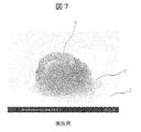
- FIG. 7 and 8 show an electron microscope image when the particulate sample (toner) 3 is mounted and observed on the surface of the ionic liquid 1 formed into a film by plasma irradiation.
- the particulate sample 3 is bonded to the silicon substrate 2 with the ionic liquid 1 only on the lower surface thereof.
- the particulate sample (toner 3) can be observed in a state where the entire surface is exposed (without the surface structure of the sample being buried in the ionic liquid 1).
- FIG. 9 shows a schematic diagram of a scanning electron microscope used in step 106.
- the electron beam 11 taken out from the electron gun 10 is accelerated at 5 keV or less, and then converged by the condenser lens 12 and the objective lens 13 and fixed on the surface of the silicon substrate 2 through the ionic liquid 1 ( The surface of the toner 3 is irradiated and the generated signal is detected by the secondary electron detector 15.
- secondary electrons are detected and a secondary electron image is observed, but a reflected electron image may be observed. It can also be used for EDX (Energy dispersive X-ray spectrometry) analysis in which characteristic X-rays are detected and spectrally separated by energy.
- EDX Electronicgy dispersive X-ray spectrometry
- the ionic liquid 1 dropped on the silicon substrate 2 is irradiated with plasma to form a thin film, and then the particulate sample (toner) 3 is placed on the observation surface of the particulate sample 3.
- the particulate sample 3 is not buried in the ionic liquid 1 or its surface structure is not covered with the ionic liquid 1. Therefore, it is particularly suitable for observing the original surface structure of the sample with a low acceleration voltage SEM.
- a conductive adhesive such as a carbon paste
- the particulate sample 3 is carbon-based
- the carbon paste may interfere with observation.
- the ionic liquid 1 is used as a fixing material as in the present embodiment, there are no restrictions as in the conventional method, so that variations of samples to be observed can be further increased.
- the thin ionic liquid 1 as in this embodiment is used as a fixing material, it is possible to easily fix a sample having a size that is difficult to fix with a conventional conductive adhesive such as carbon paste.
- conductive adhesives such as carbon paste are dry at the time of observation, and often only the conductive filler remains.
- the particulate sample 3 and the conductive filler are in contact with each other at a plurality of points.
- the ionic liquid 1 is in a liquid state even in a vacuum. For this reason, the contact between the ionic liquid 1 and the particulate sample 3 is a surface contact, and the charge-up suppressing effect during observation is higher than that of the conventional method.
- Example 2 Here, a modification to the first embodiment will be described.
- plasma was irradiated to form the ionic liquid 1 into a film (flattening), but the same effect can be obtained by irradiating the droplets of the ionic liquid 1 applied on the silicon substrate 2 with ultraviolet rays.
- the inventor confirmed that.
- the ionic liquid 1 was formed into a film (flattened) by irradiating the ionic liquid 1 with ultraviolet rays including wavelengths of 185 nm and 254 nm for 5 minutes.
- FIG. 10 shows a state after the ionic liquid solution is applied to the silicon substrate 2 and then irradiated with ultraviolet rays. Also in FIG. 10, it can be seen that the ionic liquid 1 spreads in a film shape.
- the wavelength of ultraviolet rays there is no particular limitation on the wavelength of ultraviolet rays as long as the inventors know.
- ultraviolet rays including a plurality of wavelengths are used.
- the ionic liquid 1 may be irradiated with ultraviolet rays having a wavelength of only 185 nm or only having a wavelength of 254 nm.
- the ultraviolet irradiation time is set to 5 minutes. However, this time is an example, and it may be 3 minutes or 7 minutes.
- the longer the irradiation time of ultraviolet rays the greater the energy applied
- the thinner the film thickness In any case, it suffices to have a thickness sufficient for bonding the sample.
- the particulate sample 3 is not buried in the ionic liquid 1 or its surface structure is not covered with the ionic liquid 1, so The surface structure of can be easily observed.
- the present invention is not limited to the above-described embodiments, and includes various modifications.
- Ar ion beam or Ga ion beam may be irradiated to the ionic liquid 1 at an acceleration of about 1.2 kV to form the ionic liquid 1 into a film (flattened).
- the hydrophilic treatment is performed before the ionic liquid 1 is dropped or applied on the surface of the silicon substrate 2.
- the surface of the substrate on which the ionic liquid 1 is dropped or applied may be hydrophobic.
- the above-described embodiment is an aspect of the present invention, and it is not necessary to include all the components of each embodiment.
- a part of the configuration of a certain embodiment can be replaced with the configuration of another embodiment, and the configuration of another embodiment can be added to the configuration of a certain embodiment.
Landscapes
- Chemical & Material Sciences (AREA)
- Analytical Chemistry (AREA)
- Analysing Materials By The Use Of Radiation (AREA)
- Sampling And Sample Adjustment (AREA)
Abstract
液滴状に付着したイオン液体に、プラズマ、紫外線又はイオンビームを照射することで液滴形状を膜状に変形させた後、観察対象とする試料を膜状に変化したイオン液体に載置する。
Description
本発明は、基板に固定された試料を電子顕微鏡を用いて観察する方法に関する。また、本発明は、前記観察のための標本を生産する方法に関する。
従来、走査型電子顕微鏡を用いて、粉体又は粒子状試料の表面を観察する場合、導電性接着剤や導電テープを用いて試料を基板に固定する手法が用いられている。導電性接着剤は、溶媒の揮発により固化し、試料を基板に固定する。一方で、導電性接着剤は、粉体又は粒子状試料の固定に用いる場合、最適なタイミングで試料を基板に搭載する必要がある。例えば搭載のタイミングが早すぎると、試料が導電性接着剤に埋没してしまう。一方、搭載のタイミングが遅いと、導電性接着剤が乾燥してしまい、試料を基板に接着できなくなる。なお、導電テープには乾燥の心配はないが、その粘着層に厚みがあるため、試料の安定性に欠ける。このため、導電テープは、試料の高倍率観察には適していない。
そこで、イオン液体を用いて試料を基板に接着する手法が検討されている(特許文献1)。イオン液体とは常温で液体の塩であり、蒸気圧がほぼゼロの液体である。また、イオン液体は、イオン導電性を有するため、導電基板との接着にも適している。
しかし、イオン液体は表面張力が高いため、接着剤として利用するために基板に塗布すると、イオン液体は厚みのある液滴になってしまう。液滴状のイオン液体に粒子状試料を搭載すると、前述した導電性接着剤と同様、試料が液滴中に埋没し、又は、試料表面の微細構造がイオン液体に覆い隠されてしまい、試料本来の表面構造の観察が困難である。
本発明は、上記課題を解決するために、特許請求の範囲に記載の構成を採用する。すなわち、本発明は、試料を搭載する前のイオン液体の液滴に、プラズマ、紫外線又はイオンビームを照射することにより液滴の形状を膜状に変形させる手法を採用する。
本発明によれば、試料を基板に固定する際に、試料がイオン液体中に埋没し、又は、試料表面の微細構造がイオン液体に覆い隠されないようにできる。前述した以外の課題、構成及び効果は、以下の実施の形態の説明により明らかにされる。
以下、図面に基づいて、本発明の実施の形態を説明する。なお、本発明の実施の態様は、後述する形態例に限定されるものではなく、その技術思想の範囲において、種々の変形が可能である。
[実施例1]
[イオン液体]
発明者は、イオン液体(PhCH2N+Me2Et[(CF3SO2)2N]-)の液滴にプラズマを照射することで液滴の形状が崩れ、基板上に膜状に広がる現象を実験により確認した。また、発明者は、同様の効果を、他のイオン液体(Et3N+(CH2)5CH3[(CF3SO2)2N]-)及び(C7H19NO4S)についても確認した。本実施例では、これらイオン液体のいずれかを使用する。なお以降の実施例の内容は親水性のイオン液体、疎水性のイオン液体双方に適用することが可能である。
[イオン液体]
発明者は、イオン液体(PhCH2N+Me2Et[(CF3SO2)2N]-)の液滴にプラズマを照射することで液滴の形状が崩れ、基板上に膜状に広がる現象を実験により確認した。また、発明者は、同様の効果を、他のイオン液体(Et3N+(CH2)5CH3[(CF3SO2)2N]-)及び(C7H19NO4S)についても確認した。本実施例では、これらイオン液体のいずれかを使用する。なお以降の実施例の内容は親水性のイオン液体、疎水性のイオン液体双方に適用することが可能である。
[観察手順]
図1を用いて、今回開発した観察手順を説明する。
・ステップ101
導電性を有する基板に対して親水化処理を実行する。親水化処理には、既知の手法を使用する。例えばプラズマの照射により、基板を親水化することができる。基板は、電子顕微鏡による観察を考慮すると導電性を有することが好ましい。基板は、ある程度平坦な物であれば材質は任意である。例えばシリコン基板、ガラス基板、アルミニウム基板、樹脂基板でもよい。なお、基板を親水化しなくても、後述する処理により、イオン液体を膜状に変化させることができる。もっとも、基板を親水化しておくことにより、後述する処理によるイオン液体の膜化が一段と容易になる。
図1を用いて、今回開発した観察手順を説明する。
・ステップ101
導電性を有する基板に対して親水化処理を実行する。親水化処理には、既知の手法を使用する。例えばプラズマの照射により、基板を親水化することができる。基板は、電子顕微鏡による観察を考慮すると導電性を有することが好ましい。基板は、ある程度平坦な物であれば材質は任意である。例えばシリコン基板、ガラス基板、アルミニウム基板、樹脂基板でもよい。なお、基板を親水化しなくても、後述する処理により、イオン液体を膜状に変化させることができる。もっとも、基板を親水化しておくことにより、後述する処理によるイオン液体の膜化が一段と容易になる。
・ステップ102
イオン液体を希釈した溶液を基板上に滴下する。イオン液体の希釈化には、例えば水やエタノールを使用する。本実施例では、イオン液体の濃度を2%に希釈した溶液を使用した。もっとも、イオン液体の濃度はこの数値に限らず、何%でもよい。例えば1%に希釈した溶液でもよいし、100%濃度の(希釈していない)イオン液体を用いもよい。
イオン液体を希釈した溶液を基板上に滴下する。イオン液体の希釈化には、例えば水やエタノールを使用する。本実施例では、イオン液体の濃度を2%に希釈した溶液を使用した。もっとも、イオン液体の濃度はこの数値に限らず、何%でもよい。例えば1%に希釈した溶液でもよいし、100%濃度の(希釈していない)イオン液体を用いもよい。
・ステップ103
乾燥を早めるため、イオン液体の余剰分を除去する。例えば濾紙を基板表面に被せ、余剰なイオン液体を濾紙側に吸着させる。もっとも、イオン液体の余剰分の除去には、ブロワーを用いてもよいし、マイクロピペットを用いてもよい。なお、イオン液体の余剰分を除去するステップは必須ではない。
乾燥を早めるため、イオン液体の余剰分を除去する。例えば濾紙を基板表面に被せ、余剰なイオン液体を濾紙側に吸着させる。もっとも、イオン液体の余剰分の除去には、ブロワーを用いてもよいし、マイクロピペットを用いてもよい。なお、イオン液体の余剰分を除去するステップは必須ではない。
・ステップ104
本実施例では、前ステップまでの処理が終了した基板をプラズマ照射装置内に配置し、イオン液体にプラズマを照射する。プラズマの発生条件については後述する。プラズマの照射により、イオン液体の液滴は膜状に変化した。最適な膜の厚みは、観察対象とする試料に応じて異なる。一般に、プラズマの照射時間が長いほど又は照射強度が強いほど(照射されるエネルギーが大きいほど)、膜厚は薄くなる。いずれにしても、膜化後のイオン液体は、試料の接着に十分な厚みを有していればよい。
本実施例では、前ステップまでの処理が終了した基板をプラズマ照射装置内に配置し、イオン液体にプラズマを照射する。プラズマの発生条件については後述する。プラズマの照射により、イオン液体の液滴は膜状に変化した。最適な膜の厚みは、観察対象とする試料に応じて異なる。一般に、プラズマの照射時間が長いほど又は照射強度が強いほど(照射されるエネルギーが大きいほど)、膜厚は薄くなる。いずれにしても、膜化後のイオン液体は、試料の接着に十分な厚みを有していればよい。
・ステップ105
膜状に変化したイオン液体の表面に試料を載置する。本実施例では粒子状試料を載置しているが、紛体試料でもよい。なお、試料は、多孔質材料、絶縁物、導電性材料、一般に固定の難しい材料であってもよい。このステップまでで標本の生産が終了する。
膜状に変化したイオン液体の表面に試料を載置する。本実施例では粒子状試料を載置しているが、紛体試料でもよい。なお、試料は、多孔質材料、絶縁物、導電性材料、一般に固定の難しい材料であってもよい。このステップまでで標本の生産が終了する。
・ステップ106
標本を走査型電子顕微鏡(SEM: Scanning Electron Microscope)内に配置して試料表面を観察する。本実施例では、5keV以下の加速電圧で観察する。もっとも、5keVは一例であり、5keVを超える加速電圧を排除する趣旨ではない。
標本を走査型電子顕微鏡(SEM: Scanning Electron Microscope)内に配置して試料表面を観察する。本実施例では、5keV以下の加速電圧で観察する。もっとも、5keVは一例であり、5keVを超える加速電圧を排除する趣旨ではない。
[従来手法によるイオン液体を用いた観察]
図2A及び図2Bに、基板表面を親水化したシリコン基板2にイオン液体溶液(2%エタノール溶液)を滴下した直後の状態を示す。
図2A及び図2Bに、基板表面を親水化したシリコン基板2にイオン液体溶液(2%エタノール溶液)を滴下した直後の状態を示す。
図2A及び図2Bに示すように、シリコン基板2上に滴下されたイオン液体1は、その表面張力の高さから液滴状となっている。図2Bでは、液滴の高さが接触面の寸法と同程度になっている。図3及び図4に、このようなイオン液体1の表面に粒子状試料(トナー)3を搭載して観察した場合の電子顕微鏡像を示す。図3では、粒子状試料(トナー)3がイオン液体1中に埋没してしまっている。図4では、イオン液体1の膜4が粒子状試料(トナー)3の表面構造を覆い隠してしまっている。
[実施例の手法によるイオン液体を用いた観察]
図5に、ステップ104で使用するプラズマ照射装置の模式図を示す。本実施例では、減圧容器5内に配置された放電電極6で酸素プラズマを発生し、シリコン基板2に滴下されたイオン液体1に照射する。図中、シリコン基板2は試料ステージ8に載置されている。また、減圧容器5内は、排気ポンプ9によって大気圧以下に減圧されている。
図5に、ステップ104で使用するプラズマ照射装置の模式図を示す。本実施例では、減圧容器5内に配置された放電電極6で酸素プラズマを発生し、シリコン基板2に滴下されたイオン液体1に照射する。図中、シリコン基板2は試料ステージ8に載置されている。また、減圧容器5内は、排気ポンプ9によって大気圧以下に減圧されている。
減圧容器5内の気圧、プラズマの種類などのプラズマ発生条件は特に限定しない。例えばアルゴンガス雰囲気中でプラズマを発生してイオン液体1に照射しても構わないし、アルゴンガスと酸素ガスの混合雰囲気中でプラズマを発生してイオン液体1に照射しても構わない。気圧はプラズマが発生しさえすれば大気圧でもよい。
本実施例では、イオン液体1に対して、放電電流7mAのプラズマを30sec照射する。なお、この数値は一例であり、放電電流が小さければ照射時間を長くすればよい。また、放電電流が大きければ(例えば10mA)、照射時間を短くすればよい。また、プラズマは10W程度の強度で発生しても良い。いずれにしても、イオン液体1が、粒子状試料(トナー)3の接着に適した厚みに膜化するように発生条件を決定すればよい。
図6A及び図6Bに、プラズマ照射後のイオン液体1の様子を示す。図6Aは、1 keVの加速度で撮像した走査電子顕微鏡像である。図6Aの走査電子顕微鏡像は、同じ条件で撮像した図2Aの走査電子顕微鏡像に比して、イオン液体1に階調変化が認められず、平坦化していることが分かる。これは、図6Bに示すように、プラズマの照射により、イオン液体1がシリコン基板1の表面に沿って広がったためである。
図7及び図8に、プラズマ照射によって膜化したイオン液体1の表面に粒子状試料(トナー)3を搭載して観察した場合の電子顕微鏡像を示す。図7示すように、粒子状試料3は、その下面でのみイオン液体1によりシリコン基板2に接着されている。このため、図8に示すように、粒子状試料(トナー3)は、表面全体が露出した状態で(試料の表面構造がイオン液体1に埋没することなく)観察することができる。
[走査型電子顕微鏡の構成]
図9に、ステップ106で使用する走査型電子顕微鏡の模式図を示す。本実施例では、電子銃10から取り出した電子ビーム11を5keV以下で加速した後、コンデンサーレンズ12および対物レンズ13により収束し、シリコン基板2の表面上にイオン液体1を通じて固定した粒子状試料(トナー)3の表面に照射し、発生した信号を二次電子検出器15で検出する。本実施例では、二次電子を検出して二次電子像を観察しているが、反射電子像を観察してもよい。また、特性X線を検出してエネルギーで分光する、EDX(Energy dispersive X-ray spectrometry)分析にも用いることができる。
図9に、ステップ106で使用する走査型電子顕微鏡の模式図を示す。本実施例では、電子銃10から取り出した電子ビーム11を5keV以下で加速した後、コンデンサーレンズ12および対物レンズ13により収束し、シリコン基板2の表面上にイオン液体1を通じて固定した粒子状試料(トナー)3の表面に照射し、発生した信号を二次電子検出器15で検出する。本実施例では、二次電子を検出して二次電子像を観察しているが、反射電子像を観察してもよい。また、特性X線を検出してエネルギーで分光する、EDX(Energy dispersive X-ray spectrometry)分析にも用いることができる。
[まとめ]
本実施例で説明したように、シリコン基板2に滴下されたイオン液体1にプラズマを照射して薄膜化した後に粒子状試料(トナー)3を載置することにより、粒子状試料3の観察面の全体を露出した状態でシリコン基板2に固定することができる。すなわち、粒子状試料3がイオン液体1に埋没することがない、又は、その表面構造がイオン液体1で覆い隠されることがない。従って、特に低加速電圧SEMによる試料本来の表面構造の観察に適している。
本実施例で説明したように、シリコン基板2に滴下されたイオン液体1にプラズマを照射して薄膜化した後に粒子状試料(トナー)3を載置することにより、粒子状試料3の観察面の全体を露出した状態でシリコン基板2に固定することができる。すなわち、粒子状試料3がイオン液体1に埋没することがない、又は、その表面構造がイオン液体1で覆い隠されることがない。従って、特に低加速電圧SEMによる試料本来の表面構造の観察に適している。
従来手法のように、粒子状試料3の固定にカーボンペーストなどの導電性接着剤を用いる場合に、粒子状試料3がカーボン系であると、カーボンペーストが観察を妨げることもある。しかし、本実施例のように、イオン液体1を固定材として利用すれば、従来手法のような制約がないため、観察対象とする試料のバリエーションを一段と増やすことができる。
また、本実施例のように薄膜化したイオン液体1を固定材に用いれば、従来用いられているカーボンペーストなどの導電接着剤では固定が難しい寸法の試料も容易に固定することができる。
また、カーボンペーストなどの導電性接着剤は観察時には乾燥しており、導電性フィラーのみが残っている状態になることが多い。しかし、この状態では、粒子状試料3と導電性フィラーは複数の点で接触している形となる。しかし、本実施例のように、イオン液体1は真空中でも液体状である。このため、イオン液体1と粒子状試料3との接触は面接触となり、観察中のチャージアップ抑制効果も従来手法に比して高くなる。
[実施例2]
ここでは、実施例1に対する変形例を説明する。実施例1では、プラズマを照射してイオン液体1を膜化(平坦化)したが、シリコン基板2上に塗布したイオン液体1の液滴に紫外線を照射することによっても同様の効果が得られることを発明者は確認した。本実施例では、185nmの波長と254nmの波長を含む紫外線を、5min間、イオン液体1に照射してイオン液体1の膜化(平坦化)を実現した。図10に、シリコン基板2にイオン液体溶液を塗布した後に、紫外線を照射した後の状態を示す。図10でも、イオン液体1は膜状に広がっていることが分かる。
ここでは、実施例1に対する変形例を説明する。実施例1では、プラズマを照射してイオン液体1を膜化(平坦化)したが、シリコン基板2上に塗布したイオン液体1の液滴に紫外線を照射することによっても同様の効果が得られることを発明者は確認した。本実施例では、185nmの波長と254nmの波長を含む紫外線を、5min間、イオン液体1に照射してイオン液体1の膜化(平坦化)を実現した。図10に、シリコン基板2にイオン液体溶液を塗布した後に、紫外線を照射した後の状態を示す。図10でも、イオン液体1は膜状に広がっていることが分かる。
なお、発明者の知見による限り、紫外線の波長について特に制限はない。また、本実施例では複数の波長を含む紫外線を用いているが、185nmの波長のみ、又は、254nmの波長のみの紫外線をイオン液体1に照射してもよい。勿論、他の波長を含む紫外線をイオン液体1に照射してもよい。また、本実施例では、紫外線の照射時間を5minとしているが、この時間は一例であり、3minでも、7minでも構わない。プラズマ照射の場合と同様、紫外線の照射時間が長くほど(照射されるエネルギーが大きいほど)、膜厚は薄くなる。いずれにしても、試料の接着に十分な厚みを有していればよい。
[まとめ]
本実施例の場合も、実施例1の場合と同様、粒子状試料3がイオン液体1に埋没することがない、又は、その表面構造がイオン液体1で覆い隠されることがないため、試料本来の表面構造を容易に観察することができる。
本実施例の場合も、実施例1の場合と同様、粒子状試料3がイオン液体1に埋没することがない、又は、その表面構造がイオン液体1で覆い隠されることがないため、試料本来の表面構造を容易に観察することができる。
[他の実施例]
本発明は、前述した実施例に限定されるものではなく、様々な変形例が含まれる。例えばプラズマや紫外線の代わりに、Arイオンビーム又はGaイオンビームを、約1.2kVの加速度でイオン液体1に照射し、イオン液体1を膜化(平坦化)してもよい。また、前述の実施例では、イオン液体1をシリコン基板2の表面に滴下又は塗布する前に親水化処理を施しているが、イオン液体1を滴下又は塗布する基板の表面は疎水性もでも良い。また、上述した実施例は本発明の一態様であり、各実施例の全ての構成要素を備える必要はない。また、ある実施例の構成の一部を他の実施例の構成に置き換えることも可能であり、また、ある実施例の構成に他の実施例の構成を加えることも可能である。また、各実施例の構成の一部について、他の構成の追加、削除又は置換をすることが可能である。
本発明は、前述した実施例に限定されるものではなく、様々な変形例が含まれる。例えばプラズマや紫外線の代わりに、Arイオンビーム又はGaイオンビームを、約1.2kVの加速度でイオン液体1に照射し、イオン液体1を膜化(平坦化)してもよい。また、前述の実施例では、イオン液体1をシリコン基板2の表面に滴下又は塗布する前に親水化処理を施しているが、イオン液体1を滴下又は塗布する基板の表面は疎水性もでも良い。また、上述した実施例は本発明の一態様であり、各実施例の全ての構成要素を備える必要はない。また、ある実施例の構成の一部を他の実施例の構成に置き換えることも可能であり、また、ある実施例の構成に他の実施例の構成を加えることも可能である。また、各実施例の構成の一部について、他の構成の追加、削除又は置換をすることが可能である。
1 イオン液体
2 シリコン基板
3 粒子状試料
4 試料表面を覆うイオン液体の膜
5 減圧容器
6 放電電極
8 試料ステージ
9 排気ポンプ
10 電子銃
11 電子ビーム
12 コンデンサーレンズ
13 対物レンズ
15 二次電子検出器
2 シリコン基板
3 粒子状試料
4 試料表面を覆うイオン液体の膜
5 減圧容器
6 放電電極
8 試料ステージ
9 排気ポンプ
10 電子銃
11 電子ビーム
12 コンデンサーレンズ
13 対物レンズ
15 二次電子検出器
Claims (18)
- イオン液体を含む液滴にエネルギーを供給することで前記液滴を膜状へ変化させる処理を施し、イオン液体膜を作製する処理工程と、
前記イオン液体膜上に試料を搭載し、標本を作製する試料搭載工程と、
前記標本を、走査型電子顕微鏡を使用して観察する観察工程と、を含む観察方法。 - 請求項1に記載の観察方法において、
前記試料は粉状である観察方法。 - 請求項2に記載の観察方法において、
前記観察時の前記走査型電子顕微鏡の加速電圧は5keV以下である、観察方法。 - 請求項3に記載の観察方法において、
前記エネルギーを供給することは前記液滴にプラズマを照射することである、観察方法。 - 請求項4に記載の観察方法において、
導電性を有する基板に対して親水化処理を行い、親水化基板を作製する親水化工程を更に有し、
前記イオン液体膜を制作する前記処理工程は、前記親水化基板に前記液滴を供給することを含む、観察方法。 - 請求項1に記載の観察方法において、
前記観察時の前記走査型電子顕微鏡の加速電圧は5keV以下である、観察方法。 - 請求項1に記載の観察方法において、
前記エネルギーを供給することは前記液滴にプラズマを照射することである、観察方法。 - 請求項1に記載の観察方法において、
導電性を有する基板に対して親水化処理を行い、親水化基板を作製する親水化工程を更に有し、
前記イオン液体膜を制作する前記処理工程は、前記親水化基板に前記液滴を供給することを含む、観察方法。 - 請求項1に記載の観察方法において、
前記エネルギーを供給することは前記液滴に紫外線を照射することである、観察方法。 - 請求項1に記載の観察方法において、
前記エネルギーを供給することは前記液滴にイオンビームを照射することである、観察方法。 - イオン液体を含む液滴にエネルギーを供給することで前記液滴を膜状へ変化させる処理を施し、イオン液体膜を作製する処理工程と、
前記イオン液体膜上に試料を搭載し、標本を作製する試料搭載工程と、を含む標本を生産する方法。 - 請求項11に記載の方法において、
前記試料は粉状である、標本を生産する方法。 - 請求項12に記載の方法において、
前記エネルギーを供給することは前記液滴にプラズマを照射することである、標本を生産する方法。 - 請求項13に記載の方法において、
導電性を有する基板に対して親水化処理を行い、親水化基板を作製する親水化工程を更に有し、
前記イオン液体膜を制作する前記処理工程は、前記親水化基板に前記液滴を供給することを含む、標本を生産する方法。 - 請求項11に記載の方法において、
前記エネルギーを供給することは前記液滴にプラズマを照射することである、標本を生産する方法。 - 請求項11に記載の方法において、
導電性を有する基板に対して親水化処理を行い、親水化基板を作製する親水化工程を更に有し、
前記イオン液体膜を制作する前記処理工程は、前記親水化基板に前記液滴を供給することを含む、標本を生産する方法。 - 請求項11に記載の方法において、
前記エネルギーを供給することは前記液滴に紫外線を照射することである、標本を生産する方法。 - 請求項11に記載の方法において、
前記エネルギーを供給することは前記液滴にイオンビームを照射することである、標本を生産する方法。
Priority Applications (2)
| Application Number | Priority Date | Filing Date | Title |
|---|---|---|---|
| JP2017513921A JP6357583B2 (ja) | 2015-04-24 | 2015-04-24 | イオン液体を用いた試料の観察方法及び標本の生産方法 |
| PCT/JP2015/062461 WO2016170663A1 (ja) | 2015-04-24 | 2015-04-24 | イオン液体を用いた試料の観察方法及び標本の生産方法 |
Applications Claiming Priority (1)
| Application Number | Priority Date | Filing Date | Title |
|---|---|---|---|
| PCT/JP2015/062461 WO2016170663A1 (ja) | 2015-04-24 | 2015-04-24 | イオン液体を用いた試料の観察方法及び標本の生産方法 |
Publications (1)
| Publication Number | Publication Date |
|---|---|
| WO2016170663A1 true WO2016170663A1 (ja) | 2016-10-27 |
Family
ID=57142993
Family Applications (1)
| Application Number | Title | Priority Date | Filing Date |
|---|---|---|---|
| PCT/JP2015/062461 Ceased WO2016170663A1 (ja) | 2015-04-24 | 2015-04-24 | イオン液体を用いた試料の観察方法及び標本の生産方法 |
Country Status (2)
| Country | Link |
|---|---|
| JP (1) | JP6357583B2 (ja) |
| WO (1) | WO2016170663A1 (ja) |
Cited By (1)
| Publication number | Priority date | Publication date | Assignee | Title |
|---|---|---|---|---|
| WO2021176921A1 (ja) * | 2020-03-03 | 2021-09-10 | 日清紡ホールディングス株式会社 | イオン液体を用いた平滑材料の固定方法 |
Citations (5)
| Publication number | Priority date | Publication date | Assignee | Title |
|---|---|---|---|---|
| WO2011074178A1 (ja) * | 2009-12-14 | 2011-06-23 | 株式会社日立ハイテクノロジーズ | 荷電粒子線装置及び試料観察方法 |
| JP2011158257A (ja) * | 2010-01-29 | 2011-08-18 | Hitachi High-Technologies Corp | 像分解能評価用試料,荷電粒子線装置、および試料作成方法 |
| JP2012083146A (ja) * | 2010-10-08 | 2012-04-26 | Hitachi High-Technologies Corp | 液体の表面を浮遊する試料の走査電子顕微鏡観察方法 |
| JP2013096890A (ja) * | 2011-11-02 | 2013-05-20 | Hitachi High-Technologies Corp | 電子顕微法の観察標体、電子顕微法、電子顕微鏡および観察標体作製装置 |
| JP2013257148A (ja) * | 2012-06-11 | 2013-12-26 | Hitachi High-Technologies Corp | コーティング装置、及びコーティング装置の前処理装置 |
-
2015
- 2015-04-24 WO PCT/JP2015/062461 patent/WO2016170663A1/ja not_active Ceased
- 2015-04-24 JP JP2017513921A patent/JP6357583B2/ja active Active
Patent Citations (5)
| Publication number | Priority date | Publication date | Assignee | Title |
|---|---|---|---|---|
| WO2011074178A1 (ja) * | 2009-12-14 | 2011-06-23 | 株式会社日立ハイテクノロジーズ | 荷電粒子線装置及び試料観察方法 |
| JP2011158257A (ja) * | 2010-01-29 | 2011-08-18 | Hitachi High-Technologies Corp | 像分解能評価用試料,荷電粒子線装置、および試料作成方法 |
| JP2012083146A (ja) * | 2010-10-08 | 2012-04-26 | Hitachi High-Technologies Corp | 液体の表面を浮遊する試料の走査電子顕微鏡観察方法 |
| JP2013096890A (ja) * | 2011-11-02 | 2013-05-20 | Hitachi High-Technologies Corp | 電子顕微法の観察標体、電子顕微法、電子顕微鏡および観察標体作製装置 |
| JP2013257148A (ja) * | 2012-06-11 | 2013-12-26 | Hitachi High-Technologies Corp | コーティング装置、及びコーティング装置の前処理装置 |
Cited By (6)
| Publication number | Priority date | Publication date | Assignee | Title |
|---|---|---|---|---|
| WO2021176921A1 (ja) * | 2020-03-03 | 2021-09-10 | 日清紡ホールディングス株式会社 | イオン液体を用いた平滑材料の固定方法 |
| JP2021137995A (ja) * | 2020-03-03 | 2021-09-16 | 日清紡ホールディングス株式会社 | イオン液体を用いた平滑材料の固定方法 |
| CN115243882A (zh) * | 2020-03-03 | 2022-10-25 | 日清纺控股株式会社 | 使用离子液体的平滑材料的固定方法 |
| CN115243882B (zh) * | 2020-03-03 | 2024-03-01 | 日清纺控股株式会社 | 使用离子液体的平滑材料的固定方法 |
| JP7543659B2 (ja) | 2020-03-03 | 2024-09-03 | 日清紡ホールディングス株式会社 | イオン液体を用いた平滑材料の固定方法 |
| US12202239B2 (en) | 2020-03-03 | 2025-01-21 | Nisshinbo Holdings Inc. | Method for fixing smooth materials using ionic liquid |
Also Published As
| Publication number | Publication date |
|---|---|
| JP6357583B2 (ja) | 2018-07-11 |
| JPWO2016170663A1 (ja) | 2017-12-28 |
Similar Documents
| Publication | Publication Date | Title |
|---|---|---|
| US9947505B2 (en) | Graphene modification | |
| JP5442417B2 (ja) | 荷電粒子線装置及び試料観察方法 | |
| Coffinier et al. | Diamond nanowires for highly sensitive matrix-free mass spectrometry analysis of small molecules | |
| WO2007112234A2 (en) | Means and method for analyzing samples by mass spectrometry | |
| JP7404195B2 (ja) | 試料支持体、イオン化法、及び質量分析方法 | |
| CN111699384B (zh) | 试样支承体 | |
| JP2010071727A (ja) | 質量分析用デバイス及びそれを用いた質量分析装置、質量分析方法 | |
| JP5292326B2 (ja) | 標準試料作成方法、および標準試料 | |
| Silina et al. | The role of physical and chemical properties of Pd nanostructured materials immobilized on inorganic carriers on ion formation in atmospheric pressure laser desorption/ionization mass spectrometry | |
| JP6357583B2 (ja) | イオン液体を用いた試料の観察方法及び標本の生産方法 | |
| US7777404B1 (en) | Field emission type electron gun comprising single fibrous carbon electron emitter and operating method for the same | |
| EP3152582B1 (en) | Methods of detecting biological prints, fluids or analytes therein using porous semiconductor substrates | |
| WO2009001963A1 (ja) | Maldi質量分析用の試料ホルダおよび質量分析方法 | |
| JP5072682B2 (ja) | 質量分析用デバイス、これを用いる質量分析装置および質量分析方法 | |
| JP5149635B2 (ja) | 光電子分光分析方法 | |
| WO2023157392A1 (ja) | 試料支持体、及び試料支持体の製造方法 | |
| Jemere et al. | Matrix‐free laser desorption/ionization mass spectrometry using silicon glancing angle deposition (GLAD) films | |
| JP2021047151A (ja) | レーザー脱離/イオン化質量分析用基板、及び、それを用いたレーザー脱離/イオン化質量分析法 | |
| CN110459454A (zh) | 一种将可调谐深紫外激光源与近常压光发射电子显微镜联合的成像系统及方法 | |
| RU2217840C1 (ru) | Способ формирования шероховатой поверхности кремниевых подложек и электролит для анодного травления кремниевых подложек | |
| JP3207675U (ja) | 基材の表面上を親水性とする作成装置 | |
| JPS63205033A (ja) | 液体金属イオン源の製造方法 | |
| KR20250072863A (ko) | 빔 유도 증착을 위한 탄소 함유 전구체 | |
| JPS63229345A (ja) | 定量分析用標準試料の作成方法 | |
| Cui | The application of ultrafast laser pulses to laser desorption mass spectrometry |
Legal Events
| Date | Code | Title | Description |
|---|---|---|---|
| 121 | Ep: the epo has been informed by wipo that ep was designated in this application |
Ref document number: 15889902 Country of ref document: EP Kind code of ref document: A1 |
|
| ENP | Entry into the national phase |
Ref document number: 2017513921 Country of ref document: JP Kind code of ref document: A |
|
| NENP | Non-entry into the national phase |
Ref country code: DE |
|
| 122 | Ep: pct application non-entry in european phase |
Ref document number: 15889902 Country of ref document: EP Kind code of ref document: A1 |