WO2016167358A1 - 蒸着パターンの形成方法、押さえ板一体型の押し込み部材、蒸着装置及び有機半導体素子の製造方法 - Google Patents
蒸着パターンの形成方法、押さえ板一体型の押し込み部材、蒸着装置及び有機半導体素子の製造方法 Download PDFInfo
- Publication number
- WO2016167358A1 WO2016167358A1 PCT/JP2016/062151 JP2016062151W WO2016167358A1 WO 2016167358 A1 WO2016167358 A1 WO 2016167358A1 JP 2016062151 W JP2016062151 W JP 2016062151W WO 2016167358 A1 WO2016167358 A1 WO 2016167358A1
- Authority
- WO
- WIPO (PCT)
- Prior art keywords
- vapor deposition
- mask
- pattern
- forming
- deposition mask
- Prior art date
- Legal status (The legal status is an assumption and is not a legal conclusion. Google has not performed a legal analysis and makes no representation as to the accuracy of the status listed.)
- Ceased
Links
Images








Classifications
-
- H—ELECTRICITY
- H10—SEMICONDUCTOR DEVICES; ELECTRIC SOLID-STATE DEVICES NOT OTHERWISE PROVIDED FOR
- H10K—ORGANIC ELECTRIC SOLID-STATE DEVICES
- H10K71/00—Manufacture or treatment specially adapted for the organic devices covered by this subclass
- H10K71/10—Deposition of organic active material
- H10K71/16—Deposition of organic active material using physical vapour deposition [PVD], e.g. vacuum deposition or sputtering
- H10K71/166—Deposition of organic active material using physical vapour deposition [PVD], e.g. vacuum deposition or sputtering using selective deposition, e.g. using a mask
-
- C—CHEMISTRY; METALLURGY
- C23—COATING METALLIC MATERIAL; COATING MATERIAL WITH METALLIC MATERIAL; CHEMICAL SURFACE TREATMENT; DIFFUSION TREATMENT OF METALLIC MATERIAL; COATING BY VACUUM EVAPORATION, BY SPUTTERING, BY ION IMPLANTATION OR BY CHEMICAL VAPOUR DEPOSITION, IN GENERAL; INHIBITING CORROSION OF METALLIC MATERIAL OR INCRUSTATION IN GENERAL
- C23C—COATING METALLIC MATERIAL; COATING MATERIAL WITH METALLIC MATERIAL; SURFACE TREATMENT OF METALLIC MATERIAL BY DIFFUSION INTO THE SURFACE, BY CHEMICAL CONVERSION OR SUBSTITUTION; COATING BY VACUUM EVAPORATION, BY SPUTTERING, BY ION IMPLANTATION OR BY CHEMICAL VAPOUR DEPOSITION, IN GENERAL
- C23C14/00—Coating by vacuum evaporation, by sputtering or by ion implantation of the coating forming material
- C23C14/04—Coating on selected surface areas, e.g. using masks
- C23C14/042—Coating on selected surface areas, e.g. using masks using masks
-
- C—CHEMISTRY; METALLURGY
- C23—COATING METALLIC MATERIAL; COATING MATERIAL WITH METALLIC MATERIAL; CHEMICAL SURFACE TREATMENT; DIFFUSION TREATMENT OF METALLIC MATERIAL; COATING BY VACUUM EVAPORATION, BY SPUTTERING, BY ION IMPLANTATION OR BY CHEMICAL VAPOUR DEPOSITION, IN GENERAL; INHIBITING CORROSION OF METALLIC MATERIAL OR INCRUSTATION IN GENERAL
- C23C—COATING METALLIC MATERIAL; COATING MATERIAL WITH METALLIC MATERIAL; SURFACE TREATMENT OF METALLIC MATERIAL BY DIFFUSION INTO THE SURFACE, BY CHEMICAL CONVERSION OR SUBSTITUTION; COATING BY VACUUM EVAPORATION, BY SPUTTERING, BY ION IMPLANTATION OR BY CHEMICAL VAPOUR DEPOSITION, IN GENERAL
- C23C14/00—Coating by vacuum evaporation, by sputtering or by ion implantation of the coating forming material
- C23C14/04—Coating on selected surface areas, e.g. using masks
-
- C—CHEMISTRY; METALLURGY
- C23—COATING METALLIC MATERIAL; COATING MATERIAL WITH METALLIC MATERIAL; CHEMICAL SURFACE TREATMENT; DIFFUSION TREATMENT OF METALLIC MATERIAL; COATING BY VACUUM EVAPORATION, BY SPUTTERING, BY ION IMPLANTATION OR BY CHEMICAL VAPOUR DEPOSITION, IN GENERAL; INHIBITING CORROSION OF METALLIC MATERIAL OR INCRUSTATION IN GENERAL
- C23C—COATING METALLIC MATERIAL; COATING MATERIAL WITH METALLIC MATERIAL; SURFACE TREATMENT OF METALLIC MATERIAL BY DIFFUSION INTO THE SURFACE, BY CHEMICAL CONVERSION OR SUBSTITUTION; COATING BY VACUUM EVAPORATION, BY SPUTTERING, BY ION IMPLANTATION OR BY CHEMICAL VAPOUR DEPOSITION, IN GENERAL
- C23C14/00—Coating by vacuum evaporation, by sputtering or by ion implantation of the coating forming material
- C23C14/22—Coating by vacuum evaporation, by sputtering or by ion implantation of the coating forming material characterised by the process of coating
- C23C14/24—Vacuum evaporation
-
- C—CHEMISTRY; METALLURGY
- C23—COATING METALLIC MATERIAL; COATING MATERIAL WITH METALLIC MATERIAL; CHEMICAL SURFACE TREATMENT; DIFFUSION TREATMENT OF METALLIC MATERIAL; COATING BY VACUUM EVAPORATION, BY SPUTTERING, BY ION IMPLANTATION OR BY CHEMICAL VAPOUR DEPOSITION, IN GENERAL; INHIBITING CORROSION OF METALLIC MATERIAL OR INCRUSTATION IN GENERAL
- C23C—COATING METALLIC MATERIAL; COATING MATERIAL WITH METALLIC MATERIAL; SURFACE TREATMENT OF METALLIC MATERIAL BY DIFFUSION INTO THE SURFACE, BY CHEMICAL CONVERSION OR SUBSTITUTION; COATING BY VACUUM EVAPORATION, BY SPUTTERING, BY ION IMPLANTATION OR BY CHEMICAL VAPOUR DEPOSITION, IN GENERAL
- C23C16/00—Chemical coating by decomposition of gaseous compounds, without leaving reaction products of surface material in the coating, i.e. chemical vapour deposition [CVD] processes
- C23C16/04—Coating on selected surface areas, e.g. using masks
- C23C16/042—Coating on selected surface areas, e.g. using masks using masks
-
- H—ELECTRICITY
- H10—SEMICONDUCTOR DEVICES; ELECTRIC SOLID-STATE DEVICES NOT OTHERWISE PROVIDED FOR
- H10K—ORGANIC ELECTRIC SOLID-STATE DEVICES
- H10K10/00—Organic devices specially adapted for rectifying, amplifying, oscillating or switching; Organic capacitors or resistors having potential barriers
-
- H—ELECTRICITY
- H10—SEMICONDUCTOR DEVICES; ELECTRIC SOLID-STATE DEVICES NOT OTHERWISE PROVIDED FOR
- H10K—ORGANIC ELECTRIC SOLID-STATE DEVICES
- H10K71/00—Manufacture or treatment specially adapted for the organic devices covered by this subclass
-
- H—ELECTRICITY
- H10—SEMICONDUCTOR DEVICES; ELECTRIC SOLID-STATE DEVICES NOT OTHERWISE PROVIDED FOR
- H10P—GENERIC PROCESSES OR APPARATUS FOR THE MANUFACTURE OR TREATMENT OF DEVICES COVERED BY CLASS H10
- H10P14/00—Formation of materials, e.g. in the shape of layers or pillars
- H10P14/20—Formation of materials, e.g. in the shape of layers or pillars of semiconductor materials
- H10P14/22—Formation of materials, e.g. in the shape of layers or pillars of semiconductor materials using physical deposition, e.g. vacuum deposition or sputtering
Definitions
- Embodiments of the present disclosure relate to a method for forming a vapor deposition pattern, a pressing member integrated with a pressing plate, a vapor deposition apparatus, and a method for manufacturing an organic semiconductor element.
- Formation of a vapor deposition pattern using a vapor deposition mask is usually performed by bringing a vapor deposition mask provided with an opening corresponding to a pattern to be vapor-deposited and an object to be vapor-deposited, and allowing a vapor deposition material released from a vapor deposition source to pass through the opening. It is performed by adhering to a vapor deposition object.
- the deposition pattern When the deposition pattern is formed, if the adhesion between the deposition mask and the deposition object is insufficient, that is, if there is a gap between the deposition mask and the deposition object, The accuracy of the formed vapor deposition pattern will be reduced. This is because when a vapor deposition pattern is formed on a vapor deposition object, the vapor deposition material emitted from the vapor deposition source and passed through the opening wraps around the gap, and each of the materials to be formed at a predetermined interval is supposed to be formed. This is because the vapor deposition patterns are connected by the vapor deposition material that wraps around the gap or causes problems such as thickening of the vapor deposition pattern size.
- adhesion by magnetic force is generally known.
- a vapor deposition mask is disposed on one surface side of the vapor deposition object, a magnet is disposed on the other surface side of the vapor deposition object, and the magnet and the vapor deposition mask are attracted by magnetic force. And are in close contact.
- a vapor deposition mask made of only metal When a vapor deposition mask made of only metal is used as the vapor deposition mask, the entire vapor deposition mask can be attracted by a magnet, and a gap between the vapor deposition mask and the vapor deposition object can be suppressed.
- a vapor deposition mask made of only metal when a vapor deposition mask made of only metal is used, its mass increases with an increase in size, which hinders handling. Further, with the current metal processing technology, there is a problem that it is difficult to accurately form an opening corresponding to a pattern to be deposited on a metal plate.
- Patent Document 1 is laminated with a metal mask provided with slits and a resin mask in which openings corresponding to a pattern to be deposited and formed on the surface of the metal mask are arranged in multiple rows vertically and horizontally.
- a vapor deposition mask is proposed. According to the vapor deposition mask proposed in Patent Document 1, both high definition and light weight can be satisfied even when the size is increased, and a high-definition vapor deposition pattern can be formed. ing.
- Patent Document 1 when using a vapor deposition mask in which an opening is provided in the resin mask, the region in the vicinity of the opening of the resin mask cannot be attracted by a magnet, When the vapor deposition mask and the vapor deposition object are brought into close contact with each other with a magnet, a gap is formed between the vapor deposition mask and the vapor deposition object in the region near the opening, and a high-definition vapor deposition pattern is formed. It will be a hindrance.
- An embodiment of the present disclosure has been made in view of such a situation, and a vapor deposition pattern capable of forming a high-definition vapor deposition pattern by sufficiently satisfying the adhesion between the vapor deposition mask and the vapor deposition object.
- One embodiment of the present disclosure is a method for forming a deposition pattern in which a pattern is formed on a deposition target using a deposition mask provided with a plurality of openings corresponding to a pattern to be deposited.
- a metal the vapor deposition mask is disposed on one surface side of the vapor deposition object, and a pushing member and a magnetic plate are disposed in this order on the other surface side of the vapor deposition object, Using the magnetism of the magnetic plate, an adhesion process for closely attaching the deposition object and the deposition mask, and after the adhesion process, a deposition material discharged from a deposition source is attached to the deposition object through the opening. And a vapor deposition pattern forming step of forming a vapor deposition pattern on the vapor deposition object.
- one embodiment of the present disclosure is a method for forming a vapor deposition pattern in which the pattern is formed on a vapor deposition object using a vapor deposition mask provided with a plurality of openings corresponding to the pattern to be vapor-deposited.
- the vapor deposition mask is disposed on one surface side of the vapor deposition object, a pressing member is disposed on the other surface side of the vapor deposition object, and the pushing member disposed on the other surface side of the vapor deposition object
- An adhesion process for pressing the deposition mask and the deposition mask into contact with the deposition mask, and after the adhesion process, the deposition material released from the deposition source is attached to the deposition object through the opening,
- the adhesion step arranges the vapor deposition mask on one surface side of the vapor deposition object, arranges a pressing member on the other surface side of the vapor deposition object, The step of pressing the deposition object toward the deposition mask by the weight of the pushing member to bring the deposition object and the deposition mask into close contact with each other may be performed.
- adherence process may be a pushing member from which the thickness changes continuously toward the inner side from the outer periphery, or discontinuously.
- adherence process may be a pushing member which becomes thick continuously from the outer periphery toward inner side, or discontinuously.
- the deposition pattern forming method in the adhesion step, a plurality of pushing members having different thicknesses are arranged on the other surface side of the deposition object, and the deposition object and the deposition mask are adhered to each other. Also good.
- adherence process when arrange
- a pressing plate is disposed on a surface of the pushing member that does not contact the vapor deposition object so as to cover a surface of the push member, and the vapor deposition object And the vapor deposition mask may be in close contact with each other.
- a pressing plate-integrated pressing member in which the pressing member and the pressing plate are integrated is disposed on the other surface side of the deposition target, and the deposition target and the vapor deposition are disposed. A mask may be adhered.
- the vapor deposition mask used for forming the vapor deposition pattern is provided with a plurality of openings corresponding to a metal mask provided with a slit and a pattern to be vapor deposited at a position overlapping the slit.
- the vapor deposition mask formed by laminating the obtained resin mask may be used.
- the said vapor deposition mask used for formation of the said vapor deposition pattern is a resin mask provided with the opening part required in order to comprise the metal mask provided with several slit, and several screens May be stacked, and each of the slits may be a deposition mask provided at a position overlapping at least one entire screen.
- the pushing member is disposed on at least a part of a region on the other surface side of the vapor deposition target and overlapping the slit in the thickness direction, and the vapor deposition target An object and the vapor deposition mask may be adhered to each other.
- the vapor deposition mask used for forming the vapor deposition pattern may be a vapor deposition mask with a metal frame in which a vapor deposition mask is fixed to a metal frame.
- one embodiment of the present disclosure is a method for manufacturing an organic semiconductor element, which includes a vapor deposition pattern forming step of forming a vapor deposition pattern on a vapor deposition object using a vapor deposition mask, wherein the vapor deposition pattern forming step includes: A deposition pattern forming method is used.
- an embodiment of the present disclosure is a pressing plate integrated pressing member, wherein the pressing plate integrated pressing member includes a vapor deposition mask containing a metal on one surface side of a deposition target, When a magnetic plate is disposed on the other surface side of the vapor deposition object and the vapor deposition object and the vapor deposition mask are brought into close contact using the magnetic force of the magnetic plate, the magnetic plate is disposed between the vapor deposition object and the magnetic plate.
- One or a plurality of pushing members are provided on the same surface of the pressing plate.
- an embodiment of the present disclosure is a pressing plate integrated pressing member, and the pressing plate integrated pressing member is configured to deposit the vapor deposition mask when a deposition mask is disposed on one surface side of the deposition target. It is disposed on the other surface side of the object, and is used for bringing the vapor deposition object into the vapor deposition mask side and bringing the vapor deposition object and the vapor deposition mask into close contact with each other.
- One or more pushing members are provided.
- an embodiment of the present disclosure is a pressing plate integrated pressing member, and the pressing plate integrated pressing member has a deposition mask when the deposition mask is disposed on one surface side of the deposition target.
- One or a plurality of push-in members are disposed on the same surface of the pressing plate and are used to bring the vapor deposition object and the vapor deposition mask into close contact with each other by utilizing its own weight. Is provided.
- the pressing plate-integrated pressing member in the pressing plate-integrated pressing member may be one in which the pressing plate and the pressing member are integrally formed of the same kind of material.
- one embodiment of the present disclosure is a vapor deposition apparatus for forming a vapor deposition pattern on a vapor deposition object using a vapor deposition mask containing a metal, and the vapor deposition apparatus forms the vapor deposition pattern on the vapor deposition object.
- a contact means for closely attaching the deposition object and the deposition mask is provided, the contact means disposes the deposition mask on one surface side of the deposition object, and the deposition object.
- a pressing member and a magnetic plate are arranged in this order on the other surface side of the object, and the vapor deposition object and the vapor deposition mask are brought into close contact with each other using the magnetism of the magnetic plate.
- one Embodiment of this indication is a vapor deposition apparatus for forming a vapor deposition pattern in a vapor deposition target object using a vapor deposition mask,
- the said vapor deposition apparatus is before forming a vapor deposition pattern in the said vapor deposition target object.
- a contact means for closely attaching the deposition object and the deposition mask is provided, the contact means disposing the deposition mask on one surface side of the deposition object, and the other of the deposition objects.
- the pressing member is disposed on the surface side of the film, and the pressing member is pressed into the vapor deposition mask side to bring the vapor deposition object and the vapor deposition mask into close contact with each other.
- one Embodiment of this indication is a vapor deposition apparatus for forming a vapor deposition pattern in a vapor deposition target object using a vapor deposition mask,
- the said vapor deposition apparatus is before forming a vapor deposition pattern in the said vapor deposition target object.
- a contact means for closely attaching the deposition object and the deposition mask is provided, the contact means disposing the deposition mask on one surface side of the deposition object, and the other of the deposition objects.
- the pressing member is disposed on the surface side of the film, and the deposition object is pushed into the deposition mask side by the weight of the pushing member to bring the deposition object and the deposition mask into close contact with each other.
- the pushing member in the vapor deposition apparatus may be a pushing member whose thickness changes continuously or discontinuously from the outer periphery toward the inside.
- the pushing member may be a pushing member whose thickness increases continuously or discontinuously from the outer periphery toward the inside.
- the pressing member in the vapor deposition apparatus may be a pressing plate integrated pressing member in which one or a plurality of pressing members are provided on the same surface of the pressing plate.
- the pressing member in the vapor deposition apparatus may be a pressing plate integrated pressing member in which a plurality of pressing members having different thicknesses are provided on the same surface of the pressing plate.
- the vapor deposition pattern forming method, the pressing plate integrated push member, and the vapor deposition apparatus of the embodiment of the present disclosure it is possible to sufficiently satisfy the adhesion between the vapor deposition mask and the vapor deposition object.
- a fine vapor deposition pattern can be formed.
- an organic-semiconductor element can be manufactured accurately.
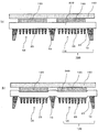
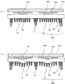
- (A) is a schematic sectional drawing which shows the state before adhering a vapor deposition mask and a vapor deposition target object, (b) adheres a vapor deposition mask and a vapor deposition target object using the magnetism of a magnetic board. It is a schematic sectional drawing which shows a state at the time. It is a schematic sectional drawing of the example of a comparison which shows a state when the vapor deposition mask and the vapor deposition target object are closely_contact
- (A)-(c) is a front view when the magnetic plate is viewed in plan.
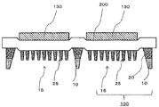
- FIG. 1 It is a schematic sectional drawing which shows an example before the vapor deposition mask and vapor deposition object are closely_contact
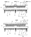
- (A) (b) is a schematic sectional drawing which shows an example of the state before making a vapor deposition mask and a vapor deposition target object contact
- FIG. 1 It is a front view when the vapor deposition mask of an example used for formation of the vapor deposition pattern of one Embodiment is planarly viewed from the metal mask side. It is a figure which shows the state which divided the magnitude
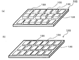
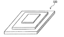
- (A), (b) is a perspective view which shows an example of the pressing plate integral type pushing member.
- (A) is a schematic sectional drawing which shows the state before adhering a vapor deposition mask and a vapor deposition target object
- (b) is a schematic sectional drawing which shows a state when a vapor deposition mask and a vapor deposition target object are stuck. It is.
- a method for forming a vapor deposition pattern according to an embodiment of the present disclosure uses a vapor deposition mask provided with a plurality of openings corresponding to a pattern to be vapor-deposited.
- a method of forming a vapor deposition pattern on a vapor deposition object as shown in FIGS. 1A and 1B, a vapor deposition mask 100 on one surface side (lower surface side in the illustrated form) of the vapor deposition object 200.
- the magnetic plate 150 is disposed on the other surface side (the upper surface side in the illustrated form) of the vapor deposition object 200, and the vapor deposition mask 100 and the vapor deposition object 200 are brought into close contact with each other using the magnetism of the magnetic plate 150.
- An adhesion process including a deposition pattern forming process in which a deposition material released from a deposition source is attached to the deposition target object 200 through the opening 25 and a deposition pattern is formed on the deposition target object 200 after the adhesion process.
- a pushing member 130 between the evaporation object 200 and the magnetic plate 150 is arranged, it is characterized in that to close contact with the evaporation object 200 and the deposition mask 100.
- FIG. 1A is a schematic cross-sectional view showing a state before the vapor deposition mask 100 and the vapor deposition target 200 are in close contact with each other
- FIG. 1B is a diagram in which the vapor deposition mask 100 and the vapor deposition target 200 are in close contact with each other. It is a schematic sectional drawing which shows a state when letting it be made.
- a deposition mask 100 containing a metal is disposed on one surface side of the deposition object 200, and a magnetic plate 150 is disposed on the other surface side of the deposition object 200.
- the vapor deposition mask 100 and the vapor deposition object 200 are brought into close contact with each other using the magnetism of the magnetic plate 150.
- the formation method of the vapor deposition pattern of one Embodiment arrange
- the pressing member 130 is appropriately disposed between the vapor deposition object 200 and the magnetic plate 150, whereby the vapor deposition mask 100 and the vapor deposition object. 200 can be brought into close contact with each other without a gap, and a high-definition vapor deposition pattern can be formed.
- the pushing member 130 is not arranged for the adhesion between the vapor deposition mask 100 and the vapor deposition target 200 when the vapor deposition mask 100 and the vapor deposition target 200 are brought into close contact using the magnetism of the magnetic plate 150.
- the advantages of the method for forming a vapor deposition pattern according to an embodiment will be described.
- the metal mask 10 provided with the slit 15 and a pattern formed by deposition at the position overlapping the slit 15 are supported.
- the vapor deposition mask 100 in which the resin mask 20 provided with a plurality of openings 25 is laminated will be described.
- the vapor deposition mask 100 is disposed on one surface side of the vapor deposition target object 200, the magnetic plate 150 is disposed on the other surface side of the vapor deposition target object 200, and the magnetic plate 150 is utilized to utilize the magnetic plate.
- 150 and the vapor deposition mask 100 are attracted, and thereby the vapor deposition mask 100 and the vapor deposition object 200 are brought into close contact with each other.
- the region that can be attracted by the magnetic plate 150 is a region that overlaps with a portion made of a metal material in the thickness direction, that is, a metal portion that is a non-slit region of the metal mask 10.
- a metal portion that is a non-slit region of the metal mask 10 may be simply referred to as a “metal portion”.
- a metal portion Is a region that overlaps in the thickness direction and is made of a resin material in the thickness direction. In the region where only the resin mask 20 and the magnetic plate 150 overlap, the vapor deposition mask 100 and the magnetic plate 150 cannot be attracted.
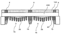
- FIG. 2 is a comparative example that does not satisfy the conditions of the adhesion process of the deposition pattern forming method according to the embodiment, and the deposition mask 130 is not disposed between the deposition target 200 and the magnetic plate 150.
- It is a schematic sectional drawing which shows a state when 100 and the vapor deposition target object 200 are stuck.
- the vapor deposition mask 100 is formed by laminating the metal mask 10 provided with the slit 15 and the resin mask 20 provided with the plurality of openings 25 corresponding to the pattern formed by vapor deposition at the position overlapping the slit 15.
- the magnetic plate 150 can be attracted in a region where the metal part of the vapor deposition mask and the magnetic plate 150 overlap in the thickness direction (region overlapped in the thickness direction with the region indicated by reference sign X in FIG. 2).
- a region that overlaps only with the resin mask 20 made of a resin material cannot be attracted by the magnetic plate 150. Therefore, in a region that cannot be attracted to the magnetic plate 150, that is, in a portion where the slit 15 of the metal mask 10 and the deposition target 200 overlap in the thickness direction, there is a gap between the deposition mask 100 and the deposition target 200. It tends to occur.
- a gap is generated between the vapor deposition mask 100 and the vapor deposition object 200 at a position overlapping the region of the vapor deposition mask 100 that cannot be attracted by the magnetic plate 150 in the thickness direction.
- the pressing step 130 is arranged between the vapor deposition object 200 and the magnetic plate 150 in the adhesion step, and the vapor deposition mask 100 and the vapor deposition object 200 are in close contact with each other.
- the vapor deposition object 200 is obtained.
- the deposition object 200 can be pushed into the deposition mask 100 side by the pushing member 130 arranged between the magnetic plate 150 and the magnetic plate 150.
- the vapor deposition object 200 pushed into the vapor deposition mask 100 side serves to fill a gap between the vapor deposition mask 100 and the vapor deposition object 200, and thereby the vapor deposition mask 100 and the vapor deposition are formed in a region overlapping the pushing member 130 in the thickness direction. Generation of a gap between the object 200 and the object 200 can be suppressed.
- FIG. 1B is a schematic cross-sectional view showing a state in which the deposition object 200 is pushed by the pushing member 130.
- the cross-sectional shape in the thickness direction of the vapor deposition object 200 at the portion pushed by the push member 130 is trapezoidal, but the material of the vapor deposition object 200 and the push member 130,
- the vapor deposition object 200 can be pushed in according to the shape of the pushing member 130 (see FIG. 11 described later).
- the vapor deposition object 200 can also be pushed in so that the cross-sectional shape in the thickness direction of the vapor deposition object 200 at the portion pushed by the pushing member 130 becomes an arc shape (not shown).
- the metal mask 10 provided with the slit 15 and the resin mask 20 provided with a plurality of openings 25 corresponding to the pattern to be vapor-deposited at a position overlapping the slit 15 are laminated as the vapor deposition mask 100.
- the vapor deposition mask 100 is described as an example, the form of the vapor deposition mask 100 used in the vapor deposition pattern forming method of one embodiment and the constituent members of the vapor deposition mask 100 are not limited in any way.
- a vapor deposition mask made of only a metal material can be used as the vapor deposition mask 100.
- the vapor deposition mask 100 When the vapor deposition mask 100 composed only of the metal material is used, the vapor deposition mask 100 can be attracted to the magnetic plate 150 in the entire region of the vapor deposition mask 100, and compared with the vapor deposition mask 100 including a resin material as a constituent member. Adhesion between the vapor deposition mask 100 and the vapor deposition object when the 100 and the magnetic plate 150 are attracted can be increased. However, even in the vapor deposition mask 100 made of only a metal material, the vapor deposition mask 100 and the magnetic plate 150 may not be sufficiently attracted depending on the ratio of the metal portion or the metal material. This is because a gap may be formed between the object 200 and the object 200.
- the method for forming a vapor deposition pattern according to an embodiment is suitable when the vapor deposition mask 100 in which a resin material is included in its constituent members is used. Specifically, when the vapor deposition mask 100 and the magnetic plate 150 are attracted, the vapor deposition mask 100 having a region that cannot be attracted to the magnetic plate 150, that is, the vapor deposition mask 100 made of only a resin material, as described above. Moreover, it is suitable when using the vapor deposition mask 100 in which the resin mask 20 and the metal mask 10 are laminated.
- the frame portion of the metal frame and the magnetic plate 150 can be attracted by using a vapor deposition mask with a metal frame in which a vapor deposition mask made of only a resin material is fixed to the metal frame.
- the metal frame will be described later.
- the arrangement position of the pushing member 130 is not particularly limited.
- the vapor deposition mask 100 and the vapor deposition target object 200 are brought into close contact with each other, the position where the adhesion between the vapor deposition mask 100 and the vapor deposition target object 200 is insufficient is overlapped. What is necessary is just to arrange.
- the vapor deposition mask 100 is disposed between the vapor deposition object 200 and the magnetic plate 150 at a position overlapping the slit 15 of the metal mask 10.
- a plurality of pushing members 130 may be arranged, and as shown in FIG. 3, one pushing member 130 is arranged. May be.
- the material of the pushing member 130 is not limited in any way, and may be a metal material, a resin material, a ceramic material, a glass material, or any other material. Among them, the resin material is preferable in that the vapor deposition object in contact with the pressing member 130 can be uniformly pressed and a sufficient pressing effect can be obtained as compared with the metal material.
- a resin material a polyimide resin etc. can be mentioned, for example.
- the shape of the pushing member 130 on the side in contact with the vapor deposition object 200 may be an R shape, in other words, the shape on the side of the pushing member 130 may have a curvature (not shown).
- a curvature there is no restriction
- the pushing member 130 and the vapor deposition object are obtained.
- the total area of the contacting portions is preferably 10% or more, more preferably 25% or more, and particularly preferably 85% or more.
- the area of the portion where one pushing member 130 is in contact with the vapor deposition object 200 in contact with the one pushing member 130 is preferably 200 mm 2 or more.
- the thickness of the push-in member 130 is not particularly limited, and can be appropriately set in consideration of the size of a gap that can be generated between the vapor deposition mask 100 and the vapor deposition object 200.
- the thickness of the pushing member 130 as an example is about 0.01 mm to 2 mm, 0.05 mm to 1 mm, and 0.1 mm to 0.7 mm.
- the magnetic plate 150 disposed on the pushing member 130 or a pressing plate 135 described later is a plate piece formed of a magnetic material, and a conventionally known material that can be attracted to the metal material, for example, the metal mask 10 is used.
- the metal portion of the metal mask 10 or when using the vapor deposition mask with a metal frame formed by fixing the vapor deposition mask 100 to the metal frame, attract the frame portion of the metal frame.
- Conventionally known materials that can be used can be appropriately selected and used.
- a magnet, a magnet sheet obtained by mixing a magnetic material with synthetic rubber, and the like can be given.
- the magnetic plate 150 in the vapor deposition pattern forming method of one embodiment, at least a part of the surface of the pressing member 130 or at least a part of the surface of the pressing plate 135 described later is covered, and The magnetic plate 150 is arranged so that the metal portion of the vapor deposition mask and the effective portion of the magnetic plate 150 overlap in the thickness direction.
- the magnetic plates 150 are arranged so as to overlap in the thickness direction.
- the magnetic plate 150 can be arranged so that the metal portion of the vapor deposition mask and the frame portion of the metal frame overlap the effective portion of the magnetic plate 150 in the thickness direction.
- the magnetic plate is disposed so that the metal portion of the vapor deposition mask or the frame portion of the metal frame and the effective portion of the magnetic plate 150 overlap in the thickness direction. This is because when the effective portion of the magnetic plate 150 does not overlap in the thickness direction, the vapor deposition mask 100 and the magnetic plate 150 cannot be attracted using the magnetic force of the magnetic plate.
- FIG. 1 when the magnetic plate 150 is viewed in plan, the shape as shown in FIGS. 4A and 4B is a shape in which a through hole is provided so as to leave an effective portion of the magnetic plate in part, FIG. As shown to (c), it can be set as arbitrary shapes, such as the shape which makes the whole area
- the outer shape of the magnetic plate 150 when viewed in plan is a rectangular shape, but may be a polygonal shape such as a rhombus or a shape having a curvature such as a circle or an ellipse. It may be.
- the thickness of the magnetic plate 150 may be determined in consideration of the magnetic force etc. of the magnetic plate 150, and is not particularly limited, but as an example, it is about 1 mm to 30 mm, preferably about 10 mm to 25 mm.
- one large magnetic plate is provided so as to collectively cover the surfaces of the plurality of pushing members 130 if the above conditions are satisfied.
- 150 (see FIG. 1) may be disposed, and a magnetic plate 150 may be disposed for each pushing member 130 as shown in FIG.
- the magnetic plate 150 when the magnetic plate 150 provided with the through hole is used, depending on the position of the through hole provided in the magnetic plate 150, the magnetic plate 150 is used.
- the vapor deposition object 200 When the magnetic plate 150 and the vapor deposition mask 100 are attracted, the vapor deposition object 200 may not be pushed into the vapor deposition mask 100 side when the effective portion of the material and the surface of the pushing member 130 do not overlap in the thickness direction. .
- the deposition target 200 cannot be pushed into the deposition mask 100 side when the magnetic plate 150 and the deposition mask 100 are attracted.
- a pressing plate 135 that overlaps at least a part of the surface of the pressing member 130 and an effective portion of the magnetic plate 150 in the thickness direction is pressed. It is preferable to arrange between 130 and the magnetic plate 150 so that the vapor deposition mask 100 and the vapor deposition object 200 are brought into close contact with each other.
- the shape of the magnetic plate 150 for example, the shape when the magnetic plate 150 is viewed in plan view, is the shape shown in FIGS. 4 (a) and 4 (b).
- the pushing member 130 can be pushed into the deposition object 200 side by the holding plate 135.
- the pushing member 130 can be pushed into the deposition object 200 side. Further, even when the shape of the magnetic plate 150 in plan view is as shown in FIG. 4C, as shown in FIG. 6B, the gap between the pushing member 130 and the magnetic plate 150 is shown.
- a pressing plate 135 may be disposed.
- a pressing plate integrated with a pressing plate 140 is formed by fixing one or a plurality of pressing members 130 to the pressing plate 135 (in the illustrated form, a plurality of pressing members 130 are fixed to the pressing plate 135). It can also be used.
- the plurality of pressing members 130 can be arranged on the deposition target 200 in one operation. The productivity can be improved as compared with the case where the plurality of pushing members 130 are individually arranged on the vapor deposition target 200.
- each pressing member 130 is integrated with the pressing plate 135, so that the pressing member 130 has more than the plurality of pressing members 130 arranged individually. It has the advantage of being difficult to slip.
- the pressing plate 135 is integrated.
- the pressing plate 135 is not easily in direct contact with the deposition target 200, and even when the pressing plate 135 and the deposition target 200 are in contact with each other, the pressing plate 135 is not touched.
- the strength of pushing the vapor deposition object 200 toward the vapor deposition mask 100 is weak. That is, the pressing plate 135 does not directly act on the pushing of the deposition target by the pushing member 130, or the degree of the action is small.
- the material of the pressing plate 135 is not particularly limited, but a material that does not interfere with the magnetic force of the magnetic plate 150 is preferable.
- a pressing plate made of a non-magnetic material is preferable.
- the nonmagnetic material include aluminum, carbon, and glass.
- the heat applied to the vapor deposition mask 100 is released during vapor deposition using the vapor deposition pattern forming method of one embodiment. If it does, it will serve as a cooling plate for cooling the vapor deposition mask, and it is possible to prevent the vapor deposition mask 100 from expanding due to heat during vapor deposition.
- the thickness of the pressing plate 135 is not particularly limited, but as an example, it is about 1 mm to 30 mm.
- the pushing member 130 fixed to the pressing plate 135 can be appropriately selected from those described above, and detailed description thereof is omitted here.
- the push-in member 130 will be described by taking the vapor deposition mask 100 used in the vapor deposition pattern forming method of one embodiment as an example.
- a vapor deposition mask used in the vapor deposition pattern forming method of one embodiment
- a vapor deposition mask (hereinafter, referred to as a vapor deposition mask according to an embodiment) used in the method for forming a vapor deposition pattern according to an embodiment includes a metal mask 10 having slits 15 and the slits as illustrated in FIG. And a resin mask 20 having an opening 25 corresponding to a pattern to be formed by vapor deposition at a position overlapping with the resin mask 20.
- FIG. 7 is a front view when the vapor deposition mask used for the manufacturing method of the vapor deposition mask with a frame of one Embodiment is planarly viewed from the metal mask side
- FIG.7 (b) is A of (a).
- -A is a schematic cross-sectional view.
- the opening shape of the opening 25 is rectangular, but the opening shape is not particularly limited, and may be any shape as long as it corresponds to the pattern to be deposited.
- the opening shape of the opening 25 may be a diamond shape or a polygonal shape, or may be a shape having a curvature such as a circle or an ellipse.
- the rectangular or polygonal opening shape is a preferable opening shape of the opening 25 in that the light emitting area can be increased as compared with the opening shape having a curvature such as a circle or an ellipse.
- the material of the resin mask 20 is not limited.
- a high-definition opening 25 can be formed by laser processing or the like, and a lightweight material with a small dimensional change rate and moisture absorption rate over time and heat is used.
- Such materials include polyimide resin, polyamide resin, polyamideimide resin, polyester resin, polyethylene resin, polyvinyl alcohol resin, polypropylene resin, polycarbonate resin, polystyrene resin, polyacrylonitrile resin, ethylene vinyl acetate copolymer resin, ethylene- Examples thereof include vinyl alcohol copolymer resin, ethylene-methacrylic acid copolymer resin, polyvinyl chloride resin, polyvinylidene chloride resin, cellophane, and ionomer resin.
- a resin material having a thermal expansion coefficient of 16 ppm / ° C. or less is preferable, a resin material having a moisture absorption rate of 1.0% or less is preferable, and a resin material having both conditions is particularly preferable.
- this resin material By using this resin material as a resin mask, the dimensional accuracy of the opening 25 can be improved, and the dimensional change rate and moisture absorption rate over time can be reduced.
- the thickness of the resin mask 20 is not particularly limited, but in the case of further improving the effect of suppressing the generation of shadows, the thickness of the resin mask 20 is preferably 25 ⁇ m or less, and more preferably less than 10 ⁇ m. Although there is no particular limitation on the preferable range of the lower limit value, when the thickness of the resin mask 20 is less than 3 ⁇ m, defects such as pinholes are likely to occur, and the risk of deformation and the like increases. In particular, by setting the thickness of the resin mask 20 to 3 ⁇ m or more and less than 10 ⁇ m, more preferably 4 ⁇ m or more and 8 ⁇ m or less, it is possible to more effectively prevent the influence of shadows when forming a high-definition pattern exceeding 400 ppi. .
- the resin mask 20 and the metal mask 10 to be described later may be bonded directly or via an adhesive layer, but the resin mask 20 and the metal mask via an adhesive layer. 10 is bonded, it is preferable that the total thickness of the resin mask 20 and the pressure-sensitive adhesive layer is within the range of the preferable thickness.
- the shadow is a target vapor deposition because a part of the vapor deposition material released from the vapor deposition source does not reach the vapor deposition target by colliding with the slit of the metal mask or the inner wall surface of the opening of the resin mask. This is a phenomenon in which an undeposited portion having a film thickness smaller than the film thickness occurs.
- the cross-sectional shape of the opening 25 there is no particular limitation on the cross-sectional shape of the opening 25, and the end faces facing each other of the resin mask forming the opening 25 may be substantially parallel to each other.
- the cross-sectional shape has a shape that expands toward the vapor deposition source.
- the taper angle can be appropriately set in consideration of the thickness of the resin mask 20 and the like, but is a straight line connecting the lower bottom tip of the resin mask opening and the upper bottom tip of the resin mask opening.
- the angle formed by the bottom surface of the resin mask in other words, in the cross section in the thickness direction of the inner wall surface constituting the opening 25 of the resin mask 20, the side that does not contact the inner mask of the opening 25 and the metal mask 10 of the resin mask 20 Is preferably in the range of 5 ° to 85 °, more preferably in the range of 15 ° to 75 °, and 25 °. More preferably, it is in the range of ⁇ 65 °. In particular, within this range, an angle smaller than the vapor deposition angle of the vapor deposition machine to be used is preferable.
- the end surface forming the opening 25 has a linear shape, but is not limited to this, and has an outwardly convex curved shape, that is, the entire opening 25.
- the shape may be a bowl shape.
- Metal mask As shown in FIG. 7B, the metal mask 10 is laminated on one surface of the resin mask 20.
- the metal mask 10 is made of metal and has slits 15 extending in the vertical direction or the horizontal direction.
- the slit 15 is synonymous with the opening.
- the slits extending in the vertical direction and the horizontal direction may be arranged in a plurality of rows in the vertical direction and the horizontal direction, and the slits extending in the vertical direction are arranged in a plurality of rows in the horizontal direction.
- the slits extending in the horizontal direction may be arranged in a plurality of rows in the vertical direction. Further, only one row may be arranged in the vertical direction or the horizontal direction.
- vertical direction and lateral direction refer to the vertical and horizontal directions of the drawing, and are any of the longitudinal direction and the width direction of the vapor deposition mask, resin mask, and metal mask. May be.
- the longitudinal direction of the vapor deposition mask, the resin mask, and the metal mask may be “vertical direction”
- the width direction may be “vertical direction”.
- shape of the vapor deposition mask when viewed in plan is a rectangular shape is described as an example, but other shapes, for example, a circular shape, a polygonal shape such as a rhombus shape, etc. It is good.
- the longitudinal direction, the radial direction, or an arbitrary direction of the diagonal line is defined as a “longitudinal direction”, and a direction orthogonal to the “longitudinal direction” is referred to as a “width direction (sometimes referred to as a short direction)”. do it.
- the material of the metal mask 10 is not particularly limited, and any conventionally known material can be appropriately selected and used in the field of the evaporation mask, and examples thereof include metal materials such as stainless steel, iron-nickel alloy, and aluminum alloy. . Among them, an invar material that is an iron-nickel alloy can be suitably used because it is less deformed by heat.
- the thickness of the metal mask 10 is not particularly limited, it is preferably 100 ⁇ m or less, more preferably 50 ⁇ m or less, and more preferably 35 ⁇ m or less in order to more effectively prevent the occurrence of shadows. Particularly preferred. When the thickness is less than 5 ⁇ m, the risk of breakage and deformation increases and handling tends to be difficult.
- the shape of the opening of the slit 15 when viewed in plan is a rectangular shape, but the opening shape is not particularly limited, and the opening shape of the slit 15 is trapezoidal. Any shape such as a circular shape may be used.
- the cross-sectional shape of the slit 15 formed in the metal mask 10 is not particularly limited, it is preferably a shape having a spread toward the vapor deposition source as shown in FIG. More specifically, the angle formed by the straight line connecting the lower bottom tip of the slit 15 of the metal mask 10 and the upper bottom tip of the slit 15 of the metal mask 10 and the bottom surface of the metal mask 10, in other words, In the thickness direction cross section of the inner wall surface constituting the slit 15 of the metal mask 10, the angle formed by the inner wall surface of the slit 15 and the surface of the metal mask 10 on the side in contact with the resin mask 20 (in the illustrated embodiment, the lower surface of the metal mask).
- the method for laminating the metal mask 10 on the resin mask is not particularly limited, and the resin mask 20 and the metal mask 10 may be bonded together using various adhesives, or a resin mask having self-adhesiveness may be used. . Resin mask 20 and metal mask 10 may have the same size or different sizes. If the resin mask 20 is made smaller than the metal mask 10 and the outer peripheral portion of the metal mask 10 is exposed in consideration of the optional fixing to the frame thereafter, the metal mask 10 It is preferable because it can be easily fixed to the frame.
- the metal mask 10 may be formed by processing a metal plate, or may be formed using a plating method or the like. Further, it may be formed by other methods.
- the vapor deposition mask shown in FIG. 8 is arranged on one surface of the vapor deposition object 200, the magnetic plate 150 is arranged on the other surface of the vapor deposition object 200, and the magnetism of the magnetic plate 150 is used. Then, the size of the gap that may be generated between the vapor deposition mask 100 and the vapor deposition target object 200 when the vapor deposition mask 100 and the vapor deposition target object 200 are brought into close contact with each other will be described together with a preferable form of the pushing member 130.
- FIG. 8 is a front view when the vapor deposition mask 100 is viewed in plan from the metal mask side.
- the size of the gap generated between the vapor deposition mask 100 and the vapor deposition target 200 is as follows. In other words, as it goes from the outer periphery to the inner side of the vapor deposition mask 100, in other words, the vapor deposition object 200 becomes larger from the outer periphery to the inner side. In particular, this tendency increases as the vapor deposition mask 100 increases in size. In summary, the gap tends to increase in the vicinity of the center of the deposition mask when the deposition mask 100 is viewed in plan. This is considered due to the weight of the vapor deposition mask 100. FIG.
- FIG. 9 is a diagram showing a state in which the vapor deposition mask shown in FIG. 8 is viewed in plan from the metal mask 10 side, and a gap that may be generated between the vapor deposition mask 100 and the vapor deposition object 200 for each region overlapping each slit 15.
- a gap that may be generated between the vapor deposition mask 100 and the vapor deposition object 200 for each region overlapping each slit 15.
- the size of the gap increases in the order of “A”, “B”, and “C”.
- the thickness of the gap between the vapor deposition mask 100 and the vapor deposition target 200 is taken into consideration and the thicknesses are appropriately different. It is preferable to arrange the member 130 (“preferable pushing member form A”). Specifically, as shown in FIG. 10A, it is preferable to dispose a pushing member 130 that increases in thickness from the outer periphery of the vapor deposition target 200 toward the inside. More specifically, a thick pushing member 130 is arranged in a region corresponding to the above “C”, and the pushing member 130 having a thin thickness continuously or discontinuously with “B” and “A” is arranged. It is preferable to arrange them.
- the thickness of the pushing member 130 referred to here means the apex of the pushing member that is farthest from the bottom surface of the pushing member 10 or the height to the top surface.
- FIG. 10A is a perspective view showing an example of a pressing plate integrated pressing member 140. A thickness of the pressing member 140 is increased on the pressing plate 135 so that the pressing member increases in thickness from the outer periphery toward the inner side. A plurality of different pushing members 130 are fixed.
- the above is an example when a plurality of pushing members 130 having different thicknesses are arranged, and a plurality of pushing members 130 having different thicknesses can be appropriately arranged in accordance with the size of the gap and the like.
- the pushing member with a small thickness may be arranged from the outer periphery of the vapor deposition target 200 toward the inside, and a plurality of pushing members 130 having different thicknesses may be arranged at random.
- the thickness of a some pushing member can also be made constant.
- FIG. 12 focuses on one of the regions partitioned by the slits, and shows the size of the gap generated between the deposition mask 100 and the deposition object 200 at a position overlapping the partitioned region in the thickness direction.
- FIG. 5 is a partial schematic diagram in which levels are classified by “A ′”, “B ′”, and “C ′”. The size of the gap increases in the order of “A ′”, “B ′”, and “C ′”. As shown in the figure, in the region partitioned by the slit 15, the size of the gap generated between the vapor deposition mask 100 and the vapor deposition object is smaller as it is closer to the metal portion of the metal mask 10, and away from the metal portion. The gap tends to increase with time.
- the vapor deposition mask 100 and the magnetic plate 150 are attracted to a metal portion that is a slit non-formation region of the metal mask 10, the vapor deposition mask 100 and the magnetic plate 150 are directly attracted. In the vicinity of the metal part, there is no gap between the vapor deposition mask 100 and the vapor deposition object 200, or the gap is small and far from the metal part where the vapor deposition mask 100 and the magnetic plate 150 are directly attracted. As it becomes, the gap tends to increase.
- the size of the gap in the partitioned region is taken into consideration and continuously from the outer periphery toward the inside.
- a pushing member 130 whose thickness changes discontinuously (“preferred pushing member form B”).
- FIG. 13 it is preferable to use a pushing member 130 whose thickness increases continuously or discontinuously from the outer periphery toward the inside.
- the shape on the side in contact with the vapor deposition target 200 described above is an R shape, in other words, the shape on the side in contact has a curvature. Can be mentioned.
- a pushing member whose thickness changes discontinuously a pushing member whose thickness changes stepwise as shown in FIG. 13 can be cited.
- FIG. 11A is a schematic cross-sectional view showing a state before the vapor deposition mask 100 and the magnetic plate 150 are attracted
- FIG. 11B is a diagram when the vapor deposition mask 100 and the vapor deposition object 200 are brought into close contact with each other.
- It is a schematic sectional drawing which shows a state.
- a pushing member 130 whose thickness changes continuously or discontinuously from the outer periphery to the inside between the vapor deposition object 200 and the magnetic plate 150 (the form shown in FIG. 13). Then, a pushing member 130) whose thickness changes discontinuously is disposed.
- FIG. 13 a pushing member 130 whose thickness changes discontinuously is disposed.
- the vapor deposition mask 100 and the magnetic plate 150 are attracted by using the pushing member 130 whose thickness changes continuously or discontinuously from the outer periphery toward the inner side.
- the pushing amount of the deposition object pushed by the pushing member 130 can be changed. Specifically, in a region where a gap is likely to occur, the amount of pushing of the deposition object is increased, while in a region where the gap that can be generated is small, the amount of pushing of the deposition object is reduced.
- the deposition mask 100 and the deposition object 200 can be brought into close contact with each other by changing the push-in amount corresponding to the size. The same applies to the case of “Preferred pushing member form A”.
- the pushing member 130 of the above preferred form overlaps the region partitioned by the slit 15 when the size of the gap changes in the region partitioned by the slit 15 as shown in FIG.
- This is an example of arrangement at a position, and in consideration of the size of the gap in the area partitioned by the slit 15, the position overlapping with the area partitioned by the slit 15 is appropriately, continuously, or non-
- the pushing member 130 whose thickness changes continuously can be arranged.
- a pushing member whose thickness decreases continuously or discontinuously from the outer periphery of the vapor deposition target 200 may be arranged, or a pushing member 130 whose thickness changes randomly may be arranged. .
- the pressing plate 140 is integrated with the pressing plate 140.
- the pressing plate 135 is not used and the slit 15 is used.
- the pushing members 130 may be individually arranged at positions that overlap with the regions partitioned in the thickness direction.
- one pushing member 130 is disposed at a position that overlaps the area partitioned by the slit 15 in the thickness direction, but the position that overlaps the area partitioned by the slit 15 in the thickness direction.
- a plurality of pushing members 130 can be arranged (not shown).
- the pushing member 130 may be arranged at a position that overlaps with a portion where a gap may occur in the area divided by the slit 15.
- the pressing member 130 when used so that the side length of the pushing member when viewed in plan is 50% or more, preferably 70% or more of each side length of the partitioned area, when viewed in plan. It is preferable to arrange so that the center of the pushing member overlaps the center of the region defined by the slit.
- the vapor deposition mask 100 of the embodiment (A) is a vapor deposition mask for simultaneously forming vapor deposition patterns for a plurality of screens, and a plurality of slits 15 are formed on one surface of the resin mask 20.
- the resin mask 20 is provided with openings 25 necessary for forming a plurality of screens, and each slit 15 is provided at a position overlapping at least one entire screen. It is characterized by.
- the vapor deposition mask 100 of the embodiment (A) is a vapor deposition mask used for simultaneously forming vapor deposition patterns for a plurality of screens, and the vapor deposition patterns corresponding to a plurality of products are simultaneously formed with one vapor deposition mask 100. Can do.
- the “opening” referred to in the vapor deposition mask of the embodiment (A) means a pattern to be produced using the vapor deposition mask 100 of the embodiment (A).
- the vapor deposition mask is an organic layer in an organic EL display.
- the shape of the opening 25 is the shape of the organic layer.
- “one screen” includes an assembly of openings 25 corresponding to one product.
- an aggregate of organic layers that is, an aggregate of openings 25 serving as an organic layer is “one screen”.
- the “one screen” is arranged on the resin mask 20 for a plurality of screens at predetermined intervals. Yes. That is, the resin mask 20 is provided with openings 25 necessary for forming a plurality of screens.
- the metal mask 10 provided with a plurality of slits 15 is provided on one surface of the resin mask, and each slit is provided at a position overlapping with at least one entire screen. It is characterized by that.
- the length is the same as the length of the slit 15 in the vertical direction, and is the same as the metal mask 10.
- metal wire portions having a thickness may be collectively referred to simply as metal wire portions.
- the vapor deposition mask 100 of the embodiment (A) when the size of the opening 25 necessary to configure one screen or the pitch between the openings 25 configuring one screen is narrowed, for example, exceeds 400 ppi. Even when the size of the openings 25 and the pitch between the openings 25 are extremely small in order to form a screen, it is possible to prevent interference due to the metal line portion and to form a high-definition image. It becomes possible.
- FIGS. In the form shown in the figure, a region closed by a broken line is one screen.
- a small number of openings 25 are aggregated as one screen.
- the present invention is not limited to this form.
- one opening 25 is defined as one pixel
- one screen There may be an opening 25 of several million pixels.
- one screen is constituted by an aggregate of openings 25 in which a plurality of openings 25 are provided in the vertical and horizontal directions.
- one screen is constituted by an aggregate of openings 25 in which a plurality of openings 25 are provided in the horizontal direction.
- one screen is constituted by an aggregate of openings 25 in which a plurality of openings 25 are provided in the vertical direction. 14 to 16, a slit 15 is provided at a position overlapping the entire screen.
- the slit 15 may be provided at a position that overlaps with only one screen, and is provided at a position that overlaps with two or more entire screens, as shown in FIGS. It may be.
- a slit 15 is provided at a position overlapping the entire two screens that are continuous in the horizontal direction.
- the slit 15 is provided at a position overlapping the entire three screens that are continuous in the vertical direction.
- the pitch between the openings 25 constituting one screen and the pitch between the screens will be described.
- the pitch between the openings 25 constituting one screen and the size of the openings 25, can be set as appropriate according to the pattern to be deposited.
- the horizontal pitch (P1) and vertical pitch (P2) of the adjacent openings 25 in the openings 25 constituting one screen are about 60 ⁇ m. It becomes.
- the size of the opening is about 500 ⁇ m 2 to 1000 ⁇ m 2 .
- one opening 25 is not limited to corresponding to one pixel. For example, depending on the pixel arrangement, a plurality of pixels can be integrated into one opening 25.
- the horizontal pitch (P3) between the screens and the vertical pitch (P4) are not particularly limited, but as shown in FIG. 14, when one slit 15 is provided at a position overlapping the entire screen, A metal line portion exists between the screens. Accordingly, the vertical pitch (P4) and horizontal pitch (P3) between the screens are smaller than the vertical pitch (P2) and horizontal pitch (P1) of the openings 25 provided in one screen. In this case, or when they are substantially equivalent, the metal wire portion existing between the screens is easily broken. Therefore, in consideration of this point, it is preferable that the pitch (P3, P4) between the screens is wider than the pitch (P1, P2) between the openings 25 constituting one screen. An example of the pitch (P3, P4) between the screens is about 1 mm to 100 mm. Note that the pitch between the screens means a pitch between adjacent openings in one screen and another screen adjacent to the one screen. The same applies to the pitch of 25 between the openings and the pitch between the screens in the vapor deposition mask of the embodiment (B) described later.
- the pitch between two or more screens provided at a position overlapping with one slit 15 may be substantially equal to the pitch between the openings 25 constituting one screen.
- grooves (not shown) extending in the vertical direction or the horizontal direction of the resin mask 20 may be formed in the resin mask 20.
- the resin mask 20 may thermally expand, which may cause changes in the size and position of the opening 25.
- the groove may be provided between the openings 25 constituting one screen or at a position overlapping with the openings 25, but is preferably provided between the screens.
- the groove may be provided only on one surface of the resin mask, for example, the surface in contact with the metal mask, or may be provided only on the surface not in contact with the metal mask. Alternatively, it may be provided on both surfaces of the resin mask 20.
- a groove extending in the vertical direction between adjacent screens may be formed, or a groove extending in the horizontal direction may be formed between adjacent screens. Furthermore, it is possible to form the grooves in a combination of these.
- the depth and width of the groove are not particularly limited. However, when the depth of the groove is too deep or too wide, the rigidity of the resin mask 20 tends to decrease, so this point is taken into consideration. It is necessary to set it. Further, the cross-sectional shape of the groove is not particularly limited, and may be arbitrarily selected in consideration of a processing method such as a U shape or a V shape. The same applies to the vapor deposition mask of the embodiment (B).
- the push members 130 used when the vapor deposition mask 100 and the vapor deposition target 200 are brought into close contact with each other using the vapor deposition mask of the embodiment (A) are appropriately selected. However, it is preferable to dispose the pushing member 130 at a position overlapping with one screen in the thickness direction so that the “preferable pushing member form A” and the “preferable pushing member form B” are obtained.
- the vapor deposition mask of embodiment (B) is demonstrated. As shown in FIG. 18, the vapor deposition mask of the embodiment (B) has one slit (one hole 16) on one surface of the resin mask 20 provided with a plurality of openings 25 corresponding to the pattern to be vapor deposited. ) Is laminated, and all of the plurality of openings 25 are provided at positions overlapping one hole 16 provided in the metal mask 10.
- the opening 25 referred to in the vapor deposition mask of the embodiment (B) means an opening necessary for forming the vapor deposition pattern on the vapor deposition target, and is not necessary for forming the vapor deposition pattern on the vapor deposition target.
- the portion may be provided at a position that does not overlap with one hole 16.
- FIG. 18 is a front view when the vapor deposition mask which shows an example of the vapor deposition mask of embodiment (B) is planarly viewed from the metal mask side.
- the metal mask 10 having one hole 16 is provided on the resin mask 20 having the plurality of openings 25, and all of the plurality of openings 25 are It is provided at a position overlapping with the one hole 16.
- the metal line portion between the openings 25 that is the same as the thickness of the metal mask or thicker than the thickness of the metal mask.
- the thickness of the metal mask 10 is The thickness can be increased until the durability and handling properties can be sufficiently satisfied, and the durability and handling properties can be improved while enabling the formation of a high-definition deposition pattern.
- the resin mask 20 in the vapor deposition mask of the embodiment (B) is made of resin, and as shown in FIG. 18, a plurality of openings 25 corresponding to the pattern for vapor deposition are provided at positions overlapping one hole 16. .
- the opening 25 corresponds to a pattern to be produced by vapor deposition, and the vapor deposition material released from the vapor deposition source passes through the opening 25 so that a vapor deposition pattern corresponding to the opening 25 is formed on the vapor deposition target.
- the openings are arranged in a plurality of rows in the vertical and horizontal directions is described. However, the openings may be arranged only in the vertical or horizontal direction.
- “One screen” in the vapor deposition mask 100 of the embodiment (B) means an aggregate of the openings 25 corresponding to one product, and one organic product is used when the one product is an organic EL display.
- An aggregate of organic layers necessary for forming an EL display, that is, an aggregate of openings 25 serving as an organic layer is “one screen”.
- the vapor deposition mask of the embodiment (B) may be composed of only “one screen” or may be a plurality of “one screen” arranged for a plurality of screens. When the screens are arranged, it is preferable that the openings 25 are provided with a predetermined interval for each screen unit (see FIG. 14 of the vapor deposition mask of the embodiment (A)).
- the metal mask 10 in the vapor deposition mask 100 of the embodiment (B) is made of metal and has one hole 16. Further, the one hole 16 is arranged at a position where it overlaps with all the openings 25 when viewed from the front of the metal mask 10, in other words, at a position where all the openings 25 arranged in the resin mask 20 can be seen. ing.
- a metal portion constituting the metal mask 10, that is, a portion other than one hole 16 may be provided along the outer edge of the vapor deposition mask 100 as shown in FIG. 18, and as shown in FIG.
- the size may be smaller than that of the resin mask 20 and the outer peripheral portion of the resin mask 20 may be exposed. Further, the size of the metal mask 10 may be made larger than that of the resin mask 20, and a part of the metal portion may protrude outward in the horizontal direction or in the vertical direction of the resin mask. In any case, the size of one hole 16 is smaller than the size of the resin mask 20.
- widths of W1 and W2 are narrow. As it becomes, durability and handling properties tend to decrease. Therefore, it is preferable that W1 and W2 have widths that can sufficiently satisfy durability and handling properties.
- an appropriate width can be appropriately set according to the thickness of the metal mask 10, as an example of a preferable width, both W1 and W2 are about 1 mm to 100 mm as in the metal mask of the vapor deposition mask of the embodiment (A). is there.
- the vapor deposition mask of the embodiment (B) since the metal mask 10 has one hole 16, the vapor deposition mask of the embodiment (B) and the magnetic plate 150 exist on the outer periphery of the metal mask 10. Since it is attracted only to the metal portion, the gap generated between the vapor deposition mask 100 and the vapor deposition object 200 tends to increase toward the inside of the vapor deposition mask 100 as compared with the vapor deposition mask of the above embodiment (A). is there. Therefore, when using the vapor deposition mask of embodiment (B), it is preferable to use the pushing member 130 having a relatively large thickness.
- a vapor deposition mask with metal frame As a vapor deposition mask used in the method for forming a vapor deposition pattern according to an embodiment, a vapor deposition mask with a metal frame in which the vapor deposition masks of various forms described above are fixed to a metal frame can be used.
- the vapor deposition mask 100 and the magnetic plate 150 can be attracted even in the frame portion of the metal frame, and coupled with the effect of the pushing member 130 described above, the vapor deposition mask 100 and the vapor deposition target The adhesion with the object 200 can be further increased.
- the vapor deposition mask 200 with a metal frame used in the vapor deposition pattern forming method of one embodiment may be one in which one vapor deposition mask 100 is fixed to a metal frame 60. As shown in FIG. 4, a plurality of vapor deposition masks 100 may be fixed to the metal frame 60.
- the metal frame 60 is a substantially rectangular frame member and has a through hole for exposing the opening 25 provided in the resin mask 20 of the vapor deposition mask 100 to be finally fixed to the vapor deposition source side.
- a frame made of a material other than a metal material for example, a frame made of a ceramic material, etc. Can also be used.
- the thickness of the metal frame is not particularly limited, but is preferably about 10 mm to 30 mm from the viewpoint of rigidity and the like.
- the width between the inner peripheral end face of the opening of the metal frame and the outer peripheral end face of the metal frame is not particularly limited as long as the metal frame and the metal mask of the vapor deposition mask can be fixed. A width of about 70 mm can be exemplified.
- a reinforcing frame 65 or the like is provided in the through hole region of the metal frame as long as exposure of the opening 25 of the resin mask 20 constituting the vapor deposition mask 100 is not hindered.
- the provided metal frame 60 may be used.
- the opening of the metal frame 60 may be divided by the reinforcing frame or the like.
- the vapor deposition mask 100 is fixed to the metal frame 60 even at a position where the reinforcement frame and the vapor deposition mask overlap. Can do.
- the vapor deposition mask with the metal frame and the magnetic plate 150 can be sufficiently attracted using the frame portion of the metal frame and the reinforcing frame 65, and the pushing member In combination with 130, the vapor deposition mask with metal frame and the vapor deposition object 200 can be sufficiently adhered to each other without a gap.
- the metal mask 10 provided with the slit 15 and the resin mask 20 provided with a plurality of openings 25 corresponding to the pattern to be vapor-deposited at positions overlapping the slit 15;
- the metal mask 10 is disposed in a part of the effective region of the other evaporation mask, for example, the resin mask 20 described above. It is also possible to use a deposited mask.
- a vapor deposition mask in which a plurality of metal masks are provided in the effective region of the resin mask 20 described above, or a vapor deposition mask in which a metal mask is disposed only in a region where rigidity is required can be given.
- region said here can mention the area
- a deposition mask 100 containing a metal is disposed on one side of the deposition target 200, a magnetic plate 150 is disposed on the other side of the deposition target 200, and the magnetic plate
- the vapor deposition mask 100 and the vapor deposition object 200 are brought into close contact with each other using the magnetism of 150, and is not limited to the vapor deposition mask described above. That is, any vapor deposition mask may be used as long as it is a vapor deposition mask containing metal.
- a vapor deposition mask containing a metal As a vapor deposition mask containing a metal, a vapor deposition mask in which the material of the resin mask 20 provided with a plurality of openings 25 corresponding to the pattern to be vapor-deposited is replaced with a metal material, or a plurality of openings corresponding to a pattern to be vapor-deposited.
- An evaporation mask composed only of a metal mask provided with a portion can be exemplified.
- the metal can be contained. It can also be set as the vapor deposition mask containing.
- the vapor deposition material released from the vapor deposition source is attached to the vapor deposition target surface of the vapor deposition target through the opening 25 provided in the vapor deposition mask 100 after the adhesion step. Is a step of forming a vapor deposition pattern.
- the vapor deposition method that can be used in the vapor deposition pattern forming method of one embodiment is not particularly limited.
- physical vapor deposition methods such as reactive sputtering, vacuum vapor deposition, ion plating, and electron beam vapor deposition ( Chemical Vapor Deposition, such as Physical Vapor Deposition), Thermal CVD, Plasma CVD, Photo CVD, and the like can be given.
- the vapor deposition pattern can be formed using a conventionally known vacuum vapor deposition apparatus or the like.
- a vapor deposition pattern is formed on the deposition surface of the vapor deposition pattern forming process.
- the adhesion process increases the adhesion between the vapor deposition mask 100 and the vapor deposition object 200 and suppresses the formation of a gap between the vapor deposition mask 100 and the vapor deposition object 200. Can do. Therefore, according to the deposition pattern forming method of one embodiment, in the deposition pattern forming process, when the deposition material released from the deposition source passes through the opening, the deposition material wraps around the gap to form a predetermined interval. It is possible to prevent the vapor deposition patterns that are to be formed from being connected to each other or to cause problems such as thickening of the vapor deposition pattern size, and a high-definition vapor deposition pattern can be formed.
- the vapor deposition pattern forming method is a vapor deposition pattern forming method in which a vapor deposition pattern is formed on a vapor deposition object using a vapor deposition mask provided with a plurality of openings corresponding to a vapor deposition pattern.
- the vapor deposition mask 100 is arranged on one surface side (the lower surface side in the illustrated form) of the vapor deposition target object 200, and the other surface side (the illustrated form).
- the pressing member 130 is disposed on the upper surface side), and the deposition object 200 is pushed into the deposition mask side 100 by the weight of the pushing member 130 to bring the deposition mask 100 and the deposition object 200 into close contact with each other.
- FIG. 23 and FIG. 24 are schematic cross-sectional views showing a state in which the vapor deposition mask and the vapor deposition object are brought into close contact with each other by using the pushing member 130 or the pushing plate-integrated pushing member 140.
- the method for forming a vapor deposition pattern according to another embodiment is different from the method for forming a vapor deposition pattern according to the above-described embodiment in that the magnetic plate 150 is not an essential constituent element.
- the method for forming a vapor deposition pattern of another embodiment is as follows: (I) The magnetic plate is not an essential component. (Ii) The pushing member is pushed in without using a magnetic plate.
- this method is different from the method for forming a vapor deposition pattern of the above-described embodiment, and is common to the method for forming a vapor deposition pattern of the above-described embodiment except for this difference. Therefore, in the method for forming a vapor deposition pattern according to another embodiment, various aspects described in the method for forming a vapor deposition pattern according to the above-described embodiment can be appropriately selected and used except for differences.
- the form of the pushing member, the arrangement position, and the like are common to the method for forming the vapor deposition pattern of the above-described embodiment.
- the magnetic plate is not an essential constituent element
- the pushing member 130 is disposed on the other surface side (the upper surface side in the illustrated form) of the vapor deposition object 200, and appropriate means.
- the pushing member 130 is pushed into the vapor deposition mask side 100 to bring the vapor deposition mask and the vapor deposition object into close contact. Therefore, in the vapor deposition pattern forming method according to another embodiment, a vapor deposition mask that does not contain metal, for example, a vapor deposition mask that includes only the resin mask 20 provided with the opening 25 corresponding to the pattern to be vapor deposited can be used. .
- the vapor deposition mask demonstrated by the formation method of the vapor deposition pattern of one embodiment above can also be used as it is.
- other conventionally known vapor deposition masks can be appropriately selected and used.
- a method for pushing the pushing member 130 disposed on the other surface side of the vapor deposition target 200 into the vapor deposition mask 100 side there is no particular limitation on a method for pushing the pushing member 130 disposed on the other surface side of the vapor deposition target 200 into the vapor deposition mask 100 side.
- the driving means is brought into contact with the pushing member 130, and the driving means brought into contact with the pushing member 130 is driven toward the vapor deposition mask 100, thereby pushing the pushing member. 130 can be pushed into the deposition mask 100 side.
- pushing the pushing member 130 into the vapor deposition mask side referred to in the present specification includes not only a form in which the pushing member 130 is pushed toward the vapor deposition mask 100 side but also a form in which the vapor deposition mask 100 is pushed toward the push member 130 side. It is.
- the vapor deposition mask 100 may be held by a driving unit, or the vapor deposition mask 100 and the driving unit may be brought into contact with each other, and the driving unit may be driven toward the pushing member 130 side.
- the mass and size of the pushing member 130 there is no particular limitation on the mass and size of the pushing member 130 in the case where the pushing member 130 is pushed into the deposition mask 100 side by the weight of the pushing member, but at least the deposition object 200 is deposited by the dead weight. Although it can be pushed into the mask 100 side, it only needs to have a mass or size.
- the mass and size of the pushing member 130 can be appropriately set depending on the material of the vapor deposition target 200, the thickness of the vapor deposition target 200, and the like.
- a material of the pushing member 130 for example, a material having a mass per unit volume of 2.0 g / cm 3 or more is preferably used, and a material of 2.5 g / cm 3 or more is more preferably used.
- the mass of each pushing member 130 may be 50 g or more. Preferably, it is 100 g or more.
- one or a plurality of pressing members 130 are fixed to the pressing plate 135 (in the illustrated embodiment, a plurality of pressing members 130 are fixed to the pressing plate 135).
- the use of the integrated push-in member 140 is preferable in that the overall mass can be increased. Further, the pushing member 130 can be accurately arranged on the other surface side of the vapor deposition target 200.
- a weight (not shown) is placed on the pushing member 130, the holding plate 135, or the pressing member integrated pressing member 140. It is possible to increase the force to push in.
- the pushing member 130 disposed on the other surface side of the vapor deposition object 200 can be pushed into the vapor deposition mask side using a drive mechanism.
- the drive mechanism may be capable of holding the push member 130 and having a function of moving the held push member 130 in an arbitrary direction.
- a pressing plate integrated pressing member (hereinafter referred to as a pressing plate integrated pressing member according to an embodiment) according to an embodiment of the present disclosure will be described.
- a vapor deposition mask is arranged on one surface side of the vapor deposition object
- a magnetic plate is arranged on the other surface side of the vapor deposition object, and the magnetic force of the magnetic plate
- the deposition object and the deposition mask are brought into close contact with each other, the deposition object is disposed between the deposition object and the magnetic plate, or (2) the deposition mask is provided on one surface side of the deposition object.
- the pressing member 140 is a pressing plate integrated type pressing member 140 provided with a plurality of pressing members 130. According to the pressing plate-integrated pressing member of one embodiment, the pressing plate-integrated pressing member is disposed between the vapor deposition object and the magnetic plate so that the vapor deposition mask 100 and the vapor deposition mask 200 are in close contact with each other. Thereby, it can suppress that a clearance gap generate
- the pressing plate-integrated pressing member 140 disposed on the other surface side of the vapor deposition object 200 is held using its own weight or the pressing plate-integrated pressing member is held.
- the driving mechanism and pressing the pressing member 140 integrated with the pressing plate 140 toward the vapor deposition mask 100 the vapor deposition mask 100 and the vapor deposition object 200 can be brought into close contact with each other without any gap.
- the pressing member integrated with the pressing plate As the pressing member integrated with the pressing plate according to one embodiment, the pressing member integrated with the pressing plate 140 described in the vapor deposition pattern forming method can be used as it is, and a detailed description thereof is omitted here.
- the pressing member 130 and the pressing plate 135 constituting the pressing plate integrated pressing member 140 may be made of different materials or the same kind of materials. Further, the pushing member 130 and the pressing plate 135 may be made of the same material and integrally formed.
- the vapor deposition apparatus of one embodiment is a vapor deposition apparatus for forming a vapor deposition pattern on a vapor deposition object, and in order to bring the vapor deposition object and the vapor deposition mask into close contact with each other before the vapor deposition pattern is formed on the vapor deposition object.
- the vapor deposition mask is arranged on one surface side of the vapor deposition object, and the pushing member and the magnetic plate are arranged in this order on the other surface side of the vapor deposition object.
- the pushing member is disposed on the other surface side of the deposition target object by driving the weight of the pushing member or the driving means that holds the pushing member, and the pushing member is pushed into the deposition mask side. be able to.
- the vapor deposition apparatus includes a mechanism for performing the adhesion process described in the vapor deposition pattern forming method of the one embodiment and the other embodiments.
- a mechanism for performing the adhesion process described in the vapor deposition pattern forming method of the one embodiment and the other embodiments about parts other than the contact means, each configuration of a conventionally known vapor deposition mask manufacturing apparatus may be appropriately selected and used.
- the vapor deposition mask and the vapor deposition object can be brought into close contact with each other at a stage before the vapor deposition pattern is formed on the vapor deposition object, and a high-definition vapor deposition pattern can be formed. it can.
- the manufacturing method of the organic-semiconductor element of one Embodiment includes the process of forming a vapor deposition pattern in a vapor deposition target object using a vapor deposition mask, and forms the vapor deposition pattern of one Embodiment demonstrated above in the process of forming a vapor deposition pattern.
- the method and the vapor deposition apparatus of one embodiment described above are used.
- a vapor deposition pattern is formed using the vapor deposition pattern formation method of one Embodiment demonstrated above.
- the manufacturing method of the organic-semiconductor element of one Embodiment is not limited to these processes, It can apply to the arbitrary processes in manufacture of a conventionally well-known organic-semiconductor element.
- an organic semiconductor element manufactured with the manufacturing method of the organic semiconductor element of one Embodiment the organic layer, light emitting layer, cathode electrode, etc. of an organic EL element can be mentioned, for example.
- the method for manufacturing an organic semiconductor device according to an embodiment is preferably used for manufacturing R (red), G (green), and B (blue) light emitting layers of organic EL devices that require high-definition pattern accuracy. Can do.
- an organic semiconductor device can also be manufactured using the organic semiconductor element formed using the manufacturing method of the organic semiconductor element of one Embodiment.
Landscapes
- Chemical & Material Sciences (AREA)
- Engineering & Computer Science (AREA)
- Chemical Kinetics & Catalysis (AREA)
- Materials Engineering (AREA)
- Mechanical Engineering (AREA)
- Metallurgy (AREA)
- Organic Chemistry (AREA)
- Manufacturing & Machinery (AREA)
- General Chemical & Material Sciences (AREA)
- Electroluminescent Light Sources (AREA)
- Physical Vapour Deposition (AREA)
Abstract
Description
本開示の一実施形態の蒸着パターンの形成方法(以下、一実施形態の蒸着パターンの形成方法と言う)は、蒸着作製するパターンに対応する複数の開口部が設けられた蒸着マスクを用いて、蒸着対象物に蒸着パターンを形成する方法であって、図1(a)、(b)に示すように、蒸着対象物200の一方の面側(図示する形態では、下面側)に蒸着マスク100を配置し、蒸着対象物200の他方の面側(図示する形態では上面側)に磁性板150を配置し、磁性板150の磁性を利用して、蒸着マスク100と蒸着対象物200とを密着させる密着工程と、密着工程後、蒸着源から放出された蒸着材を、開口部25を通して蒸着対象物200に付着させ、蒸着対象物200に蒸着パターンを形成する蒸着パターン形成工程を含み、密着工程では、蒸着対象物200と磁性板150との間に押し込み部材130を配置し、蒸着マスク100と蒸着対象物200とを密着させることを特徴としている。なお、図1(a)は、蒸着マスク100と蒸着対象物200とを密着させる前の状態を示す概略断面図であり、図1(b)は、蒸着マスク100と蒸着対象物200とを密着させたときの状態を示す概略断面図である。
密着工程は、図1(a)に示すように、蒸着対象物200の一方の面側に金属を含む蒸着マスク100を配置し、蒸着対象物200の他方の面側に磁性板150を配置し、磁性板150の磁性を利用して、蒸着マスク100と蒸着対象物200とを密着させる工程である。そして、一実施形態の蒸着パターンの形成方法は、密着工程において、蒸着対象物200と磁性板150との間に押し込み部材130を配置し、蒸着マスク100と蒸着対象物200とを密着させていることを特徴としている。換言すれば、蒸着対象物の他方の面側に、押し込み部材130、及び磁性板150をこの順で重ねることにより、蒸着マスク100と蒸着対象物200とを密着させていることを特徴としている。
一実施形態の蒸着パターンの形成方法に用いられる一例としての蒸着マスク(以下、一実施形態の蒸着マスクと言う)は、図7に示すように、スリット15が形成された金属マスク10と当該スリットと重なる位置に蒸着作製するパターンに対応する開口部25が形成された樹脂マスク20とが積層されてなる構成をとる。
図7に示すように、樹脂マスク20には、複数の開口部25が設けられている。図7(a)は、一実施形態のフレーム付き蒸着マスクの製造方法に用いられる蒸着マスクを金属マスク側から平面視したときの正面図であり、図7(b)は、(a)のA-A概略断面図である。
図7(b)に示すように、樹脂マスク20の一方の面上には、金属マスク10が積層されている。金属マスク10は、金属から構成され、縦方向或いは横方向に延びるスリット15が配置されている。スリット15は開口と同義である。スリットの配置例について特に限定はなく、縦方向、及び横方向に延びるスリットが、縦方向、及び横方向に複数列配置されていてもよく、縦方向に延びるスリットが、横方向に複数列配置されていてもよく、横方向に延びるスリットが縦方向に複数列配置されていてもよい。また、縦方向、或いは横方向に1列のみ配置されていてもよい。なお、本願明細書で言う「縦方向」、「横方向」とは、図面の上下方向、左右方向をさし、蒸着マスク、樹脂マスク、金属マスクの長手方向、幅方向のいずれの方向であってもよい。例えば、蒸着マスク、樹脂マスク、金属マスクの長手方向を「縦方向」としてもよく、幅方向を「縦方向」としてもよい。また、本願明細書では、蒸着マスクを平面視したときの形状が矩形状である場合を例に挙げて説明しているが、これ以外の形状、例えば、円形状や、ひし形状等の多角形状としてもよい。この場合、対角線の長手方向や、径方向、或いは、任意の方向を「長手方向」とし、この「長手方向」に直交する方向を、「幅方向(短手方向と言う場合もある)」とすればよい。
図14に示すように、実施形態(A)の蒸着マスク100は、複数画面分の蒸着パターンを同時に形成するための蒸着マスクであって、樹脂マスク20の一方の面上に、複数のスリット15が設けられた金属マスク10が積層されてなり、樹脂マスク20には、複数画面を構成するために必要な開口部25が設けられ、各スリット15が、少なくとも1画面全体と重なる位置に設けられていることを特徴とする。
次に、実施形態(B)の蒸着マスクについて説明する。図18に示すように、実施形態(B)の蒸着マスクは、蒸着作製するパターンに対応した開口部25が複数設けられた樹脂マスク20の一方の面上に、1つのスリット(1つの孔16)が設けられた金属マスク10が積層されてなり、当該複数の開口部25の全てが、金属マスク10に設けられた1つの孔16と重なる位置に設けられている点を特徴とする。
一実施形態の蒸着パターンの形成方法に用いられる蒸着マスクとして、金属フレームに上記で説明した各種の形態の蒸着マスクが固定されてなる金属フレーム付き蒸着マスクを用いることもできる。金属フレーム付き蒸着マスクを用いることで、金属フレームの枠部分においても、蒸着マスク100と磁性板150とを引き付けることができ、上記で説明した押し込み部材130による効果と相まって、蒸着マスク100と蒸着対象物200との密着性をより高めることができる。
蒸着パターン形成工程は、上記密着工程後に、蒸着源から放出された蒸着材を、蒸着マスク100に設けられた開口部25を通して蒸着対象物の被蒸着面に付着させ、蒸着対象物の被蒸着面に蒸着パターンを形成する工程である。
他の実施形態の蒸着パターンの形成方法は、蒸着作製するパターンに対応する複数の開口部が設けられた蒸着マスクを用いて、蒸着対象物に蒸着パターンを形成する蒸着パターンの形成方法であって、図23、図24に示すように、蒸着対象物200の一方の面側(図示する形態では、下面側)に蒸着マスク100を配置し、蒸着対象物200の他方の面側(図示する形態では上面側)に押し込み部材130を配置し、押し込み部材130の自重により、蒸着対象物200を蒸着マスク側100に押し込んで、蒸着マスク100と蒸着対象物200とを密着させる密着工程と、密着工程後、蒸着源から放出された蒸着材を、開口部25を通して蒸着対象物200に付着させ、蒸着対象物200に蒸着パターンを形成する蒸着パターン形成工程を含むことを特徴としている。図23、図24は、押し込み部材130、或いは押さえ板一体型の押し込み部材140を用いて、その自重によって蒸着マスクと蒸着対象物とを密着させた状態を示す概略断面図である。
(i)磁性板を必須の構成要件としていない点。
(ii)磁性板を用いずに押し込み部材を押し込んでいる点。
においてのみ、上記一実施形態の蒸着パターンの形成方法と相違し、この相違点以外は、上記一実施形態の蒸着パターンの形成方法と共通する。したがって、他の実施形態の蒸着パターンの形成方法においては、相違点を除いて、上記一実施形態の蒸着パターンの形成方法で説明した各種の態様を適宜選択して用いることができる。例えば、押し込み部材の形態や、配置位置等は、上記一実施形態の蒸着パターンの形成方法と共通する。
次に、本開示の一実施形態の押さえ板一体型の押し込み部材(以下、一実施形態の押さえ板一体型の押し込み部材と言う。)について説明する。一実施形態の押さえ板一体型の押し込み部材は、(1)蒸着対象物の一方の面側に蒸着マスクを配置し、蒸着対象物の他方の面側に磁性板を配置し、磁性板の磁力を利用して蒸着対象物と蒸着マスクを密着させるときに、蒸着対象物と磁性板との間に配置されるものであるか、又は(2)蒸着対象物の一方の面側に蒸着マスクを配置したときに、蒸着マスクの他方の面側に配置され、その自重を利用して、蒸着対象物と蒸着マスクを密着させるために用いられるものであり、押さえ板135の表面に、1つ又は複数の押し込み部材130が設けられている押さえ板一体型の押し込み部材140であることを特徴としている。一実施形態の押さえ板一体型の押し込み部材によれば、当該押さえ板一体型の押し込み部材を、蒸着対象物と磁性板との間に配置して、蒸着マスク100と蒸着マスク200とを密着させることで、蒸着マスクと蒸着対象物との間に隙間が発生することを抑制することができる。また、磁性板を用いることなく、蒸着対象物200の他方の面側に配置された押さえ板一体型の押し込み部材140を、その自重を利用して、或いは押さえ板一体型の押し込み部材を保持する駆動機構を駆動させて、押さえ板一体型の押し込み部材140を蒸着マスク100側に押し込むことで蒸着マスク100と蒸着対象物200とを隙間なく密着させることができる。
次に、本開示の一実施形態の蒸着装置(以下、一実施形態の蒸着装置と言う。)について説明する。一実施形態の蒸着装置は、蒸着対象物に蒸着パターンを形成するための蒸着装置であって、蒸着対象物に蒸着パターンを形成する前の段階において、蒸着対象物と蒸着マスクとを密着させるための密着手段を備えており、この密着手段が、(1)蒸着対象物の一方の面側に蒸着マスクを配置し、蒸着対象物の他方の面側に押し込み部材、及び磁性板をこの順で重ねて配置し、磁性板の磁性を利用して、蒸着対象物と蒸着マスクを密着させる手段であるか、又は(2)蒸着対象物の一方の面側に蒸着マスクを配置し、蒸着対象物の他方の面側に押しこみ部材を配置し、押し込み部材を蒸着マスク側に押し込んで蒸着対象物と蒸着マスクを密着させる手段である点に特徴を有している。(2)では、例えば、押し込み部材の自重や、押し込み部材を保持する駆動手段を駆動させることで、蒸着対象物の他方の面側に押しこみ部材を配置し、押し込み部材を蒸着マスク側に押し込むことができる。
次に、本開示の一実施形態の有機半導体素子の製造方法(以下、一実施形態の有機半導体素子の製造方法と言う。)について説明する。一実施形態の有機半導体素子の製造方法は、蒸着マスクを用いて蒸着対象物に蒸着パターンを形成する工程を含み、蒸着パターンを形成する工程において、上記で説明した一実施形態の蒸着パターンの形成方法や、上記で説明した一実施形態の蒸着装置が用いられることを特徴としている。
15…スリット
20…樹脂マスク
25…開口部
60…金属フレーム
100…蒸着マスク
130…押し込み部材
135…押さえ板
140…押さえ板一体型の押し込み部材
150…磁性板
200…蒸着対象物
Claims (25)
- 蒸着作製するパターンに対応する複数の開口部が設けられた蒸着マスクを用いて、蒸着対象物に前記パターンを形成する蒸着パターンの形成方法であって、
前記蒸着マスクは金属を含んでおり、
前記蒸着対象物の一方の面側に前記蒸着マスクを配置し、前記蒸着対象物の他方の面側に押し込み部材、及び磁性板をこの順で重ねて配置し、前記磁性板の磁性を利用して、前記蒸着対象物と前記蒸着マスクを密着させる密着工程と、
前記密着工程後、蒸着源から放出された蒸着材を、前記開口部を通して前記蒸着対象物に付着させ、前記蒸着対象物に蒸着パターンを形成する蒸着パターン形成工程と、
を含むことを特徴とする蒸着パターンの形成方法。 - 蒸着作製するパターンに対応する複数の開口部が設けられた蒸着マスクを用いて、蒸着対象物に前記パターンを形成する蒸着パターンの形成方法であって、
前記蒸着対象物の一方の面側に前記蒸着マスクを配置し、前記蒸着対象物の他方の面側に押しこみ部材を配置し、前記蒸着対象物の他方の面側に配置された前記押し込み部材を前記蒸着マスク側に押し込んで前記蒸着対象物と前記蒸着マスクを密着させる密着工程と、
前記密着工程後、蒸着源から放出された蒸着材を、前記開口部を通して前記蒸着対象物に付着させ、前記蒸着対象物に蒸着パターンを形成する蒸着パターン形成工程と、
を含むことを特徴とする蒸着パターンの形成方法。 - 前記密着工程が、前記蒸着対象物の一方の面側に前記蒸着マスクを配置し、前記蒸着対象物の他方の面側に押しこみ部材を配置し、前記押し込み部材の自重により、前記蒸着対象物を前記蒸着マスク側に押し込んで前記蒸着対象物と前記蒸着マスクを密着させる工程であることを特徴とする請求項2に記載の蒸着パターンの形成方法。
- 前記密着工程で用いられる押し込み部材が、その外周から内側に向かって連続的に、又は非連続的に厚みが変化していく押し込み部材であることを特徴とする請求項1乃至3の何れか1項に記載の蒸着パターンの形成方法。
- 前記密着工程で用いられる押し込み部材が、その外周から内側に向かって連続的に、又は非連続的に厚みが厚くなっていく押し込み部材であることを特徴とする請求項1乃至4の何れか1項に記載の蒸着パターンの形成方法。
- 前記密着工程では、前記蒸着対象物の他方の面側に、厚みの異なる複数の前記押し込み部材を配置し、前記蒸着対象物と前記蒸着マスクを密着させることを特徴とする請求項1乃至5の何れか1項に記載の蒸着パターンの形成方法。
- 前記密着工程において、前記蒸着対象物の他方の面側に、厚みの異なる複数の前記押し込み部材を配置する場合において、
前記蒸着対象物の外周から内側に向かうにつれて厚みが厚い押し込み部材を配置し、前記蒸着対象物と前記蒸着マスクを密着させることを特徴とする請求項6に記載の蒸着パターンの形成方法。 - 前記密着工程では、前記押し込み部材の前記蒸着対象物と接しない側の面に、前記押し込み部材の表面を覆うように押さえ板を配置し、前記蒸着対象物と前記蒸着マスクを密着させることを特徴とする請求項1乃至7の何れか1項に記載の蒸着パターンの形成方法。
- 前記密着工程では、前記蒸着対象物の他方の面側に、前記押しこみ部材と前記押さえ板が一体をなしている押さえ板一体型の押し込み部材を配置し、前記蒸着対象物と前記蒸着マスクを密着させることを特徴とする請求項8に記載の蒸着パターンの形成方法。
- 前記蒸着パターンの形成に用いられる前記蒸着マスクが、
スリットが設けられた金属マスクと当該スリットと重なる位置に蒸着作製するパターンに対応する複数の開口部が設けられた樹脂マスクとが積層されてなる蒸着マスクであることを特徴とする請求項1乃至9の何れか1項に記載の蒸着パターンの形成方法。 - 前記蒸着パターンの形成に用いられる前記蒸着マスクが、
複数のスリットが設けられた金属マスクと複数画面を構成するために必要な開口部が設けられた樹脂マスクとが積層され、各前記スリットが少なくとも1画面全体と重なる位置に設けられている蒸着マスクであることを特徴とする請求項10に記載の蒸着パターンの形成方法。 - 前記密着工程では、前記蒸着対象物の他方の面側であって、前記スリットと厚み方向で重なる領域の少なくとも一部分に前記押し込み部材を配置し、前記蒸着対象物と前記蒸着マスクを密着させることを特徴とする請求項10又は11に記載の蒸着パターンの形成方法。
- 前記蒸着パターンの形成に用いられる前記蒸着マスクが、
金属フレームに蒸着マスクが固定されてなる金属フレーム付き蒸着マスクであることを特徴とする請求項1乃至12の何れか1項に記載の蒸着パターンの形成方法。 - 有機半導体素子の製造方法であって、
蒸着マスクを用いて蒸着対象物に蒸着パターンを形成する蒸着パターン形成工程を含み、
前記蒸着パターン形成工程では、請求項1乃至13の何れか1項に記載の蒸着パターンの形成方法が用いられることを特徴とする有機半導体素子の製造方法。 - 押さえ板一体型の押し込み部材であって、
前記押さえ板一体型の押し込み部材は、蒸着対象物の一方の面側に金属を含む蒸着マスクを配置し、前記蒸着対象物の他方の面側に磁性板を配置し、磁性板の磁力を利用して前記蒸着対象物と前記蒸着マスクを密着させるときに、前記蒸着対象物と前記磁性板との間に配置されるものであり、
押さえ板の同一面上に、1つ又は複数の押し込み部材が設けられていることを特徴とする押さえ板一体型の押し込み部材。 - 押さえ板一体型の押し込み部材であって、
前記押さえ板一体型の押し込み部材は、蒸着対象物の一方の面側に蒸着マスクを配置したときに、前記蒸着対象物の他方の面側に配置され、前記蒸着対象物を前記蒸着マスク側に押し込んで前記蒸着対象物と前記蒸着マスクを密着させるために用いられるものであり、
押さえ板の同一面上に、1つ又は複数の押し込み部材が設けられていることを特徴とする押さえ板一体型の押し込み部材。 - 押さえ板一体型の押し込み部材であって、
前記押さえ板一体型の押し込み部材は、蒸着対象物の一方の面側に蒸着マスクを配置したときに、前記蒸着対象物の他方の面側に配置され、その自重を利用して、前記蒸着対象物と前記蒸着マスクを密着させるために用いられるものであり、
押さえ板の同一面上に、1つ又は複数の押し込み部材が設けられていることを特徴とする押さえ板一体型の押し込み部材。 - 押さえ板一体型の押し込み部材が、前記押さえ板と押し込み部材とが同種の材料により一体に形成されたものであることを特徴とする請求項15乃至17の何れか1項に記載の押さえ板一体型の押し込み部材。
- 金属を含む蒸着マスクを用いて、蒸着対象物に蒸着パターンを形成するための蒸着装置であって、
前記蒸着装置は、
前記蒸着対象物に蒸着パターンを形成する前の段階において、蒸着対象物と蒸着マスクとを密着させるための密着手段を備えており、
前記密着手段が、前記蒸着対象物の一方の面側に前記蒸着マスクを配置し、前記蒸着対象物の他方の面側に押し込み部材、及び磁性板をこの順で重ねて配置し、前記磁性板の磁性を利用して、前記蒸着対象物と前記蒸着マスクを密着させる手段であることを特徴とする蒸着装置。 - 蒸着マスクを用いて、蒸着対象物に蒸着パターンを形成するための蒸着装置であって、
前記蒸着装置は、
前記蒸着対象物に蒸着パターンを形成する前の段階において、蒸着対象物と蒸着マスクとを密着させるための密着手段を備えており、
前記密着手段が、前記蒸着対象物の一方の面側に前記蒸着マスクを配置し、前記蒸着対象物の他方の面側に押しこみ部材を配置し、前記押し込み部材を前記蒸着マスク側に押し込んで前記蒸着対象物と前記蒸着マスクを密着させる手段であることを特徴とする蒸着装置。 - 蒸着マスクを用いて、蒸着対象物に蒸着パターンを形成するための蒸着装置であって、
前記蒸着装置は、
前記蒸着対象物に蒸着パターンを形成する前の段階において、蒸着対象物と蒸着マスクとを密着させるための密着手段を備えており、
前記密着手段が、前記蒸着対象物の一方の面側に前記蒸着マスクを配置し、前記蒸着対象物の他方の面側に押しこみ部材を配置し、前記押し込み部材の自重により、前記蒸着対象物を前記蒸着マスク側に押し込んで前記蒸着対象物と前記蒸着マスクを密着させる手段であることを特徴とする蒸着装置。 - 前記押し込み部材が、その外周から内側に向かって連続的に、又は非連続的に厚みが変化していく押し込み部材であることを特徴とする請求項19乃至21の何れか1項に記載の蒸着装置。
- 前記押し込み部材が、その外周から内側に向かって連続的に、又は非連続的に厚みが厚くなっていく押し込み部材であることを特徴とする請求項19乃至21の何れか1項に記載の蒸着装置。
- 前記押し込み部材が、押さえ板の同一面上に、1つ又は複数の押し込み部材が設けられている押さえ板一体型の押し込み部材であることを特徴とする請求項19乃至23の何れか1項に記載の蒸着装置。
- 前記押し込み部材が、押さえ板の同一面上に、厚みが異なる複数の押し込み部材が設けられている押さえ板一体型の押し込み部材であることを特徴とする請求項19乃至23の何れか1項に記載の蒸着装置。
Priority Applications (4)
| Application Number | Priority Date | Filing Date | Title |
|---|---|---|---|
| US15/566,321 US10947616B2 (en) | 2015-04-17 | 2016-04-15 | Method for forming vapor deposition pattern, pressing-plate-integrated type pressing member, vapor deposition apparatus, and method for producing organic semiconductor element |
| CN201680021088.2A CN107614736B (zh) | 2015-04-17 | 2016-04-15 | 蒸镀图案的形成方法、压板一体型压入部件、蒸镀装置及有机半导体元件的制造方法 |
| KR1020177032920A KR102025002B1 (ko) | 2015-04-17 | 2016-04-15 | 증착 패턴의 형성 방법, 누름판 일체형의 압입 부재, 증착 장치 및 유기 반도체 소자의 제조 방법 |
| US17/168,410 US20210156020A1 (en) | 2015-04-17 | 2021-02-05 | Method for forming vapor deposition pattern, pressing-plate-integrated type pressing member, vapor deposition apparatus, and method for producing organic semiconductor element |
Applications Claiming Priority (2)
| Application Number | Priority Date | Filing Date | Title |
|---|---|---|---|
| JP2015-085137 | 2015-04-17 | ||
| JP2015085137 | 2015-04-17 |
Related Child Applications (2)
| Application Number | Title | Priority Date | Filing Date |
|---|---|---|---|
| US15/566,321 A-371-Of-International US10947616B2 (en) | 2015-04-17 | 2016-04-15 | Method for forming vapor deposition pattern, pressing-plate-integrated type pressing member, vapor deposition apparatus, and method for producing organic semiconductor element |
| US17/168,410 Continuation US20210156020A1 (en) | 2015-04-17 | 2021-02-05 | Method for forming vapor deposition pattern, pressing-plate-integrated type pressing member, vapor deposition apparatus, and method for producing organic semiconductor element |
Publications (1)
| Publication Number | Publication Date |
|---|---|
| WO2016167358A1 true WO2016167358A1 (ja) | 2016-10-20 |
Family
ID=57126561
Family Applications (1)
| Application Number | Title | Priority Date | Filing Date |
|---|---|---|---|
| PCT/JP2016/062151 Ceased WO2016167358A1 (ja) | 2015-04-17 | 2016-04-15 | 蒸着パターンの形成方法、押さえ板一体型の押し込み部材、蒸着装置及び有機半導体素子の製造方法 |
Country Status (6)
| Country | Link |
|---|---|
| US (2) | US10947616B2 (ja) |
| JP (1) | JP6163586B2 (ja) |
| KR (1) | KR102025002B1 (ja) |
| CN (1) | CN107614736B (ja) |
| TW (1) | TWI716399B (ja) |
| WO (1) | WO2016167358A1 (ja) |
Families Citing this family (8)
| Publication number | Priority date | Publication date | Assignee | Title |
|---|---|---|---|---|
| JP6298138B2 (ja) * | 2015-11-25 | 2018-03-20 | キヤノントッキ株式会社 | 成膜システム、磁性体部及び膜の製造方法 |
| CN112030102B (zh) * | 2016-02-10 | 2022-12-06 | 鸿海精密工业股份有限公司 | 蒸镀掩模的制造方法 |
| CN113737128A (zh) * | 2017-01-31 | 2021-12-03 | 堺显示器制品株式会社 | 蒸镀掩模、蒸镀掩模及有机半导体元件的制造方法 |
| CN111032902B (zh) * | 2017-09-15 | 2021-03-02 | 凸版印刷株式会社 | 蒸镀掩模的制造方法、显示装置的制造方法及蒸镀掩模 |
| CN108342695B (zh) * | 2018-02-11 | 2020-02-21 | 京东方科技集团股份有限公司 | 一种蒸镀冷却板 |
| KR102253601B1 (ko) * | 2019-11-04 | 2021-05-21 | 파인원 주식회사 | 마그넷 플레이트 조립체 |
| US11638388B2 (en) * | 2020-05-15 | 2023-04-25 | The Hong Kong University Of Science And Technology | High-resolution shadow masks |
| JP2023149070A (ja) * | 2022-03-30 | 2023-10-13 | 大日本印刷株式会社 | 蒸着システム及び蒸着方法 |
Citations (11)
| Publication number | Priority date | Publication date | Assignee | Title |
|---|---|---|---|---|
| JPS5665980A (en) * | 1979-11-05 | 1981-06-04 | Hitachi Ltd | Vacuum deposition device |
| JP2000178732A (ja) * | 1998-12-15 | 2000-06-27 | Rohm Co Ltd | 半導体ウエハーに対する蒸着用マスク板の重ね固定方法及びその装置 |
| JP2005222729A (ja) * | 2004-02-03 | 2005-08-18 | Ulvac Japan Ltd | 有機薄膜蒸着方法 |
| JP2006265650A (ja) * | 2005-03-24 | 2006-10-05 | Mitsui Eng & Shipbuild Co Ltd | 成膜装置、成膜方法および有機el素子の製造方法 |
| JP2007119895A (ja) * | 2005-10-31 | 2007-05-17 | Toshiba Matsushita Display Technology Co Ltd | 蒸着装置 |
| JP2007207632A (ja) * | 2006-02-03 | 2007-08-16 | Canon Inc | マスク成膜方法およびマスク成膜装置 |
| JP2008240088A (ja) * | 2007-03-28 | 2008-10-09 | Seiko Epson Corp | 蒸着装置、蒸着方法、電気光学装置及び電子機器 |
| WO2009084623A1 (ja) * | 2007-12-27 | 2009-07-09 | Canon Anelva Corporation | 処理装置、並びに電子放出素子及び有機elディスプレイの生産方法 |
| JP2010031345A (ja) * | 2008-07-31 | 2010-02-12 | Canon Inc | 成膜装置及びそれを用いた成膜方法 |
| JP5288072B2 (ja) * | 2012-01-12 | 2013-09-11 | 大日本印刷株式会社 | 蒸着マスク、蒸着マスク装置の製造方法、及び有機半導体素子の製造方法 |
| JP2013209697A (ja) * | 2012-03-30 | 2013-10-10 | Hitachi High-Technologies Corp | 成膜装置および成膜方法 |
Family Cites Families (8)
| Publication number | Priority date | Publication date | Assignee | Title |
|---|---|---|---|---|
| JPS5288072A (en) | 1976-01-17 | 1977-07-22 | Citizen Watch Co Ltd | Electronic watch with leghting |
| TW409300B (en) | 1998-05-21 | 2000-10-21 | Rohm Co Ltd | Method of producing semiconductor and a mask for forming film pattern |
| JP2005158571A (ja) * | 2003-11-27 | 2005-06-16 | Seiko Epson Corp | 有機エレクトロルミネッセンスパネルの製造方法、有機エレクトロルミネッセンスパネルの製造装置及び有機エレクトロルミネッセンスパネル |
| JP4971723B2 (ja) * | 2006-08-29 | 2012-07-11 | キヤノン株式会社 | 有機発光表示装置の製造方法 |
| KR101517020B1 (ko) * | 2008-05-15 | 2015-05-04 | 삼성디스플레이 주식회사 | 유기전계발광표시장치의 제조장치 및 제조방법 |
| JP2010196126A (ja) * | 2009-02-26 | 2010-09-09 | Canon Inc | 真空蒸着装置の重石板およびそれを用いた真空蒸着装置 |
| TWI705150B (zh) * | 2012-01-12 | 2020-09-21 | 日商大日本印刷股份有限公司 | 蒸鍍遮罩的製造方法、層積體、圖案的製造方法及有機半導體元件的製造方法 |
| JP2015067892A (ja) | 2013-09-30 | 2015-04-13 | 大日本印刷株式会社 | 蒸着マスク、及び有機半導体素子の製造方法 |
-
2016
- 2016-04-15 US US15/566,321 patent/US10947616B2/en active Active
- 2016-04-15 KR KR1020177032920A patent/KR102025002B1/ko active Active
- 2016-04-15 JP JP2016082270A patent/JP6163586B2/ja active Active
- 2016-04-15 CN CN201680021088.2A patent/CN107614736B/zh active Active
- 2016-04-15 WO PCT/JP2016/062151 patent/WO2016167358A1/ja not_active Ceased
- 2016-04-18 TW TW105112008A patent/TWI716399B/zh active
-
2021
- 2021-02-05 US US17/168,410 patent/US20210156020A1/en not_active Abandoned
Patent Citations (11)
| Publication number | Priority date | Publication date | Assignee | Title |
|---|---|---|---|---|
| JPS5665980A (en) * | 1979-11-05 | 1981-06-04 | Hitachi Ltd | Vacuum deposition device |
| JP2000178732A (ja) * | 1998-12-15 | 2000-06-27 | Rohm Co Ltd | 半導体ウエハーに対する蒸着用マスク板の重ね固定方法及びその装置 |
| JP2005222729A (ja) * | 2004-02-03 | 2005-08-18 | Ulvac Japan Ltd | 有機薄膜蒸着方法 |
| JP2006265650A (ja) * | 2005-03-24 | 2006-10-05 | Mitsui Eng & Shipbuild Co Ltd | 成膜装置、成膜方法および有機el素子の製造方法 |
| JP2007119895A (ja) * | 2005-10-31 | 2007-05-17 | Toshiba Matsushita Display Technology Co Ltd | 蒸着装置 |
| JP2007207632A (ja) * | 2006-02-03 | 2007-08-16 | Canon Inc | マスク成膜方法およびマスク成膜装置 |
| JP2008240088A (ja) * | 2007-03-28 | 2008-10-09 | Seiko Epson Corp | 蒸着装置、蒸着方法、電気光学装置及び電子機器 |
| WO2009084623A1 (ja) * | 2007-12-27 | 2009-07-09 | Canon Anelva Corporation | 処理装置、並びに電子放出素子及び有機elディスプレイの生産方法 |
| JP2010031345A (ja) * | 2008-07-31 | 2010-02-12 | Canon Inc | 成膜装置及びそれを用いた成膜方法 |
| JP5288072B2 (ja) * | 2012-01-12 | 2013-09-11 | 大日本印刷株式会社 | 蒸着マスク、蒸着マスク装置の製造方法、及び有機半導体素子の製造方法 |
| JP2013209697A (ja) * | 2012-03-30 | 2013-10-10 | Hitachi High-Technologies Corp | 成膜装置および成膜方法 |
Also Published As
| Publication number | Publication date |
|---|---|
| CN107614736B (zh) | 2021-03-16 |
| CN107614736A (zh) | 2018-01-19 |
| TW201642319A (zh) | 2016-12-01 |
| KR20170137189A (ko) | 2017-12-12 |
| US20210156020A1 (en) | 2021-05-27 |
| KR102025002B1 (ko) | 2019-09-24 |
| US20180148822A1 (en) | 2018-05-31 |
| JP2016204753A (ja) | 2016-12-08 |
| TWI716399B (zh) | 2021-01-21 |
| JP6163586B2 (ja) | 2017-07-12 |
| US10947616B2 (en) | 2021-03-16 |
Similar Documents
| Publication | Publication Date | Title |
|---|---|---|
| JP6163586B2 (ja) | 蒸着パターンの形成方法、押さえ板一体型の押し込み部材、蒸着装置及び有機半導体素子の製造方法 | |
| JP6465075B2 (ja) | 蒸着マスク、フレーム付き蒸着マスク、有機半導体素子の製造方法、及びに有機elディスプレイの製造方法 | |
| JP6209867B2 (ja) | 樹脂板付き金属マスク | |
| KR102242389B1 (ko) | 증착 마스크의 제조 방법 | |
| JP7017032B2 (ja) | 蒸着マスク、有機半導体素子の製造方法、および有機elディスプレイの製造方法 | |
| JP6521182B2 (ja) | 蒸着マスクの製造方法、有機半導体素子の製造方法、及び有機elディスプレイの製造方法 | |
| WO2016060216A1 (ja) | 蒸着マスク、蒸着装置、蒸着方法、および蒸着マスクの製造方法 | |
| JP6569880B2 (ja) | フレーム付き蒸着マスク、フレーム付き蒸着マスクの製造方法、フレーム付き蒸着マスク準備体、パターンの製造方法、及び有機半導体素子の製造方法 | |
| WO2015072251A1 (ja) | 蒸着マスク、フレーム付き蒸着マスク、及び有機半導体素子の製造方法 | |
| WO2014167989A1 (ja) | 蒸着マスク、蒸着マスク準備体、蒸着マスクの製造方法、及び有機半導体素子の製造方法 | |
| JP2013142195A (ja) | 蒸着マスク | |
| JP2015092016A (ja) | 蒸着マスク、蒸着マスクの製造方法、蒸着マスク準備体、フレーム付き蒸着マスク、及び有機半導体素子の製造方法 | |
| WO2018003766A1 (ja) | 蒸着マスク、有機半導体素子の製造方法、および有機elディスプレイの製造方法 | |
| JP6791226B2 (ja) | 蒸着マスク、フレーム付き蒸着マスク、有機半導体素子の製造方法、及び有機elディスプレイの製造方法 | |
| JP6197423B2 (ja) | 蒸着マスク、蒸着マスクの製造方法、及び有機半導体素子の製造方法 | |
| JP2020037742A (ja) | 蒸着マスク、フレーム付き蒸着マスク、有機半導体素子の製造方法、及び蒸着マスクの製造方法 | |
| JP6922179B2 (ja) | 蒸着マスク、有機半導体素子の製造方法、及び有機elディスプレイの製造方法 | |
| JP6521003B2 (ja) | 蒸着マスク、蒸着マスクの製造方法、及び有機半導体素子の製造方法 | |
| JP6347112B2 (ja) | 蒸着マスク、蒸着マスク準備体、蒸着マスクの製造方法、パターンの製造方法、フレーム付き蒸着マスク、及び有機半導体素子の製造方法 | |
| JP7127281B2 (ja) | 蒸着マスク、フレーム付き蒸着マスク、蒸着マスク準備体、パターンの形成方法、蒸着マスクの製造方法、有機半導体素子の製造方法、及び有機elディスプレイの製造方法 | |
| JP2018168429A (ja) | フレーム付き蒸着マスク、有機半導体素子の製造方法、有機elディスプレイの製造方法、およびフレーム |
Legal Events
| Date | Code | Title | Description |
|---|---|---|---|
| 121 | Ep: the epo has been informed by wipo that ep was designated in this application |
Ref document number: 16780149 Country of ref document: EP Kind code of ref document: A1 |
|
| NENP | Non-entry into the national phase |
Ref country code: DE |
|
| ENP | Entry into the national phase |
Ref document number: 20177032920 Country of ref document: KR Kind code of ref document: A |
|
| WWE | Wipo information: entry into national phase |
Ref document number: 15566321 Country of ref document: US |
|
| 122 | Ep: pct application non-entry in european phase |
Ref document number: 16780149 Country of ref document: EP Kind code of ref document: A1 |