WO2016166635A1 - 半導体装置およびその作製方法 - Google Patents
半導体装置およびその作製方法 Download PDFInfo
- Publication number
- WO2016166635A1 WO2016166635A1 PCT/IB2016/051931 IB2016051931W WO2016166635A1 WO 2016166635 A1 WO2016166635 A1 WO 2016166635A1 IB 2016051931 W IB2016051931 W IB 2016051931W WO 2016166635 A1 WO2016166635 A1 WO 2016166635A1
- Authority
- WO
- WIPO (PCT)
- Prior art keywords
- insulator
- conductor
- semiconductor
- substrate
- metal oxide
- Prior art date
- Legal status (The legal status is an assumption and is not a legal conclusion. Google has not performed a legal analysis and makes no representation as to the accuracy of the status listed.)
- Ceased
Links
Images
























Classifications
-
- C—CHEMISTRY; METALLURGY
- C23—COATING METALLIC MATERIAL; COATING MATERIAL WITH METALLIC MATERIAL; CHEMICAL SURFACE TREATMENT; DIFFUSION TREATMENT OF METALLIC MATERIAL; COATING BY VACUUM EVAPORATION, BY SPUTTERING, BY ION IMPLANTATION OR BY CHEMICAL VAPOUR DEPOSITION, IN GENERAL; INHIBITING CORROSION OF METALLIC MATERIAL OR INCRUSTATION IN GENERAL
- C23C—COATING METALLIC MATERIAL; COATING MATERIAL WITH METALLIC MATERIAL; SURFACE TREATMENT OF METALLIC MATERIAL BY DIFFUSION INTO THE SURFACE, BY CHEMICAL CONVERSION OR SUBSTITUTION; COATING BY VACUUM EVAPORATION, BY SPUTTERING, BY ION IMPLANTATION OR BY CHEMICAL VAPOUR DEPOSITION, IN GENERAL
- C23C14/00—Coating by vacuum evaporation, by sputtering or by ion implantation of the coating forming material
- C23C14/22—Coating by vacuum evaporation, by sputtering or by ion implantation of the coating forming material characterised by the process of coating
- C23C14/34—Sputtering
-
- G—PHYSICS
- G02—OPTICS
- G02F—OPTICAL DEVICES OR ARRANGEMENTS FOR THE CONTROL OF LIGHT BY MODIFICATION OF THE OPTICAL PROPERTIES OF THE MEDIA OF THE ELEMENTS INVOLVED THEREIN; NON-LINEAR OPTICS; FREQUENCY-CHANGING OF LIGHT; OPTICAL LOGIC ELEMENTS; OPTICAL ANALOGUE/DIGITAL CONVERTERS
- G02F1/00—Devices or arrangements for the control of the intensity, colour, phase, polarisation or direction of light arriving from an independent light source, e.g. switching, gating or modulating; Non-linear optics
- G02F1/01—Devices or arrangements for the control of the intensity, colour, phase, polarisation or direction of light arriving from an independent light source, e.g. switching, gating or modulating; Non-linear optics for the control of the intensity, phase, polarisation or colour
- G02F1/13—Devices or arrangements for the control of the intensity, colour, phase, polarisation or direction of light arriving from an independent light source, e.g. switching, gating or modulating; Non-linear optics for the control of the intensity, phase, polarisation or colour based on liquid crystals, e.g. single liquid crystal display cells
- G02F1/133—Constructional arrangements; Operation of liquid crystal cells; Circuit arrangements
- G02F1/136—Liquid crystal cells structurally associated with a semi-conducting layer or substrate, e.g. cells forming part of an integrated circuit
- G02F1/1362—Active matrix addressed cells
- G02F1/1368—Active matrix addressed cells in which the switching element is a three-electrode device
-
- H—ELECTRICITY
- H10—SEMICONDUCTOR DEVICES; ELECTRIC SOLID-STATE DEVICES NOT OTHERWISE PROVIDED FOR
- H10D—INORGANIC ELECTRIC SEMICONDUCTOR DEVICES
- H10D30/00—Field-effect transistors [FET]
- H10D30/60—Insulated-gate field-effect transistors [IGFET]
- H10D30/67—Thin-film transistors [TFT]
-
- H—ELECTRICITY
- H10—SEMICONDUCTOR DEVICES; ELECTRIC SOLID-STATE DEVICES NOT OTHERWISE PROVIDED FOR
- H10D—INORGANIC ELECTRIC SEMICONDUCTOR DEVICES
- H10D64/00—Electrodes of devices having potential barriers
- H10D64/01—Manufacture or treatment
- H10D64/011—Manufacture or treatment of electrodes ohmically coupled to a semiconductor
-
- H—ELECTRICITY
- H10—SEMICONDUCTOR DEVICES; ELECTRIC SOLID-STATE DEVICES NOT OTHERWISE PROVIDED FOR
- H10D—INORGANIC ELECTRIC SEMICONDUCTOR DEVICES
- H10D64/00—Electrodes of devices having potential barriers
- H10D64/20—Electrodes characterised by their shapes, relative sizes or dispositions
-
- H—ELECTRICITY
- H10—SEMICONDUCTOR DEVICES; ELECTRIC SOLID-STATE DEVICES NOT OTHERWISE PROVIDED FOR
- H10D—INORGANIC ELECTRIC SEMICONDUCTOR DEVICES
- H10D64/00—Electrodes of devices having potential barriers
- H10D64/20—Electrodes characterised by their shapes, relative sizes or dispositions
- H10D64/27—Electrodes not carrying the current to be rectified, amplified, oscillated or switched, e.g. gates
-
- H—ELECTRICITY
- H10—SEMICONDUCTOR DEVICES; ELECTRIC SOLID-STATE DEVICES NOT OTHERWISE PROVIDED FOR
- H10D—INORGANIC ELECTRIC SEMICONDUCTOR DEVICES
- H10D64/00—Electrodes of devices having potential barriers
- H10D64/60—Electrodes characterised by their materials
- H10D64/66—Electrodes having a conductor capacitively coupled to a semiconductor by an insulator, e.g. MIS electrodes
-
- H—ELECTRICITY
- H10—SEMICONDUCTOR DEVICES; ELECTRIC SOLID-STATE DEVICES NOT OTHERWISE PROVIDED FOR
- H10D—INORGANIC ELECTRIC SEMICONDUCTOR DEVICES
- H10D84/00—Integrated devices formed in or on semiconductor substrates that comprise only semiconducting layers, e.g. on Si wafers or on GaAs-on-Si wafers
- H10D84/01—Manufacture or treatment
- H10D84/0123—Integrating together multiple components covered by H10D12/00 or H10D30/00, e.g. integrating multiple IGBTs
- H10D84/0126—Integrating together multiple components covered by H10D12/00 or H10D30/00, e.g. integrating multiple IGBTs the components including insulated gates, e.g. IGFETs
- H10D84/0165—Integrating together multiple components covered by H10D12/00 or H10D30/00, e.g. integrating multiple IGBTs the components including insulated gates, e.g. IGFETs the components including complementary IGFETs, e.g. CMOS devices
-
- H—ELECTRICITY
- H10—SEMICONDUCTOR DEVICES; ELECTRIC SOLID-STATE DEVICES NOT OTHERWISE PROVIDED FOR
- H10D—INORGANIC ELECTRIC SEMICONDUCTOR DEVICES
- H10D84/00—Integrated devices formed in or on semiconductor substrates that comprise only semiconducting layers, e.g. on Si wafers or on GaAs-on-Si wafers
- H10D84/01—Manufacture or treatment
- H10D84/02—Manufacture or treatment characterised by using material-based technologies
- H10D84/03—Manufacture or treatment characterised by using material-based technologies using Group IV technology, e.g. silicon technology or silicon-carbide [SiC] technology
- H10D84/038—Manufacture or treatment characterised by using material-based technologies using Group IV technology, e.g. silicon technology or silicon-carbide [SiC] technology using silicon technology, e.g. SiGe
-
- H—ELECTRICITY
- H10—SEMICONDUCTOR DEVICES; ELECTRIC SOLID-STATE DEVICES NOT OTHERWISE PROVIDED FOR
- H10F—INORGANIC SEMICONDUCTOR DEVICES SENSITIVE TO INFRARED RADIATION, LIGHT, ELECTROMAGNETIC RADIATION OF SHORTER WAVELENGTH OR CORPUSCULAR RADIATION
- H10F39/00—Integrated devices, or assemblies of multiple devices, comprising at least one element covered by group H10F30/00, e.g. radiation detectors comprising photodiode arrays
- H10F39/10—Integrated devices
- H10F39/12—Image sensors
-
- H—ELECTRICITY
- H10—SEMICONDUCTOR DEVICES; ELECTRIC SOLID-STATE DEVICES NOT OTHERWISE PROVIDED FOR
- H10D—INORGANIC ELECTRIC SEMICONDUCTOR DEVICES
- H10D84/00—Integrated devices formed in or on semiconductor substrates that comprise only semiconducting layers, e.g. on Si wafers or on GaAs-on-Si wafers
- H10D84/80—Integrated devices formed in or on semiconductor substrates that comprise only semiconducting layers, e.g. on Si wafers or on GaAs-on-Si wafers characterised by the integration of at least one component covered by groups H10D12/00 or H10D30/00, e.g. integration of IGFETs
- H10D84/82—Integrated devices formed in or on semiconductor substrates that comprise only semiconducting layers, e.g. on Si wafers or on GaAs-on-Si wafers characterised by the integration of at least one component covered by groups H10D12/00 or H10D30/00, e.g. integration of IGFETs of only field-effect components
- H10D84/83—Integrated devices formed in or on semiconductor substrates that comprise only semiconducting layers, e.g. on Si wafers or on GaAs-on-Si wafers characterised by the integration of at least one component covered by groups H10D12/00 or H10D30/00, e.g. integration of IGFETs of only field-effect components of only insulated-gate FETs [IGFET]
- H10D84/85—Complementary IGFETs, e.g. CMOS
Definitions
- the present invention relates to, for example, a transistor and a semiconductor device, and a manufacturing method thereof.
- the present invention relates to, for example, a display device, a light-emitting device, a lighting device, a power storage device, a storage device, an imaging device, a processor, and an electronic device.
- the present invention relates to a method for manufacturing a display device, a liquid crystal display device, a light-emitting device, a memory device, an imaging device, or an electronic device.
- the present invention relates to a driving method of a semiconductor device, a display device, a liquid crystal display device, a light-emitting device, a memory device, or an electronic device.
- one embodiment of the present invention is not limited to the above technical field.
- the technical field of one embodiment of the invention disclosed in this specification and the like relates to an object, a method, or a manufacturing method.
- one embodiment of the present invention relates to a process, a machine, a manufacture, or a composition (composition of matter).
- a semiconductor device refers to any device that can function by utilizing semiconductor characteristics.
- a display device, a light-emitting device, a lighting device, an electro-optical device, a semiconductor circuit, and an electronic device may include a semiconductor device.
- transistors using an oxide semiconductor have attracted attention.
- a transistor using an oxide semiconductor is known to have extremely small leakage current in a non-conduction state.
- a low power consumption CPU using a characteristic that a transistor including an oxide semiconductor has low leakage current is disclosed (see Patent Document 1).
- An object is to provide a fine transistor. Another object is to provide a transistor with low parasitic capacitance. Another object is to provide a transistor with high frequency characteristics. Another object is to provide a transistor with favorable electrical characteristics. Another object is to provide a transistor with stable electrical characteristics. Another object is to provide a transistor with a low off-state current. Another object is to provide a novel transistor. Another object is to provide a semiconductor device including the transistor. Another object is to provide a semiconductor device with high operating speed. Another object is to provide a novel semiconductor device. Another object is to provide a module including the semiconductor device. Another object is to provide an electronic device including the semiconductor device or the module.
- One embodiment of the present invention includes a semiconductor over a substrate, a first conductor and a second conductor over the semiconductor, a first metal oxide in contact with the first conductor, and a second conductor.
- the semiconductor is a semiconductor
- the first conductor And a first region where the bottom surface of the first metal oxide overlaps, and a second region where the bottom surface of the semiconductor and the second conductor and the second metal oxide overlap,
- the semiconductor has a third region where the bottom surface of the third conductor overlaps, and the length between the top surface of the semiconductor and the bottom surface of the third conductor is the first region and the third region. Than the length between , It is a large semiconductor device.
- One embodiment of the present invention includes a semiconductor over a substrate, a first conductor and a second conductor over the semiconductor, a first metal oxide in contact with the first conductor, and a second conductor.
- the semiconductor is a semiconductor
- the first conductor And a first region where the bottom surface of the first metal oxide overlaps, and a second region where the bottom surface of the semiconductor and the second conductor and the second metal oxide overlap,
- the semiconductor has a third region where the bottom surface of the third conductor overlaps, and the length between the top surface of the semiconductor and the bottom surface of the third conductor is the first region and the third region. Than the length between , It is a large semiconductor device.
- One embodiment of the present invention includes a semiconductor over a substrate, a first conductor and a second conductor over the semiconductor, a first metal oxide in contact with the first conductor, and a second conductor.
- the third conductor on the third insulator, the fourth conductor on the first insulator and the third conductor, the third insulator is the first conductor
- the semiconductor is in contact with a side surface of the insulator, and the semiconductor includes a first region where the semiconductor and a bottom surface of the first conductor and the first metal oxide overlap with each other.
- the semiconductor, the second conductor, and the second conductor A second region where the bottom surface of the metal oxide overlaps, a third region where the semiconductor and the bottom surface of the third conductor overlap, and the top surface of the semiconductor and the third conductor Length between bottom Is larger than the length between the first region and the third region, and the length between the first conductor or the second conductor and the fourth conductor is
- the semiconductor device is larger than the length between the region and the second region.
- One embodiment of the present invention includes a semiconductor over a substrate, a first metal oxide in contact with the first conductor, a second metal oxide in contact with the second conductor, a first metal oxide, and The first insulator on the second metal oxide, the first insulator on the first conductor and the second conductor, the second insulator on the semiconductor, and the second insulator A third insulator having a third conductor on the third conductor, a third conductor on the third insulator, a first conductor and a fourth conductor on the third conductor; Is in contact with the side surface of the first insulator, and the semiconductor has a first region where the semiconductor and the bottom surface of the first conductor and the first metal oxide overlap, and the semiconductor and the second conductor A second region where the body and the bottom surface of the second metal oxide overlap, and a third region where the semiconductor and the bottom surface of the third conductor overlap. With the bottom of the conductor Is greater than the length between the first region and the third region, and the length between the first conductor or the
- One embodiment of the present invention includes a semiconductor over a substrate, a first conductor and a second conductor over the semiconductor, a first metal oxide in contact with the first conductor, and a second conductor.
- An insulator, a fourth insulator on the third insulator, and a third conductor on the fourth insulator, and the fourth insulator is a side surface of the first insulator.
- the semiconductor has a first region in which the semiconductor and a bottom surface of the first conductor and the first metal oxide overlap, and the semiconductor, the second conductor, and the second metal oxide A second region that overlaps the bottom surface of the semiconductor, and a third region that overlaps the bottom surface of the semiconductor and the third conductor, and is between the upper surface of the semiconductor and the bottom surface of the third conductor.
- the length of the first Than a length between the band and the third region, a large semiconductor device.
- One embodiment of the present invention includes a semiconductor on a substrate, a first conductor and a second conductor on the semiconductor, a first metal oxide in contact with the first conductor, a second conductor, A second metal oxide in contact; a first insulator on the first metal oxide and the second metal oxide; a second insulator on the semiconductor; and a third insulator on the second insulator.
- An insulator, a fourth insulator on the third insulator, and a third conductor on the fourth insulator, and the fourth insulator is a side surface of the first insulator.
- the semiconductor has a first region in which the semiconductor and a bottom surface of the first conductor and the first metal oxide overlap, and the semiconductor, the second conductor, and the second metal oxide A second region that overlaps the bottom surface of the semiconductor, and a third region that overlaps the bottom surface of the semiconductor and the third conductor, and is between the upper surface of the semiconductor and the bottom surface of the third conductor.
- the length of the first Than the length between the region and the third region, a large semiconductor device.
- One embodiment of the present invention includes a semiconductor on a substrate, a first conductor and a second conductor on the semiconductor, a first metal oxide in contact with the first conductor, a second conductor, A second metal oxide in contact; a first insulator on the first metal oxide and the second metal oxide; a second insulator on the semiconductor; and a third insulator on the second insulator.
- the fourth insulator is in contact with the side surface of the first insulator, and the semiconductor includes a first region where the semiconductor overlaps with the bottom surface of the first conductor and the first metal oxide. And a second region where the semiconductor and the bottom surface of the second conductor and the second metal oxide overlap, and a third region where the semiconductor and the bottom surface of the third conductor overlap.
- the length between the surface and the bottom surface of the third conductor is greater than the length between the first region and the third region, and the first conductor or the second conductor, The length between the four conductors is a semiconductor device larger than the length between the first region and the second region.
- One embodiment of the present invention includes a semiconductor over a substrate, a first conductor and a second conductor over the semiconductor, a first metal oxide in contact with the first conductor, and a second conductor.
- the fourth insulator is in contact with the side surface of the first insulator, and the semiconductor includes a first region where the semiconductor overlaps with the bottom surface of the first conductor and the first metal oxide. And a second region where the semiconductor and the bottom surface of the second conductor and the second metal oxide overlap, and a third region where the semiconductor and the bottom surface of the third conductor overlap.
- the semiconductor And the bottom surface of the third conductor is larger than the length between the first region and the third region, the first conductor or the second conductor, The length between the first and second conductors is a semiconductor device larger than the length between the first region and the second region.
- the length between the first metal oxide or the second metal oxide and the fourth conductor is equal to the length 1 between the first region and the second region. It is 5 times or more and 2 times or less.
- a fine transistor can be provided.
- a transistor with low parasitic capacitance can be provided.
- a transistor with high frequency characteristics can be provided.
- a transistor with favorable electrical characteristics can be provided.
- a transistor with stable electric characteristics can be provided.
- a transistor with low off-state current can be provided.
- a novel transistor can be provided.
- a semiconductor device including the transistor can be provided.
- a semiconductor device with high operating speed can be provided.
- a novel semiconductor device can be provided.
- a module including the semiconductor device can be provided.
- an electronic device including the semiconductor device or the module can be provided.
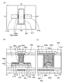
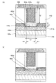
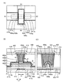
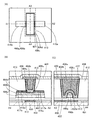
- 4A and 4B are a top view and cross-sectional views illustrating a transistor according to one embodiment of the present invention.
- 4A and 4B are a top view and cross-sectional views illustrating a transistor according to one embodiment of the present invention.
- 4A and 4B are a top view and cross-sectional views illustrating a transistor according to one embodiment of the present invention.
- 4A and 4B are a top view and cross-sectional views illustrating a transistor according to one embodiment of the present invention.
- 4A and 4B are a top view and cross-sectional views illustrating a transistor according to one embodiment of the present invention.
- 4A and 4B are a top view and cross-sectional views illustrating a transistor according to one embodiment of the present invention.
- FIG. 4A and 4B are a top view and cross-sectional views illustrating a transistor according to one embodiment of the present invention.
- 4A and 4B are a top view and cross-sectional views illustrating a transistor according to one embodiment of the present invention.
- FIG. 6 is a cross-sectional view illustrating part of a transistor according to one embodiment of the present invention.
- FIG. 6 is a cross-sectional view illustrating part of a transistor according to one embodiment of the present invention.
- FIG. 6 is a cross-sectional view illustrating part of a transistor according to one embodiment of the present invention.
- 4A and 4B are a top view and cross-sectional views illustrating a transistor according to one embodiment of the present invention.
- FIG. 6 is a cross-sectional view illustrating a transistor according to one embodiment of the present invention.
- 4A and 4B are a top view and cross-sectional views illustrating a transistor according to one embodiment of the present invention.
- 4A and 4B are a top view and cross-sectional views illustrating a transistor according to one embodiment of the present invention.
- 4A and 4B are a top view and cross-sectional views illustrating a transistor according to one embodiment of the present invention.
- 4A and 4B are a top view and cross-sectional views illustrating a transistor according to one embodiment of the present invention.
- 4A and 4B are a top view and cross-sectional views illustrating a transistor according to one embodiment of the present invention.
- FIG. 4A and 4B are a top view and cross-sectional views illustrating a transistor according to one embodiment of the present invention.
- 4A and 4B are a top view and cross-sectional views illustrating a transistor according to one embodiment of the present invention.
- FIG. 6 is a cross-sectional view illustrating part of a transistor according to one embodiment of the present invention.
- FIG. 6 is a cross-sectional view illustrating part of a transistor according to one embodiment of the present invention.
- FIG. 6 is a cross-sectional view illustrating part of a transistor according to one embodiment of the present invention.
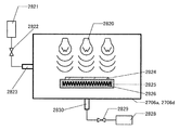
- the top view which shows an example of the film-forming apparatus.
- FIG. 6 illustrates an example of a structure of a film formation apparatus.
- FIG. 6 is a top view illustrating a manufacturing apparatus according to one embodiment of the present invention.
- FIG. 6 is a top view illustrating a chamber according to one embodiment of the present invention.
- FIG. 6 is a top view illustrating a chamber according to one embodiment of the present invention.
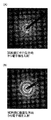
- FIG. 6 is a Cs-corrected high-resolution TEM image in a cross section of a CAAC-OS and a schematic cross-sectional view of the CAAC-OS.
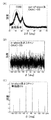
- 6A and 6B illustrate structural analysis by XRD of a CAAC-OS and a single crystal oxide semiconductor.
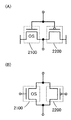
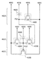
- FIG. 10 is a circuit diagram illustrating a semiconductor device according to one embodiment of the present invention.
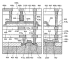
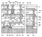
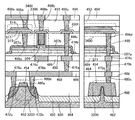
- FIG. 6 is a cross-sectional view illustrating a semiconductor device according to one embodiment of the present invention.
- FIG. 6 is a cross-sectional view illustrating a semiconductor device according to one embodiment of the present invention.
- FIG. 6 is a cross-sectional view illustrating a semiconductor device according to one embodiment of the present invention.
- FIG. 10 is a circuit diagram illustrating a memory device according to one embodiment of the present invention.
- FIG. 6 is a cross-sectional view illustrating a semiconductor device according to one embodiment of the present invention.
- FIG. 6 is a cross-sectional view illustrating a semiconductor device according to one embodiment of the present invention.
- FIG. 6 is a cross-sectional view illustrating a semiconductor device according to one embodiment of the present invention.
- FIG. 10 is a circuit diagram illustrating a semiconductor device according to one embodiment of the present invention.
- FIG. 6 is a cross-sectional view illustrating a semiconductor device according to one embodiment of the present invention.
- FIG. 10 is a circuit diagram illustrating a semiconductor device according to one embodiment of the present invention.
- FIG. 6 is a top view illustrating a semiconductor device according to one embodiment of the present invention.
- 1 is a block diagram illustrating a semiconductor device according to one embodiment of the present invention.
- FIG. 6 is a cross-sectional view illustrating a semiconductor device according to one embodiment of the present invention.
- FIG. 6 is a cross-sectional view illustrating a semiconductor device according to one embodiment of the present invention.
- 4A and 4B are a perspective view and a cross-sectional view illustrating a semiconductor device according to one embodiment of the present invention.
- 1 is a block diagram illustrating a semiconductor device according to one embodiment of the present invention.
- FIG. 10 is a circuit diagram illustrating a semiconductor device according to one embodiment of the present invention.
- 4A and 4B are a circuit diagram, a top view, and a cross-sectional view illustrating a semiconductor device according to one embodiment of the present invention.
- FIG. 6A and 6B are a circuit diagram and a cross-sectional view illustrating a semiconductor device according to one embodiment of the present invention.
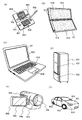
- FIG. 11 is a perspective view illustrating an electronic device according to one embodiment of the present invention.
- 4A and 4B are a top view and cross-sectional views illustrating a transistor according to one embodiment of the present invention.
- the figure explaining a calculation model The figure explaining the low efficiency of a buffer layer, and the interlayer of an electric field strength.
- the shape of an object is defined by “diameter”, “particle diameter”, “size”, “size”, “width”, etc., the length of one side in the smallest cube in which the object fits Alternatively, it may be read as the equivalent circle diameter in one cross section of the object.
- the equivalent circle diameter in one cross section of an object refers to the diameter of a perfect circle having an area equal to that of one cross section of the object.
- a voltage often indicates a potential difference between a certain potential and a reference potential (for example, a ground potential (GND) or a source potential).
- a reference potential for example, a ground potential (GND) or a source potential.
- a voltage can be rephrased as a potential.
- the impurity of the semiconductor means, for example, a component other than the main component constituting the semiconductor.
- an element having a concentration of less than 0.1 atomic% is an impurity.
- impurities for example, semiconductor DOS (Density of State) may be formed, carrier mobility may be reduced, and crystallinity may be reduced.
- examples of impurities that change the characteristics of the semiconductor include Group 1 elements, Group 2 elements, Group 13 elements, Group 14 elements, Group 15 elements, and components other than main components Examples include transition metals, and in particular, hydrogen (also included in water), lithium, sodium, silicon, boron, phosphorus, carbon, nitrogen, and the like.
- oxygen vacancies may be formed by mixing impurities such as hydrogen, for example.
- impurities such as hydrogen, for example.
- examples of impurities that change the characteristics of the semiconductor include group 1 elements, group 2 elements, group 13 elements, and group 15 elements excluding oxygen and hydrogen.
- the channel length refers to, for example, a region where a semiconductor (or a portion where current flows in the semiconductor when the transistor is on) and a gate electrode overlap with each other in a top view of the transistor, or a region where a channel is formed
- the channel length is not necessarily the same in all regions. That is, the channel length of one transistor may not be fixed to one value. Therefore, in this specification, the channel length is any one of values, the maximum value, the minimum value, or the average value in a region where a channel is formed.
- the channel width is, for example, a region in which a semiconductor (or a portion in which a current flows in the semiconductor when the transistor is on) and a gate electrode overlap each other, or a source and a drain in a region where a channel is formed. This is the length of the part. Note that in one transistor, the channel width is not necessarily the same in all regions. That is, the channel width of one transistor may not be fixed to one value. Therefore, in this specification, the channel width is any one of values, the maximum value, the minimum value, or the average value in a region where a channel is formed.
- the channel width in a region where a channel is actually formed (hereinafter referred to as an effective channel width) and the channel width shown in a top view of the transistor (hereinafter, apparent channel width). May be different).
- the effective channel width is larger than the apparent channel width shown in the top view of the transistor, and the influence may not be negligible.
- the ratio of the channel region formed on the side surface of the semiconductor may be large. In that case, the effective channel width in which the channel is actually formed is larger than the apparent channel width shown in the top view.
- an apparent channel width which is a length of a portion where a source and a drain face each other in a region where a semiconductor and a gate electrode overlap with each other in a top view of a transistor is referred to as an “enclosed channel width ( SCW: Surrounded Channel Width).
- SCW Surrounded Channel Width
- channel width in the case where the term “channel width” is simply used, it may denote an enclosed channel width or an apparent channel width.
- channel width in the case where the term “channel width” is simply used, it may denote an effective channel width. Note that the channel length, channel width, effective channel width, apparent channel width, enclosed channel width, and the like can be determined by obtaining a cross-sectional TEM image and analyzing the image. it can.
- the calculation may be performed using the enclosed channel width. In that case, the value may be different from that calculated using the effective channel width.
- A has a shape protruding from B
- at least one end of A has a shape outside of at least one end of B in a top view or a cross-sectional view. May show. Therefore, when it is described that A has a shape protruding from B, for example, in a top view, it can be read that one end of A has a shape outside of one end of B.
- parallel refers to a state in which two straight lines are arranged at an angle of ⁇ 10 ° to 10 °. Therefore, the case of ⁇ 5 ° to 5 ° is also included.
- Very refers to a state in which two straight lines are arranged at an angle of 80 ° to 100 °. Therefore, the case of 85 ° to 95 ° is also included.
- semiconductor can be read as “oxide semiconductor”.
- Semiconductors include group 14 semiconductors such as silicon and germanium, compound semiconductors such as silicon carbide, germanium silicide, gallium arsenide, indium phosphide, zinc selenide, cadmium sulfide, and oxide semiconductors, carbon nanotubes, graphene, and organic A semiconductor or the like can be used.
- a silicon oxynitride film refers to a film having a higher oxygen content than nitrogen as a composition
- a silicon nitride oxide film has a nitrogen content as compared to oxygen as a composition.
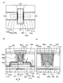
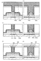
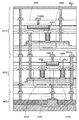
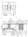
- FIG. 1A, 1B, and 1C are a top view and cross-sectional views of a semiconductor device according to one embodiment of the present invention.
- FIG. 1A is a top view.
- 1B is a cross-sectional view corresponding to the alternate long and short dash line A1-A2 illustrated in FIG. 1A and illustrates a cross-sectional shape in the channel length direction.
- FIG. 1C is a cross-sectional view corresponding to the dashed-dotted line A3-A4 illustrated in FIG. 1A and illustrates a cross-sectional shape in the channel width direction. Note that in the top view of FIG. 1A, some elements are omitted for clarity.
- 1 includes a conductor 413 and an insulator 401 over a substrate 400, an insulator 402 over the conductor 413 and the insulator 401, an insulator 406a over the insulator 402, and a semiconductor over the insulator 406a.
- a conductor 416a and a conductor 416b having a region in contact with the top surface of the semiconductor 406b, a metal oxide 417a and a metal oxide 417b in contact with the conductor 416a and the conductor 416b, respectively, an insulator 402, a metal An insulator 410 in contact with the top surface of the oxide 417a and the top surface of the metal oxide 417b and having an opening; a side surface of the metal oxide 417a; a side surface of the metal oxide 417b; and an insulator 406c in contact with the top surface and side surfaces of the semiconductor 406b.
- the insulator 412 in contact with the side surface of the opening of the insulator 406c and the insulator 410, and the insulator 412 Placed on the semiconductor 406b through a preliminary insulator 406c, having an electrical conductor 404 having a conductor 404a, and conductors 404b, the.
- the conductor 404a faces the side surface of the opening of the insulator 410 with the conductor 404b and the insulator 412 interposed therebetween.
- the conductor 420a and the conductor 420 over the conductor 404b and the insulator 412 and the insulator 408 over the conductor 420 are provided over the transistor.
- the conductor 413 and the insulator 401 are not essential components, and the conductor 413 and the insulator 401 are not provided. It is good also as a structure.
- the insulator 406c preferably includes at least one element other than oxygen included in the semiconductor 406b. Accordingly, generation of defects can be suppressed at the interface between the semiconductor 406b and the insulator 406c. In addition, the crystallinity of the insulator 406c can be improved.
- the semiconductor 406b and the insulator 406c preferably include a CAAC-OS which will be described later.
- the insulator 406a also preferably includes a CAAC-OS.
- the conductors 404a and 404b function as a first gate electrode.
- at least one of the conductors 404a and 404b is preferably a conductor that does not transmit oxygen.
- the insulator 412 functions as a first gate insulator.
- the conductor 413 functions as a second gate electrode.
- the conductor 413 can have a stacked structure including a conductor that does not transmit oxygen. With a stacked structure including a conductor that does not allow oxygen to pass therethrough, reduction in conductivity due to oxidation of the conductor 413 can be prevented.
- the insulator 402 functions as a second gate insulator. The threshold voltage of the transistor can be controlled by the potential applied to the conductor 413.
- a current (ON current) at the time of conduction can be increased. Note that the function of the first gate electrode and the function of the second gate electrode may be interchanged.
- the conductor 416a functions as one of a source electrode and a drain electrode.
- the conductor 416b functions as the other of the source electrode and the drain electrode. Note that the conductivity of the conductor can be measured using a two-terminal method or the like.
- the metal oxide 417a and the metal oxide 417b have a function of reducing electric field concentration generated in the end portion of the conductor 416a or the conductor 416b.
- the metal oxide 417a and the metal oxide 417b each preferably have a region with a different thickness.
- the thicknesses of the metal oxide 417a and the metal oxide 417b in contact with the side surface of the conductor 416a or the conductor 416b in the side surface direction are the metal oxide 417a and the metal oxide 417b in contact with the upper surface of the conductor 416a or the conductor 416b. It is preferable that the thickness is larger than the thickness in the upper surface direction. That is, it is preferable that the metal oxide 417a and the metal oxide 417b have a large thickness in a region in contact with the insulator 406c or the insulator 412.
- end portions of the metal oxide 417 a and the metal oxide 417 b preferably have a region overlapping with the opening of the insulator 410. That is, since the metal oxide 417a and the metal oxide 417b have a region overlapping with the insulator 412, electric field concentration can be effectively reduced and reliability can be improved. Moreover, the short channel effect can be suppressed. Further, leakage current generated between the conductor 416a and the conductor 404 can be suppressed.
- the resistance of the semiconductor 406b can be controlled by a potential applied to the conductor 404. That is, conduction / non-conduction between the conductors 416a can be controlled by a potential applied to the conductor 404.
- the upper surface of the semiconductor 406b is in contact with the conductor 416a.
- the semiconductor 406b can be electrically surrounded by an electric field of the conductor 404 functioning as a gate electrode.
- a structure of a transistor that electrically surrounds a semiconductor by an electric field of a gate electrode is referred to as a surrounded channel (s-channel) structure. Therefore, a channel may be formed in the entire semiconductor 406b.
- s-channel structure a large current can flow between the source and the drain of the transistor, and a current (on-state current) during conduction can be increased.
- the semiconductor 406b is surrounded by the electric field of the conductor 404, current during off-state (off-state current) can be reduced.
- a region functioning as a gate electrode is formed in a self-aligned manner so as to fill an opening formed by the insulator 410 or the like. Therefore, a TGSAs-channel FET (Trench Gate Self) is formed. It can also be called Align s-channel FET).
- a length between the top surface of the semiconductor 406b and the bottom surface of the conductor 404 in a region overlapping with the conductor 404 is t1.
- a length between a region in contact with the bottom surface of the metal oxide 417a and a region in contact with the bottom surface of the conductor 404 in the semiconductor 406b is L1.
- a length between a region in contact with the bottom surface of the metal oxide 417b and a region between the region in contact with the bottom surface of the conductor 404 is L1.
- the region having the length L1 can reduce the off-state current of the transistor. On the other hand, when the region is too large, the on-state current of the transistor is decreased.
- an element other than oxygen (hydrogen, silicon, or the like) included in the adjacent insulator does not enter the region where the channel is formed. Can be blocked. Accordingly, the insulator 406c only needs to be formed over at least the semiconductor 406b.
- the insulator 406c is not provided on the side surface of the conductor 404 with the insulator 412 interposed therebetween, or the region where the insulator 406c covers the side surface of the conductor 404 with the insulator 412 is provided
- the formed L1 can be reduced. Therefore, t1 is larger than L1, and L1 / t1 is less than 1.
- a length between the conductor 416a or 416b and the conductor 420 is t2.
- the length between the metal oxide 417a and the metal oxide 417b is L2.
- a parasitic capacitance may be formed between the conductor 420 and the conductor 416a or the conductor 416b.
- a time required for charging the parasitic capacitance is required in the transistor operation, and the response of the transistor and thus the response of the semiconductor device are deteriorated.
- t2 is preferably long enough that the parasitic capacitance is negligible compared to the gate capacitance.
- t2 may be larger than L2, and t2 / L2 is preferably 1.5 or more and 2 or less.
- an insulator substrate, a semiconductor substrate, or a conductor substrate may be used.
- the insulator substrate include a glass substrate, a quartz substrate, a sapphire substrate, a stabilized zirconia substrate (such as a yttria stabilized zirconia substrate), and a resin substrate.
- the semiconductor substrate include a single semiconductor substrate such as silicon or germanium, or a compound semiconductor substrate made of silicon carbide, silicon germanium, gallium arsenide, indium phosphide, zinc oxide, or gallium oxide.
- there is a semiconductor substrate having an insulator region inside the semiconductor substrate for example, an SOI (Silicon On Insulator) substrate.
- the conductor substrate examples include a graphite substrate, a metal substrate, an alloy substrate, and a conductive resin substrate.
- a substrate having a metal nitride examples include a substrate having a metal oxide, and the like.
- a substrate in which a conductor or a semiconductor is provided on an insulator substrate examples include a substrate in which a conductor or an insulator is provided on a semiconductor substrate, a substrate in which a semiconductor or an insulator is provided on a conductor substrate, and the like.
- a substrate in which an element is provided may be used.
- the element provided on the substrate include a capacitor element, a resistor element, a switch element, a light emitting element, and a memory element.
- a flexible substrate may be used as the substrate 400.
- a method for providing a transistor over a flexible substrate there is a method in which after a transistor is manufactured over a non-flexible substrate, the transistor is peeled off and transferred to the substrate 400 which is a flexible substrate.
- a separation layer is preferably provided between the non-flexible substrate and the transistor.
- a sheet, a film, a foil, or the like in which fibers are knitted may be used as the substrate 400.
- the substrate 400 may have elasticity. Further, the substrate 400 may have a property of returning to the original shape when bending or pulling is stopped. Or you may have a property which does not return to an original shape.
- the substrate 400 has a region having a thickness of, for example, 5 ⁇ m to 700 ⁇ m, preferably 10 ⁇ m to 500 ⁇ m, and more preferably 15 ⁇ m to 300 ⁇ m.
- a semiconductor device including a transistor can be reduced in weight.
- the substrate 400 may have elasticity even when glass or the like is used, or may have a property of returning to its original shape when bending or pulling is stopped. Therefore, an impact applied to the semiconductor device on the substrate 400 due to a drop or the like can be reduced. That is, a durable semiconductor device can be provided.
- the substrate 400 which is a flexible substrate
- a metal, an alloy, a resin, glass, or fiber thereof can be used as the substrate 400 which is a flexible substrate.
- the substrate 400, which is a flexible substrate is preferable because the deformation due to the environment is suppressed as the linear expansion coefficient is lower.
- a material having a linear expansion coefficient of 1 ⁇ 10 ⁇ 3 / K or less, 5 ⁇ 10 ⁇ 5 / K or less, or 1 ⁇ 10 ⁇ 5 / K or less is used as the substrate 400 that is a flexible substrate.
- the resin include polyester, polyolefin, polyamide (such as nylon and aramid), polyimide, polycarbonate, and acrylic.
- aramid has a low coefficient of linear expansion, it is suitable as the substrate 400 that is a flexible substrate.
- an insulator having a function of blocking impurities such as hydrogen and oxygen By surrounding the transistor with an insulator having a function of blocking impurities such as hydrogen and oxygen, electrical characteristics of the transistor can be stabilized.
- an insulator having a function of blocking impurities such as hydrogen and oxygen may be used as the insulator 408 as the insulator 408, an insulator having a function of blocking impurities such as hydrogen and oxygen may be used as the insulator 408
- Examples of the insulator having a function of blocking impurities such as hydrogen and oxygen include boron, carbon, nitrogen, oxygen, fluorine, magnesium, aluminum, silicon, phosphorus, chlorine, argon, gallium, germanium, yttrium, zirconium, and lanthanum.
- An insulator containing neodymium, hafnium, or tantalum may be used as a single layer or a stacked layer.
- the insulator 408 aluminum oxide, magnesium oxide, silicon nitride oxide, silicon nitride, gallium oxide, germanium oxide, yttrium oxide, zirconium oxide, lanthanum oxide, neodymium oxide, hafnium oxide, or tantalum oxide may be used. .
- the insulator 408 preferably includes aluminum oxide.
- oxygen can be added to the insulator 410 which serves as a base layer of the insulator 408.
- oxygen can be added to the side surface of the insulator 412. The added oxygen becomes excess oxygen in the insulator 410 or the insulator 412.
- the insulator 408 includes aluminum oxide, entry of impurities such as hydrogen into the semiconductor 406b can be suppressed.
- the insulator 408 includes aluminum oxide, outward diffusion of excess oxygen added to the insulator 410 and the insulator 412 can be reduced.
- the insulator 402 for example, an insulator containing boron, carbon, nitrogen, oxygen, fluorine, magnesium, aluminum, silicon, phosphorus, chlorine, argon, gallium, germanium, yttrium, zirconium, lanthanum, neodymium, hafnium, or tantalum is used. Or a single layer or a stacked layer.
- the insulator 402 preferably includes silicon oxide or silicon oxynitride.
- the insulator 410 preferably includes an insulator having a low relative dielectric constant.
- the insulator 410 includes silicon oxide, silicon oxynitride, silicon nitride oxide, silicon nitride, silicon oxide to which fluorine is added, silicon oxide to which carbon is added, silicon oxide to which carbon and nitrogen are added, and silicon oxide having a hole Or it is preferable to have resin etc.
- the insulator 410 is formed using silicon oxide, silicon oxynitride, silicon nitride oxide, silicon nitride, silicon oxide to which fluorine is added, silicon oxide to which carbon is added, silicon oxide to which carbon and nitrogen are added, or silicon oxide having a hole And a laminated structure of resin.
- silicon oxide and silicon oxynitride are thermally stable, a laminated structure having a low thermal stability and a low relative dielectric constant can be obtained by combining with silicon.
- the resin include polyester, polyolefin, polyamide (such as nylon and aramid), polyimide, polycarbonate, and acrylic.
- the insulator 412 for example, an insulator containing boron, carbon, nitrogen, oxygen, fluorine, magnesium, aluminum, silicon, phosphorus, chlorine, argon, gallium, germanium, yttrium, zirconium, lanthanum, neodymium, hafnium, or tantalum is used. Or a single layer or a stacked layer.
- the insulator 412 preferably includes silicon oxide or silicon oxynitride.
- the insulator 412 preferably includes an insulator having a high relative dielectric constant.
- the insulator 412 includes gallium oxide, hafnium oxide, an oxide including aluminum and hafnium, an oxynitride including aluminum and hafnium, an oxide including silicon and hafnium, or an oxynitride including silicon and hafnium. It is preferable.
- the insulator 412 preferably has a stacked structure of silicon oxide or silicon oxynitride and an insulator with a high relative dielectric constant. Since silicon oxide and silicon oxynitride are thermally stable, a stacked structure having high thermal stability and high relative dielectric constant can be obtained by combining with an insulator having high relative dielectric constant.
- a trap center may be formed at the interface between aluminum oxide, gallium oxide, or hafnium oxide and silicon oxide or silicon oxynitride. is there. In some cases, the trap center can change the threshold voltage of the transistor in the positive direction by capturing electrons.
- Examples of the conductor 416a and the conductor 416b include boron, nitrogen, oxygen, fluorine, silicon, phosphorus, aluminum, titanium, chromium, manganese, cobalt, nickel, copper, zinc, gallium, yttrium, zirconium, molybdenum, ruthenium,
- a conductor including one or more of platinum, silver, indium, tin, tantalum, and tungsten may be used as a single layer or a stacked layer.
- an alloy film or a compound film may be used.
- a conductor containing aluminum, a conductor containing copper and titanium, a conductor containing copper and manganese, a conductor containing indium, tin and oxygen, or titanium and nitrogen A conductive material or the like may be used.
- Examples of the metal oxide 417a and the metal oxide 417b include aluminum, titanium, chromium, manganese, cobalt, nickel, copper, zinc, gallium, yttrium, zirconium, molybdenum, ruthenium, platinum, silver, indium, tin, tantalum, and the like.
- a metal oxide containing at least one tungsten may be used. In particular, tungsten oxide is preferable.
- Examples of the conductor 404, the conductor 413, and the conductor 420 include boron, nitrogen, oxygen, fluorine, silicon, phosphorus, aluminum, titanium, chromium, manganese, cobalt, nickel, copper, zinc, gallium, yttrium, and zirconium.
- a conductor containing one or more of molybdenum, ruthenium, silver, indium, tin, tantalum, and tungsten may be used as a single layer or a stacked layer.
- an alloy film or a compound film may be used.
- a conductor containing aluminum, a conductor containing copper and titanium, a conductor containing copper and manganese, a conductor containing indium, tin and oxygen, or titanium and nitrogen A conductive material or the like may be used.
- An oxide semiconductor is preferably used as the semiconductor 406b.
- silicon including strained silicon
- germanium silicon germanium, silicon carbide, gallium arsenide, aluminum gallium arsenide, indium phosphide, gallium nitride, an organic semiconductor, or the like may be used.
- an oxide including one or more elements other than oxygen included in the semiconductor 406b or two or more elements is preferably used.
- silicon including strained silicon
- germanium, silicon germanium, silicon carbide, gallium arsenide, aluminum gallium arsenide, indium phosphide, gallium nitride, an organic semiconductor, or the like may be used.
- the semiconductor 406b is an oxide semiconductor containing indium, for example.
- the carrier mobility electron mobility
- the semiconductor 406b preferably contains an element M.
- the element M is preferably aluminum, gallium, yttrium, tin, or the like.
- Other elements applicable to the element M include boron, silicon, titanium, iron, nickel, germanium, yttrium, zirconium, molybdenum, lanthanum, cerium, neodymium, hafnium, tantalum, magnesium, tungsten, and the like.
- the element M may be a combination of a plurality of the aforementioned elements.
- the element M is an element having a high binding energy with oxygen, for example.
- the element M is an element having a function of increasing the energy gap of the oxide semiconductor, for example.
- the semiconductor 406b preferably contains zinc. An oxide semiconductor may be easily crystallized when it contains zinc.
- the semiconductor 406b is not limited to the oxide semiconductor containing indium.
- the semiconductor 406b may be an oxide semiconductor containing zinc, an oxide semiconductor containing gallium, an oxide semiconductor containing tin, or the like that does not contain indium, such as zinc tin oxide and gallium tin oxide.
- an oxide with a wide energy gap is used, for example.
- the energy gap of the semiconductor 406b is, for example, 2.5 eV to 4.2 eV, preferably 2.8 eV to 3.8 eV, and more preferably 3 eV to 3.5 eV.
- the insulators 406a and 406c are oxides composed of one or more elements other than oxygen included in the semiconductor 406b or two or more elements. Since the insulator 406a and the insulator 406c are composed of one or more elements other than oxygen constituting the semiconductor 406b, or two or more elements, the interface between the insulator 406a and the semiconductor 406b and the interface between the semiconductor 406b and the insulator 406c , Defect levels are difficult to form.
- the semiconductor 406b an oxide having an electron affinity higher than those of the insulators 406a and 406c is used.
- the semiconductor 406b has an oxide affinity higher than that of the insulators 406a and 406c by 0.07 eV to 1.3 eV, preferably 0.1 eV to 0.7 eV, more preferably 0.15 eV to 0.4 eV.
- the electron affinity is an energy difference between the vacuum level and the lower end of the conduction band.
- the mixed region there is a mixed region of the insulator 406a and the semiconductor 406b between the insulator 406a and the semiconductor 406b. Further, in some cases, there is a mixed region of the semiconductor 406b and the insulator 406c between the semiconductor 406b and the insulator 406c.
- the mixed region has a low density of defect states. Therefore, energy of the stacked body of the insulator 406a, the semiconductor 406b, and the insulator 406c changes continuously in the vicinity of each interface (also referred to as continuous bonding). Note that there are cases in which the interfaces of the insulator 406a, the semiconductor 406b, and the insulator 406c cannot be clearly distinguished.
- the on-state current of the transistor can be increased as the factor that hinders the movement of electrons is reduced. Electron movement is inhibited, for example, even when the physical unevenness of the channel formation region is large.
- the average surface roughness (also referred to as Ra) in the range of 1 ⁇ m ⁇ 1 ⁇ m is less than 1 nm, preferably less than 0.6 nm, more preferably less than 0.5 nm, and more preferably less than 0.4 nm.
- the maximum height difference (also referred to as PV) in the range of 1 ⁇ m ⁇ 1 ⁇ m is less than 10 nm, preferably less than 9 nm, more preferably less than 8 nm, and more preferably less than 7 nm.
- the RMS roughness, Ra, and PV can be measured using a scanning probe microscope system SPA-500 manufactured by SII Nano Technology.
- the above three-layer structure is an example.
- a stacked structure including one or more of the insulators exemplified as the insulator 406a and the insulator 406c above or below the insulator 406a or above or below the insulator 406c may be employed.
- the substrate 400 is prepared.
- an insulator to be the insulator 401 is formed over the substrate 400, an opening is formed in the insulator 401, and the insulator 401 is electrically conductive.
- a conductive film to be the body 413 is formed.
- the conductor to be the conductor 413 can be formed by a sputtering method, a CVD method, an MBE method, a PLD method, an ALD method, or the like.
- the conductor 413 may have a multilayer structure including a conductor that does not allow oxygen to pass therethrough.
- the conductor 413 may be embedded in the opening portion of the insulator 402 by using chemical mechanical polishing (CMP) or the like.
- CMP chemical mechanical polishing
- the conductor 413 may be formed by forming a conductor and processing it using a photolithography method or the like.
- a resist is exposed through a mask.
- a resist mask is formed by removing or leaving the exposed region using a developer.
- a conductor, a semiconductor, an insulator, or the like can be processed into a desired shape by etching through the resist mask.
- the resist mask may be formed by exposing the resist using KrF excimer laser light, ArF excimer laser light, EUV (Extreme Ultraviolet) light, or the like.
- an immersion technique may be used in which exposure is performed by filling a liquid (for example, water) between the substrate and the projection lens.
- an electron beam or an ion beam may be used.
- a mask is not necessary when an electron beam or an ion beam is used.
- the resist mask is removed by performing a dry etching process such as ashing, performing a wet etching process, performing a wet etching process in addition to the dry etching process, or performing a dry etching process in addition to the wet etching process. be able to.
- a capacitively coupled plasma (CCP) etching apparatus having parallel plate electrodes can be used as the dry etching apparatus.
- the capacitively coupled plasma etching apparatus having parallel plate electrodes may be configured to apply a high frequency power source to one of the parallel plate electrodes.
- a configuration in which a plurality of different high-frequency power sources are applied to one electrode of the parallel plate electrode may be employed.
- mold electrode may be sufficient.
- mold electrode may be sufficient.
- a dry etching apparatus having a high-density plasma source can be used.
- an inductively coupled plasma (ICP) etching apparatus can be used as the dry etching apparatus having a high-density plasma source.
- high-density plasma treatment may be performed.
- the high-density plasma treatment is preferably performed in an oxygen atmosphere or a nitrogen atmosphere.
- An oxygen atmosphere is a gas atmosphere having oxygen atoms, such as oxygen, ozone, or nitrogen oxide (nitrogen monoxide, nitrogen dioxide, dinitrogen monoxide, dinitrogen trioxide, dinitrogen tetroxide, dinitrogen pentoxide, etc.) Say the atmosphere.
- an inert gas such as nitrogen or a rare gas (such as helium or argon) may be included.
- the high-density plasma treatment in a nitrogen atmosphere for example, the high-density plasma treatment is performed in an atmosphere containing nitrogen and a rare gas, an atmosphere containing nitrogen, hydrogen, and a rare gas, or an atmosphere containing ammonia and a rare gas. Just do it.
- the surface of the object to be processed and the vicinity thereof can be nitrided.
- the region to be nitrided can be formed extremely thin on the surface side of the object to be processed. Further, impurity diffusion can be suppressed by the nitrided region.
- the high-density plasma treatment may be performed in an oxygen atmosphere and then in a nitrogen atmosphere, or may be performed in a nitrogen atmosphere and then in an oxygen atmosphere. Further, annealing treatment may be performed before and after each high-density plasma treatment.
- a high-frequency generator having a frequency of 0.3 GHz to 3.0 GHz, 0.7 GHz to 1.1 GHz, or 2.2 GHz to 2.8 GHz (typically 2.45 GHz) is used.
- a microwave generated using the above may be used.
- the processing pressure is 10 Pa to 5000 Pa, preferably 200 Pa to 1500 Pa, more preferably 300 Pa to 1000 Pa, the substrate temperature is 100 ° C. to 600 ° C. (typically 400 ° C.), and oxygen and argon are mixed. It can be performed using gas.
- the high-density plasma is generated by using a microwave of 2.45 GHz, for example, and has an electron density of 1 ⁇ 10 11 / cm 3 or more and 1 ⁇ 10 13 / cm 3 or less, an electron temperature of 2 eV or less, or an ion energy of 5 eV or less. Is preferable.
- Such high-density plasma treatment has low radical kinetic energy, and is less damaged by plasma than conventional plasma treatment. Therefore, a film with few defects can be formed.
- the distance from the antenna that generates the microwave to the object to be processed is 5 mm to 120 mm, preferably 20 mm to 60 mm.
- a plasma power source that applies an RF (Radio Frequency) bias to the substrate side may be provided.
- RF Radio Frequency
- 13.56 MHz or 27.12 MHz may be used as the frequency of the RF bias.
- High-density oxygen ions can be generated by using high-density plasma, and by applying an RF bias to the substrate side, oxygen ions generated by the high-density plasma can be efficiently guided to the object to be processed. Therefore, it is preferable to perform high-density plasma treatment while applying a substrate bias.
- the annealing treatment may be continuously performed without being exposed to the atmosphere. Further, the high-density plasma treatment may be continuously performed after the annealing treatment without being exposed to the atmosphere. By continuously performing the high-density plasma treatment and the annealing treatment, it is possible to prevent impurities from being mixed between the treatments. In addition, by performing an annealing treatment after performing a high-density plasma treatment in an oxygen atmosphere, it is possible to desorb unnecessary oxygen that has not been used for oxygen deficiency compensation among oxygen added to the object to be treated. it can.
- the annealing process may be performed by lamp annealing, for example.
- the treatment time for the high-density plasma treatment is preferably 30 seconds to 120 minutes, 1 minute to 90 minutes, 2 minutes to 30 minutes, or 3 minutes to 15 minutes.
- the annealing treatment is performed at 250 ° C. or higher and 800 ° C. or lower, 300 ° C. or higher and 700 ° C. or lower, or 400 ° C. or higher and 600 ° C. or lower.
- the processing time is 30 seconds or longer and 120 minutes or shorter, 1 minute or longer and 90 minutes or shorter, Or less, or 3 minutes or more and 15 minutes or less.
- the insulator 402 is formed by a sputtering method, a chemical vapor deposition (CVD) method, a molecular beam epitaxy (MBE) method or a pulse laser deposition (PLD: Pulsed Laser Deposition) method, an atomic layer.
- the deposition can be performed using an ALD (Atomic Layer Deposition) method or the like.
- the CVD method can be classified into a plasma CVD (PECVD: Plasma Enhanced CVD) method using plasma, a thermal CVD (TCVD: Thermal CVD) method using heat, a photo CVD (Photo CVD) method using light, and the like.
- PECVD Plasma Enhanced CVD
- TCVD Thermal CVD
- Photo CVD Photo CVD
- MCVD Metal CVD
- MOCVD Metal Organic CVD
- the thermal CVD method is a film formation method that can reduce plasma damage to an object to be processed because plasma is not used.
- a wiring, an electrode, an element (a transistor, a capacitor, or the like) included in the semiconductor device may be charged up by receiving electric charge from plasma.
- a wiring, an electrode, an element, or the like included in the semiconductor device may be destroyed by the accumulated charge.
- damage due to exposure to plasma does not occur as described above, so that the yield of semiconductor devices can be increased.
- the thermal CVD method is not exposed to plasma during film formation, a film with few defects is easily obtained.
- the ALD method is also a film forming method that can reduce plasma damage to an object to be processed.
- the ALD method does not cause plasma damage during film formation, a film with few defects can be obtained.
- the CVD method and the ALD method are film forming methods in which a film is formed by a reaction on the surface of an object to be processed, unlike a film forming method in which particles emitted from a target or the like are deposited. Therefore, it is a film forming method that is not easily affected by the shape of the object to be processed and has good step coverage.
- the ALD method has excellent step coverage and excellent thickness uniformity, and thus is suitable for covering the surface of an opening having a high aspect ratio.
- the ALD method since the ALD method has a low film formation rate, it may be preferable to use it in combination with another film formation method such as a CVD method with a high film formation rate.
- the composition of the obtained film can be controlled by the flow rate ratio of the source gases.
- a film having an arbitrary composition can be formed depending on the flow rate ratio of the source gases.
- a film whose composition is continuously changed can be formed by changing the flow rate ratio of the source gas while forming the film.
- carbon, hydrogen, or the like may be desorbed by performing the above-described high-density plasma treatment.
- high-density plasma treatment by performing high-density plasma treatment in an oxygen atmosphere, organic compounds such as hydrocarbons can be detached from the object to be processed.
- treatment for adding oxygen to the insulator 402 may be performed.
- the treatment for adding oxygen include an ion implantation method and a plasma treatment method. Note that oxygen added to the insulator 402 becomes excess oxygen.
- an insulator to be the insulator 406a and a semiconductor to be the semiconductor 406b are formed.
- an insulator to be the insulator 406a is formed over the insulator 402.
- the insulator to be the insulator 406a can be formed by a sputtering method, a CVD method, an MBE method, a PLD method, an ALD method, or the like.
- a film formation method using an opposing target sputtering apparatus can also be referred to as a VDSP (vapor deposition SP).
- an insulator By forming an insulator using an opposed target sputtering apparatus, plasma damage during film formation can be reduced. Therefore, oxygen vacancies in the film can be reduced. In addition, by using an opposed target sputtering apparatus, film formation at high vacuum is possible. Accordingly, the impurity concentration (eg, hydrogen, rare gas (such as argon), water, or the like) in the formed insulator can be reduced.
- the impurity concentration eg, hydrogen, rare gas (such as argon), water, or the like
- a sputtering apparatus having an inductively coupled antenna conductor plate may be used. Accordingly, a film having a high film formation rate and a large area and high uniformity can be formed.
- the film formation is preferably performed using a gas containing oxygen, a rare gas, a gas containing nitrogen, or the like.
- a gas containing nitrogen for example, nitrogen (N 2 ), dinitrogen monoxide (N 2 O), ammonia (NH 3 ), or the like may be used.
- carbon, hydrogen, or the like may be desorbed by performing the above-described high-density plasma treatment.
- high-density plasma treatment by performing high-density plasma treatment in an oxygen atmosphere, organic compounds such as hydrocarbons can be detached from the object to be processed.
- treatment for adding oxygen to the insulator to be the insulator 406a may be performed.
- the treatment for adding oxygen include an ion implantation method and a plasma treatment method. Note that oxygen added to the insulator to be the insulator 406a becomes excess oxygen.
- a semiconductor to be the semiconductor 406b is formed over the insulator to be the insulator 406a.
- the semiconductor can be formed by a sputtering method, a CVD method, an MBE method, a PLD method, an ALD method, or the like. In particular, it is preferable to form a film using an opposed target sputtering apparatus.
- the impurity concentration eg, hydrogen, rare gas (such as argon), water, or the like
- the impurity concentration eg, hydrogen, rare gas (such as argon), water, or the like
- a sputtering apparatus having an inductively coupled antenna conductor plate may be used. Accordingly, a film having a high film formation rate and a large area and high uniformity can be formed.
- the film formation is preferably performed using a gas containing oxygen, a rare gas, a gas containing nitrogen, or the like.
- a gas containing nitrogen for example, nitrogen (N 2 ), dinitrogen monoxide (N 2 O), ammonia (NH 3 ), or the like may be used.
- the first heat treatment may be performed at 250 ° C to 650 ° C, preferably 450 ° C to 600 ° C.
- the first heat treatment is performed in an inert gas atmosphere or an atmosphere containing an oxidizing gas at 10 ppm or more, 1% or more, or 10% or more.
- the first heat treatment may be performed in a reduced pressure state.
- the first heat treatment may be performed in an atmosphere containing an oxidizing gas of 10 ppm or more, 1% or more, or 10% or more to supplement the desorbed oxygen after the heat treatment in an inert gas atmosphere. Good.
- the crystallinity of the semiconductor can be increased, impurities such as hydrogen and water can be removed, and the like.
- plasma treatment including oxygen may be performed in a reduced pressure state.
- the plasma treatment including oxygen it is preferable to use an apparatus having a power source that generates high-density plasma using microwaves, for example.
- a plasma power source that applies RF (Radio Frequency) may be provided on the substrate side.
- High density oxygen radicals can be generated by using high density plasma, and by applying RF to the substrate side, oxygen radicals generated by the high density plasma can be efficiently introduced into the semiconductor 406b.
- plasma treatment containing oxygen may be performed to supplement oxygen that has been desorbed after performing plasma treatment containing an inert gas using this apparatus.
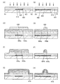
- the insulator to be the insulator 406a and the semiconductor to be the semiconductor 406b are processed by a photolithography method or the like using the resist mask 430, so that the insulator A multilayer film including 406a and the semiconductor 406b is formed (see FIG. 9C).
- the insulator 402 is also etched, and part of the region may be thinned. That is, the insulator 402 may have a shape having a protrusion in a region in contact with the multilayer film.
- carbon, hydrogen, or the like may be desorbed by performing the above-described high-density plasma treatment.
- high-density plasma treatment by performing high-density plasma treatment in an oxygen atmosphere, organic compounds such as hydrocarbons can be detached from the object to be processed.
- a conductor 416 is formed.
- the conductor 416 is formed.
- the conductor 416 can be formed by a sputtering method, a CVD method, an MBE method, a PLD method, an ALD method, or the like.
- the conductor 416 has a shape covering the multilayer film.
- a side surface of the insulator 406a, a top surface of the semiconductor 406b, and a part of a side surface of the semiconductor 406b may be damaged, so that a region with reduced resistance may be formed.
- part of the insulator 406a and the semiconductor 406b includes regions with reduced resistance, the contact resistance between the conductor 416 and the semiconductor 406b can be reduced.
- carbon, hydrogen, or the like may be desorbed by performing the above-described high-density plasma treatment.
- high-density plasma treatment by performing high-density plasma treatment in an oxygen atmosphere, organic compounds such as hydrocarbons can be detached from the object to be processed.
- the conductor 416a and the conductor 416b are formed by processing using a photolithography method or the like.
- carbon, hydrogen, or the like may be desorbed by performing the above-described high-density plasma treatment.
- high-density plasma treatment by performing high-density plasma treatment in an oxygen atmosphere, organic compounds such as hydrocarbons can be detached from the object to be processed.
- an insulator to be the insulator 410 is formed.
- the insulator to be the insulator 410 can be formed by a sputtering method, a CVD method, an MBE method, a PLD method, an ALD method, or the like.
- a spin coating method, a dip method, a droplet discharge method (such as an ink jet method), a printing method (such as screen printing or offset printing), a doctor knife method, a roll coater method, or a curtain coater method can be used.
- the insulator to be the insulator 410 may be formed so that the upper surface has flatness.
- the insulator to be the insulator 410 may have a flat upper surface immediately after film formation.
- the insulator to be the insulator 410 may have flatness by removing the insulator and the like from the upper surface so as to be parallel to a reference surface such as the back surface of the substrate after film formation. Such a process is called a flattening process.
- Examples of the planarization treatment include chemical mechanical polishing treatment and dry etching treatment. Note that the top surface of the insulator to be the insulator 410 does not have to have flatness.
- the surface of the conductor 416 is oxidized by oxygen in the deposition gas, and a metal oxide 417 is formed on the upper surface of the conductor 416. That is, since the conductor 416 is an oxide, the thickness of the conductor 416 is reduced.
- carbon, hydrogen, or the like may be desorbed by performing the above-described high-density plasma treatment.
- high-density plasma treatment by performing high-density plasma treatment in an oxygen atmosphere, organic compounds such as hydrocarbons can be detached from the object to be processed.
- a resist mask 431 is formed over the insulator to be the insulator 410 by a lithography method or the like.
- an organic coating film may be provided between the insulator serving as the insulator 410 and the resist mask.
- openings are formed in the insulator 410 and the conductor 416.
- the first process is performed on the insulator to be the insulator 410 until it reaches the upper surface of the conductor 416 by using a dry etching method or the like.
- a dry etching apparatus described above can be used for the dry etching method, it is preferable to use a dry etching apparatus having a configuration in which high-frequency power sources having different frequencies are connected to the parallel plate electrodes.
- the conductor 416 is subjected to second processing using a dry etching method or the like, so that the conductor 416 is separated into a conductor 416a and a conductor 416b.
- the processing of the insulator 410 and the processing of the conductor 416 may be performed in a common photolithography process. The number of processes can be reduced by sharing the process by the photolithography method. Therefore, productivity of a semiconductor device including a transistor can be increased.
- the semiconductor 406b has an exposed region. Part of the exposed region of the semiconductor 406b may be removed by the second process described above. Further, an impurity element such as a residual component of an etching gas may adhere to the exposed semiconductor 406b. For example, when a chlorine-based gas is used as an etching gas, chlorine or the like may adhere. In addition, when a hydrocarbon-based gas is used as an etching gas, carbon or hydrogen may adhere. Therefore, it is preferable to reduce impurity elements attached to the exposed surface of the semiconductor 406b. The reduction of the impurities may be performed by, for example, a cleaning process using dilute hydrofluoric acid, a cleaning process using ozone, or a cleaning process using ultraviolet rays. A plurality of cleaning processes may be combined. Thus, the exposed surface of the semiconductor 406b, in other words, the region where the channel is formed has high resistance.
- an impurity element such as a residual component of an etching gas may adhere to the exposed semiconductor 406b.
- carbon, hydrogen, or the like may be desorbed by performing the above-described high-density plasma treatment.
- high-density plasma treatment by performing high-density plasma treatment in an oxygen atmosphere, organic compounds such as hydrocarbons can be detached from the object to be processed.
- high-density plasma treatment in an oxygen atmosphere, the side surfaces exposed inside the openings of the conductors 416a and 416b are oxidized, and a metal oxide is formed on the side surfaces of the conductors 416a and 416b. Can do.
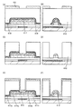
- the insulator 406c is formed over the top surface of the body 410, the insulator 412 is formed.
- the insulator 406c can be formed by a sputtering method.
- a sputtering apparatus used for forming the insulator 406c is described with reference to FIGS.
- FIG. 12 is a cross-sectional view showing a part of the sputtering apparatus 101.
- 12 includes a member 190, a collimator 150 disposed on the member 190, a target holder 120, a backing plate 110 disposed on the target holder 120, and a backing plate 110.
- the target 100 includes a magnet unit 130 including a magnet 130N and a magnet 130S disposed under the target 100 via a backing plate 110, and a magnet holder 132 that supports the magnet unit 130.
- a combination of a plurality of magnets (magnets) is called a magnet unit.
- the magnet unit can be called a cathode, a cathode magnet, a magnetic member, a magnetic component, or the like.
- a substrate stage 170 disposed to face the target 100 and a substrate 160 supported by the substrate stage 170 are also shown.
- magnetic lines of force 180a and magnetic lines of force 180b formed by the magnet unit 130 are shown.
- the target holder 120 and the backing plate 110 are fixed using screws (bolts or the like) and are equipotential. Further, the target holder 120 has a function of supporting the target 100 via the backing plate 110.
- the backing plate 110 has a function of fixing the target 100.
- the sputtering apparatus 101 may have a water channel inside or below the backing plate 110. Then, by causing a fluid (air, nitrogen, rare gas, water, oil, etc.) to flow through the water channel, discharge abnormality due to a rise in the temperature of the target 100 during sputtering, damage to the sputtering apparatus 101 due to deformation of members such as the target 100, and the like. Can be suppressed. At this time, it is preferable that the backing plate 110 and the target 100 are brought into close contact with each other through a bonding material because cooling performance is improved.
- a fluid air, nitrogen, rare gas, water, oil, etc.
- the magnet 130N and the magnet 130S are magnets arranged with different polarities toward the target 100 side.
- the magnet 130N is arranged so that the target 100 side has an N pole
- the magnet 130S is arranged so that the target 100 side has an S pole.
- the arrangement of magnets and polarities in the magnet unit 130 is not limited to the arrangement shown in FIG.
- the magnetic force line 180 a is one of magnetic force lines that form a horizontal magnetic field near the surface of the target 100.
- the vicinity of the surface of the target 100 is, for example, a region having a vertical distance from the target 100 of 0 mm to 10 mm, particularly 0 mm to 5 mm.
- the magnetic force line 180b is one of magnetic force lines that form a horizontal magnetic field at a vertical distance d from the surface of the magnet unit 130.
- the vertical distance d is, for example, 0 mm or more and 20 mm or less, or 5 mm or more and 15 mm or less.
- the potential V1 applied to the target holder 120 is lower than the potential V2 applied to the substrate stage 170, for example.
- the potential V2 applied to the substrate stage 170 is, for example, a ground potential.
- the potential V3 applied to the magnet holder 132 is, for example, a ground potential. Note that the potential V1, the potential V2, and the potential V3 are not limited to the above potentials. Further, the potential may not be applied to all of the target holder 120, the substrate stage 170, and the magnet holder 132.
- the substrate stage 170 may be electrically floating.
- FIG. 12 shows an example in which the backing plate 110 and the target holder 120 are not electrically connected to the magnet unit 130 and the magnet holder 132, but the present invention is not limited to this.
- the backing plate 110 and the target holder 120, and the magnet unit 130 and the magnet holder 132 are electrically connected and may be equipotential.
- a deposition gas for example, a rare gas such as argon, oxygen, nitrogen, or the like
- the pressure is constant (for example, 0.05 Pa to 10 Pa, preferably 0.1 Pa to 0.8 Pa).
- the potential V1 is applied to the target holder 120
- plasma is formed in the magnetic field formed by the magnet unit 130.
- the plasma potential is a potential Vp higher than the potential V1.
- positive ions in the plasma are accelerated toward the target 100 by the potential difference between the potential Vp and the potential V1.
- the cations collide with the target 100 to release sputtered particles.
- sputtered particles that have reached the substrate 160 are deposited as a film.
- sputtered particles flying in an oblique direction with respect to the substrate may accumulate in the vicinity of the frontage, narrowing the frontage, and not forming a film in the opening.
- sputtered particles flying in an oblique direction with respect to the formation surface of the substrate 160 adhere to the collimator 150 by using the sputtering apparatus having the above configuration. That is, by installing the collimator 150, sputtered particles having a component perpendicular to the substrate 160 that has passed through the collimator 150 installed between the target 100 and the substrate 160 reach the substrate. Therefore, it is deposited on a plane parallel to the substrate. On the other hand, sputtered particles do not deposit on a plane perpendicular to the substrate or deposit less than a plane parallel to the substrate. Therefore, by using the above sputtering apparatus, the insulator 406c can be formed except for a surface perpendicular to the substrate as illustrated in FIGS. 10C and 10D.
- the collimator 150 may include a movable portion 151 and a movable portion 152 as shown in FIG.
- the movable portion 151 it is possible to easily select whether or not the collimator 150 is used.
- the movable portion 152 the vertical distance between the collimator 150, the substrate 160, and the target 100 can be easily adjusted.
- a long throw sputtering method can also be used.
- the long throw sputtering method by increasing the vertical distance between the target 100 and the substrate 160, the incident direction of the sputtered particles on the substrate 160 can be made closer to the vertical. Therefore, without using the collimator 150, the insulator 406c can be formed except for a surface perpendicular to the substrate. Note that the vertical distance between the substrate 160 and the target 100 may be 150 mm or more and 500 mm or less. Further, the collimator 150 may be combined with the long throw sputtering method.
- carbon, hydrogen, or the like may be desorbed by performing the above-described high-density plasma treatment.
- high-density plasma treatment by performing high-density plasma treatment in an oxygen atmosphere, organic compounds such as hydrocarbons can be detached from the object to be processed.
- the side surfaces on the opening side of the insulator 410 are oxidized in the conductors 416a and 416b, and metal oxides are formed on the side surfaces of the conductors 416a and 416b. Can be formed.
- an insulator to be the insulator 412 is formed over the insulator 410 and the insulator 406c.
- the insulator to be the insulator 412 can be formed by a sputtering method, a CVD method, an MBE method, a PLD method, an ALD method, or the like.
- the side surface of the conductor 416a and the side surface of the conductor 416b are oxidized by oxygen in the deposition gas, so that the metal oxide 417a and the metal oxide 417b are formed.
- the metal oxide formed when the insulator 410 is formed is already formed on the upper surface of the conductor 416a and the upper surface of the conductor 416b. Accordingly, the metal oxide is formed only on the side surface.
- the conductor 416a and the conductor 416b are oxidized, the side surfaces of the conductor 416a and the conductor 416b recede, while the end portions of the metal oxide 417a and the metal oxide 417b are openings in the insulator 410. A region overlapping with is formed.
- oxygen in the deposition gas is added to the semiconductor 406b through the insulator 406c, so that oxygen vacancies in the semiconductor 406b can be compensated.
- carbon, hydrogen, or the like may be desorbed by performing the above-described high-density plasma treatment.
- high-density plasma treatment by performing high-density plasma treatment in an oxygen atmosphere, organic compounds such as hydrocarbons can be detached from the object to be processed.
- a conductor to be the conductors 404a and 404b is formed.
- the conductor to be the conductors 404a and 404b can be formed by a sputtering method, a CVD method, an MBE method, a PLD method, an ALD method, or the like.
- the conductor to be the conductor 404a and the conductor 404b is formed so as to fill an opening formed by the insulator 410 and the like. Therefore, it is preferable to use the CVD method (particularly the MCVD method).
- a stacked film of a conductor formed by the ALD method or the like and a conductor formed by the CVD method may be preferable in order to improve the adhesion of the conductor formed by the MCVD method.
- a stacked film in which titanium nitride and tungsten are formed in this order may be used.
- the conductor 404a, the conductor 404b, the insulator 412, and the insulator 406c are removed by CMP treatment or the like until the insulator 410 is exposed.
- the insulator 410 can be used as a stopper layer, and the thickness of the insulator 410 may decrease. Therefore, a plurality of transistors with little variation are created by designing the conductor 410a and the conductor 404b with a sufficient thickness in the insulator 410 so that the resistance of the conductor 404a and the conductor 404b is sufficiently low in the completed transistor. can do.
- the CMP process may be performed only once or a plurality of times.
- a conductor to be the conductor 420 is formed.
- the conductor 420 may have a stacked structure.
- the conductor to be the conductor 420 can be formed by a sputtering method, a CVD method, an MBE method, a PLD method, an ALD method, or the like. Subsequently, the conductor 420 is formed by processing using a photolithography method or the like.
- an insulator 408 is formed over the insulator 410 and the conductor 420.
- the insulator 408 can be formed by a sputtering method, a CVD method, an MBE method, a PLD method, an ALD method, or the like.
- the insulator 408 is formed using aluminum-containing plasma to form an aluminum oxide film, so that oxygen in the plasma becomes excess oxygen (exO) and the top surface of the insulator 410 and the insulator 408 of the insulator 412 are used. It can be added to the region in contact with. At this time, a mixed region containing a large amount of excess oxygen may be formed in the vicinity of the film interface between the insulator 408 and the insulator 410.
- carbon, hydrogen, or the like may be desorbed by performing the above-described high-density plasma treatment.
- high-density plasma treatment by performing high-density plasma treatment in an oxygen atmosphere, organic compounds such as hydrocarbons can be detached from the object to be processed.
- the second heat treatment may be performed at any timing after the insulator 408 is formed.
- excess oxygen contained in the insulator 410 and the mixed region passes through the insulator 412, the insulator 402, the insulator 406c, and the insulator 406a and moves to the semiconductor 406b. In this manner, excess oxygen moves to the semiconductor 406b, so that defects (oxygen vacancies) in the semiconductor 406b can be reduced.
- the second heat treatment may be performed at a temperature at which excess oxygen contained in the insulator 410 and the mixed region diffuses to the semiconductor 406b.
- the description about the first heat treatment may be referred to.
- the second heat treatment is preferably performed at a temperature lower than that of the first heat treatment.
- the temperature difference between the first heat treatment and the second heat treatment is 20 ° C. or higher and 150 ° C. or lower, preferably 40 ° C. or higher and 100 ° C. or lower. Accordingly, excess oxygen can be prevented from being released from the insulator 402 or the like.
- the second heat treatment may not be performed when the equivalent heat treatment can be performed by heating at the time of forming each layer.
- an opening reaching the conductor 416a and the conductor 416b may be formed in the insulator 408 and the insulator 410, and a conductor functioning as a wiring may be formed in each opening.
- an opening reaching the conductor 404 may be formed in the insulator 408, so that a conductor functioning as a wiring may be formed.
- the transistor illustrated in FIG. 1 can be manufactured.
- one embodiment of the present invention is described in this embodiment. Note that one embodiment of the present invention is not limited thereto. That is, in this embodiment and other embodiments, various aspects of the invention are described; therefore, one embodiment of the present invention is not limited to a particular aspect. For example, as an embodiment of the present invention, an example in which an oxide semiconductor is used as a semiconductor is described; however, one embodiment of the present invention is not limited thereto. Depending on circumstances or conditions, one embodiment of the present invention may use silicon, germanium, silicon germanium, silicon carbide, gallium arsenide, aluminum gallium arsenide, indium phosphide, gallium nitride, an organic semiconductor, or the like.
- FIGS. 2A and 2B are a top view and a cross-sectional view of a semiconductor device according to one embodiment of the present invention.
- FIG. 2A is a top view.
- FIG. 2B is a cross-sectional view corresponding to the dashed-dotted line A1-A2 illustrated in FIG.
- FIG. 2C is a cross-sectional view corresponding to the dashed-dotted line A3-A4 illustrated in FIG. Note that in the top view of FIG. 2A, some elements are omitted for clarity.
- the insulator 406c fills the space between the metal oxide 417a and the metal oxide 417b.
- the insulator 412 serving as a gate insulator does not cross the step, so that the withstand voltage can be increased and a highly reliable transistor can be manufactured.
- the insulator 406c is formed under the same conditions as in Embodiment 1. At that time, the insulator 406c is formed by the insulator 406c up to the top surface of the metal oxide formed over the conductor 416a and the conductor 416b.
- the insulator 412 is formed under the same conditions as in Embodiment Mode 1.
- oxygen in the deposition gas passes through the insulator 406c, oxidizes the side surfaces of the conductors 416a and 416b, and the volume expands.
- oxidation of the side surfaces of the conductors 416a and 416b illustrated in FIG. 10C also proceeds toward the inner side of the insulator 410.
- participation of the side surfaces of the metal oxide 417 a and the metal oxide 417 b also proceeds in a region overlapping with the opening formed in the insulator 410.
- the upper surfaces of the conductors 416a and 416b are not oxidized in the upper surface direction of the conductors 416a and 416b because metal oxide is formed in the previous step.
- the subsequent steps may be performed in the same manner as in the transistor manufacturing method 1 described in Embodiment 1.
- the transistor illustrated in FIGS. 2A and 2B can be manufactured.
- FIGS. 3A and 3B are a top view and a cross-sectional view of a semiconductor device according to one embodiment of the present invention.
- FIG. 3A is a top view.
- FIG. 3B is a cross-sectional view corresponding to the dashed-dotted line A1-A2 illustrated in FIG.
- FIG. 3C is a cross-sectional view corresponding to the dashed-dotted line A3-A4 illustrated in FIG. Note that in the top view of FIG. 3A, some elements are omitted for clarity.
- a region of the metal oxide 417a or the metal oxide 417b between the conductor 416a or the conductor 416b and the insulator 406c is a metal oxide between the conductor 416a or the conductor 416b and the insulator 412.
- the region 417a or the metal oxide 417b is formed thinner than or does not exist.
- the insulator 406c is formed under the same conditions as in Embodiment 1. Subsequently, an insulator 412 is formed. At this time, the film formation may be performed under a condition that oxygen in the film formation gas does not pass through the insulator 406c. Accordingly, the side surfaces of the conductors 416a and 416b are oxidized only in a region that is not in contact with the insulator 406c. Note that the top surfaces of the conductors 416a and 416b are not oxidized because the metal oxide is formed in the previous step. Therefore, the interface between the metal oxide 417a and the conductor 416a and the interface between the metal oxide 417b and the conductor 416b overlap with the insulator 410. In addition, a surface where the insulator 412 is in contact with the metal oxide 417 a and the metal oxide 417 b overlaps with an opening formed in the insulator 410.
- the subsequent steps may be performed in the same manner as in the transistor manufacturing method 1 described in Embodiment 1.
- the transistor illustrated in FIGS. 2A and 2B can be manufactured.
- FIGS. 4A and 4B are a top view and a cross-sectional view of a semiconductor device according to one embodiment of the present invention.
- FIG. 4A is a top view.
- FIG. 4B is a cross-sectional view corresponding to the dashed-dotted line A1-A2 illustrated in FIG.
- FIG. 4C is a cross-sectional view corresponding to the dashed-dotted line A3-A4 illustrated in FIG. Note that in the top view of FIG. 4A, some elements are omitted for clarity.
- the side surface of the insulator 410 has an angle ⁇ that is greater than 0 degree and less than 90 degrees with respect to the top surface of the conductor 416a. 406c is formed.
- the angle ⁇ may be 75 degrees or more and less than 90 degrees, preferably 80 degrees or more and less than 90 degrees, and more preferably 85 degrees or more and less than 90.
- the insulator 406 c is provided thinner than a region where the insulator 406 c overlaps with the bottom surface of the conductor 404. Note that the transistor illustrated in FIG. 1 is referred to for other structures.
- the side surface of the insulator 410 is formed to have an angle ⁇ that is greater than 0 degree and less than 90 degrees with respect to the upper surface of the conductor 416a.
- the insulator 406c is formed using the film formation apparatus described in Embodiment 1.
- the smaller the angle ⁇ the higher the probability that stepper particles are deposited, and the insulator 406c is formed thicker on the side surface of the insulator 410.
- the angle ⁇ is larger, the insulator 406c is formed thinner on the side surface of the insulator 410. Therefore, the film thickness of the insulator 406c formed on the side surface of the insulator 410 can be adjusted by the angle ⁇ . That is, L1 which is the width of the formed offset region can be reduced. t1 is larger than L1, and L1 / t1 is less than 1.
- the insulator 406c formed in contact with the metal oxide 417a and the metal oxide 417b is formed on the side surface of the insulator 410.
- the insulator 406c is formed thinner than the insulator 406c formed over the semiconductor 406b.
- the insulator 406c formed on the side surface of the metal oxide 417a and the side surface of the metal oxide 417b is The metal oxide 417a and the metal oxide 417b are formed thinner than the insulator 406c formed in a region overlapping with the opening of the insulator 410.
- the subsequent steps may be performed in the same manner as in the transistor manufacturing method 1 described in Embodiment 1.
- the transistor illustrated in FIG. 4 can be manufactured.
- FIGS. 5 and 6 are a top view and a cross-sectional view of a semiconductor device according to one embodiment of the present invention.
- FIGS. 5 and 6 are top views.
- FIG. 5B is a cross-sectional view corresponding to the dashed-dotted line A1-A2 illustrated in FIG.
- FIG. 5C is a cross-sectional view corresponding to the dashed-dotted line A3-A4 illustrated in FIG. Note that in the top view of FIG. 5A, some elements are omitted for clarity.
- FIG. 6B is a cross-sectional view corresponding to the dashed-dotted line A1-A2 illustrated in FIG.
- FIG. 6C is a cross-sectional view corresponding to the dashed-dotted line A3-A4 illustrated in FIG. Note that in the top view of FIG. 6A, some elements are omitted for clarity.
- the insulator 406c, the insulator 412, the conductor 404a, and the conductor 404b are formed in part of the top surface of the insulator 410.
- the transistor illustrated in FIG. 5 and 6 refer to the transistor illustrated in FIG. 5
- part of the conductors 404 a and 404 b that function as gate electrodes may function as wirings. . That is, the conductor 404a and the conductor 404b formed over the insulator 410 with the insulator 406c and the insulator 412 interposed therebetween correspond to the conductor 420 in the transistor structure 1. Therefore, in this structure, t2 is a vertical distance between the conductor 416a or 416b and the conductor 404a over the insulator 410.
- the insulator 406c, the insulator 412, the conductor 404a, and the conductor 404b are formed at the same time, the insulator 406c and the insulator are formed between the insulator 404a and the conductor 404a formed over the insulator 410. 412 is interposed. Further, the metal oxide 417a and the metal oxide 417b are formed on the top surfaces of the conductor 416a and the conductor 416b, so that the conductor 416a and the conductor 416b are thinned. Therefore, t2 can have a sufficient distance from L2, and parasitic capacitance can be suppressed.
- the insulator 406c, the insulator 412, the conductor 404a, and the conductor 404b are formed using a lithography method or the like. With this structure, a conductor corresponding to the conductor 420 in the transistor structure 1 can be formed at the same time using the conductor 404a and the conductor 404b.
- the transistor illustrated in FIGS. 5A to 5C can be manufactured.
- the transistor illustrated in FIG. 6 is formed using the same process as the transistor illustrated in FIG. 4 to form the insulator 406c, the insulator 412, the conductor 404a, and the conductor 404b.
- the insulator 406c, the insulator 412, the conductor 404a, and the conductor 404b are formed using a lithography method or the like.
- a conductor corresponding to the conductor 420 in the transistor structure 1 can be formed at the same time using the conductor 404a and the conductor 404b.
- the transistor illustrated in FIGS. 6A to 6C can be manufactured.
- FIGS. 7 and 8 are a top view and a cross-sectional view of a semiconductor device according to one embodiment of the present invention.
- FIGS. 7 and 8 are top views.
- FIG. 7B is a cross-sectional view corresponding to the dashed-dotted line A1-A2 illustrated in FIG.
- FIG. 7C is a cross-sectional view corresponding to the dashed-dotted line A3-A4 illustrated in FIG. Note that in the top view of FIG. 7A, some elements are omitted for clarity.
- FIG. 8B is a cross-sectional view corresponding to the dashed-dotted line A1-A2 illustrated in FIG.
- FIG. 8C is a cross-sectional view corresponding to the dashed-dotted line A3-A4 illustrated in FIG. Note that in the top view of FIG. 8A, some elements are omitted for clarity.
- the conductor 416a and the conductor 416b are formed only over the semiconductor 406b.
- the transistor illustrated in FIG. 7 refer to the transistor illustrated in FIG. 7
- the conductor 416 is formed. Subsequently, a resist is formed over the conductor 416 by a lithography method or the like, and first etching is performed on the conductor 416 using the resist as a mask. Next, after removing the resist, second etching is performed using the conductor 416 as a mask. The second etching is performed on the insulator 406a and the semiconductor 406b. .
- the transistor illustrated in FIGS. 8A and 8B also includes the insulator 406a, the semiconductor 406b, and the conductor 416 as in the transistor illustrated in FIGS. After that, a transistor may be manufactured using a process similar to that of the transistor illustrated in FIGS.
- the transistor illustrated in FIGS. 8A and 8B can be manufactured.
- FIG. 12A, 12B, and 12C are a top view and cross-sectional views of a semiconductor device according to one embodiment of the present invention.
- FIG. 12A is a top view.
- 12B is a cross-sectional view corresponding to the dashed-dotted line A1-A2 illustrated in FIG. 12A and illustrates a cross-sectional shape in the channel length direction.
- FIG. 12C is a cross-sectional view corresponding to the dashed-dotted line A3-A4 in FIG. 12A and shows a cross-sectional shape in the channel width direction. Note that in the top view of FIG. 12A, some elements are omitted for clarity.
- insulator 12 includes a conductor 413 and an insulator 401 over a substrate 400, an insulator 402 over the conductor 413 and the insulator 401, an insulator 406a over the insulator 402, and a semiconductor over the insulator 406a.
- insulator 406b a conductor 416a and a conductor 416b having a region in contact with the top surface of the semiconductor 406b, a metal oxide 417a and a metal oxide 417b in contact with the conductor 416a and the conductor 416b, respectively, an insulator 402, a metal An insulator 410 in contact with the top surface of the oxide 417a and the top surface of the metal oxide 417b and having an opening; a side surface of the metal oxide 417a; a side surface of the metal oxide 417b; and an insulator 406c in contact with the top surface and side surfaces of the semiconductor 406b ,
- An insulator 412 in contact with and disposed on the semiconductor 406b through the insulator 412, the insulator 406c, and insulators 406d comprises a conductor 404 having a conductor
- the conductor 404a faces the side surface of the opening of the insulator 410 with the conductor 404b and the insulator 412 interposed therebetween.
- the conductor 420a and the conductor 420 over the conductor 404b and the insulator 412 and the insulator 408 over the conductor 420 are provided over the transistor.
- the conductor 413 and the insulator 401 are not essential structures, and the conductor 413 and the insulator 401 are not provided. Also good.
- the insulator 406c and the insulator 406d preferably include at least one element other than oxygen included in the semiconductor 406b. Accordingly, generation of defects can be suppressed at each interface between the semiconductor 406b and the insulator 406c, and the insulator 406c and the insulator 406d. In addition, the crystallinity of the insulator 406c and the insulator 406d can be improved.
- the semiconductor 406b and the insulator 406c preferably include a CAAC-OS which will be described later. Further, the insulator 406d also preferably includes a CAAC-OS. The insulator 406a also preferably includes a CAAC-OS.
- the conductors 404a and 404b function as a first gate electrode.
- at least one of the conductors 404a and 404b is preferably a conductor that does not transmit oxygen.
- the insulator 412 functions as a first gate insulator.
- the conductor 413 functions as a second gate electrode.
- the conductor 413 can have a stacked structure including a conductor that does not transmit oxygen. With a stacked structure including a conductor that does not allow oxygen to pass therethrough, reduction in conductivity due to oxidation of the conductor 413 can be prevented.
- the insulator 402 functions as a second gate insulator. The threshold voltage of the transistor can be controlled by the potential applied to the conductor 413.
- a current (ON current) at the time of conduction can be increased. Note that the function of the first gate electrode and the function of the second gate electrode may be interchanged.
- the conductor 416a functions as one of a source electrode and a drain electrode.
- the conductor 416b functions as the other of the source electrode and the drain electrode. Note that the conductivity of the conductor can be measured using a two-terminal method or the like.
- the metal oxide 417a and the metal oxide 417b have a function of reducing electric field concentration generated in the end portion of the conductor 416a or the conductor 416b.
- the metal oxide 417a and the metal oxide 417b each preferably have a region with a different thickness.
- the thicknesses of the metal oxide 417a and the metal oxide 417b in contact with the side surface of the conductor 416a or the conductor 416b in the side surface direction are the metal oxide 417a and the metal oxide 417b in contact with the upper surface of the conductor 416a or the conductor 416b. It is preferable that the thickness is larger than the thickness in the upper surface direction. That is, it is preferable that the metal oxide 417a and the metal oxide 417b have a large thickness in a region in contact with the insulator 406c or the insulator 412.
- end portions of the metal oxide 417 a and the metal oxide 417 b preferably have a region overlapping with the opening of the insulator 410. That is, since the metal oxide 417a and the metal oxide 417b have a region overlapping with the insulator 412, electric field concentration can be effectively reduced and reliability can be improved. Moreover, the short channel effect can be suppressed. Further, leakage current generated between the conductor 416a and the conductor 404 can be suppressed.
- the resistance of the semiconductor 406b can be controlled by a potential applied to the conductor 404. That is, conduction / non-conduction between the conductors 416a can be controlled by a potential applied to the conductor 404.
- the upper surface of the semiconductor 406b is in contact with the conductor 416a.
- the semiconductor 406b can be electrically surrounded by an electric field of the conductor 404 functioning as a gate electrode.
- a structure of a transistor that electrically surrounds a semiconductor by an electric field of a gate electrode is referred to as a surrounded channel (s-channel) structure. Therefore, a channel may be formed in the entire semiconductor 406b.
- s-channel structure a large current can flow between the source and the drain of the transistor, and a current (on-state current) during conduction can be increased.
- the semiconductor 406b is surrounded by the electric field of the conductor 404, current during off-state (off-state current) can be reduced.
- a region functioning as a gate electrode is formed in a self-aligned manner so as to fill an opening formed by the insulator 410 or the like. Therefore, a TGSAs-channel FET (Trench Gate Self) is formed. It can also be called Align s-channel FET).
- a length between the upper surface of the semiconductor 406b and the bottom surface of the conductor 404 in a region overlapping with the conductor 404 is t1.
- the length between a region in contact with the bottom surface of the metal oxide 417a and a region in contact with the bottom surface of the conductor 404 in the semiconductor 406b is L1.
- a length between a region in contact with the bottom surface of the metal oxide 417b and a region between the region in contact with the bottom surface of the conductor 404 is L1.
- the region having the length L1 can reduce the off-state current of the transistor. On the other hand, when the region is too large, the on-state current of the transistor is decreased.
- an element other than oxygen (hydrogen, silicon, or the like which forms an adjacent insulator is formed in the region where the channel is formed. ) Can be blocked. Therefore, the insulator 406c and the insulator 406d only need to be formed over the semiconductor 406b.
- the insulator 406c and the insulator 406d are not provided on the side surface of the conductor 404 through the insulator 412, or the insulator 406c and the insulator 406d are not provided on the side surface of the conductor 404 through the insulator 412.
- the covered region can be formed to have a smaller L1 by providing the insulator 406c or the insulator 406d thinner than a region where the insulator 406c and the insulator 406d overlap with the bottom surface of the conductor 404. Therefore, t1 is larger than L1, and L1 / t1 is less than 1.
- the length between the conductor 420 and the conductor 416b and the conductor 420 is t2.
- the length between the metal oxide 417a and the metal oxide 417b is L2.
- a parasitic capacitance may be formed between the conductor 420 and the conductor 416a or the conductor 416b.
- a time required for charging the parasitic capacitance is required in the transistor operation, and the response of the transistor and thus the response of the semiconductor device are deteriorated.
- t2 is preferably long enough that the parasitic capacitance is negligible compared to the gate capacitance.
- t2 may be larger than L2, and t2 / L2 is preferably 1.5 or more and 2 or less.
- the transistor in this embodiment illustrated in FIGS. 13A and 13B is an enlarged view of an opening provided in the insulator 410.
- the top surface of the insulator 406d may be as high as the top surfaces of the conductors 416a and 416b. Note that the top surface of the insulator 406d is a surface close to the conductor 404a in a region where the insulator 406d overlaps with the bottom surfaces of the conductor 404a and the conductor 404b. Ideally, as illustrated in FIG. 13A, the top surface of the insulator 406d is preferably the same height as the top surfaces of the conductors 416a and 416b.
- the top surface of the insulator 406c is preferably as high as the top surfaces of the semiconductor 406b, the conductors 416a, and 416b. Note that the top surface of the insulator 406c is a surface close to the conductor 404a in a region where the insulator 406c overlaps with the bottom surfaces of the conductor 404a and the conductor 404b. Ideally, the top surface of the insulator 406c is preferably the same height as the interface between the semiconductor 406b and the conductors 416a and 416b. However, the insulator 406c only needs to fill at least the overetched portion of the semiconductor 406b, and as illustrated in FIG. 13B, the insulator 406c is located above the interface between the semiconductor 406b and the conductors 416a and 416b. It does not matter.
- the structure in which the two layers of the insulator 406c and the insulator 406d are provided over the semiconductor 406b is described;
- an insulator substrate, a semiconductor substrate, or a conductor substrate may be used.
- the insulator substrate include a glass substrate, a quartz substrate, a sapphire substrate, a stabilized zirconia substrate (such as a yttria stabilized zirconia substrate), and a resin substrate.
- the semiconductor substrate include a single semiconductor substrate such as silicon or germanium, or a compound semiconductor substrate made of silicon carbide, silicon germanium, gallium arsenide, indium phosphide, zinc oxide, or gallium oxide.
- there is a semiconductor substrate having an insulator region inside the semiconductor substrate for example, an SOI (Silicon On Insulator) substrate.
- the conductor substrate examples include a graphite substrate, a metal substrate, an alloy substrate, and a conductive resin substrate.
- a substrate having a metal nitride examples include a substrate having a metal oxide, and the like.
- a substrate in which a conductor or a semiconductor is provided on an insulator substrate examples include a substrate in which a conductor or an insulator is provided on a semiconductor substrate, a substrate in which a semiconductor or an insulator is provided on a conductor substrate, and the like.
- a substrate in which an element is provided may be used.
- the element provided on the substrate include a capacitor element, a resistor element, a switch element, a light emitting element, and a memory element.
- a flexible substrate may be used as the substrate 400.
- a method for providing a transistor over a flexible substrate there is a method in which after a transistor is manufactured over a non-flexible substrate, the transistor is peeled off and transferred to the substrate 400 which is a flexible substrate.
- a separation layer is preferably provided between the non-flexible substrate and the transistor.
- a sheet, a film, a foil, or the like in which fibers are knitted may be used as the substrate 400.
- the substrate 400 may have elasticity. Further, the substrate 400 may have a property of returning to the original shape when bending or pulling is stopped. Or you may have a property which does not return to an original shape.
- the substrate 400 has a region having a thickness of, for example, 5 ⁇ m to 700 ⁇ m, preferably 10 ⁇ m to 500 ⁇ m, and more preferably 15 ⁇ m to 300 ⁇ m.
- a semiconductor device including a transistor can be reduced in weight.
- the substrate 400 may have elasticity even when glass or the like is used, or may have a property of returning to its original shape when bending or pulling is stopped. Therefore, an impact applied to the semiconductor device on the substrate 400 due to a drop or the like can be reduced. That is, a durable semiconductor device can be provided.
- the substrate 400 which is a flexible substrate
- a metal, an alloy, a resin, glass, or fiber thereof can be used as the substrate 400 which is a flexible substrate.
- the substrate 400, which is a flexible substrate is preferable because the deformation due to the environment is suppressed as the linear expansion coefficient is lower.
- a material having a linear expansion coefficient of 1 ⁇ 10 ⁇ 3 / K or less, 5 ⁇ 10 ⁇ 5 / K or less, or 1 ⁇ 10 ⁇ 5 / K or less is used as the substrate 400 that is a flexible substrate.
- the resin include polyester, polyolefin, polyamide (such as nylon and aramid), polyimide, polycarbonate, and acrylic.
- aramid has a low coefficient of linear expansion, it is suitable as the substrate 400 that is a flexible substrate.
- an insulator having a function of blocking impurities such as hydrogen and oxygen By surrounding the transistor with an insulator having a function of blocking impurities such as hydrogen and oxygen, electrical characteristics of the transistor can be stabilized.
- an insulator having a function of blocking impurities such as hydrogen and oxygen may be used as the insulator 408 as the insulator 408, an insulator having a function of blocking impurities such as hydrogen and oxygen may be used as the insulator 408
- Examples of the insulator having a function of blocking impurities such as hydrogen and oxygen include boron, carbon, nitrogen, oxygen, fluorine, magnesium, aluminum, silicon, phosphorus, chlorine, argon, gallium, germanium, yttrium, zirconium, and lanthanum.
- An insulator containing neodymium, hafnium, or tantalum may be used as a single layer or a stacked layer.
- the insulator 408 aluminum oxide, magnesium oxide, silicon nitride oxide, silicon nitride, gallium oxide, germanium oxide, yttrium oxide, zirconium oxide, lanthanum oxide, neodymium oxide, hafnium oxide, or tantalum oxide may be used. .
- the insulator 408 preferably includes aluminum oxide.
- oxygen can be added to the insulator 410 which serves as a base layer of the insulator 408.
- oxygen can be added to the side surface of the insulator 412. The added oxygen becomes excess oxygen in the insulator 410 or the insulator 412.
- the insulator 408 includes aluminum oxide, entry of impurities such as hydrogen into the semiconductor 406b can be suppressed.
- the insulator 408 includes aluminum oxide, outward diffusion of excess oxygen added to the insulator 410 and the insulator 412 can be reduced.
- the insulator 402 for example, an insulator containing boron, carbon, nitrogen, oxygen, fluorine, magnesium, aluminum, silicon, phosphorus, chlorine, argon, gallium, germanium, yttrium, zirconium, lanthanum, neodymium, hafnium, or tantalum is used. Or a single layer or a stacked layer.
- the insulator 402 preferably includes silicon oxide or silicon oxynitride.
- the insulator 410 preferably includes an insulator having a low relative dielectric constant.
- the insulator 410 includes silicon oxide, silicon oxynitride, silicon nitride oxide, silicon nitride, silicon oxide to which fluorine is added, silicon oxide to which carbon is added, silicon oxide to which carbon and nitrogen are added, and silicon oxide having a hole Or it is preferable to have resin etc.
- the insulator 410 is formed using silicon oxide, silicon oxynitride, silicon nitride oxide, silicon nitride, silicon oxide to which fluorine is added, silicon oxide to which carbon is added, silicon oxide to which carbon and nitrogen are added, or silicon oxide having a hole And a laminated structure of resin.
- silicon oxide and silicon oxynitride are thermally stable, a laminated structure having a low thermal stability and a low relative dielectric constant can be obtained by combining with silicon.
- the resin include polyester, polyolefin, polyamide (such as nylon and aramid), polyimide, polycarbonate, and acrylic.
- the insulator 412 for example, an insulator containing boron, carbon, nitrogen, oxygen, fluorine, magnesium, aluminum, silicon, phosphorus, chlorine, argon, gallium, germanium, yttrium, zirconium, lanthanum, neodymium, hafnium, or tantalum is used. Or a single layer or a stacked layer.
- the insulator 412 preferably includes silicon oxide or silicon oxynitride.
- the insulator 412 preferably includes an insulator having a high relative dielectric constant.
- the insulator 412 includes gallium oxide, hafnium oxide, an oxide including aluminum and hafnium, an oxynitride including aluminum and hafnium, an oxide including silicon and hafnium, or an oxynitride including silicon and hafnium. It is preferable.
- the insulator 412 preferably has a stacked structure of silicon oxide or silicon oxynitride and an insulator with a high relative dielectric constant. Since silicon oxide and silicon oxynitride are thermally stable, a stacked structure having high thermal stability and high relative dielectric constant can be obtained by combining with an insulator having high relative dielectric constant.
- the trap center can change the threshold voltage of the transistor in the positive direction by capturing electrons.
- Examples of the conductor 416a and the conductor 416b include boron, nitrogen, oxygen, fluorine, silicon, phosphorus, aluminum, titanium, chromium, manganese, cobalt, nickel, copper, zinc, gallium, yttrium, zirconium, molybdenum, ruthenium,
- a conductor including one or more of platinum, silver, indium, tin, tantalum, and tungsten may be used as a single layer or a stacked layer.
- an alloy film or a compound film may be used.
- a conductor containing aluminum, a conductor containing copper and titanium, a conductor containing copper and manganese, a conductor containing indium, tin and oxygen, or titanium and nitrogen A conductive material or the like may be used.
- Examples of the metal oxide 417a and the metal oxide 417b include aluminum, titanium, chromium, manganese, cobalt, nickel, copper, zinc, gallium, yttrium, zirconium, molybdenum, ruthenium, platinum, silver, indium, tin, tantalum, and the like.
- a metal oxide containing at least one tungsten may be used. In particular, tungsten oxide is preferable.
- Examples of the conductor 404, the conductor 413, and the conductor 420 include boron, nitrogen, oxygen, fluorine, silicon, phosphorus, aluminum, titanium, chromium, manganese, cobalt, nickel, copper, zinc, gallium, yttrium, and zirconium.
- a conductor containing one or more of molybdenum, ruthenium, silver, indium, tin, tantalum, and tungsten may be used as a single layer or a stacked layer.
- an alloy film or a compound film may be used.
- a conductor containing aluminum, a conductor containing copper and titanium, a conductor containing copper and manganese, a conductor containing indium, tin and oxygen, or titanium and nitrogen A conductive material or the like may be used.
- An oxide semiconductor is preferably used as the semiconductor 406b.
- silicon including strained silicon
- germanium silicon germanium, silicon carbide, gallium arsenide, aluminum gallium arsenide, indium phosphide, gallium nitride, an organic semiconductor, or the like may be used.
- an oxide including one or more elements other than oxygen included in the semiconductor 406b or two or more elements is preferably used.
- silicon including strained silicon
- germanium, silicon germanium, silicon carbide, gallium arsenide, aluminum gallium arsenide, indium phosphide, gallium nitride, an organic semiconductor, or the like may be used.
- the semiconductor 406b is an oxide semiconductor containing indium, for example.
- the carrier mobility electron mobility
- the semiconductor 406b preferably contains an element M.
- the element M is preferably aluminum, gallium, yttrium, tin, or the like.
- Other elements applicable to the element M include boron, silicon, titanium, iron, nickel, germanium, yttrium, zirconium, molybdenum, lanthanum, cerium, neodymium, hafnium, tantalum, magnesium, tungsten, and the like.
- the element M may be a combination of a plurality of the aforementioned elements.
- the element M is an element having a high binding energy with oxygen, for example.
- the element M is an element having a function of increasing the energy gap of the oxide semiconductor, for example.
- the semiconductor 406b preferably contains zinc. An oxide semiconductor may be easily crystallized when it contains zinc.
- the semiconductor 406b is not limited to the oxide semiconductor containing indium.
- the semiconductor 406b may be an oxide semiconductor containing zinc, an oxide semiconductor containing gallium, an oxide semiconductor containing tin, or the like that does not contain indium, such as zinc tin oxide and gallium tin oxide.
- an oxide with a wide energy gap is used, for example.
- the energy gap of the semiconductor 406b is, for example, 2.5 eV to 4.2 eV, preferably 2.8 eV to 3.8 eV, and more preferably 3 eV to 3.5 eV.
- the insulator 406a, the insulator 406c, and the insulator 406d are oxides composed of one or more elements other than oxygen included in the semiconductor 406b or two or more elements.
- the insulator 406a, the insulator 406c, and the insulator 406d are formed of one or more elements other than oxygen included in the semiconductor 406b, or two or more elements. Therefore, the interface between the insulator 406a and the semiconductor 406b and the semiconductor 406b are insulated. It is difficult for defect levels to be formed at the interface between the body 406c and the interface between the insulator 406c and the insulator 406d.
- an oxide having an electron affinity higher than those of the insulators 406a, 406c, and 406d is used.
- the electron affinity of the insulator 406a, the insulator 406c, and the insulator 406d is 0.07 eV to 1.3 eV, preferably 0.1 eV to 0.7 eV, and more preferably 0.15 eV to 0
- An oxide larger than 4 eV is used.
- the electron affinity is an energy difference between the vacuum level and the lower end of the conduction band.
- the insulator 406a, the insulator 406c, and the insulator 406d are arranged above and below the semiconductor 406b, the insulator 406a, the semiconductor 406b, the insulator 406c, and the insulator 406d A channel is formed in the semiconductor 406b having a high electron affinity.
- a so-called buried channel structure can be formed.
- the mixed region there is a mixed region of the insulator 406a and the semiconductor 406b between the insulator 406a and the semiconductor 406b. Further, in some cases, there is a mixed region of the semiconductor 406b and the insulator 406c between the semiconductor 406b and the insulator 406c. Further, in some cases, there is a mixed region of the insulator 406c and the insulator 406d between the insulator 406c and the insulator 406d. The mixed region has a low density of defect states. Therefore, energy of the stacked body of the insulator 406a, the semiconductor 406b, and the insulator 406c changes continuously in the vicinity of each interface (also referred to as continuous bonding). Note that there are cases in which the interfaces of the insulator 406a, the semiconductor 406b, the insulator 406c, and the insulator 406d cannot be clearly distinguished.
- the on-state current of the transistor can be increased as the factor that hinders the movement of electrons is reduced. Electron movement is inhibited, for example, even when the physical unevenness of the channel formation region is large.
- the average surface roughness (also referred to as Ra) in the range of 1 ⁇ m ⁇ 1 ⁇ m is less than 1 nm, preferably less than 0.6 nm, more preferably less than 0.5 nm, and more preferably less than 0.4 nm.
- the maximum height difference (also referred to as PV) in the range of 1 ⁇ m ⁇ 1 ⁇ m is less than 10 nm, preferably less than 9 nm, more preferably less than 8 nm, and more preferably less than 7 nm.
- the RMS roughness, Ra, and PV can be measured using a scanning probe microscope system SPA-500 manufactured by SII Nano Technology.
- the above four-layer structure is an example.
- a stacked structure including one or more of the insulators exemplified as the insulator 406a, the insulator 406c, and the insulator 406d above or below the insulator 406a or above or below the insulator 406d may be employed.
- the substrate 400 is prepared.
- an insulator serving as the insulator 401 is formed over the substrate 400, an opening is formed in the insulator 401, and the insulator 401 is electrically conductive.
- a conductive film to be the body 413 is formed.
- the conductor to be the conductor 413 can be formed by a sputtering method, a CVD method, an MBE method, a PLD method, an ALD method, or the like.
- the conductor 413 may have a multilayer structure including a conductor that does not allow oxygen to pass therethrough.
- the conductor 413 may be embedded in the opening portion of the insulator 402 by using chemical mechanical polishing (CMP) or the like.
- CMP chemical mechanical polishing
- the conductor 413 may be formed by forming a conductor and processing it using a photolithography method or the like.
- a resist is exposed through a mask.
- a resist mask is formed by removing or leaving the exposed region using a developer.
- a conductor, a semiconductor, an insulator, or the like can be processed into a desired shape by etching through the resist mask.
- the resist mask may be formed by exposing the resist using KrF excimer laser light, ArF excimer laser light, EUV (Extreme Ultraviolet) light, or the like.
- an immersion technique may be used in which exposure is performed by filling a liquid (for example, water) between the substrate and the projection lens.
- an electron beam or an ion beam may be used.
- a mask is not necessary when an electron beam or an ion beam is used.
- the resist mask is removed by performing a dry etching process such as ashing, performing a wet etching process, performing a wet etching process in addition to the dry etching process, or performing a dry etching process in addition to the wet etching process. be able to.
- a capacitively coupled plasma (CCP) etching apparatus having parallel plate electrodes can be used as the dry etching apparatus.
- the capacitively coupled plasma etching apparatus having parallel plate electrodes may be configured to apply a high frequency power source to one of the parallel plate electrodes.
- a configuration in which a plurality of different high-frequency power sources are applied to one electrode of the parallel plate electrode may be employed.
- mold electrode may be sufficient.
- mold electrode may be sufficient.
- a dry etching apparatus having a high-density plasma source can be used.
- an inductively coupled plasma (ICP) etching apparatus can be used as the dry etching apparatus having a high-density plasma source.
- high-density plasma treatment may be performed.
- the high-density plasma treatment is preferably performed in an oxygen atmosphere or a nitrogen atmosphere.
- An oxygen atmosphere is a gas atmosphere having oxygen atoms, such as oxygen, ozone, or nitrogen oxide (nitrogen monoxide, nitrogen dioxide, dinitrogen monoxide, dinitrogen trioxide, dinitrogen tetroxide, dinitrogen pentoxide, etc.) Say the atmosphere.
- an inert gas such as nitrogen or a rare gas (such as helium or argon) may be included.
- the high-density plasma treatment in a nitrogen atmosphere for example, the high-density plasma treatment is performed in an atmosphere containing nitrogen and a rare gas, an atmosphere containing nitrogen, hydrogen, and a rare gas, or an atmosphere containing ammonia and a rare gas. Just do it.
- the surface of the object to be processed and the vicinity thereof can be nitrided.
- the region to be nitrided can be formed extremely thin on the surface side of the object to be processed. Further, impurity diffusion can be suppressed by the nitrided region.
- the high-density plasma treatment may be performed in an oxygen atmosphere and then in a nitrogen atmosphere, or may be performed in a nitrogen atmosphere and then in an oxygen atmosphere. Further, annealing treatment may be performed before and after each high-density plasma treatment.
- a high-frequency generator having a frequency of 0.3 GHz to 3.0 GHz, 0.7 GHz to 1.1 GHz, or 2.2 GHz to 2.8 GHz (typically 2.45 GHz) is used.
- a microwave generated using the above may be used.
- the processing pressure is 10 Pa to 5000 Pa, preferably 200 Pa to 1500 Pa, more preferably 300 Pa to 1000 Pa, the substrate temperature is 100 ° C. to 600 ° C. (typically 400 ° C.), and oxygen and argon are mixed. It can be performed using gas.
- the high-density plasma is generated by using a microwave of 2.45 GHz, for example, and has an electron density of 1 ⁇ 10 11 / cm 3 or more and 1 ⁇ 10 13 / cm 3 or less, an electron temperature of 2 eV or less, or an ion energy of 5 eV or less. Is preferable.
- Such high-density plasma treatment has low radical kinetic energy, and is less damaged by plasma than conventional plasma treatment. Therefore, a film with few defects can be formed.
- the distance from the antenna that generates the microwave to the object to be processed is 5 mm to 120 mm, preferably 20 mm to 60 mm.
- a plasma power source that applies an RF (Radio Frequency) bias to the substrate side may be provided.
- RF Radio Frequency
- 13.56 MHz or 27.12 MHz may be used as the frequency of the RF bias.
- High-density oxygen ions can be generated by using high-density plasma, and by applying an RF bias to the substrate side, oxygen ions generated by the high-density plasma can be efficiently guided to the object to be processed. Therefore, it is preferable to perform high-density plasma treatment while applying a substrate bias.
- the annealing treatment may be continuously performed without being exposed to the atmosphere. Further, the high-density plasma treatment may be continuously performed after the annealing treatment without being exposed to the atmosphere. By continuously performing the high-density plasma treatment and the annealing treatment, it is possible to prevent impurities from being mixed between the treatments. In addition, by performing an annealing treatment after performing a high-density plasma treatment in an oxygen atmosphere, it is possible to desorb unnecessary oxygen that has not been used for oxygen deficiency compensation among oxygen added to the object to be treated. it can.
- the annealing process may be performed by lamp annealing, for example.
- the treatment time for the high-density plasma treatment is preferably 30 seconds to 120 minutes, 1 minute to 90 minutes, 2 minutes to 30 minutes, or 3 minutes to 15 minutes.
- the annealing treatment is performed at 250 ° C. or higher and 800 ° C. or lower, 300 ° C. or higher and 700 ° C. or lower, or 400 ° C. or higher and 600 ° C. or lower.
- the processing time is 30 seconds or longer and 120 minutes or shorter, 1 minute or longer and 90 minutes or shorter, Or less, or 3 minutes or more and 15 minutes or less.
- the insulator 402 is formed by a sputtering method, a chemical vapor deposition (CVD) method, a molecular beam epitaxy (MBE) method or a pulse laser deposition (PLD: Pulsed Laser Deposition) method, an atomic layer.
- the deposition can be performed using an ALD (Atomic Layer Deposition) method or the like.
- the CVD method can be classified into a plasma CVD (PECVD: Plasma Enhanced CVD) method using plasma, a thermal CVD (TCVD: Thermal CVD) method using heat, a photo CVD (Photo CVD) method using light, and the like.
- PECVD Plasma Enhanced CVD
- TCVD Thermal CVD
- Photo CVD Photo CVD
- MCVD Metal CVD
- MOCVD Metal Organic CVD
- the thermal CVD method is a film formation method that can reduce plasma damage to an object to be processed because plasma is not used.
- a wiring, an electrode, an element (a transistor, a capacitor, or the like) included in the semiconductor device may be charged up by receiving electric charge from plasma.
- a wiring, an electrode, an element, or the like included in the semiconductor device may be destroyed by the accumulated charge.
- damage due to exposure to plasma does not occur as described above, so that the yield of semiconductor devices can be increased.
- the thermal CVD method is not exposed to plasma during film formation, a film with few defects is easily obtained.
- the ALD method is also a film forming method that can reduce plasma damage to an object to be processed.
- the ALD method does not cause plasma damage during film formation, a film with few defects can be obtained.
- the CVD method and the ALD method are film forming methods in which a film is formed by a reaction on the surface of an object to be processed, unlike a film forming method in which particles emitted from a target or the like are deposited. Therefore, it is a film forming method that is not easily affected by the shape of the object to be processed and has good step coverage.
- the ALD method has excellent step coverage and excellent thickness uniformity, and thus is suitable for covering the surface of an opening having a high aspect ratio.
- the ALD method since the ALD method has a low film formation rate, it may be preferable to use it in combination with another film formation method such as a CVD method with a high film formation rate.
- the composition of the obtained film can be controlled by the flow rate ratio of the source gases.
- a film having an arbitrary composition can be formed depending on the flow rate ratio of the source gases.
- a film whose composition is continuously changed can be formed by changing the flow rate ratio of the source gas while forming the film.
- carbon, hydrogen, or the like may be desorbed by performing the above-described high-density plasma treatment.
- high-density plasma treatment by performing high-density plasma treatment in an oxygen atmosphere, organic compounds such as hydrocarbons can be detached from the object to be processed.
- treatment for adding oxygen to the insulator 402 may be performed.
- the treatment for adding oxygen include an ion implantation method and a plasma treatment method. Note that oxygen added to the insulator 402 becomes excess oxygen.
- an insulator to be the insulator 406a and a semiconductor to be the semiconductor 406b are formed.
- an insulator to be the insulator 406a is formed over the insulator 402.
- the insulator to be the insulator 406a can be formed by a sputtering method, a CVD method, an MBE method, a PLD method, an ALD method, or the like.
- a film formation method using an opposing target sputtering apparatus can also be referred to as a VDSP (vapor deposition SP).
- an insulator By forming an insulator using an opposed target sputtering apparatus, plasma damage during film formation can be reduced. Therefore, oxygen vacancies in the film can be reduced. In addition, by using an opposed target sputtering apparatus, film formation at high vacuum is possible. Accordingly, the impurity concentration (eg, hydrogen, rare gas (such as argon), water, or the like) in the formed insulator can be reduced.
- the impurity concentration eg, hydrogen, rare gas (such as argon), water, or the like
- a sputtering apparatus having an inductively coupled antenna conductor plate may be used. Accordingly, a film having a high film formation rate and a large area and high uniformity can be formed.
- the film formation is preferably performed using a gas containing oxygen, a rare gas, a gas containing nitrogen, or the like.
- a gas containing nitrogen for example, nitrogen (N 2 ), dinitrogen monoxide (N 2 O), ammonia (NH 3 ), or the like may be used.
- carbon, hydrogen, or the like may be desorbed by performing the above-described high-density plasma treatment.
- high-density plasma treatment by performing high-density plasma treatment in an oxygen atmosphere, organic compounds such as hydrocarbons can be detached from the object to be processed.
- treatment for adding oxygen to the insulator to be the insulator 406a may be performed.
- the treatment for adding oxygen include an ion implantation method and a plasma treatment method. Note that oxygen added to the insulator to be the insulator 406a becomes excess oxygen.
- a semiconductor to be the semiconductor 406b is formed over the insulator to be the insulator 406a.
- the semiconductor can be formed by a sputtering method, a CVD method, an MBE method, a PLD method, an ALD method, or the like. In particular, it is preferable to form a film using an opposed target sputtering apparatus.
- the impurity concentration eg, hydrogen, rare gas (such as argon), water, or the like
- the impurity concentration eg, hydrogen, rare gas (such as argon), water, or the like
- a sputtering apparatus having an inductively coupled antenna conductor plate may be used. Accordingly, a film having a high film formation rate and a large area and high uniformity can be formed.
- the film formation is preferably performed using a gas containing oxygen, a rare gas, a gas containing nitrogen, or the like.
- a gas containing nitrogen for example, nitrogen (N 2 ), dinitrogen monoxide (N 2 O), ammonia (NH 3 ), or the like may be used.
- the first heat treatment may be performed at 250 ° C to 650 ° C, preferably 450 ° C to 600 ° C.
- the first heat treatment is performed in an inert gas atmosphere or an atmosphere containing an oxidizing gas at 10 ppm or more, 1% or more, or 10% or more.
- the first heat treatment may be performed in a reduced pressure state.
- the first heat treatment may be performed in an atmosphere containing an oxidizing gas of 10 ppm or more, 1% or more, or 10% or more to supplement the desorbed oxygen after the heat treatment in an inert gas atmosphere. Good.
- the crystallinity of the semiconductor can be increased, impurities such as hydrogen and water can be removed, and the like.
- plasma treatment including oxygen may be performed in a reduced pressure state.
- the plasma treatment including oxygen it is preferable to use an apparatus having a power source that generates high-density plasma using microwaves, for example.
- a plasma power source that applies RF (Radio Frequency) may be provided on the substrate side.
- High density oxygen radicals can be generated by using high density plasma, and by applying RF to the substrate side, oxygen radicals generated by the high density plasma can be efficiently introduced into the semiconductor 406b.
- plasma treatment containing oxygen may be performed to supplement oxygen that has been desorbed after performing plasma treatment containing an inert gas using this apparatus.
- the insulator to be the insulator 406a and the semiconductor to be the semiconductor 406b are processed by a photolithography method or the like using the resist mask 430, so that the insulator A multilayer film including 406a and the semiconductor 406b is formed (see FIG. 21C).
- the insulator 402 is also etched, and part of the region may be thinned. That is, the insulator 402 may have a shape having a protrusion in a region in contact with the multilayer film.
- carbon, hydrogen, or the like may be desorbed by performing the above-described high-density plasma treatment.
- high-density plasma treatment by performing high-density plasma treatment in an oxygen atmosphere, organic compounds such as hydrocarbons can be detached from the object to be processed.
- a conductor 416 is formed.
- the conductor 416 is formed.
- the conductor 416 can be formed by a sputtering method, a CVD method, an MBE method, a PLD method, an ALD method, or the like.
- the conductor 416 has a shape covering the multilayer film.
- a side surface of the insulator 406a, a top surface of the semiconductor 406b, and a part of a side surface of the semiconductor 406b may be damaged, so that a region with reduced resistance may be formed.
- part of the insulator 406a and the semiconductor 406b includes regions with reduced resistance, the contact resistance between the conductor 416 and the semiconductor 406b can be reduced.
- carbon, hydrogen, or the like may be desorbed by performing the above-described high-density plasma treatment.
- high-density plasma treatment by performing high-density plasma treatment in an oxygen atmosphere, organic compounds such as hydrocarbons can be detached from the object to be processed.
- the conductor 416a and the conductor 416b are formed by processing using a photolithography method or the like.
- carbon, hydrogen, or the like may be desorbed by performing the above-described high-density plasma treatment.
- high-density plasma treatment by performing high-density plasma treatment in an oxygen atmosphere, organic compounds such as hydrocarbons can be detached from the object to be processed.
- an insulator to be the insulator 410 is formed.
- the insulator to be the insulator 410 can be formed by a sputtering method, a CVD method, an MBE method, a PLD method, an ALD method, or the like.
- a spin coating method, a dip method, a droplet discharge method (such as an ink jet method), a printing method (such as screen printing or offset printing), a doctor knife method, a roll coater method, or a curtain coater method can be used.
- the insulator to be the insulator 410 may be formed so that the upper surface has flatness.
- the insulator to be the insulator 410 may have a flat upper surface immediately after film formation.
- the insulator to be the insulator 410 may have flatness by removing the insulator and the like from the upper surface so as to be parallel to a reference surface such as the back surface of the substrate after film formation. Such a process is called a flattening process.
- Examples of the planarization treatment include chemical mechanical polishing treatment and dry etching treatment. Note that the top surface of the insulator to be the insulator 410 does not have to have flatness.
- the surface of the conductor 416 is oxidized by oxygen in the deposition gas, and a metal oxide 417 is formed on the upper surface of the conductor 416. That is, since the conductor 416 is an oxide, the thickness of the conductor 416 is reduced.
- carbon, hydrogen, or the like may be desorbed by performing the above-described high-density plasma treatment.
- high-density plasma treatment by performing high-density plasma treatment in an oxygen atmosphere, organic compounds such as hydrocarbons can be detached from the object to be processed.
- a resist mask 431 is formed over the insulator to be the insulator 410 by a lithography method or the like.
- an organic coating film may be provided between the insulator serving as the insulator 410 and the resist mask.
- openings are formed in the insulator 410 and the conductor 416.
- the first process is performed on the insulator to be the insulator 410 until it reaches the upper surface of the conductor 416 by using a dry etching method or the like.
- a dry etching apparatus described above can be used for the dry etching method, it is preferable to use a dry etching apparatus having a configuration in which high-frequency power sources having different frequencies are connected to the parallel plate electrodes.
- the conductor 416 is subjected to second processing using a dry etching method or the like, so that the conductor 416 is separated into a conductor 416a and a conductor 416b.
- the processing of the insulator 410 and the processing of the conductor 416 may be performed in a common photolithography process. The number of processes can be reduced by sharing the process by the photolithography method. Therefore, productivity of a semiconductor device including a transistor can be increased.
- the semiconductor 406b has an exposed region. Part of the exposed region of the semiconductor 406b may be removed by the second process described above. Further, an impurity element such as a residual component of an etching gas may adhere to the exposed semiconductor 406b. For example, when a chlorine-based gas is used as an etching gas, chlorine or the like may adhere. In addition, when a hydrocarbon-based gas is used as an etching gas, carbon or hydrogen may adhere. Therefore, it is preferable to reduce impurity elements attached to the exposed surface of the semiconductor 406b. The reduction of the impurities may be performed by, for example, a cleaning process using dilute hydrofluoric acid, a cleaning process using ozone, or a cleaning process using ultraviolet rays. A plurality of cleaning processes may be combined. Thus, the exposed surface of the semiconductor 406b, in other words, the region where the channel is formed has high resistance.
- an impurity element such as a residual component of an etching gas may adhere to the exposed semiconductor 406b.
- carbon, hydrogen, or the like may be desorbed by performing the above-described high-density plasma treatment.
- high-density plasma treatment by performing high-density plasma treatment in an oxygen atmosphere, organic compounds such as hydrocarbons can be detached from the object to be processed.
- high-density plasma treatment in an oxygen atmosphere, the side surfaces exposed inside the openings of the conductors 416a and 416b are oxidized, and a metal oxide is formed on the side surfaces of the conductors 416a and 416b. Can do.
- the insulator 406c is formed over the top surface of the body 410, the insulator 412 is formed. Note that the insulator 406c is preferably formed so as to fill a counterbore formed in the semiconductor 406b.
- the insulator 406c can be formed by a sputtering method.
- FIG. 24 is a cross-sectional view showing a part of the sputtering apparatus 101.
- the sputtering apparatus 101 shown in FIG. 24 is disposed on the member 190, the collimator 150 disposed on the member 190, the target holder 120, the backing plate 110 disposed on the target holder 120, and the backing plate 110.
- the target 100 includes a magnet unit 130 including a magnet 130N and a magnet 130S disposed under the target 100 via a backing plate 110, and a magnet holder 132 that supports the magnet unit 130.
- a combination of a plurality of magnets (magnets) is called a magnet unit.
- the magnet unit can be called a cathode, a cathode magnet, a magnetic member, a magnetic component, or the like.
- a substrate stage 170 disposed to face the target 100 and a substrate 160 supported by the substrate stage 170 are also shown.
- magnetic lines of force 180a and magnetic lines of force 180b formed by the magnet unit 130 are shown.
- the target holder 120 and the backing plate 110 are fixed using screws (bolts or the like) and are equipotential. Further, the target holder 120 has a function of supporting the target 100 via the backing plate 110.
- the backing plate 110 has a function of fixing the target 100.
- the sputtering apparatus 101 may have a water channel inside or below the backing plate 110. Then, by causing a fluid (air, nitrogen, rare gas, water, oil, etc.) to flow through the water channel, discharge abnormality due to a rise in the temperature of the target 100 during sputtering, damage to the sputtering apparatus 101 due to deformation of members such as the target 100, and the like. Can be suppressed. At this time, it is preferable that the backing plate 110 and the target 100 are brought into close contact with each other through a bonding material because cooling performance is improved.
- a fluid air, nitrogen, rare gas, water, oil, etc.
- the magnet 130N and the magnet 130S are magnets arranged with different polarities toward the target 100 side.
- the magnet 130N is arranged so that the target 100 side has an N pole
- the magnet 130S is arranged so that the target 100 side has an S pole.
- the arrangement of magnets and polarities in the magnet unit 130 is not limited to the arrangement shown in FIG.
- the magnetic force line 180 a is one of magnetic force lines that form a horizontal magnetic field near the surface of the target 100.
- the vicinity of the surface of the target 100 is, for example, a region having a vertical distance from the target 100 of 0 mm to 10 mm, particularly 0 mm to 5 mm.
- the magnetic force line 180b is one of magnetic force lines that form a horizontal magnetic field at a vertical distance d from the surface of the magnet unit 130.
- the vertical distance d is, for example, 0 mm or more and 20 mm or less, or 5 mm or more and 15 mm or less.
- the potential V1 applied to the target holder 120 is lower than the potential V2 applied to the substrate stage 170, for example.
- the potential V2 applied to the substrate stage 170 is, for example, a ground potential.
- the potential V3 applied to the magnet holder 132 is, for example, a ground potential. Note that the potential V1, the potential V2, and the potential V3 are not limited to the above potentials. Further, the potential may not be applied to all of the target holder 120, the substrate stage 170, and the magnet holder 132.
- the substrate stage 170 may be electrically floating.
- FIG. 24 shows an example in which the backing plate 110 and the target holder 120 are not electrically connected to the magnet unit 130 and the magnet holder 132, but the present invention is not limited to this.
- the backing plate 110 and the target holder 120, and the magnet unit 130 and the magnet holder 132 are electrically connected and may be equipotential.
- a deposition gas for example, a rare gas such as argon, oxygen, nitrogen, or the like
- the pressure is constant (for example, 0.05 Pa to 10 Pa, preferably 0.1 Pa to 0.8 Pa).
- the potential V1 is applied to the target holder 120
- plasma is formed in the magnetic field formed by the magnet unit 130.
- the plasma potential is a potential Vp higher than the potential V1.
- positive ions in the plasma are accelerated toward the target 100 by the potential difference between the potential Vp and the potential V1.
- the cations collide with the target 100 to release sputtered particles.
- sputtered particles that have reached the substrate 160 are deposited as a film.
- sputtered particles flying in an oblique direction with respect to the substrate may accumulate in the vicinity of the frontage, narrowing the frontage, and not forming a film in the opening.
- sputtered particles flying in an oblique direction with respect to the formation surface of the substrate 160 adhere to the collimator 150 by using the sputtering apparatus having the above configuration. That is, by installing the collimator 150, sputtered particles having a component perpendicular to the substrate 160 that has passed through the collimator 150 installed between the target 100 and the substrate 160 reach the substrate. Therefore, it is deposited on a plane parallel to the substrate. On the other hand, sputtered particles do not deposit on a plane perpendicular to the substrate or deposit less than a plane parallel to the substrate. Therefore, by using the sputtering apparatus, the insulator 406c can be formed except for a surface perpendicular to the substrate as illustrated in FIGS. 22C and 22D.
- the collimator 150 may include a movable portion 151 and a movable portion 152 as shown in FIG.
- the movable portion 151 it is possible to easily select whether or not the collimator 150 is used.
- the movable portion 152 the vertical distance between the collimator 150, the substrate 160, and the target 100 can be easily adjusted.
- a long throw sputtering method can also be used.
- the long throw sputtering method by increasing the vertical distance between the target 100 and the substrate 160, the incident direction of the sputtered particles on the substrate 160 can be made closer to the vertical. Therefore, without using the collimator 150, the insulator 406c can be formed except for a surface perpendicular to the substrate. Note that the vertical distance between the substrate 160 and the target 100 may be 150 mm or more and 500 mm or less. Further, the collimator 150 may be combined with the long throw sputtering method.
- an insulator 406d is formed.
- the insulator 406d can be formed in a similar step to the insulator 406c.
- carbon, hydrogen, or the like may be desorbed by performing the above-described high-density plasma treatment.
- high-density plasma treatment by performing high-density plasma treatment in an oxygen atmosphere, organic compounds such as hydrocarbons can be detached from the object to be processed.
- the side surfaces on the opening side of the insulator 410 are oxidized in the conductors 416a and 416b, and metal oxides are formed on the side surfaces of the conductors 416a and 416b. Can be formed.
- an insulator to be the insulator 412 is formed over the insulator 410 and the insulator 406c.
- the insulator to be the insulator 412 can be formed by a sputtering method, a CVD method, an MBE method, a PLD method, an ALD method, or the like.
- the side surface of the conductor 416a and the side surface of the conductor 416b are oxidized by oxygen in the deposition gas, so that the metal oxide 417a and the metal oxide 417b are formed.
- the metal oxide formed when the insulator 410 is formed is already formed on the upper surface of the conductor 416a and the upper surface of the conductor 416b. Accordingly, the metal oxide is formed only on the side surface.
- the conductor 416a and the conductor 416b are oxidized, the side surfaces of the conductor 416a and the conductor 416b recede, while the end portions of the metal oxide 417a and the metal oxide 417b are openings in the insulator 410. A region overlapping with is formed.
- oxygen in the deposition gas is added to the semiconductor 406b through the insulator 406c, so that oxygen vacancies in the semiconductor 406b can be compensated.
- carbon, hydrogen, or the like may be desorbed by performing the above-described high-density plasma treatment.
- high-density plasma treatment by performing high-density plasma treatment in an oxygen atmosphere, organic compounds such as hydrocarbons can be detached from the object to be processed.
- conductors to be the conductors 404a and 404b are formed.
- the conductor to be the conductors 404a and 404b can be formed by a sputtering method, a CVD method, an MBE method, a PLD method, an ALD method, or the like.
- the conductor to be the conductor 404a and the conductor 404b is formed so as to fill an opening formed by the insulator 410 and the like. Therefore, it is preferable to use the CVD method (particularly the MCVD method).
- a stacked film of a conductor formed by the ALD method or the like and a conductor formed by the CVD method may be preferable in order to improve the adhesion of the conductor formed by the MCVD method.
- a stacked film in which titanium nitride and tungsten are formed in this order may be used.
- the conductor 404a, the conductor 404b, the insulator 412, the insulator 406c, and the insulating are exposed until the insulator 410 is exposed by CMP treatment or the like.
- the body 406d is removed.
- the insulator 410 can be used as a stopper layer, and the thickness of the insulator 410 may decrease. Therefore, a plurality of transistors with little variation are created by designing the conductor 410a and the conductor 404b with a sufficient thickness in the insulator 410 so that the resistance of the conductor 404a and the conductor 404b is sufficiently low in the completed transistor. can do.
- the CMP process may be performed only once or a plurality of times.
- a conductor to be the conductor 420 is formed.
- the conductor 420 may have a stacked structure.
- the conductor to be the conductor 420 can be formed by a sputtering method, a CVD method, an MBE method, a PLD method, an ALD method, or the like. Subsequently, the conductor 420 is formed by processing using a photolithography method or the like.
- an insulator 408 is formed over the insulator 410 and the conductor 420.
- the insulator 408 can be formed by a sputtering method, a CVD method, an MBE method, a PLD method, an ALD method, or the like.
- the insulator 408 is formed using aluminum-containing plasma to form an aluminum oxide film, so that oxygen in the plasma becomes excess oxygen (exO) and the top surface of the insulator 410 and the insulator 408 of the insulator 412 are used. It can be added to the region in contact with. At this time, a mixed region containing a large amount of excess oxygen may be formed in the vicinity of the film interface between the insulator 408 and the insulator 410.
- carbon, hydrogen, or the like may be desorbed by performing the above-described high-density plasma treatment.
- high-density plasma treatment by performing high-density plasma treatment in an oxygen atmosphere, organic compounds such as hydrocarbons can be detached from the object to be processed.
- the second heat treatment may be performed at any timing after the insulator 408 is formed.
- excess oxygen contained in the insulator 410 and the mixed region passes through the insulator 412, the insulator 402, the insulator 406d, the insulator 406c, and the insulator 406a and moves to the semiconductor 406b. .
- excess oxygen moves to the semiconductor 406b, so that defects (oxygen vacancies) in the semiconductor 406b can be reduced.
- the second heat treatment may be performed at a temperature at which excess oxygen contained in the insulator 410 and the mixed region diffuses to the semiconductor 406b.
- the description about the first heat treatment may be referred to.
- the second heat treatment is preferably performed at a temperature lower than that of the first heat treatment.
- the temperature difference between the first heat treatment and the second heat treatment is 20 ° C. or higher and 150 ° C. or lower, preferably 40 ° C. or higher and 100 ° C. or lower. Accordingly, excess oxygen can be prevented from being released from the insulator 402 or the like.
- the second heat treatment may not be performed when the equivalent heat treatment can be performed by heating at the time of forming each layer.
- an opening reaching the conductor 416a and the conductor 416b may be formed in the insulator 408 and the insulator 410, and a conductor functioning as a wiring may be formed in each opening.
- an opening reaching the conductor 404 may be formed in the insulator 408, so that a conductor functioning as a wiring may be formed.
- the transistor illustrated in FIGS. 12A to 12C can be manufactured.
- one embodiment of the present invention is described in this embodiment. Note that one embodiment of the present invention is not limited thereto. That is, in this embodiment and other embodiments, various aspects of the invention are described; therefore, one embodiment of the present invention is not limited to a particular aspect. For example, as an embodiment of the present invention, an example in which an oxide semiconductor is used as a semiconductor is described; however, one embodiment of the present invention is not limited thereto. Depending on circumstances or conditions, one embodiment of the present invention may use silicon, germanium, silicon germanium, silicon carbide, gallium arsenide, aluminum gallium arsenide, indium phosphide, gallium nitride, an organic semiconductor, or the like.
- FIGS. 14A and 14B are a top view and a cross-sectional view of a semiconductor device according to one embodiment of the present invention.
- FIG. 14A is a top view.
- FIG. 14B is a cross-sectional view corresponding to the dashed-dotted line A1-A2 illustrated in FIG.
- FIG. 14C is a cross-sectional view corresponding to the dashed-dotted line A3-A4 illustrated in FIG. Note that in the top view of FIG. 14A, some elements are omitted for clarity.
- This transistor has a structure in which the insulator 406c and the insulator 406d fill between the metal oxide 417a and the metal oxide 417b.
- the insulator 412 serving as a gate insulator does not cross the step, so that the withstand voltage can be increased and a highly reliable transistor can be manufactured.
- the insulator 406c and the insulator 406d are formed under the same conditions as in Embodiment 1. At that time, the insulator 406c and the insulator 406d are formed by the insulator 406c and the insulator 406d up to the top surface of the metal oxide formed over the conductor 416a and the conductor 416b.
- the insulator 412 is formed under the same conditions as in Embodiment Mode 1.
- oxygen in the deposition gas passes through the insulators 406c and 406d, oxidizes the side surfaces of the conductors 416a and 416b, and the volume expands. Therefore, oxidation of the side surfaces of the conductors 416a and 416b illustrated in FIG. 21C also proceeds toward the inside of the insulator 410.
- participation of the side surfaces of the metal oxide 417 a and the metal oxide 417 b also proceeds in a region overlapping with the opening formed in the insulator 410.
- the upper surfaces of the conductors 416a and 416b are not oxidized in the upper surface direction of the conductors 416a and 416b because metal oxide is formed in the previous step.
- the subsequent steps may be performed in the same manner as in the transistor manufacturing method 1 described in Embodiment 1.
- the transistor illustrated in FIGS. 14A and 14B can be manufactured.
- FIGS. 15A and 15B are a top view and a cross-sectional view of a semiconductor device according to one embodiment of the present invention.
- FIG. 15A is a top view.
- FIG. 15B is a cross-sectional view corresponding to the dashed-dotted line A1-A2 illustrated in FIG.
- FIG. 15C is a cross-sectional view corresponding to the dashed-dotted line A3-A4 illustrated in FIG. Note that in the top view of FIG. 15A, some elements are omitted for clarity.
- a region of the metal oxide 417a or the metal oxide 417b between the conductor 416a or the conductor 416b and the insulator 406c and the insulator 406d is formed between the conductor 416a or the conductor 416b and the insulator 412.
- the region is formed to be thinner or not present than the region of the metal oxide 417a or the metal oxide 417b therebetween.
- the insulator 406c and the insulator 406d are formed under the same conditions as in Embodiment 1. Subsequently, an insulator 412 is formed. At this time, the film formation may be performed under a condition that oxygen in the film formation gas does not pass through the insulator 406c and the insulator 406d. Accordingly, the side surfaces of the conductor 416a and the conductor 416b are oxidized only in a region that is not in contact with the insulator 406c and the insulator 406d. Note that the top surfaces of the conductors 416a and 416b are not oxidized because the metal oxide is formed in the previous step.
- the interface between the metal oxide 417a and the conductor 416a and the interface between the metal oxide 417b and the conductor 416b overlap with the insulator 410.
- a surface where the insulator 412 is in contact with the metal oxide 417 a and the metal oxide 417 b overlaps with an opening formed in the insulator 410.
- the subsequent steps may be performed in the same manner as in the transistor manufacturing method 1 described in Embodiment 1.
- the transistor illustrated in FIGS. 14A and 14B can be manufactured.
- FIGS. 16A and 16B are a top view and a cross-sectional view of a semiconductor device according to one embodiment of the present invention.
- FIG. 16A is a top view.
- FIG. 16B is a cross-sectional view corresponding to the dashed-dotted line A1-A2 illustrated in FIG.
- FIG. 16C is a cross-sectional view corresponding to the dashed-dotted line A3-A4 illustrated in FIG. Note that in the top view of FIG. 16A, some elements are omitted for clarity.
- the side surface of the insulator 410 has an angle ⁇ that is greater than 0 degree and less than 90 degrees with respect to the upper surface of the conductor 416a.
- An insulator 406d is formed through 406c and the insulator 406c.
- the angle ⁇ may be 75 degrees or more and less than 90 degrees, preferably 80 degrees or more and less than 90 degrees, and more preferably 85 degrees or more and less than 90.
- the region in which the insulator 406c and the insulator 406d cover the side surface of the conductor 404 with the insulator 412 interposed therebetween is more insulating than the region in which the insulator 406c and the insulator 406d overlap with the bottom surface of the conductor 404.
- a thin body 406d is provided.
- t1 may be larger than L1 and L1 / t1 may be less than 1, and only one of the insulator 406c and the insulator 406d may have a thin region covering the side surface of the insulator 410. Further, only one of the insulator 406c and the insulator 406d may be formed in a region covering the side surface of the insulator 410, and the other may not be provided.
- the height of the top surface of the insulator 406d may be as high as the top surfaces of the conductors 416a and 416b.
- the top surface of the insulator 406d is a surface close to the conductor 404a in a region where the insulator 406d overlaps with the bottom surfaces of the conductor 404a and the conductor 404b.
- the top surface of the insulator 406d is preferably the same height as the top surfaces of the conductors 416a and 416b.
- the top surface of the insulator 406c is preferably as high as the top surfaces of the semiconductor 406b, the conductors 416a, and 416b. Note that the top surface of the insulator 406c is a surface close to the conductor 404a in a region where the insulator 406c overlaps with the bottom surfaces of the conductor 404a and the conductor 404b. Ideally, the top surface of the insulator 406c is preferably the same height as the interface between the semiconductor 406b and the conductors 416a and 416b. However, the insulator 406c only needs to fill at least an over-etched portion of the semiconductor 406b and may be above the interface between the semiconductor 406b and the conductors 416a and 416b.
- the structure in which the two layers of the insulator 406c and the insulator 406d are provided over the semiconductor 406b is described;
- the side surface of the insulator 410 is formed to have an angle ⁇ that is greater than 0 degree and less than 90 degrees with respect to the upper surface of the conductor 416a.
- the insulator 406c and the insulator 406d are formed using the film formation apparatus described in Embodiment 1. At this time, for example, the smaller the angle ⁇ , the higher the probability that stepper particles are deposited, and the insulator 406c and the insulator 406d are formed thicker on the side surface of the insulator 410. Further, as the angle ⁇ is larger, the insulator 406c and the insulator 406d are formed thinner on the side surface of the insulator 410.
- the film thickness of the insulator 406c formed on the side surface of the insulator 410 can be adjusted by the angle ⁇ . That is, L1 which is the width of the formed offset region can be reduced. t1 is larger than L1, and L1 / t1 is less than 1.
- the insulator 406c formed in contact with the metal oxide 417a and the metal oxide 417b is formed on the side surface of the insulator 410.
- the insulator 406c is formed thinner than the insulator 406c formed over the semiconductor 406b.
- the insulator 406c formed on the side surface of the metal oxide 417a and the side surface of the metal oxide 417b is The metal oxide 417a and the metal oxide 417b are formed thinner than the insulator 406c formed in a region overlapping with the opening of the insulator 410.
- the subsequent steps may be performed in the same manner as in the transistor manufacturing method 1 described in Embodiment 1.
- the transistor illustrated in FIGS. 16A and 16B can be manufactured.
- FIGS. 17 and 18 are a top view and a cross-sectional view of a semiconductor device according to one embodiment of the present invention.
- FIGS. 17A and 18A are top views.
- FIG. 17B is a cross-sectional view corresponding to the dashed-dotted line A1-A2 illustrated in FIG.
- FIG. 17C is a cross-sectional view corresponding to the dashed-dotted line A3-A4 in FIG. Note that in the top view of FIG. 17A, some elements are omitted for clarity.
- FIG. 18B is a cross-sectional view corresponding to the dashed-dotted line A1-A2 illustrated in FIG. 18C is a cross-sectional view corresponding to the dashed-dotted line A3-A4 in FIG. Note that in the top view of FIG. 18A, some elements are omitted for clarity.
- the insulator 406c, the insulator 406d, the insulator 412, the conductor 404a, and the conductor 404b are formed in part of the top surface of the insulator 410.
- the transistor illustrated in FIG. 12 or FIG. 16 is referred to.
- a part of the conductor 404a functioning as a gate electrode and a part of the conductor 404b may function as a wiring. . That is, the conductor 404a and the conductor 404b formed over the insulator 410 through the insulator 406c, the insulator 406d, and the insulator 412 correspond to the conductor 420 in the transistor structure 1. Therefore, in this structure, t2 is a vertical distance between the conductor 416a or 416b and the conductor 404a over the insulator 410.
- the insulator 404 is formed between the insulator 404a and the conductor 404a formed over the insulator 410. 406c and an insulator 412 are interposed. Further, the metal oxide 417a and the metal oxide 417b are formed on the top surfaces of the conductor 416a and the conductor 416b, so that the conductor 416a and the conductor 416b are thinned. Therefore, t2 can have a sufficient distance from L2, and parasitic capacitance can be suppressed.
- the insulator 406c, the insulator 406d, the insulator 412, the conductor 404a, and the conductor 404b are formed using a lithography method or the like. With this structure, a conductor corresponding to the conductor 420 in the transistor structure 1 can be formed at the same time using the conductor 404a and the conductor 404b.
- the transistor illustrated in FIGS. 17A and 17B can be manufactured.
- the transistor illustrated in FIG. 18 is formed using the same process as the transistor illustrated in FIG. 16 to form the insulator 406c, the insulator 406d, the insulator 412, the conductor 404a, and the conductor 404b.
- the insulator 406c, the insulator 406d, the insulator 412, the conductor 404a, and the conductor 404b are formed using a lithography method or the like.
- a conductor corresponding to the conductor 420 in the transistor structure 1 can be formed at the same time using the conductor 404a and the conductor 404b.
- the transistor illustrated in FIGS. 18A to 18C can be manufactured.
- FIGS. 19 and 20 are a top view and a cross-sectional view of a semiconductor device according to one embodiment of the present invention.
- FIGS. 19A and 20A are top views.
- FIG. 19B is a cross-sectional view corresponding to the dashed-dotted line A1-A2 illustrated in FIG.
- FIG. 19C is a cross-sectional view corresponding to dashed-dotted line A3-A4 in FIG. Note that in the top view of FIG. 19A, some elements are omitted for clarity.
- FIG. 20B is a cross-sectional view corresponding to the dashed-dotted line A1-A2 illustrated in FIG. 20C is a cross-sectional view corresponding to the dashed-dotted line A3-A4 illustrated in FIG. Note that in the top view of FIG. 20A, some elements are not illustrated for the sake of clarity.
- the conductor 416a and the conductor 416b are formed only over the semiconductor 406b.
- the transistor illustrated in FIG. 12 or FIG. 16 is referred to.
- the conductor 416 is formed. Subsequently, a resist is formed over the conductor 416 by a lithography method or the like, and first etching is performed on the conductor 416 using the resist as a mask. Next, after removing the resist, second etching is performed using the conductor 416 as a mask. The second etching is performed on the insulator 406a and the semiconductor 406b. .
- an insulator 406a, a semiconductor 406b, and a conductor 416 are formed in the transistor illustrated in FIGS. 20A and 20B as in the transistor illustrated in FIGS. After that, the transistor may be manufactured using a process similar to that of the transistor illustrated in FIGS.
- the transistor illustrated in FIGS. 20A and 20B can be manufactured.
- FIG. 26 schematically shows a top view of a single-wafer multi-chamber film forming apparatus 1700.
- the film formation apparatus 1700 includes an atmosphere-side substrate supply chamber 1701 including a cassette port 1761 for accommodating a substrate and an alignment port 1762 for aligning the substrate, and an atmosphere-side substrate that transfers the substrate from the atmosphere-side substrate supply chamber 1701.
- the cassette port 1761 may have a plurality (three in the figure) as shown in FIG.
- the atmosphere-side substrate transfer chamber 1702 is connected to the load lock chamber 1703a and the unload lock chamber 1703b, the load lock chamber 1703a and the unload lock chamber 1703b are connected to the transfer chamber 1704, and the transfer chamber 1704 is heated to the substrate.
- the chamber 1705, the film formation chamber 1706a, the film formation chamber 1706b, and the film formation chamber 1706c are connected.
- a gate valve 1764 is provided at a connection portion of each chamber, and each chamber can be independently pressure controlled except for the atmosphere side substrate supply chamber 1701 and the atmosphere side substrate transfer chamber 1702.
- the atmosphere-side substrate transfer chamber 1702 and the transfer chamber 1704 each have a transfer robot 1863a and a transfer robot 1863b, and can transfer a substrate.
- the substrate heating chamber 1705 is also preferably used as a plasma treatment chamber. Since the film formation apparatus 1700 can transport the substrate between processes without being exposed to the atmosphere, adsorption of impurities derived from the atmosphere or the like to the substrate can be suppressed. In addition, the order of film formation and heat treatment can be established freely. Note that the transfer chamber, the film formation chamber, the load lock chamber, the unload lock chamber, and the substrate heating chamber are not limited to the above-described configurations, and can be appropriately configured according to installation space and process conditions.
- FIG. 27 shows a cross section corresponding to one-dot chain line X1-X2, one-dot chain line Y1-Y2, and one-dot chain line Y2-Y3 shown in FIG.
- FIG. 27A shows a cross section of the substrate heating chamber 1705 and the transfer chamber 1704.
- the substrate heating chamber 1705 includes a plurality of heating stages 1765 that can accommodate substrates. Note that although FIG. 27A illustrates a structure in which the heating stage 1765 is provided in seven stages, the present invention is not limited to this, and a structure having one or more stages and less than seven stages or a structure having eight or more stages may be employed. By increasing the number of heating stages 1765, a plurality of substrates can be heat-treated at the same time, so that productivity can be improved.
- the substrate heating chamber 1705 is connected to a vacuum pump 1770 through a valve.
- As the vacuum pump 1770 for example, a dry pump, a mechanical booster pump, or the like can be used.
- a heating mechanism for heating using a resistance heating element or the like may be used.
- a heating mechanism that heats by heat conduction or heat radiation from a medium such as a heated gas may be used.
- RTA Rapid Thermal Anneal
- GRTA Rapid Thermal Anneal
- LRTA Liamp Rapid Thermal Anneal
- LRTA heats an object to be processed by radiation of light (electromagnetic waves) emitted from a lamp such as a halogen lamp, a metal halide lamp, a xenon arc lamp, a carbon arc lamp, a high pressure sodium lamp, or a high pressure mercury lamp.
- heat treatment is performed using a high-temperature gas.
- An inert gas is used as the gas.
- the substrate heating chamber 1705 is connected to a purifier 1781 via a mass flow controller 1780.
- the mass flow controller 1780 and the purifier 1781 are provided as many as the number of gas types, but only one is shown for easy understanding.
- a gas having a dew point of ⁇ 80 ° C. or lower, preferably ⁇ 100 ° C. or lower can be used as the gas entering the substrate heating chamber 1705.
- oxygen gas, nitrogen gas, or a rare gas (such as argon gas) is used.
- the transfer chamber 1704 includes a transfer robot 1863b.
- the transfer robot 1763b includes a plurality of movable portions and an arm that holds the substrate, and can transfer the substrate to each chamber.
- the transfer chamber 1704 is connected to a vacuum pump 1770 and a cryopump 1771 through valves. With such a configuration, the transfer chamber 1704 is evacuated using a vacuum pump 1770 from atmospheric pressure to low vacuum or medium vacuum (about 0.1 to several hundred Pa), and the valve is switched to switch from medium vacuum to high vacuum.
- a vacuum or ultra high vacuum (0.1 Pa to 1 ⁇ 10 ⁇ 7 Pa) is evacuated using a cryopump 1771.
- cryopumps 1771 may be connected in parallel to the transfer chamber 1704. With such a configuration, even if one cryopump is being regenerated, the remaining cryopump can be used to exhaust.
- the regeneration mentioned above refers to the process which discharge
- FIG. 27B illustrates a cross section of the deposition chamber 1706b, the transfer chamber 1704, and the load lock chamber 1703a.
- a deposition chamber 1706b illustrated in FIG. 27B includes a target 100, a substrate stage 170, and a collimator 150 installed between the target and the substrate stage.
- a substrate is set on the substrate stage 170.
- the substrate stage 170 may include a substrate holding mechanism for holding the substrate, a back heater for heating the substrate from the back surface, and the like.
- the film formation chamber 1706b is connected to a mass flow controller 1780 via a gas heating mechanism 1782, and the gas heating mechanism 1782 is connected to a purifier 1781 via a mass flow controller 1780.
- the deposition gas can be heated to 40 ° C. or higher and 400 ° C. or lower, preferably 50 ° C. or higher and 200 ° C. or lower.
- the gas heating mechanism 1782, the mass flow controller 1780, and the purifier 1781 are provided as many as the number of gas types, but only one is shown for easy understanding.
- a gas having a dew point of ⁇ 80 ° C. or lower, preferably ⁇ 100 ° C. or lower is preferably used.
- a parallel plate sputtering apparatus or an ion beam sputtering apparatus may be applied to the deposition chamber 1706b.
- the length of the pipe from the purifier 1781 to the film formation chamber 1706b is 10 m or less, preferably 5 m or less, more preferably 1 m or less.
- the length of the pipe is 10 m or less, 5 m or less, or 1 m or less.
- a metal pipe whose inside is covered with iron fluoride, aluminum oxide, chromium oxide or the like may be used for the gas pipe.
- the above-described piping has a smaller amount of gas containing impurities compared to, for example, SUS316L-EP piping, and can reduce the entry of impurities into the deposition gas.
- UPG joint ultra-small metal gasket joint
- the pipes are all made of metal, because the influence of the generated released gas and external leakage can be reduced as compared with the case where resin or the like is used.
- the film formation chamber 1706b is connected to a turbo molecular pump 1772 and a vacuum pump 1770 through valves.
- the film formation chamber 1706b preferably includes a cryotrap.
- the cryotrap 1751 is a mechanism that can adsorb molecules (or atoms) having a relatively high melting point such as water.
- the turbo-molecular pump 1772 stably exhausts large-sized molecules (or atoms) and has a low maintenance frequency, so that it is excellent in productivity, but has a low exhaust capability of hydrogen or water. Therefore, a cryotrap 1751 is connected to the film formation chamber 1706b in order to increase the exhaust capability of water or the like.
- the temperature of the cryotrap 1751 refrigerator is 100K or less, preferably 80K or less. Further, in the case where the cryotrap 1751 includes a plurality of refrigerators, it is preferable to change the temperature for each refrigerator because exhaust can be efficiently performed.
- the temperature of the first stage refrigerator may be 100K or less
- the temperature of the second stage refrigerator may be 20K or less.
- the exhaust method of the film formation chamber 1706b is not limited thereto, and a structure similar to the exhaust method (exhaust method of the cryopump and the vacuum pump) illustrated in the above transfer chamber 1704 may be employed.
- the evacuation method of the transfer chamber 1704 may have a configuration similar to that of the film formation chamber 1706b (evacuation method using a turbo molecular pump and a vacuum pump).
- the back pressure (total pressure) of the transfer chamber 1704, the substrate heating chamber 1705, and the film formation chamber 1706b and the partial pressure of each gas molecule (atom) are preferably as follows.
- impurities may be mixed into the formed film, it is necessary to pay attention to the back pressure of the film formation chamber 1706b and the partial pressure of each gas molecule (atom).
- the back pressure (total pressure) of each chamber described above is 1 ⁇ 10 ⁇ 4 Pa or less, preferably 3 ⁇ 10 ⁇ 5 Pa or less, and more preferably 1 ⁇ 10 ⁇ 5 Pa or less.
- the partial pressure of gas molecules (atoms) having a mass-to-charge ratio (m / z) of 18 in each chamber described above is 3 ⁇ 10 ⁇ 5 Pa or less, preferably 1 ⁇ 10 ⁇ 5 Pa or less, more preferably 3 ⁇ . 10 ⁇ 6 Pa or less.
- the partial pressure of the gas molecule (atom) whose m / z of each chamber is 28 is 3 ⁇ 10 ⁇ 5 Pa or less, preferably 1 ⁇ 10 ⁇ 5 Pa or less, more preferably 3 ⁇ 10 ⁇ 6.
- the partial pressure of the gas molecule (atom) whose m / z of each chamber is 44 is 3 ⁇ 10 ⁇ 5 Pa or less, preferably 1 ⁇ 10 ⁇ 5 Pa or less, more preferably 3 ⁇ 10 ⁇ 6. Pa or less.
- the total pressure and partial pressure in a vacuum chamber can be measured using a mass spectrometer.
- a mass spectrometer also referred to as Q-mass
- Q-mass Qulee CGM-051 manufactured by ULVAC, Inc.
- the transfer chamber 1704, the substrate heating chamber 1705, and the film formation chamber 1706b described above preferably have a structure with little external or internal leakage.
- the leakage rate of the transfer chamber 1704, the substrate heating chamber 1705, and the film formation chamber 1706b described above is 3 ⁇ 10 ⁇ 6 Pa ⁇ m 3 / s or less, preferably 1 ⁇ 10 ⁇ 6 Pa ⁇ m 3 / s or less. It is.
- the leak rate of gas molecules (atoms) having an m / z of 18 is 1 ⁇ 10 ⁇ 7 Pa ⁇ m 3 / s or less, preferably 3 ⁇ 10 ⁇ 8 Pa ⁇ m 3 / s or less.
- the leak rate of gas molecules (atoms) having an m / z of 28 is 1 ⁇ 10 ⁇ 5 Pa ⁇ m 3 / s or less, preferably 1 ⁇ 10 ⁇ 6 Pa ⁇ m 3 / s or less. Further, the leak rate of gas molecules (atoms) having an m / z of 44 is 3 ⁇ 10 ⁇ 6 Pa ⁇ m 3 / s or less, preferably 1 ⁇ 10 ⁇ 6 Pa ⁇ m 3 / s or less.
- the leak rate may be derived from the total pressure and partial pressure measured using the mass spectrometer described above.
- the leak rate depends on the external leak and the internal leak.
- An external leak is a gas flowing from outside the vacuum system due to a minute hole or a seal failure.
- the internal leak is caused by leakage from a partition such as a valve in the vacuum system or gas released from an internal member. In order to make the leak rate below the above-mentioned numerical value, it is necessary to take measures from both the external leak and the internal leak.
- the open / close portion of the film formation chamber 1706b may be sealed with a metal gasket.
- the metal gasket is preferably a metal covered with iron fluoride, aluminum oxide, or chromium oxide.
- Metal gaskets have higher adhesion than O-rings and can reduce external leakage.
- emission gas containing impurities released from the metal gasket can be suppressed, and internal leakage can be reduced.
- aluminum, chromium, titanium, zirconium, nickel, or vanadium that emits less impurities and contains less impurities is used as a member that forms the film formation apparatus 1700.
- the above-described member may be used by being coated with an alloy containing iron, chromium, nickel and the like. Alloys containing iron, chromium, nickel, etc. are rigid, heat resistant and suitable for processing.
- the surface irregularities of the member are reduced by polishing or the like in order to reduce the surface area, the emitted gas can be reduced.
- the member of the above-described deposition apparatus 1700 may be covered with iron fluoride, aluminum oxide, chromium oxide, or the like.
- the member of the film forming apparatus 1700 is preferably made of only metal as much as possible.
- the surface is made of iron fluoride, aluminum oxide, It is good to coat thinly with chromium oxide.
- the adsorbate present in the film forming chamber does not affect the pressure in the film forming chamber because it is adsorbed on the inner wall or the like, but causes gas emission when the film forming chamber is exhausted. Therefore, although there is no correlation between the leak rate and the exhaust speed, it is important to desorb the adsorbate present in the film formation chamber as much as possible and exhaust it in advance using a pump having a high exhaust capability.
- the deposition chamber may be baked to promote desorption of the adsorbate. Baking can increase the desorption rate of the adsorbate by about 10 times. Baking may be performed at 100 ° C to 450 ° C.
- the desorption rate of water or the like that is difficult to desorb only by exhausting can be further increased.
- the desorption rate of the adsorbate can be further increased by heating the inert gas to the same temperature as the baking temperature.
- oxygen or the like may be used instead of the inert gas. For example, when an oxide film is formed, it may be preferable to use oxygen which is a main component.
- an inert gas such as a heated rare gas or oxygen
- exhausting the deposition chamber again after a predetermined time The adsorbate in the film formation chamber can be desorbed by the heated gas, and impurities existing in the film formation chamber can be reduced.
- this treatment is repeated 2 times or more and 30 times or less, preferably 5 times or more and 15 times or less.
- an inert gas or oxygen having a temperature of 40 ° C. or higher and 400 ° C. or lower, preferably 50 ° C. or higher and 200 ° C.
- the film formation chamber is evacuated for a period of 5 minutes to 300 minutes, preferably 10 minutes to 120 minutes.
- the desorption rate of the adsorbate can be further increased by performing dummy film formation.
- Dummy film formation is performed by depositing a film on the dummy substrate by sputtering or the like, thereby depositing a film on the dummy substrate and the inner wall of the film forming chamber, and depositing impurities on the film forming chamber and adsorbed material on the inner wall of the film forming film. It means confining inside.
- the dummy substrate is preferably a substrate that emits less gas. By performing dummy film formation, the impurity concentration in a film to be formed later can be reduced.
- the dummy film formation may be performed simultaneously with baking.
- FIG. 27C illustrates a cross section of the atmosphere-side substrate transfer chamber 1702 and the atmosphere-side substrate supply chamber 1701.
- the load lock chamber 1703 a has a substrate transfer stage 1752.
- the load lock chamber 1703a increases the pressure from the reduced pressure state to the atmosphere, and when the pressure in the load lock chamber 1703a reaches atmospheric pressure, the load lock chamber 1703a moves from the transfer robot 1863a provided in the atmosphere side substrate transfer chamber 1702 to the substrate transfer stage 1752. Receive the board. After that, the load lock chamber 1703 a is evacuated to a reduced pressure state, and then the transfer robot 1762 b provided in the transfer chamber 1704 receives the substrate from the substrate transfer stage 1752.
- the load lock chamber 1703a is connected to a vacuum pump 1770 and a cryopump 1771 through valves.
- the exhaust system connection method of the vacuum pump 1770 and the cryopump 1771 can be connected by referring to the connection method of the transfer chamber 1704, and thus the description thereof is omitted here.
- the unload lock chamber 703b shown in FIG. 26 can have the same configuration as the load lock chamber 1703a.
- the atmosphere-side substrate transfer chamber 1702 includes a transfer robot 1863a.
- the transfer robot 1763a can transfer a substrate between the cassette port 1761 and the load lock chamber 1703a. Further, a mechanism for cleaning dust or particles such as a HEPA filter (High Efficiency Particulate Air Filter) may be provided above the atmosphere-side substrate transfer chamber 1702 and the atmosphere-side substrate supply chamber 1701.
- HEPA filter High Efficiency Particulate Air Filter
- the atmosphere-side substrate supply chamber 1701 has a plurality of cassette ports 1761.
- the cassette port 1761 can accommodate a plurality of substrates.
- the target has a surface temperature of 100 ° C. or lower, preferably 50 ° C. or lower, more preferably about room temperature (typically 25 ° C.).
- a large area target is often used.
- a large number of targets are arranged side by side with as little gap as possible, but a slight gap is inevitably generated. From such a slight gap, the surface temperature of the target is increased, so that zinc and the like are volatilized, and the gap may gradually widen. When the gap widens, the backing plate and the metal used for bonding may be sputtered, which becomes a factor for increasing the impurity concentration. Therefore, it is preferable that the target is sufficiently cooled.
- a metal specifically, copper having high conductivity and high heat dissipation is used as the backing plate.
- a target can be efficiently cooled by forming a water channel in the backing plate and flowing a sufficient amount of cooling water through the water channel.
- an oxide semiconductor in which plasma damage is reduced and zinc is less likely to volatilize can be obtained by forming the film in an oxygen gas atmosphere.
- FIG. 28 the structure of a manufacturing apparatus in which impurities are less mixed when manufacturing a semiconductor device or the like will be described with reference to FIGS. 28, 29, and 30.
- FIG. 28 the structure of a manufacturing apparatus in which impurities are less mixed when manufacturing a semiconductor device or the like will be described with reference to FIGS. 28, 29, and 30.
- FIG. 28 schematically shows a top view of a single-wafer multi-chamber manufacturing apparatus 2700.
- the manufacturing apparatus 2700 includes an atmosphere-side substrate supply chamber 2701 including a cassette port 2761 for accommodating a substrate and an alignment port 2762 for aligning the substrate, and an atmosphere-side substrate transfer for transferring a substrate from the atmosphere-side substrate supply chamber 2701.
- An unload lock chamber 2703b for switching from atmospheric pressure to reduced pressure, a transfer chamber 2704 for transferring a substrate in a vacuum, a chamber 2706a, a chamber 2706b, a chamber 2706c, and a chamber 2706d are provided.
- the atmosphere-side substrate transfer chamber 2702 is connected to the load lock chamber 2703a and the unload lock chamber 2703b, the load lock chamber 2703a and the unload lock chamber 2703b are connected to the transfer chamber 2704, and the transfer chamber 2704 is the chamber 2706a. , Connected to chamber 2706b, chamber 2706c, and chamber 2706d.
- a gate valve GV is provided at a connection portion of each chamber, and each chamber can be kept in a vacuum state independently of the atmosphere side substrate supply chamber 2701 and the atmosphere side substrate transfer chamber 2702.
- the atmosphere-side substrate transfer chamber 2702 is provided with a transfer robot 2763a, and the transfer chamber 2704 is provided with a transfer robot 2863b.
- the substrate can be transported in the manufacturing apparatus 2700 by the transport robot 2763a and the transport robot 2763b.
- the back pressure (total pressure) of the transfer chamber 2704 and each chamber is, for example, 1 ⁇ 10 ⁇ 4 Pa or less, preferably 3 ⁇ 10 ⁇ 5 Pa or less, and more preferably 1 ⁇ 10 ⁇ 5 Pa or less.
- the partial pressure of the gas molecule (atom) having a mass-to-charge ratio (m / z) of 18 between the transfer chamber 2704 and each chamber is, for example, 3 ⁇ 10 ⁇ 5 Pa or less, preferably 1 ⁇ 10 ⁇ 5 Pa or less. More preferably, it is 3 ⁇ 10 ⁇ 6 Pa or less.
- the partial pressure of the gas molecule (atom) whose m / z is 28 in the transfer chamber 2704 and each chamber is, for example, 3 ⁇ 10 ⁇ 5 Pa or less, preferably 1 ⁇ 10 ⁇ 5 Pa or less, more preferably 3 ⁇ 10 ⁇ 6 Pa or less.
- the partial pressure of the gas molecule (atom) whose m / z is 44 in the transfer chamber 2704 and each chamber is, for example, 3 ⁇ 10 ⁇ 5 Pa or less, preferably 1 ⁇ 10 ⁇ 5 Pa or less, and more preferably 3 ⁇ 10 ⁇ 6 Pa or less.
- the total pressure and partial pressure in the transfer chamber 2704 and each chamber can be measured using a mass spectrometer.
- a mass spectrometer also referred to as Q-mass
- Q-mass Qulee CGM-051 manufactured by ULVAC, Inc.
- the transfer chamber 2704 and each chamber have a small external leak or internal leak.
- the leak rate of the transfer chamber 2704 and each chamber is 3 ⁇ 10 ⁇ 6 Pa ⁇ m 3 / s or less, preferably 1 ⁇ 10 ⁇ 6 Pa ⁇ m 3 / s or less.
- the leak rate of a gas molecule (atom) having an m / z of 18 is 1 ⁇ 10 ⁇ 7 Pa ⁇ m 3 / s or less, preferably 3 ⁇ 10 ⁇ 8 Pa ⁇ m 3 / s or less.
- the leak rate of gas molecules (atoms) having an m / z of 28 is 1 ⁇ 10 ⁇ 5 Pa ⁇ m 3 / s or less, preferably 1 ⁇ 10 ⁇ 6 Pa ⁇ m 3 / s or less.
- the leak rate of a gas molecule (atom) having an m / z of 44 is 3 ⁇ 10 ⁇ 6 Pa ⁇ m 3 / s or less, preferably 1 ⁇ 10 ⁇ 6 Pa ⁇ m 3 / s or less.
- the leak rate may be derived from the total pressure and partial pressure measured using the mass spectrometer described above.
- the leak rate depends on the external leak and the internal leak.
- An external leak is a gas flowing from outside the vacuum system due to a minute hole or a seal failure.
- the internal leak is caused by leakage from a partition such as a valve in the vacuum system or gas released from an internal member. In order to make the leak rate below the above-mentioned numerical value, it is necessary to take measures from both the external leak and the internal leak.
- the transfer chamber 2704 and the open / close portion of each chamber may be sealed with a metal gasket.
- the metal gasket is preferably a metal covered with iron fluoride, aluminum oxide, or chromium oxide.
- Metal gaskets have higher adhesion than O-rings and can reduce external leakage.
- emission gas containing impurities released from the metal gasket can be suppressed, and internal leakage can be reduced.
- a member constituting the manufacturing apparatus 2700 aluminum, chromium, titanium, zirconium, nickel, or vanadium that emits less impurities and contains less impurities is used. Further, the above-described member may be used by being coated with an alloy containing iron, chromium, nickel and the like. Alloys containing iron, chromium, nickel, etc. are rigid, heat resistant and suitable for processing. Here, if the surface irregularities of the member are reduced by polishing or the like in order to reduce the surface area, the emitted gas can be reduced.
- the member of the manufacturing apparatus 2700 described above may be covered with iron fluoride, aluminum oxide, chromium oxide, or the like.
- the member of the manufacturing apparatus 2700 is preferably made of only metal as much as possible.
- the surface is made of iron fluoride, aluminum oxide, or oxide in order to suppress emitted gas. It is good to coat thinly with chrome.
- the adsorbate present in the transfer chamber 2704 and each chamber does not affect the pressure in the transfer chamber 2704 and each chamber because it is adsorbed on the inner wall and the like, but causes of gas release when the transfer chamber 2704 and each chamber are exhausted It becomes. Therefore, although there is no correlation between the leak rate and the exhaust speed, it is important to desorb as much as possible the adsorbate present in the transfer chamber 2704 and each chamber using a pump having a high exhaust capability and exhaust it in advance.
- the transfer chamber 2704 and each chamber may be baked to promote desorption of the adsorbate. Baking can increase the desorption rate of the adsorbate by about 10 times. Baking may be performed at 100 ° C to 450 ° C.
- the desorption rate of water or the like that is difficult to desorb only by exhausting can be further increased.
- the desorption rate of the adsorbate can be further increased.
- an inert gas such as a heated rare gas or oxygen
- exhaust the transfer chamber 2704 and each chamber again after a certain period of time.
- an inert gas such as a heated rare gas or oxygen
- the adsorbate in the transfer chamber 2704 and each chamber can be desorbed, and impurities present in the transfer chamber 2704 and each chamber can be reduced.
- this treatment is repeated 2 times or more and 30 times or less, preferably 5 times or more and 15 times or less.
- an inert gas or oxygen having a temperature of 40 ° C. or more and 400 ° C. or less, preferably 50 ° C. or more and 200 ° C.
- the pressure in the transfer chamber 2704 and each chamber is set to 0.1 Pa or more and 10 kPa.
- it is preferably 1 Pa or more and 1 kPa or less, more preferably 5 Pa or more and 100 Pa or less, and the period for maintaining the pressure may be 1 minute or more and 300 minutes or less, preferably 5 minutes or more and 120 minutes or less.
- the transfer chamber 2704 and each chamber are evacuated for a period of 5 minutes to 300 minutes, preferably 10 minutes to 120 minutes.
- the chamber 2706b and the chamber 2706c are chambers that can perform high-density plasma treatment on an object to be processed, for example. Note that the chamber 2706b and the chamber 2706c differ only in the atmosphere when performing high-density plasma treatment. Since other configurations are common, they will be described together below.
- the chamber 2706b and the chamber 2706c have a slot antenna plate 2808, a dielectric plate 2809, a substrate stage 2812, and an exhaust port 2819. Further, outside the chamber 2706b and the chamber 2706c, a gas supply source 2801, a valve 2802, a high frequency generator 2803, a waveguide 2804, a mode converter 2805, a gas pipe 2806, and a waveguide 2807 are provided outside the chamber 2706b and the chamber 2706c.
- a matching box 2815, a high frequency power supply 2816, a vacuum pump 2817, and a valve 2818 are provided.
- the high frequency generator 2803 is connected to the mode converter 2805 via the waveguide 2804.
- the mode converter 2805 is connected to the slot antenna plate 2808 via the waveguide 2807.
- Slot antenna plate 2808 is disposed in contact with dielectric plate 2809.
- the gas supply source 2801 is connected to the mode converter 2805 through the valve 2802. Then, gas is sent to the chamber 2706b and the chamber 2706c by the gas pipe 2806 passing through the mode converter 2805, the waveguide 2807, and the dielectric plate 2809.
- the vacuum pump 2817 has a function of exhausting gas and the like from the chamber 2706b and the chamber 2706c through the valve 281 and the exhaust port 2819. Further, the high frequency power supply 2816 is connected to the substrate stage 2812 via the matching box 2815.
- the substrate stage 2812 has a function of holding the substrate 2811.
- the substrate 2811 has a function of electrostatically chucking or mechanically chucking. Further, it functions as an electrode to which power is supplied from the high-frequency power source 2816.
- a heating mechanism 2813 is provided inside and the substrate 2811 is heated.
- the vacuum pump 2817 for example, a dry pump, a mechanical booster pump, an ion pump, a titanium sublimation pump, a cryopump, a turbo molecular pump, or the like can be used.
- a cryotrap may be used. The use of a cryopump and a cryotrap is particularly preferable because water can be efficiently exhausted.
- the heating mechanism 2813 for example, a heating mechanism that heats using a resistance heating element or the like may be used.
- a heating mechanism that heats by heat conduction or heat radiation from a medium such as a heated gas may be used.
- RTA Rapid Thermal Annealing
- GRTA Rapid Thermal Annealing
- LRTA Low Rapid Thermal Annealing
- GRTA performs heat treatment using a high-temperature gas.
- An inert gas is used as the gas.
- the gas supply source 2801 may be connected to a purifier through a mass flow controller.
- the gas it is preferable to use a gas having a dew point of ⁇ 80 ° C. or lower, preferably ⁇ 100 ° C. or lower.
- oxygen gas, nitrogen gas, and rare gas such as argon gas may be used.
- the dielectric plate 2809 for example, silicon oxide (quartz), aluminum oxide (alumina), yttrium oxide (yttria), or the like may be used. Further, another protective layer may be formed on the surface of the dielectric plate 2809. As the protective layer, magnesium oxide, titanium oxide, chromium oxide, zirconium oxide, hafnium oxide, tantalum oxide, silicon oxide, aluminum oxide, yttrium oxide, or the like may be used. Since the dielectric plate 2809 is exposed to a particularly high density region of the high density plasma 2810 described later, damage can be alleviated by providing a protective layer. As a result, an increase in particles during processing can be suppressed.
- the high-frequency generator 2803 has a function of generating a microwave of 0.3 GHz to 3.0 GHz, 0.7 GHz to 1.1 GHz, or 2.2 GHz to 2.8 GHz, for example.
- the microwave generated by the high frequency generator 2803 is transmitted to the mode converter 2805 through the waveguide 2804.
- the microwave transmitted as the TE mode is converted into the TEM mode.
- the microwave is transmitted to the slot antenna plate 2808 through the waveguide 2807.
- the slot antenna plate 2808 is provided with a plurality of slot holes, and the microwave passes through the slot holes and the dielectric plate 2809. Then, an electric field can be generated below the dielectric plate 2809 to generate high-density plasma 2810.
- ions and radicals corresponding to the gas species supplied from the gas supply source 2801 exist. For example, oxygen radicals or nitrogen radicals exist.
- the film or the like over the substrate 2811 can be modified by ions and radicals generated by the high-density plasma 2810 in the substrate 2811.
- a bias to the substrate 2811 side using the high-frequency power source 2816.
- the high-frequency power source 2816 for example, an RF (Radio Frequency) power source having a frequency such as 13.56 MHz or 27.12 MHz may be used.
- the chamber 2706b performs oxygen radical treatment using the high-density plasma 2810 by introducing oxygen from the gas supply source 2801, and the chamber 2706c generates the high-density plasma 2810 by introducing nitrogen from the gas supply source 2801.
- the used nitrogen radical treatment can be performed.
- the chamber 2706a and the chamber 2706d are chambers that can irradiate an object with electromagnetic waves, for example. Note that the chamber 2706a and the chamber 2706d differ only in the type of electromagnetic waves. Since there are many common parts for other configurations, a description will be given collectively below.
- the chamber 2706a and the chamber 2706d each include one or more lamps 2820, a substrate stage 2825, a gas introduction port 2823, and an exhaust port 2830. Further, a gas supply source 2821, a valve 2822, a vacuum pump 2827, and a valve 2829 are provided outside the chamber 2706a and the chamber 2706d.
- the gas supply source 2821 is connected to the gas inlet 2823 via the valve 2822.
- the vacuum pump 2828 is connected to the exhaust port 2830 through the valve 2829.
- the lamp 2820 is disposed to face the substrate stage 2825.
- the substrate stage 2825 has a function of holding the substrate 2824.
- the substrate stage 2825 has a heating mechanism 2826 inside, and has a function of heating the substrate 2824.
- a light source having a function of emitting electromagnetic waves such as visible light or ultraviolet light
- a light source having a function of emitting an electromagnetic wave having a peak at a wavelength of 10 nm to 2500 nm, 500 nm to 2000 nm, or 40 nm to 340 nm may be used.
- a light source such as a halogen lamp, a metal halide lamp, a xenon arc lamp, a carbon arc lamp, a high pressure sodium lamp, or a high pressure mercury lamp may be used.
- part or all of the electromagnetic waves radiated from the lamp 2820 are absorbed by the substrate 2824, whereby the film or the like over the substrate 2824 can be modified.
- defects can be generated or reduced, or impurities can be removed. Note that when the substrate 2824 is heated, defects can be efficiently generated or reduced, or impurities can be removed.
- the substrate stage 2825 may generate heat by electromagnetic waves emitted from the lamp 2820, and the substrate 2824 may be heated. In that case, the heating mechanism 2826 may not be provided inside the substrate stage 2825.
- the description of the vacuum pump 2817 is referred to.
- the description of the heating mechanism 2826 is referred to.
- the description of the heating mechanism 2813 is referred to.
- the description of the gas supply source 2821 is referred to.
- An oxide semiconductor is classified into a single crystal oxide semiconductor and a non-single-crystal oxide semiconductor.
- a CAAC-OS C Axis Crystalline Oxide Semiconductor
- a polycrystalline oxide semiconductor an nc-OS (Nanocrystalline Semiconductor)
- a pseudo-amorphous oxide semiconductor a-liquid oxide OS like Oxide Semiconductor
- amorphous oxide semiconductor a-liquid oxide OS
- oxide semiconductors are classified into amorphous oxide semiconductors and other crystalline oxide semiconductors.
- a crystalline oxide semiconductor include a single crystal oxide semiconductor, a CAAC-OS, a polycrystalline oxide semiconductor, and an nc-OS.
- the amorphous structure As the definition of the amorphous structure, it is generally known that it is not fixed in a metastable state, isotropic and does not have a heterogeneous structure, and the like. Moreover, it can be paraphrased as a structure having a flexible bond angle and short-range order, but not long-range order.
- an oxide semiconductor that is essentially stable it cannot be called a complete amorphous oxide semiconductor.
- an oxide semiconductor that is not isotropic eg, has a periodic structure in a minute region
- a completely amorphous oxide semiconductor e.g., an oxide semiconductor that is not isotropic
- an a-like OS has a periodic structure in a minute region, it has a void (also referred to as a void) and is an unstable structure. Therefore, it can be said that it is close to an amorphous oxide semiconductor in terms of physical properties.
- CAAC-OS First, the CAAC-OS will be described.
- the CAAC-OS is one of oxide semiconductors having a plurality of c-axis aligned crystal parts (also referred to as pellets).
- a plurality of pellets can be confirmed by observing a combined analysis image (also referred to as a high-resolution TEM image) of a CAAC-OS bright field image and a diffraction pattern with a transmission electron microscope (TEM: Transmission Electron Microscope). .
- TEM Transmission Electron Microscope
- the boundary between pellets that is, the crystal grain boundary (also referred to as grain boundary) cannot be clearly confirmed. Therefore, it can be said that the CAAC-OS does not easily lower the electron mobility due to the crystal grain boundary.
- FIG. 31A shows a high-resolution TEM image of a cross section of the CAAC-OS observed from a direction substantially parallel to the sample surface.
- a spherical aberration correction function was used for observation of the high-resolution TEM image.
- a high-resolution TEM image using the spherical aberration correction function is particularly referred to as a Cs-corrected high-resolution TEM image.
- Acquisition of a Cs-corrected high-resolution TEM image can be performed by, for example, an atomic resolution analytical electron microscope JEM-ARM200F manufactured by JEOL Ltd.
- FIG. 31B shows a Cs-corrected high-resolution TEM image obtained by enlarging the region (1) in FIG. FIG. 31B shows that metal atoms are arranged in a layered manner in a pellet.
- the arrangement of each layer of metal atoms reflects unevenness on a surface (also referred to as a formation surface) or an upper surface where a CAAC-OS film is formed, and is parallel to the formation surface or upper surface of the CAAC-OS.
- the CAAC-OS has a characteristic atomic arrangement.
- FIG. 31C shows a characteristic atomic arrangement with auxiliary lines. From FIG. 31 (B) and FIG. 31 (C), the size of one pellet is 1 nm or more or 3 nm or more, and the size of the gap caused by the inclination between the pellet and the pellet is about 0.8 nm. I know that there is. Therefore, the pellet can also be referred to as a nanocrystal (nc).
- the CAAC-OS can also be referred to as an oxide semiconductor including CANC (C-Axis aligned nanocrystals).
- FIG. 31D the arrangement of the CAAC-OS pellets 5100 on the substrate 5120 is schematically shown as a structure in which bricks or blocks are stacked (FIG. 31D). reference.).
- a portion where an inclination is generated between the pellets observed in FIG. 31C corresponds to a region 5161 illustrated in FIG.
- FIG. 32A shows a Cs-corrected high-resolution TEM image of the plane of the CAAC-OS observed from a direction substantially perpendicular to the sample surface.
- the Cs-corrected high-resolution TEM images obtained by enlarging the region (1), the region (2), and the region (3) in FIG. 32A are shown in FIGS. 32B, 32C, and 32D, respectively. Show. From FIG. 32B, FIG. 32C, and FIG. 32D, it can be confirmed that the metal atoms are arranged in a triangular shape, a quadrangular shape, or a hexagonal shape in the pellet. However, there is no regularity in the arrangement of metal atoms between different pellets.
- CAAC-OS analyzed by X-ray diffraction X-ray Diffraction
- XRD X-Ray Diffraction
- a peak appears when the diffraction angle (2 ⁇ ) is around 31 ° as illustrated in FIG. There is. Since this peak is attributed to the (009) plane of the InGaZnO 4 crystal, the CAAC-OS crystal has c-axis orientation, and the c-axis is oriented in a direction substantially perpendicular to the formation surface or the top surface. It can be confirmed.
- a peak may also appear when 2 ⁇ is around 36 °.
- a peak at 2 ⁇ of around 36 ° indicates that a crystal having no c-axis alignment is included in part of the CAAC-OS.
- 2 ⁇ has a peak in the vicinity of 31 °, and 2 ⁇ has no peak in the vicinity of 36 °.
- a CAAC-OS analyzed by electron diffraction will be described.
- a diffraction pattern (a limited-field transmission electron diffraction pattern as shown in FIG. 34A) is obtained. Say) may appear.
- This diffraction pattern includes spots caused by the (009) plane of the InGaZnO 4 crystal. Therefore, electron diffraction shows that the pellets included in the CAAC-OS have c-axis alignment, and the c-axis is in a direction substantially perpendicular to the formation surface or the top surface.
- FIG. 34B shows a diffraction pattern obtained when an electron beam with a probe diameter of 300 nm is incident on the same sample in a direction perpendicular to the sample surface.
- a ring-shaped diffraction pattern is confirmed from FIG. Therefore, electron diffraction shows that the a-axis and the b-axis of the pellet included in the CAAC-OS have no orientation.
- the first ring in FIG. 34B is considered to originate from the (010) plane and the (100) plane of InGaZnO 4 crystal.
- the second ring in FIG. 34B is considered to be caused by the (110) plane and the like.
- the CAAC-OS is an oxide semiconductor with high crystallinity. Since the crystallinity of an oxide semiconductor may be deteriorated by entry of impurities, generation of defects, or the like, in reverse, the CAAC-OS can be said to be an oxide semiconductor with few impurities and defects (such as oxygen vacancies).
- the impurity means an element other than the main components of the oxide semiconductor, such as hydrogen, carbon, silicon, or a transition metal element.
- an element such as silicon which has a stronger bonding force with oxygen than a metal element included in an oxide semiconductor, disturbs the atomic arrangement of the oxide semiconductor by depriving the oxide semiconductor of oxygen, thereby reducing crystallinity. It becomes a factor.
- heavy metals such as iron and nickel, argon, carbon dioxide, and the like have large atomic radii (or molecular radii), which disturbs the atomic arrangement of the oxide semiconductor and decreases crystallinity.
- an oxide semiconductor has impurities or defects, characteristics may fluctuate due to light, heat, or the like.
- an impurity contained in the oxide semiconductor might serve as a carrier trap or a carrier generation source.
- oxygen vacancies in the oxide semiconductor may serve as carrier traps or may serve as carrier generation sources by capturing hydrogen.
- a CAAC-OS with few impurities and oxygen vacancies is an oxide semiconductor with low carrier density. Specifically, less than 8 ⁇ 10 11 atoms / cm 3, preferably 1 ⁇ 10 11 / cm less than 3, more preferably less than 1 ⁇ 10 10 atoms / cm 3, 1 ⁇ 10 -9 / cm 3 or An oxide semiconductor having the above carrier density can be obtained. Such an oxide semiconductor is referred to as a highly purified intrinsic or substantially highly purified intrinsic oxide semiconductor.
- the CAAC-OS has a low impurity concentration and a low density of defect states. That is, it can be said that the oxide semiconductor has stable characteristics.
- the nc-OS has a region where a crystal part can be confirmed and a region where a clear crystal part cannot be confirmed in a high-resolution TEM image.
- a crystal part included in the nc-OS has a size of 1 nm to 10 nm, or 1 nm to 3 nm.
- an oxide semiconductor in which the size of a crystal part is greater than 10 nm and less than or equal to 100 nm is sometimes referred to as a microcrystalline oxide semiconductor.
- the nc-OS may not be able to clearly confirm a crystal grain boundary in a high-resolution TEM image.
- the nanocrystal may have the same origin as the pellet in the CAAC-OS. Therefore, the crystal part of nc-OS is sometimes referred to as a pellet below.
- the nc-OS has periodicity in atomic arrangement in a minute region (for example, a region of 1 nm to 10 nm, particularly a region of 1 nm to 3 nm).
- the nc-OS has no regularity in crystal orientation between different pellets. Therefore, orientation is not seen in the whole film. Therefore, the nc-OS may not be distinguished from an a-like OS or an amorphous oxide semiconductor depending on an analysis method. For example, when an X-ray having a diameter larger than that of the pellet is used for nc-OS, a peak indicating a crystal plane is not detected in the analysis by the out-of-plane method.
- a diffraction pattern such as a halo pattern is observed.
- nanobeam electron diffraction is performed on the nc-OS using an electron beam having a probe diameter that is close to the pellet size or smaller than the pellet size, spots are observed.
- a region with high luminance may be observed like a circle (in a ring shape).
- a plurality of spots may be observed in the ring-shaped region.
- the nc-OS since the crystal orientation is not regular between the pellets (nanocrystals), the nc-OS has an oxide semiconductor having RANC (Random Aligned nanocrystals), or NANC (Non-Aligned nanocrystals). It can also be called an oxide semiconductor.
- RANC Random Aligned nanocrystals
- NANC Non-Aligned nanocrystals
- the nc-OS is an oxide semiconductor that has higher regularity than an amorphous oxide semiconductor. Therefore, the nc-OS has a lower density of defect states than an a-like OS or an amorphous oxide semiconductor. Note that the nc-OS does not have regularity in crystal orientation between different pellets. Therefore, the nc-OS has a higher density of defect states than the CAAC-OS.
- the a-like OS is an oxide semiconductor having a structure between the nc-OS and an amorphous oxide semiconductor.
- a void may be observed in a high-resolution TEM image. Moreover, in a high-resolution TEM image, it has the area
- the a-like OS Since it has a void, the a-like OS has an unstable structure.
- the a-like OS has an unstable structure as compared with the CAAC-OS and the nc-OS, a change in structure due to electron irradiation is shown.
- sample A As samples for electron irradiation, an a-like OS (referred to as sample A), nc-OS (referred to as sample B), and CAAC-OS (referred to as sample C) are prepared. Each sample is an In—Ga—Zn oxide.
- the determination of which part is regarded as one crystal part may be performed as follows.
- the unit cell of an InGaZnO 4 crystal has a structure in which three In—O layers and six Ga—Zn—O layers have a total of nine layers stacked in the c-axis direction.
- the spacing between these adjacent layers is about the same as the lattice spacing (also referred to as d value) of the (009) plane, and the value is determined to be 0.29 nm from crystal structure analysis. Therefore, a portion where the interval between lattice fringes is 0.28 nm or more and 0.30 nm or less can be regarded as a crystal part of InGaZnO 4 .
- the lattice fringes correspond to the ab plane of the InGaZnO 4 crystal.
- FIG. 35 shows an example in which the average size of the crystal parts (from 22 to 45) of each sample was examined.
- the length of the lattice fringes described above is the size of the crystal part.
- the crystal part becomes larger according to the cumulative dose of electrons.
- the cumulative dose of the crystal part also referred to as initial nucleus
- the film grows to a size of about 2.6 nm at ⁇ 10 8 e ⁇ / nm 2 .
- the crystal part sizes of the nc-OS and the CAAC-OS are about 1.4 nm, respectively, regardless of the cumulative electron dose. And about 2.1 nm.
- the crystal part may be grown by electron irradiation.
- the crystal part is hardly grown by electron irradiation. That is, it can be seen that the a-like OS has an unstable structure as compared with the nc-OS and the CAAC-OS.
- the a-like OS has a lower density than the nc-OS and the CAAC-OS.
- the density of the a-like OS is 78.6% or more and less than 92.3% of the density of the single crystal having the same composition.
- the density of the nc-OS and the density of the CAAC-OS are 92.3% or more and less than 100% of the density of the single crystal having the same composition.
- An oxide semiconductor that is less than 78% of the density of a single crystal is difficult to form.
- the density of single crystal InGaZnO 4 having a rhombohedral structure is 6.357 g / cm 3 .
- the density of a-like OS is 5.0 g / cm 3 or more and less than 5.9 g / cm 3.
- the density of the nc-OS and the density of the CAAC-OS is 5.9 g / cm 3 or more and 6.3 g / less than cm 3 .
- the density corresponding to the single crystal in a desired composition can be estimated by combining single crystals having different compositions at an arbitrary ratio. What is necessary is just to estimate the density corresponding to the single crystal of a desired composition using a weighted average with respect to the ratio which combines the single crystal from which a composition differs. However, the density is preferably estimated by combining as few kinds of single crystals as possible.
- oxide semiconductors have various structures and various properties.
- the oxide semiconductor may be a stacked film including two or more of an amorphous oxide semiconductor, an a-like OS, an nc-OS, and a CAAC-OS, for example.
- FIG. 36A shows a structure of a so-called CMOS inverter in which a p-channel transistor 2200 and an n-channel transistor 2100 are connected in series and gates thereof are connected.
- FIG. 37 is a cross-sectional view of the semiconductor device corresponding to FIG.
- the semiconductor device illustrated in FIG. 37 includes a transistor 2200 and a transistor 2100.
- the transistor 2100 is provided above the transistor 2200. Note that the transistor described in any of the above embodiments can be used as the transistor 2100. Therefore, for the transistor 2100, the above description of the transistor can be referred to as appropriate.
- a transistor 2200 illustrated in FIG. 37 is a transistor including a semiconductor substrate 450.
- the transistor 2200 includes a region 472a in the semiconductor substrate 450, a region 472b in the semiconductor substrate 450, an insulator 462, and a conductor 454.
- the region 472a and the region 472b function as a source region and a drain region.
- the insulator 462 functions as a gate insulator.
- the conductor 454 functions as a gate electrode. Therefore, the resistance of the channel formation region can be controlled by the potential applied to the conductor 454. That is, conduction / non-conduction between the region 472a and the region 472b can be controlled by a potential applied to the conductor 454.
- a single semiconductor substrate such as silicon or germanium, or a semiconductor substrate such as silicon carbide, silicon germanium, gallium arsenide, indium phosphide, zinc oxide, or gallium oxide may be used.
- a single crystal silicon substrate is preferably used as the semiconductor substrate 450.
- a semiconductor substrate having an impurity imparting n-type conductivity As the semiconductor substrate 450, a semiconductor substrate having an impurity imparting n-type conductivity is used. However, as the semiconductor substrate 450, a semiconductor substrate having an impurity imparting p-type conductivity may be used. In that case, a well having an impurity imparting n-type conductivity may be provided in a region to be the transistor 2200. Alternatively, the semiconductor substrate 450 may be i-type.
- the upper surface of the semiconductor substrate 450 preferably has a (110) plane.
- the on-state characteristics of the transistor 2200 can be improved.
- the region 472a and the region 472b are regions having an impurity imparting p-type conductivity. In this manner, the transistor 2200 constitutes a p-channel transistor.
- the transistor 2200 is separated from an adjacent transistor by the region 460 or the like.
- the region 460 is a region having an insulating property.
- the semiconductor device illustrated in FIG. 37 includes an insulator 464, an insulator 466, an insulator 468, a conductor 480a, a conductor 480b, a conductor 480c, a conductor 478a, a conductor 478b, and a conductor.
- the insulator 464 is provided over the transistor 2200.
- the insulator 466 is provided over the insulator 464.
- the insulator 468 is provided over the insulator 466.
- the insulator 489 is disposed over the insulator 468.
- the transistor 2100 is provided over the insulator 489.
- the insulator 493 is provided over the transistor 2100.
- the insulator 494 is provided over the insulator 493.
- the insulator 464 includes an opening reaching the region 472a, an opening reaching the region 472b, and an opening reaching the conductor 454.
- a conductor 480a, a conductor 480b, or a conductor 480c is embedded in each opening.
- the insulator 466 includes an opening reaching the conductor 480a, an opening reaching the conductor 480b, and an opening reaching the conductor 480c.
- a conductor 478a, a conductor 478b, or a conductor 478c is embedded in each opening.
- the insulator 468 includes an opening reaching the conductor 478b and an opening reaching the conductor 478c. In addition, a conductor 476a or a conductor 476b is embedded in each opening.
- the insulator 489 includes an opening overlapping with a channel formation region of the transistor 2100, an opening reaching the conductor 476a, and an opening reaching the conductor 476b.
- a conductor 474a, a conductor 474b, or a conductor 474c is embedded in each opening.
- the conductor 474a may function as the gate electrode of the transistor 2100.
- electrical characteristics such as a threshold voltage of the transistor 2100 may be controlled by applying a certain potential to the conductor 474a.
- the conductor 474a and the conductor 504 functioning as a gate electrode of the transistor 2100 may be electrically connected.
- the on-state current of the transistor 2100 can be increased.
- the punch-through phenomenon can be suppressed, electrical characteristics in the saturation region of the transistor 2100 can be stabilized.
- the conductor 474a corresponds to the conductor 413 in the above embodiment, the description of the conductor 413 can be referred to for details.
- the insulator 490 has an opening reaching the conductor 474b. Note that since the insulator 490 corresponds to the insulator 402 in the above embodiment, the description of the insulator 402 can be referred to for details.
- the insulator 495 includes an opening reaching the conductor 474b through the conductor 507b that is one of the source and the drain of the transistor 2100 and an opening reaching the conductor 507a that is the other of the source and the drain of the transistor 2100. And an opening reaching the conductor 504 which is a gate electrode of the transistor 2100 and an opening reaching the conductor 474c. Note that since the insulator 495 corresponds to the insulator 410 in the above embodiment, the description of the insulator 410 can be referred to for details.
- the insulator 493 includes an opening reaching the conductor 474b through the conductor 507b which is one of the source and the drain of the transistor 2100 and an opening reaching the conductor 507a which is the other of the source and the drain of the transistor 2100. And an opening reaching the conductor 504 which is a gate electrode of the transistor 2100 and an opening reaching the conductor 474c.
- a conductor 496a, a conductor 496b, a conductor 496c, or a conductor 496d is embedded in each opening. Note that each opening may be provided through an opening further included in any of the components such as the transistor 2100.
- the insulator 494 includes an opening reaching the conductor 496a, an opening reaching the conductor 496b and the conductor 496d, and an opening reaching the conductor 496c.
- a conductor 498a, a conductor 498b, or a conductor 498c is embedded in each opening.
- insulator 464 for example, boron, carbon, nitrogen, oxygen, fluorine, magnesium, aluminum, silicon, phosphorus, chlorine, argon
- insulator containing gallium, germanium, yttrium, zirconium, lanthanum, neodymium, hafnium, or tantalum may be used as a single layer or a stacked layer.
- One or more of the insulator 464, the insulator 466, the insulator 468, the insulator 489, the insulator 493, or the insulator 494 preferably includes an insulator having a function of blocking impurities such as hydrogen and oxygen.
- an insulator having a function of blocking impurities such as hydrogen and oxygen is provided in the vicinity of the transistor 2100, the electrical characteristics of the transistor 2100 can be stabilized.
- Examples of the insulator having a function of blocking impurities such as hydrogen and oxygen include boron, carbon, nitrogen, oxygen, fluorine, magnesium, aluminum, silicon, phosphorus, chlorine, argon, gallium, germanium, yttrium, zirconium, and lanthanum.
- An insulator containing neodymium, hafnium, or tantalum may be used as a single layer or a stacked layer.
- Conductor 480a, conductor 480b, conductor 480c, conductor 478a, conductor 478b, conductor 478c, conductor 476a, conductor 476b, conductor 474a, conductor 474b, conductor 474c, conductor 496a, conductor 496b, conductor 496c, conductor 496d, conductor 498a, conductor 498b, and conductor 498c include, for example, boron, nitrogen, oxygen, fluorine, silicon, phosphorus, aluminum, titanium, chromium, manganese, cobalt, nickel,
- a conductor including one or more of copper, zinc, gallium, yttrium, zirconium, molybdenum, ruthenium, silver, indium, tin, tantalum, and tungsten may be used in a single layer or a stacked layer.
- it may be an alloy or a compound, a conductor containing aluminum, a conductor containing copper and titanium, a conductor containing copper and manganese, a conductor containing indium, tin and oxygen, a conductor containing titanium and nitrogen Etc. may be used.
- the semiconductor device illustrated in FIG. 38 is different only in the structure of the transistor 2200 of the semiconductor device illustrated in FIG. Therefore, the description of the semiconductor device illustrated in FIG. 37 is referred to for the semiconductor device illustrated in FIG. Specifically, the semiconductor device illustrated in FIG. 38 illustrates the case where the transistor 2200 is a Fin type.
- the semiconductor device illustrated in FIG. 38 illustrates the case where the transistor 2200 is a Fin type.
- an effective channel width can be increased, whereby the on-state characteristics of the transistor 2200 can be improved.
- the contribution of the electric field of the gate electrode can be increased, off characteristics of the transistor 2200 can be improved.
- the semiconductor device shown in FIG. 39 is different only in the structure of the transistor 2200 of the semiconductor device shown in FIG. Therefore, the description of the semiconductor device illustrated in FIG. 37 is referred to for the semiconductor device illustrated in FIG. Specifically, the semiconductor device illustrated in FIG. 39 illustrates the case where the transistor 2200 is provided over a semiconductor substrate 450 which is an SOI substrate.
- FIG. 39 illustrates a structure in which the region 456 is separated from the semiconductor substrate 450 by an insulator 452.
- the insulator 452 can be formed by making the semiconductor substrate 450 an insulator. For example, as the insulator 452, silicon oxide can be used.
- a p-channel transistor is manufactured using a semiconductor substrate, and an n-channel transistor is formed thereabove, so that the area occupied by the element can be reduced. That is, the degree of integration of the semiconductor device can be increased. Further, since the process can be simplified as compared with the case where an n-channel transistor and a p-channel transistor are formed using the same semiconductor substrate, the productivity of the semiconductor device can be increased. In addition, the yield of the semiconductor device can be increased. In addition, a p-channel transistor can sometimes omit complicated processes such as an LDD (Lightly Doped Drain) region, a shallow trench structure, and a strain design. Therefore, productivity and yield may be increased as compared with the case where an n-channel transistor is manufactured using a semiconductor substrate.
- LDD Lightly Doped Drain
- FIG. 36B A circuit diagram illustrated in FIG. 36B illustrates a structure in which the sources and drains of the transistors 2100 and 2200 are connected to each other. With such a configuration, it can function as a so-called CMOS analog switch.
- FIG. 40 illustrates an example of a semiconductor device (memory device) using the transistor according to one embodiment of the present invention, which can retain stored data even in a state where power is not supplied and has no limit on the number of writing times.
- a semiconductor device illustrated in FIG. 40A includes a transistor 3200 including a first semiconductor, a transistor 3300 including a second semiconductor, and a capacitor 3400. Note that as the transistor 3300, a transistor similar to the above-described transistor 2100 can be used.
- the transistor 3300 is preferably a transistor with low off-state current.
- a transistor including an oxide semiconductor can be used. Since the off-state current of the transistor 3300 is small, stored data can be held in a specific node of the semiconductor device for a long time. That is, a refresh operation is not required or the frequency of the refresh operation can be extremely low, so that the semiconductor device with low power consumption is obtained.
- the first wiring 3001 is electrically connected to the source of the transistor 3200
- the second wiring 3002 is electrically connected to the drain of the transistor 3200
- the third wiring 3003 is electrically connected to one of a source and a drain of the transistor 3300
- the fourth wiring 3004 is electrically connected to the gate of the transistor 3300.
- the gate of the transistor 3200 and the other of the source and the drain of the transistor 3300 are electrically connected to one of the electrodes of the capacitor 3400
- the fifth wiring 3005 is electrically connected to the other of the electrodes of the capacitor 3400.
- the semiconductor device illustrated in FIG. 40A has a characteristic that the potential of the gate of the transistor 3200 can be held; thus, information can be written, held, and read as described below.
- the potential of the fourth wiring 3004 is set to a potential at which the transistor 3300 is turned on, so that the transistor 3300 is turned on. Accordingly, the potential of the third wiring 3003 is supplied to the node FG electrically connected to one of the gate of the transistor 3200 and the electrode of the capacitor 3400. That is, predetermined charge is supplied to the gate of the transistor 3200 (writing).
- predetermined charge is supplied to the gate of the transistor 3200 (writing).
- the potential of the fourth wiring 3004 is set to a potential at which the transistor 3300 is turned off and the transistor 3300 is turned off, so that charge is held at the node FG (holding).
- the second wiring 3002 has a charge held in the node FG. Take a potential according to the amount. This is because, when the transistor 3200 is an n-channel type, the apparent threshold voltage V th_H when a high level charge is applied to the gate of the transistor 3200 is the low level charge applied to the gate of the transistor 3200. This is because it becomes lower than the apparent threshold voltage V th_L in the case of being present.
- the apparent threshold voltage refers to the potential of the fifth wiring 3005 necessary for bringing the transistor 3200 into a “conducting state”.
- the potential of the fifth wiring 3005 can be set to a potential V 0 between V th_H and V th_L .
- the transistor 3200 is in a “conducting state” if the potential of the fifth wiring 3005 is V 0 (> V th_H ).
- the transistor 3200 remains in the “non-conductive state” even when the potential of the fifth wiring 3005 becomes V 0 ( ⁇ V th_L ). Therefore, by determining the potential of the second wiring 3002, information held in the node FG can be read.
- the fifth wiring 3005 is supplied with a potential at which the transistor 3200 is in a “non-conducting state” regardless of the charge applied to the node FG, that is, a potential lower than V th_H. Thus, only a desired memory cell information may be read.
- the fifth wiring 3005 is supplied with a potential at which the transistor 3200 becomes “conductive” regardless of the charge applied to the node FG, that is, a potential higher than V th_L. Thus, only the desired memory cell information may be read.
- the semiconductor device according to the present invention is not limited to this.
- a structure in which three or more kinds of electric charges can be held in the node FG of the semiconductor device may be employed. With such a structure, the semiconductor device can be multi-valued and the storage capacity can be increased.
- FIG. 41 is a cross-sectional view of the semiconductor device corresponding to FIG.
- a semiconductor device illustrated in FIG. 41 includes a transistor 3200, a transistor 3300, and a capacitor 3400.
- the transistor 3300 and the capacitor 3400 are provided above the transistor 3200.
- the transistor 3300 the above description of the transistor 2100 is referred to.
- the transistor 3200 the description of the transistor 2200 illustrated in FIGS. Note that although FIG. 37 illustrates the case where the transistor 2200 is a p-channel transistor, the transistor 3200 may be an n-channel transistor.
- a transistor 2200 illustrated in FIG. 41 is a transistor using a semiconductor substrate 450.
- the transistor 2200 includes a region 472a in the semiconductor substrate 450, a region 472b in the semiconductor substrate 450, an insulator 462, and a conductor 454.
- 41 includes an insulator 464, an insulator 466, an insulator 468, a conductor 480a, a conductor 480b, a conductor 480c, a conductor 478a, a conductor 478b, and a conductor.
- the insulator 464 is provided over the transistor 3200.
- the insulator 466 is provided over the insulator 464.
- the insulator 468 is provided over the insulator 466.
- the insulator 489 is disposed over the insulator 468.
- the transistor 2100 is provided over the insulator 489.
- the insulator 493 is provided over the transistor 2100.
- the insulator 494 is provided over the insulator 493.
- the insulator 464 includes an opening reaching the region 472a, an opening reaching the region 472b, and an opening reaching the conductor 454.
- a conductor 480a, a conductor 480b, or a conductor 480c is embedded in each opening.
- the insulator 466 includes an opening reaching the conductor 480a, an opening reaching the conductor 480b, and an opening reaching the conductor 480c.
- a conductor 478a, a conductor 478b, or a conductor 478c is embedded in each opening.
- the insulator 468 includes an opening reaching the conductor 478b and an opening reaching the conductor 478c. In addition, a conductor 476a or a conductor 476b is embedded in each opening.
- the insulator 489 includes an opening overlapping with a channel formation region of the transistor 3300, an opening reaching the conductor 476a, and an opening reaching the conductor 476b.
- a conductor 474a, a conductor 474b, or a conductor 474c is embedded in each opening.
- the conductor 474a may function as the bottom gate electrode of the transistor 3300.
- electrical characteristics such as a threshold voltage of the transistor 3300 may be controlled by applying a certain potential to the conductor 474a.
- the conductor 474a and the conductor 504 which is the top gate electrode of the transistor 3300 may be electrically connected.
- the on-state current of the transistor 3300 can be increased.
- the punch-through phenomenon can be suppressed, electrical characteristics in the saturation region of the transistor 3300 can be stabilized.
- the insulator 490 includes an opening reaching the conductor 474b and an opening reaching the conductor 474c. Note that since the insulator 490 corresponds to the insulator 402 in the above embodiment, the description of the insulator 402 can be referred to for details.
- the insulator 495 is electrically connected to the opening reaching the conductor 474b through the conductor 507b that is one of the source electrode and the drain electrode of the transistor 3300 and the conductor 507a that is the other of the source and the drain of the transistor 3300.
- An opening reaching the body 514 and an opening reaching the conductor 474c through the conductor 507a which is the other of the source and the drain of the transistor 3300 are provided. Note that since the insulator 495 corresponds to the insulator 410 in the above embodiment, the description of the insulator 410 can be referred to for details.
- the insulator 493 includes an opening reaching the conductor 514 which overlaps with the conductor 507a which is the other of the source and the drain of the transistor 3300 through the insulator 511, and an opening reaching the conductor which is a gate wiring of the transistor 3300. And an opening reaching the conductor 474c through the conductor 507a which is the other of the source and the drain of the transistor 3300.
- a conductor 496a, a conductor 496b, a conductor 496c, or a conductor 496d is embedded in each opening. Note that each opening may further pass through an opening included in any of the components such as the transistor 3300.
- the insulator 494 includes an opening reaching the conductor 496a, an opening reaching the conductor 496b, an opening reaching the conductor 496c, and an opening reaching the conductor 496d.
- a conductor 498a, a conductor 498b, or a conductor 498c is embedded in each opening.
- One or more of the insulator 464, the insulator 466, the insulator 468, the insulator 489, the insulator 493, or the insulator 494 preferably includes an insulator having a function of blocking impurities such as hydrogen and oxygen.
- an insulator having a function of blocking impurities such as hydrogen and oxygen is provided in the vicinity of the transistor 3300, electrical characteristics of the transistor 3300 can be stabilized.
- the source or the drain of the transistor 3200 includes a conductor 480b, a conductor 478b, a conductor 476a, a conductor 474b, and a conductor 496c, and a conductor 507b that is one of the source and the drain of the transistor 3300. Connect electrically.
- the conductor 454 that is a gate electrode of the transistor 3200 includes the other of the source and the drain of the transistor 3300 through the conductor 480c, the conductor 478c, the conductor 476b, the conductor 474c, and the conductor 496d. It is electrically connected to the conductor 507a.
- the capacitor 3400 includes a conductor 515, a conductor 514, and an insulator 511.
- FIG. 37 For other structures, the description of FIG. 37 and the like can be referred to as appropriate.
- the semiconductor device illustrated in FIG. 42 is different only in the structure of the transistor 3200 of the semiconductor device illustrated in FIG. Therefore, the description of the semiconductor device illustrated in FIG. 41 is referred to for the semiconductor device illustrated in FIG. Specifically, the semiconductor device illustrated in FIG. 42 illustrates the case where the transistor 3200 is a Fin type. For the Fin-type transistor 3200, the description of the transistor 2200 illustrated in FIGS. Note that FIG. 38 illustrates the case where the transistor 2200 is a p-channel transistor; however, the transistor 3200 may be an n-channel transistor.
- the description of the semiconductor device illustrated in FIG. 41 is referred to for the semiconductor device illustrated in FIG. Specifically, the semiconductor device illustrated in FIG. 43 illustrates the case where the transistor 3200 is provided over a semiconductor substrate 450 which is an SOI substrate. For the transistor 3200 provided over the semiconductor substrate 450 which is an SOI substrate, the description of the transistor 2200 illustrated in FIG. 39 is referred to. Note that although FIG. 39 illustrates the case where the transistor 2200 is a p-channel transistor, the transistor 3200 may be an n-channel transistor.
- the semiconductor device illustrated in FIG. 40B is different from the semiconductor device illustrated in FIG. 40A in that the transistor 3200 is not provided. In this case as well, information writing and holding operations can be performed by operations similar to those of the semiconductor device illustrated in FIG.
- the potential of one electrode of the capacitor 3400 is V
- the capacitance of the capacitor 3400 is C
- the capacitance component of the third wiring 3003 is CB
- the potential of the third wiring 3003 before the charge is redistributed is (CB ⁇ VB0 + CV) / (CB + C). Therefore, if the potential of one of the electrodes of the capacitor 3400 assumes two states of V1 and V0 (V1> V0) as the state of the memory cell, the third wiring 3003 in the case where the potential V1 is held.
- information can be read by comparing the potential of the third wiring 3003 with a predetermined potential.
- a transistor to which the first semiconductor is applied is used as a driver circuit for driving the memory cell, and a transistor to which the second semiconductor is applied is stacked over the driver circuit as the transistor 3300. do it.
- the semiconductor device described above can hold stored data for a long time by using a transistor with an off-state current that includes an oxide semiconductor. That is, a refresh operation is unnecessary or the frequency of the refresh operation can be extremely low, so that a semiconductor device with low power consumption can be realized.
- stored data can be held for a long time even when power is not supplied (note that a potential is preferably fixed).
- the semiconductor device since the semiconductor device does not require a high voltage for writing information, the element hardly deteriorates.
- the semiconductor device according to one embodiment of the present invention is a semiconductor device in which the number of rewritable times which is a problem in the conventional nonvolatile memory is not limited and the reliability is drastically improved. Further, since data is written depending on the conductive state and non-conductive state of the transistor, high-speed operation is possible.
- the semiconductor device illustrated in FIG. 44 includes the transistors 4100 to 4400, the capacitor 4500, and the capacitor 4600.
- the transistor 4100 can be a transistor similar to the above-described transistor 3200
- the transistors 4200 to 4400 can be the same transistor as the above-described transistor 3300.
- the semiconductor device illustrated in FIG. 44 is not illustrated in FIG. 44 but is provided in a matrix.
- the semiconductor device illustrated in FIG. 44 can control writing and reading of a data voltage in accordance with a signal or a potential supplied to the wiring 4001, the wiring 4003, and the wirings 4005 to 4009.
- One of a source and a drain of the transistor 4100 is connected to the wiring 4003.
- the other of the source and the drain of the transistor 4100 is connected to the wiring 4001. Note that although the conductivity type of the transistor 4100 is shown as a p-channel type in FIG. 44, it may be an n-channel type.
- the semiconductor device illustrated in FIG. 44 includes two data holding units.
- the first data holding portion holds charge between one of a source and a drain of the transistor 4400 connected to the node FG1, one electrode of the capacitor 4600, and one of the source and the drain of the transistor 4200.
- the second data holding portion is between the gate of the transistor 4100 connected to the node FG2, the other of the source and the drain of the transistor 4200, one of the source and the drain of the transistor 4300, and one electrode of the capacitor 4500. Holds charge.
- the other of the source and the drain of the transistor 4300 is connected to the wiring 4003.
- the other of the source and the drain of the transistor 4400 is connected to the wiring 4001.
- a gate of the transistor 4400 is connected to the wiring 4005.
- a gate of the transistor 4200 is connected to the wiring 4006.
- a gate of the transistor 4300 is connected to the wiring 4007.
- the other electrode of the capacitor 4600 is connected to the wiring 4008.
- the other electrode of the capacitor 4500 is connected to the wiring 4009.
- the transistors 4200 to 4400 function as switches for controlling writing of data voltages and holding of electric charges.
- transistors with low current (off-state current) flowing between the source and the drain in a non-conduction state are preferably used as the transistors 4200 to 4400.
- the transistor with low off-state current is preferably a transistor having an oxide semiconductor in a channel formation region (OS transistor).
- An OS transistor has advantages such as low off-state current and that it can be formed over a transistor including silicon.
- the conductivity types of the transistors 4200 to 4400 are illustrated as n-channel types, but may be p-channel types.
- the transistor 4200, the transistor 4300, and the transistor 4400 are preferably provided in different layers even when a transistor including an oxide semiconductor is used. That is, the semiconductor device illustrated in FIG. 44 includes a first layer 4021 including a transistor 4100, a second layer 4022 including a transistor 4200 and a transistor 4300, and a third layer including a transistor 4400 as illustrated in FIG. 4023. By stacking layers including transistors, the circuit area can be reduced and the semiconductor device can be downsized.
- a data voltage write operation (hereinafter referred to as a write operation 1) to the data holding portion connected to the node FG1 will be described. Note that in the following description, the data voltage written to the data holding portion connected to the node FG1 is V D1, and the threshold voltage of the transistor 4100 is Vth.
- the wiring 4001 is electrically floated.
- the wirings 4005 and 4006 are set to a high level.
- the wirings 4007 to 4009 are set to a low level. Then, the potential of the node FG2 which is in an electrically floating state is increased, and a current flows through the transistor 4100. When the current flows, the potential of the wiring 4001 increases. In addition, the transistors 4400 and 4200 are turned on. Therefore, the potentials of the nodes FG1 and FG2 increase as the potential of the wiring 4001 increases.
- V D1 applied to the wiring 4003 is supplied to the wiring 4001 when current flows through the transistor 4100, so that the potentials of the nodes FG1 and FG2 are increased.
- Vgs of the transistor 4100 becomes Vth, so that the current stops.
- writing operation 2 a data voltage writing operation (hereinafter referred to as writing operation 2) to the data holding portion connected to the node FG2 will be described.
- writing operation 2 illustrating a data voltage to be written to the data holding unit connected to the node FG2 as V D2.
- the wiring 4001 is electrically floated. Further, the wiring 4007 is set to a high level. In addition, the wirings 4005, 4006, 4008, and 4009 are set to a low level.
- the transistor 4300 is turned on and the wiring 4003 is set to a low level. Therefore, the potential of the node FG2 also decreases to a low level, and a current flows through the transistor 4100. When the current flows, the potential of the wiring 4003 increases. In addition, the transistor 4300 is turned on. Therefore, the potential of the node FG2 increases as the potential of the wiring 4003 increases.
- V D2 applied to the wiring 4001 is supplied to the wiring 4003 when a current flows through the transistor 4100, so that the potential of the node FG2 increases.
- Vgs of the transistor 4100 becomes Vth, so that the current stops.
- the potential of the node FG1 is non-conductive in the transistors 4200 and 4400, and “V D1 ⁇ Vth” written in the writing operation 1 is held.
- the wiring 4009 is set to a high level to increase the potentials of the nodes FG1 and FG2. Then, each transistor is brought into a non-conducting state to eliminate the movement of electric charges and to hold the written data voltage.
- V D1 ⁇ Vth and “V D2 ⁇ Vth” have been described as examples of potentials to be written, these are data voltages corresponding to multi-value data. Therefore, when 4-bit data is held in each data holding unit, 16 values of “V D1 ⁇ Vth” and “V D2 ⁇ Vth” can be taken.
- a data voltage read operation (hereinafter referred to as a read operation 1) to a data holding portion connected to the node FG2 will be described.
- the wiring 4003 that has been electrically floated after precharging is discharged.
- the wirings 4005 to 4008 are set to a low level.
- the wiring 4009 is set to a low level, and the potential of the node FG2 in an electrically floating state is set to “V D2 ⁇ Vth”.
- a current flows through the transistor 4100 when the potential of the node FG2 is decreased.
- the potential of the electrically floating wiring 4003 is decreased.
- Vgs of the transistor 4100 decreases.
- Vgs of the transistor 4100 becomes Vth of the transistor 4100, a current flowing through the transistor 4100 is reduced.
- the potential of the wiring 4003 becomes “V D2 ” that is a value larger by Vth than the potential “V D2 ⁇ Vth” of the node FG2.
- the potential of the wiring 4003 corresponds to the data voltage of the data holding portion connected to the node FG2.
- the read data voltage of the analog value is subjected to A / D conversion, and data of a data holding unit connected to the node FG2 is acquired.
- a current flows through the transistor 4100 when the wiring 4003 after precharging is in a floating state and the potential of the wiring 4009 is switched from a high level to a low level.
- the potential of the wiring 4003 in the floating state is decreased to “V D2 ”.
- Vgs between “V D2 ⁇ Vth” of the node FG2 becomes Vth, so that the current stops.
- V D2 ” written in the writing operation 2 is read out to the wiring 4003.
- the transistor 4300 When data in the data holding portion connected to the node FG2 is acquired, the transistor 4300 is turned on to discharge “V D2 ⁇ Vth” of the node FG2.
- the charge held in the node FG1 is distributed to the node FG2, and the data voltage of the data holding unit connected to the node FG1 is transferred to the data holding unit connected to the node FG2.
- the wirings 4001 and 4003 are set to a low level.
- the wiring 4006 is set to a high level.
- the wiring 4005 and the wirings 4007 to 4009 are set to a low level.
- the capacitance value of the capacitor 4600 is preferably larger than the capacitance value of the capacitor 4500.
- the potential “V D1 ⁇ Vth” written to the node FG1 is preferably higher than the potential “V D2 ⁇ Vth” representing the same data. In this way, by changing the ratio of the capacitance values and increasing the potential to be written in advance, it is possible to suppress a decrease in potential after the charge is distributed. The fluctuation of the potential due to the charge distribution will be described later.
- read operation 2 a data voltage read operation (hereinafter referred to as read operation 2) to the data holding portion connected to the node FG1 will be described.
- the wiring 4003 that has been electrically floated after precharging is discharged.
- the wirings 4005 to 4008 are set to a low level.
- the wiring 4009 is set to a high level at the time of precharging and then set to a low level.
- the node FG2 in an electrically floating state is set to a potential “V D1 ⁇ Vth”.
- the potential of the electrically floating wiring 4003 is decreased.
- Vgs of the transistor 4100 decreases.
- Vgs of the transistor 4100 becomes Vth of the transistor 4100
- a current flowing through the transistor 4100 is reduced. That is, the potential of the wiring 4003 becomes “V D1 ” that is a value larger by Vth than the potential “V D1 ⁇ Vth” of the node FG2.
- the potential of the wiring 4003 corresponds to the data voltage of the data holding portion connected to the node FG1.
- the read data voltage of the analog value performs A / D conversion, and acquires data of the data holding unit connected to the node FG1. The above is the data voltage reading operation to the data holding portion connected to the node FG1.
- a current flows through the transistor 4100 when the wiring 4003 after precharging is in a floating state and the potential of the wiring 4009 is switched from a high level to a low level.
- the potential of the wiring 4003 in the floating state is lowered to “V D1 ”.
- the current stops because Vgs between the node FG2 and “V D1 ⁇ Vth” becomes Vth. Then, “V D1 ” written in the writing operation 1 is read out to the wiring 4003.
- the data voltage can be read from the plurality of data holding units by the data voltage reading operation from the nodes FG1 and FG2 described above. For example, a total of 8 bits (256 values) of data can be held by holding 4 bits (16 values) of data in each of the nodes FG1 and FG2.
- the first layer 4021 to the third layer 4023 are used. However, by forming additional layers, the storage capacity can be increased without increasing the area of the semiconductor device. .
- the read potential can be read as a voltage higher than the written data voltage by Vth. Therefore, it is possible to adopt a configuration in which Vth of “V D1 ⁇ Vth” or “V D2 ⁇ Vth” written by the write operation is canceled and read. As a result, the storage capacity per memory cell can be improved and the read data can be brought close to the correct data, so that the data reliability can be improved.
- FIG. 45 shows a cross-sectional view of the semiconductor device corresponding to FIG.
- a semiconductor device illustrated in FIG. 45 includes transistors 4100 to 4400, a capacitor 4500, and a capacitor 4600.
- the transistor 4100 is formed in the first layer 4021
- the transistors 4200 and 4300, and the capacitor 4500 are formed in the second layer 4022
- the transistor 4400 and the capacitor 4600 are formed in the third layer 4023. .
- the description of the transistor 3300 can be referred to as the transistors 4200 to 4400, and the description of the transistor 3200 can be referred to as the transistor 4100.
- the description of FIG. 41 can be referred to for other wirings, insulators, and the like as appropriate.
- the capacitor 3400 of the semiconductor device illustrated in FIG. 41 has a structure in which a conductive layer is provided in parallel to the substrate to form a capacitor.
- a conductive layer is provided in a trench shape and the capacitor is formed. It is set as the structure which forms. With such a configuration, a large capacitance value can be secured even with the same occupied area.
- ⁇ FPGA> One embodiment of the present invention can also be applied to an LSI such as an FPGA (Field Programmable Gate Array).
- FIG. 46A illustrates an example of a block diagram of an FPGA.
- the FPGA includes a routing switch element 521 and a logic element 522.
- the logic element 522 can switch the function of the logic circuit such as the function of the combinational circuit or the function of the sequential circuit in accordance with the configuration data stored in the configuration memory.
- FIG. 46B is a schematic diagram for explaining the role of the routing switch element 521.
- the routing switch element 521 can switch the connection between the logic elements 522 according to the configuration data stored in the configuration memory 523. Note that FIG. 46B illustrates one switch and illustrates a state where the connection between the terminal IN and the terminal OUT is switched; in practice, a switch is provided between the plurality of logic elements 522.
- FIG. 46C illustrates an example of a circuit configuration that functions as the configuration memory 523.
- the configuration memory 523 includes a transistor M11 configured by an OS transistor and M12 configured by a Si transistor.
- the node FN SW given the configuration data D SW through the transistor M11.
- the potential of the configuration data DSW can be held by turning off the transistor M11.
- the conduction state of the transistor M12 is switched by the held potential of the configuration data DSW , and the connection between the terminal IN and the terminal OUT can be switched.
- FIG. 46D is a schematic diagram for explaining the role of the logic element 522.
- the logic element 522 can switch the potential of the terminal OUT mem in accordance with configuration data stored in the configuration memory 527.
- the look-up table 524 can switch the function of the combinational circuit that processes the signal of the terminal IN in accordance with the potential of the terminal OUT mem .
- the logic element 522 includes a register 525 which is a sequential circuit and a selector 526 for switching a signal of the terminal OUT.
- the selector 526 can select the output of the signal of the lookup table 524 or the output of the signal of the register 525 in accordance with the potential of the terminal OUT mem output from the configuration memory 527.
- FIG. 46E illustrates an example of a circuit configuration that functions as the configuration memory 527.
- the configuration memory 527 includes transistors M13 and M14 configured by OS transistors, and transistors M15 and M16 configured by Si transistors.
- Configuration data D LE is supplied to the node FN LE via the transistor M13.
- the node FNB LE is supplied with configuration data DB LE via the transistor M14.
- the configuration data DB LE corresponds to a potential obtained by inverting the logic of the configuration data D LE .
- the potentials of the configuration data D LE and configuration data DB LE can be held by turning off the transistors M13 and M14.
- One conduction state of the transistor M15 or the transistor M16 is switched depending on the held configuration data D LE and configuration data DB LE , and the potential VDD or the potential VSS can be applied to the terminal OUT mem .
- the transistor M12, the transistor M15, and the transistor M16 are configured by Si transistors
- the transistor M11, the transistor M13, and the transistor M14 are configured by OS transistors.
- the wiring that connects the Si transistors in the lower layer can be made of a low-resistance conductive material. Therefore, a circuit excellent in improving access speed and reducing power consumption can be obtained.
- FIG. 47A is a plan view illustrating an example of an imaging device 200 according to one embodiment of the present invention.
- the imaging device 200 includes a pixel unit 210, a peripheral circuit 260 for driving the pixel unit 210, a peripheral circuit 270, a peripheral circuit 280, and a peripheral circuit 290.
- the pixel unit 210 includes a plurality of pixels 211 arranged in a matrix of p rows and q columns (p and q are integers of 2 or more).
- the peripheral circuit 260, the peripheral circuit 270, the peripheral circuit 280, and the peripheral circuit 290 are connected to the plurality of pixels 211 and have a function of supplying signals for driving the plurality of pixels 211, respectively.
- peripheral circuit 260 the peripheral circuit 270, the peripheral circuit 280, the peripheral circuit 290, and the like are all referred to as “peripheral circuits” or “driving circuits” in some cases.
- peripheral circuit 260 can be said to be part of the peripheral circuit.
- the imaging apparatus 200 preferably includes a light source 291.
- the light source 291 can emit the detection light P1.
- the peripheral circuit includes at least one of a logic circuit, a switch, a buffer, an amplifier circuit, and a conversion circuit. Further, the peripheral circuit may be formed on a substrate over which the pixel portion 210 is formed. In addition, a part or all of the peripheral circuit may be a semiconductor device such as an IC. Note that one or more of the peripheral circuit 260, the peripheral circuit 270, the peripheral circuit 280, and the peripheral circuit 290 may be omitted from the peripheral circuit.
- the pixel 211 may be arranged to be inclined.
- the pixel interval (pitch) in the row direction and the column direction can be shortened. Thereby, the quality of imaging in the imaging apparatus 200 can be further improved.
- One pixel 211 included in the imaging apparatus 200 is configured by a plurality of sub-pixels 212, and a color image display is realized by combining each sub-pixel 212 with a filter (color filter) that transmits light in a specific wavelength range. Information can be acquired.
- FIG. 48A is a plan view illustrating an example of a pixel 211 for acquiring a color image.
- a pixel 211 illustrated in FIG. 48A includes a sub-pixel 212 (hereinafter also referred to as “sub-pixel 212R”) provided with a color filter that transmits light in the red (R) wavelength region, and a green (G) wavelength.
- a sub-pixel 212 (hereinafter also referred to as “sub-pixel 212G”) provided with a color filter that transmits light in the region and a sub-pixel 212 (hereinafter referred to as “color filter” that transmits light in the blue (B) wavelength region.
- B blue
- the sub-pixel 212 can function as a photosensor.
- the subpixel 212 (subpixel 212R, subpixel 212G, and subpixel 212B) is electrically connected to the wiring 231, the wiring 247, the wiring 248, the wiring 249, and the wiring 250. Further, the sub-pixel 212R, the sub-pixel 212G, and the sub-pixel 212B are each connected to an independent wiring 253.
- the wiring 248 and the wiring 249 connected to the pixel 211 in the n-th row are referred to as a wiring 248 [n] and a wiring 249 [n], respectively.
- the wiring 253 connected to the pixel 211 in the m-th column is referred to as a wiring 253 [m].
- a wiring 253 [m] the wiring 253 [m].
- the wiring 253 connected to the sub-pixel 212R included in the pixel 211 in the m-th column is the wiring 253 [m] R
- the wiring 253 connected to the sub-pixel 212G is the wiring 253 [m] G
- a wiring 253 connected to the subpixel 212B is described as a wiring 253 [m] B.
- the subpixel 212 is electrically connected to a peripheral circuit through the wiring.
- the imaging apparatus 200 has a configuration in which the sub-pixels 212 provided with color filters that transmit light in the same wavelength region of adjacent pixels 211 are electrically connected via a switch.
- the sub-pixel 212 included in the pixel 211 arranged in n rows (n is an integer of 1 to p) and m columns (m is an integer of 1 to q) is adjacent to the pixel 211.
- a connection example of the sub-pixel 212 included in the pixel 211 arranged in n + 1 rows and m columns is shown.
- a subpixel 212R arranged in n rows and m columns and a subpixel 212R arranged in n + 1 rows and m columns are connected via a switch 201.
- sub-pixel 212G arranged in n rows and m columns and the sub-pixel 212G arranged in n + 1 rows and m columns are connected via a switch 202.
- sub-pixel 212B arranged in n rows and m columns and the sub-pixel 212B arranged in n + 1 rows and m columns are connected via a switch 203.
- the color filter used for the sub-pixel 212 is not limited to red (R), green (G), and blue (B), and transmits cyan (C), yellow (Y), and magenta (M) light, respectively.
- a color filter may be used.
- a full-color image can be acquired by providing the sub-pixel 212 that detects light of three different wavelength ranges in one pixel 211.
- a color filter that transmits yellow (Y) light is provided in addition to the sub-pixel 212 provided with a color filter that transmits red (R), green (G), and blue (B) light.
- a color filter that transmits yellow (Y) light is provided in addition to the sub-pixel 212 provided with a color filter that transmits cyan (C), yellow (Y), and magenta (M) light.
- a color filter that transmits blue (B) light is provided.
- a pixel 211 having a sub-pixel 212 may be used.
- the sub-pixel 212 that detects light in the red wavelength region the sub-pixel 212 that detects light in the green wavelength region, and the sub-pixel 212 that detects light in the blue wavelength region.
- the pixel number ratio may not be 1: 1: 1.
- the number of subpixels 212 provided in the pixel 211 may be one, but two or more are preferable. For example, by providing two or more subpixels 212 that detect light in the same wavelength region, redundancy can be increased and the reliability of the imaging apparatus 200 can be increased.
- IR Infrared
- ND Neutral Density filter
- a lens may be provided in the pixel 211.
- the photoelectric conversion element can receive incident light efficiently.
- the light 256 is supplied to the photoelectric conversion element 220 through the lens 255, the filter 254 (filter 254R, the filter 254G, and the filter 254B) formed in the pixel 211, the pixel circuit 230, and the like. It can be set as the structure made to enter.
- part of the light 256 indicated by the arrow may be blocked by part of the wiring 257. Therefore, a structure in which a lens 255 and a filter 254 are disposed on the photoelectric conversion element 220 side as illustrated in FIG. 49B so that the photoelectric conversion element 220 receives light 256 efficiently is preferable.
- a photoelectric conversion element in which a pn-type junction or a pin-type junction is formed may be used.
- the photoelectric conversion element 220 may be formed using a substance having a function of generating charges by absorbing radiation.
- the substance having a function of absorbing radiation and generating a charge include selenium, lead iodide, mercury iodide, gallium arsenide, cadmium telluride, and cadmium zinc alloy.
- the photoelectric conversion element 220 when selenium is used for the photoelectric conversion element 220, the photoelectric conversion element 220 having a light absorption coefficient over a wide wavelength range such as X-rays and gamma rays in addition to visible light, ultraviolet light, and infrared light can be realized.
- one pixel 211 included in the imaging apparatus 200 may include a sub-pixel 212 including a first filter in addition to the sub-pixel 212 illustrated in FIG.
- FIG. 50A and 50B are cross-sectional views of elements included in the imaging device.
- An imaging device illustrated in FIG. 50A includes a transistor 351 using silicon provided over a silicon substrate 300, a transistor 352 and a transistor 353 using oxide semiconductor layers stacked over the transistor 351, and a silicon substrate.
- 300 includes a photodiode 360 provided. Each transistor and photodiode 360 has electrical connection with various plugs 370 and wirings 371. Further, the anode 361 of the photodiode 360 is electrically connected to the plug 370 through the low resistance region 363.
- the imaging device is provided in contact with the layer 310 including the transistor 351 and the photodiode 360 provided over the silicon substrate 300, the layer 320 including the wiring 371, and the layer 320 including the wiring 371.
- a layer 330 including the transistor 353, and a layer 340 provided in contact with the layer 330 and including a wiring 372 and a wiring 373.
- the light-receiving surface of the photodiode 360 is provided on the surface of the silicon substrate 300 opposite to the surface on which the transistor 351 is formed. With this configuration, an optical path can be secured without being affected by various transistors and wirings. Therefore, a pixel with a high aperture ratio can be formed. Note that the light receiving surface of the photodiode 360 may be the same as the surface on which the transistor 351 is formed.
- the layer 310 may be a layer including a transistor including an oxide semiconductor.
- the layer 310 may be omitted, and the pixel may be formed using only a transistor including an oxide semiconductor.
- the layer 330 may be omitted.
- An example of a cross-sectional view in which the layer 330 is omitted is illustrated in FIG.
- the silicon substrate 300 may be an SOI substrate.
- germanium, silicon germanium, silicon carbide, gallium arsenide, aluminum gallium arsenide, indium phosphide, gallium nitride, or an organic semiconductor substrate can be used.
- an insulator 380 is provided between the layer 310 including the transistor 351 and the photodiode 360 and the layer 330 including the transistor 352 and the transistor 353.
- the position of the insulator 380 is not limited.
- Hydrogen in the insulator provided in the vicinity of the channel formation region of the transistor 351 has an effect of terminating the dangling bond of silicon and improving the reliability of the transistor 351.
- hydrogen in the insulator provided in the vicinity of the transistor 352, the transistor 353, and the like is one of the factors that generate carriers in the oxide semiconductor. Therefore, the reliability of the transistor 352, the transistor 353, and the like may be reduced. Therefore, in the case where a transistor including an oxide semiconductor is stacked over a transistor including a silicon-based semiconductor, an insulator 380 having a function of blocking hydrogen is preferably provided therebetween. By confining hydrogen below the insulator 380, the reliability of the transistor 351 can be improved. Further, since diffusion of hydrogen from a lower layer than the insulator 380 to an upper layer than the insulator 380 can be suppressed, reliability of the transistor 352, the transistor 353, and the like can be improved.
- the insulator 380 for example, an insulator having a function of blocking oxygen or hydrogen is used.
- the photodiode 360 provided in the layer 310 and the transistor provided in the layer 330 can be formed to overlap each other. Then, the integration degree of pixels can be increased. That is, the resolution of the imaging device can be increased.
- FIGS. 51A1 and 51B1 part or all of the imaging device may be curved.
- FIG. 51A1 illustrates a state where the imaging device is curved in the direction of dashed-dotted line X1-X2 in FIG.
- FIG. 51A2 is a cross-sectional view illustrating a portion indicated by dashed-dotted line X1-X2 in FIG.
- FIG. 51A3 is a cross-sectional view illustrating a portion indicated by dashed-dotted line Y1-Y2 in FIG.
- FIG. 51B1 illustrates a state in which the imaging device is curved in the direction of dashed-dotted line X3-X4 in the drawing and is curved in the direction of dashed-dotted line Y3-Y4 in the drawing.
- FIG. 51B2 is a cross-sectional view illustrating a portion indicated by dashed-dotted line X3-X4 in FIG.
- FIG. 51B3 is a cross-sectional view illustrating a portion indicated by dashed-dotted line Y3-Y4 in FIG.
- the imaging device By curving the imaging device, field curvature and astigmatism can be reduced. Therefore, optical design of a lens or the like used in combination with the imaging device can be facilitated. For example, since the number of lenses for aberration correction can be reduced, it is possible to reduce the size and weight of an electronic device using an imaging device. In addition, the quality of the captured image can be improved.
- FIG. 52 is a block diagram illustrating a configuration example of a CPU in which some of the above-described transistors are used.
- ALU 1191 arithmetic logic unit (ALU)
- ALU controller 1192 an instruction decoder 1193
- an interrupt controller 1194 an interrupt controller 1194
- timing controller 1195 a register 1196
- register controller 1197 a register controller 1197
- bus interface 1198 a bus interface 1198.
- a rewritable ROM 1199 and a ROM interface 1189 As the substrate 1190, a semiconductor substrate, an SOI substrate, a glass substrate, or the like is used.
- the ROM 1199 and the ROM interface 1189 may be provided in separate chips.
- the CPU illustrated in FIG. 52 is just an example in which the configuration is simplified, and an actual CPU may have various configurations depending on the application. For example, the configuration including the CPU or the arithmetic circuit illustrated in FIG.
- the CPU 52 may be a single core, and a plurality of the cores may be included, and each core may operate in parallel. Further, the number of bits that the CPU can handle with the internal arithmetic circuit or the data bus can be, for example, 8 bits, 16 bits, 32 bits, 64 bits, or the like.
- Instructions input to the CPU via the bus interface 1198 are input to the instruction decoder 1193, decoded, and then input to the ALU controller 1192, interrupt controller 1194, register controller 1197, and timing controller 1195.
- the ALU controller 1192, interrupt controller 1194, register controller 1197, and timing controller 1195 perform various controls based on the decoded instructions. Specifically, the ALU controller 1192 generates a signal for controlling the operation of the ALU 1191.
- the interrupt controller 1194 determines and processes an interrupt request from an external input / output device or a peripheral circuit from the priority or mask state during execution of the CPU program.
- the register controller 1197 generates an address of the register 1196, and reads and writes the register 1196 according to the state of the CPU.
- the timing controller 1195 generates a signal for controlling the operation timing of the ALU 1191, the ALU controller 1192, the instruction decoder 1193, the interrupt controller 1194, and the register controller 1197.
- the timing controller 1195 includes an internal clock generation unit that generates an internal clock signal based on the reference clock signal, and supplies the internal clock signal to the various circuits.
- a memory cell is provided in the register 1196.
- the above-described transistor, memory device, or the like can be used as the memory cell of the register 1196.
- the register controller 1197 selects a holding operation in the register 1196 in accordance with an instruction from the ALU 1191. That is, whether to hold data by a flip-flop or to hold data by a capacitor in a memory cell included in the register 1196 is selected. When data retention by the flip-flop is selected, the power supply voltage is supplied to the memory cell in the register 1196. When holding of data in the capacitor is selected, data is rewritten to the capacitor and supply of power supply voltage to the memory cells in the register 1196 can be stopped.
- FIG. 53 is an example of a circuit diagram of a memory element 1200 that can be used as the register 1196.
- the memory element 1200 includes a circuit 1201 in which stored data is volatilized by power-off, a circuit 1202 in which stored data is not volatilized by power-off, a switch 1203, a switch 1204, a logic element 1206, a capacitor 1207, and a selection function.
- Circuit 1220 having.
- the circuit 1202 includes a capacitor 1208, a transistor 1209, and a transistor 1210.
- the memory element 1200 may further include other elements such as a diode, a resistance element, and an inductor, as necessary.
- the memory device described above can be used for the circuit 1202.
- GND (0 V) or a potential at which the transistor 1209 is turned off is continuously input to the gate of the transistor 1209 of the circuit 1202.
- the gate of the transistor 1209 is grounded through a load such as a resistor.
- the switch 1203 is configured using a transistor 1213 of one conductivity type (eg, n-channel type), and the switch 1204 is configured using a transistor 1214 of conductivity type (eg, p-channel type) opposite to the one conductivity type.
- a transistor 1213 of one conductivity type eg, n-channel type
- the switch 1204 is configured using a transistor 1214 of conductivity type (eg, p-channel type) opposite to the one conductivity type.
- the first terminal of the switch 1203 corresponds to one of the source and the drain of the transistor 1213
- the second terminal of the switch 1203 corresponds to the other of the source and the drain of the transistor 1213
- the switch 1203 corresponds to the gate of the transistor 1213.
- conduction or non-conduction between the first terminal and the second terminal that is, the conduction state or non-conduction state of the transistor 1213 is selected.
- the first terminal of the switch 1204 corresponds to one of the source and the drain of the transistor 1214
- the second terminal of the switch 1204 corresponds to the other of the source and the drain of the transistor 1214
- the switch 1204 is input to the gate of the transistor 1214.
- the control signal RD selects the conduction or non-conduction between the first terminal and the second terminal (that is, the conduction state or non-conduction state of the transistor 1214).
- One of a source and a drain of the transistor 1209 is electrically connected to one of a pair of electrodes of the capacitor 1208 and a gate of the transistor 1210.
- the connection part is referred to as a node M2.
- One of a source and a drain of the transistor 1210 is electrically connected to a wiring that can supply a low power supply potential (eg, a GND line), and the other is connected to the first terminal of the switch 1203 (the source and the drain of the transistor 1213 On the other hand).
- a second terminal of the switch 1203 (the other of the source and the drain of the transistor 1213) is electrically connected to a first terminal of the switch 1204 (one of the source and the drain of the transistor 1214).
- a second terminal of the switch 1204 (the other of the source and the drain of the transistor 1214) is electrically connected to a wiring that can supply the power supply potential VDD.
- a second terminal of the switch 1203 (the other of the source and the drain of the transistor 1213), a first terminal of the switch 1204 (one of a source and a drain of the transistor 1214), an input terminal of the logic element 1206, and the capacitor 1207
- One of the pair of electrodes is electrically connected.
- the connection part is referred to as a node M1.
- the other of the pair of electrodes of the capacitor 1207 can be configured to receive a constant potential. For example, a low power supply potential (such as GND) or a high power supply potential (such as VDD) can be input.
- the other of the pair of electrodes of the capacitor 1207 is electrically connected to a wiring (eg, a GND line) that can supply a low power supply potential.
- the other of the pair of electrodes of the capacitor 1208 can have a constant potential.
- a low power supply potential such as GND
- a high power supply potential such as VDD
- the other of the pair of electrodes of the capacitor 1208 is electrically connected to a wiring (eg, a GND line) that can supply a low power supply potential.
- the capacitor 1207 and the capacitor 1208 can be omitted by positively using a parasitic capacitance of a transistor or a wiring.
- a control signal WE is input to the gate of the transistor 1209.
- the switch 1203 and the switch 1204 are selected to be in a conductive state or a non-conductive state between the first terminal and the second terminal by a control signal RD different from the control signal WE.
- the terminals of the other switch are in a conductive state, the first terminal and the second terminal of the other switch are in a non-conductive state.
- FIG. 53 illustrates an example in which the signal output from the circuit 1201 is input to the other of the source and the drain of the transistor 1209.
- a signal output from the second terminal of the switch 1203 (the other of the source and the drain of the transistor 1213) is an inverted signal obtained by inverting the logic value by the logic element 1206 and is input to the circuit 1201 through the circuit 1220. .
- FIG. 53 illustrates an example in which a signal output from the second terminal of the switch 1203 (the other of the source and the drain of the transistor 1213) is input to the circuit 1201 through the logic element 1206 and the circuit 1220. It is not limited to. A signal output from the second terminal of the switch 1203 (the other of the source and the drain of the transistor 1213) may be input to the circuit 1201 without inversion of the logical value. For example, when there is a node in the circuit 1201 that holds a signal in which the logical value of the signal input from the input terminal is inverted, the second terminal of the switch 1203 (the other of the source and the drain of the transistor 1213) An output signal can be input to the node.
- a transistor other than the transistor 1209 among the transistors used for the memory element 1200 can be a film formed of a semiconductor other than an oxide semiconductor or a channel in the substrate 1190.
- a transistor in which a channel is formed in a silicon film or a silicon substrate can be used.
- all the transistors used for the memory element 1200 can be transistors whose channels are formed using an oxide semiconductor.
- the memory element 1200 may include a transistor whose channel is formed using an oxide semiconductor in addition to the transistor 1209, and the remaining transistors are formed using a semiconductor layer other than the oxide semiconductor or the substrate 1190. It can also be a transistor.
- a flip-flop circuit can be used.
- the logic element 1206 for example, an inverter, a clocked inverter, or the like can be used.
- data stored in the circuit 1201 can be held by the capacitor 1208 provided in the circuit 1202 while the power supply voltage is not supplied to the memory element 1200.
- a transistor in which a channel is formed in an oxide semiconductor has extremely low off-state current.
- the off-state current of a transistor in which a channel is formed in an oxide semiconductor is significantly lower than the off-state current of a transistor in which a channel is formed in crystalline silicon. Therefore, by using the transistor as the transistor 1209, the signal held in the capacitor 1208 is maintained for a long time even when the power supply voltage is not supplied to the memory element 1200. In this manner, the memory element 1200 can hold stored data (data) even while the supply of power supply voltage is stopped.
- the memory element is characterized by performing a precharge operation; therefore, after the supply of power supply voltage is resumed, the time until the circuit 1201 retains the original data again is shortened. be able to.
- the signal held by the capacitor 1208 is input to the gate of the transistor 1210. Therefore, after the supply of the power supply voltage to the memory element 1200 is restarted, the signal held by the capacitor 1208 is converted into the state of the transistor 1210 (a conductive state or a non-conductive state) and read from the circuit 1202 Can do. Therefore, the original signal can be accurately read even if the potential corresponding to the signal held in the capacitor 1208 slightly fluctuates.
- a storage element 1200 for a storage device such as a register or a cache memory included in the processor, loss of data in the storage device due to stop of supply of power supply voltage can be prevented.
- the state before the power supply stop can be restored in a short time. Accordingly, power can be stopped in a short time in the entire processor or in one or a plurality of logic circuits constituting the processor, so that power consumption can be suppressed.
- the memory element 1200 can be applied to a DSP (Digital Signal Processor), an LSI such as a custom LSI, and an RF (Radio Frequency) device. Further, it can also be applied to LSIs such as programmable logic circuits (PLD: Programmable Logic Devices) such as FPGA (Field Programmable Gate Array) and CPLD (Complex PLD), and RF (Radio Frequency) devices.
- PLD Programmable Logic Devices
- FPGA Field Programmable Gate Array
- CPLD Complex PLD
- RF Radio Frequency
- a display element used for the display device As a display element used for the display device, a liquid crystal element (also referred to as a liquid crystal display element), a light-emitting element (also referred to as a light-emitting display element), or the like can be used.
- the light-emitting element includes, in its category, an element whose luminance is controlled by current or voltage, and specifically includes inorganic EL (Electroluminescence), organic EL, and the like.
- a display device using an EL element an EL display device
- a display device using a liquid crystal element a liquid crystal display device
- a display device described below includes a panel in which a display element is sealed, and a module in which an IC or the like including a controller is mounted on the panel.
- the display device described below refers to an image display device or a light source (including a lighting device).
- the display device includes all connectors, for example, a module to which FPC and TCP are attached, a module having a printed wiring board at the end of TCP, or a module in which an IC (integrated circuit) is directly mounted on a display element by a COG method.
- FIG. 54 illustrates an example of an EL display device according to one embodiment of the present invention.
- FIG. 54A shows a circuit diagram of a pixel of an EL display device.
- FIG. 54B is a top view showing the entire EL display device.
- FIG. 54C is an MN cross section corresponding to part of the dashed-dotted line MN in FIG.
- FIG. 54A is an example of a circuit diagram of a pixel used in the EL display device.
- An EL display device illustrated in FIG. 54A includes a switch element 743, a transistor 741, a capacitor 742, and a light-emitting element 719.
- FIG. 54A and the like illustrate an example of a circuit configuration, and thus transistors can be added.
- transistors it is also possible not to add a transistor, a switch, a passive element, or the like at each node in FIG.
- a gate of the transistor 741 is electrically connected to one end of the switch element 743 and one electrode of the capacitor 742.
- a source of the transistor 741 is electrically connected to the other electrode of the capacitor 742 and electrically connected to one electrode of the light-emitting element 719.
- the source of the transistor 741 is supplied with the power supply potential VDD.
- the other end of the switch element 743 is electrically connected to the signal line 744.
- a constant potential is applied to the other electrode of the light-emitting element 719. Note that the constant potential is set to the ground potential GND or lower.
- a transistor is preferably used as the switch element 743.
- the area of a pixel can be reduced and an EL display device with high resolution can be obtained.
- the productivity of the EL display device can be increased. Note that as the transistor 741 and / or the switch element 743, for example, the above-described transistor can be used.
- FIG. 54B is a top view of the EL display device.
- the EL display device includes a substrate 700, a substrate 750, a sealant 734, a driver circuit 735, a driver circuit 736, a pixel 737, and an FPC 732.
- the sealant 734 is disposed between the substrate 700 and the substrate 750 so as to surround the pixel 737, the drive circuit 735, and the drive circuit 736. Note that the drive circuit 735 and / or the drive circuit 736 may be disposed outside the sealant 734.
- FIG. 54C is a cross-sectional view of the EL display device corresponding to part of the dashed-dotted line MN in FIG.
- the transistor 741 includes an insulator 701 over the substrate 700, a conductor 702a over the insulator 701, an insulator 703 with the conductor 702a embedded therein, and an insulator over the insulator 703.
- a structure having 704, a semiconductor 705 over the insulator 704, a conductor 708 and an insulator 706 over the semiconductor 705, an insulator 707 over the insulator 706, and a conductor 709 over the insulator 707 is shown. Note that the structure of the transistor 741 is an example, and a structure different from the structure illustrated in FIG. 54C may be employed.
- the conductor 702a functions as a gate electrode
- the insulators 703 and 707 function as gate insulators
- the conductor 708 includes a source electrode.
- the conductor 709 functions as a drain electrode
- the conductor 709 functions as a gate electrode. Note that the electrical characteristics of the semiconductor 705 may fluctuate when exposed to light. Therefore, it is preferable that at least one of the conductor 702a and the conductor 709 have a light-blocking property.
- FIG. 54C illustrates a structure in which the capacitor 742 includes a conductor 702b over the insulator 701, an insulator 703 over the conductor 702b, and a conductor 708 over the insulator 703.
- the conductor 702b functions as one electrode and the conductor 708 functions as the other electrode.
- the capacitor 742 can be manufactured using a film in common with the transistor 741.
- the conductors 702a and 702b are preferably the same kind of conductors. In that case, the conductor 702a and the conductor 702b can be formed through the same process.
- the conductors 707a and 707b are preferably the same kind of conductors. In that case, the conductor 707a and the conductor 707b can be formed through the same process.
- a capacitor 742 illustrated in FIG. 54C is a capacitor having a large capacitance per occupied area. Therefore, FIG. 54C illustrates an EL display device with high display quality.
- An insulator 720 is provided over the transistor 741 and the capacitor 742.
- the insulator 716 and the insulator 720 may have an opening reaching the region 705 a functioning as the source of the transistor 741.
- a conductor 781 is provided over the insulator 720. The conductor 781 is electrically connected to the transistor 741 through the opening of the insulator 720.
- a partition 784 having an opening reaching the conductor 781 is provided over the conductor 781.
- a light-emitting layer 782 that is in contact with the conductor 781 through the opening of the partition 784 is provided over the partition 784.
- a conductor 783 is provided over the light-emitting layer 782. A region where the conductor 781, the light emitting layer 782, and the conductor 783 overlap with each other serves as the light emitting element 719.
- FIG. 55A is a circuit diagram illustrating a structural example of a pixel of a liquid crystal display device.
- the pixel shown in FIG. 55 includes a transistor 751, a capacitor 752, and an element (liquid crystal element) 753 in which liquid crystal is filled between a pair of electrodes.
- one of a source and a drain is electrically connected to the signal line 755 and a gate is electrically connected to the scanning line 754.
- one electrode is electrically connected to the other of the source and the drain of the transistor 751, and the other electrode is electrically connected to a wiring for supplying a common potential.
- one electrode is electrically connected to the other of the source and the drain of the transistor 751, and the other electrode is electrically connected to a wiring for supplying a common potential.
- the common potential applied to the wiring to which the other electrode of the capacitor 752 is electrically connected may be different from the common potential applied to the other electrode of the liquid crystal element 753.
- the top view of the liquid crystal display device is the same as that of the EL display device.
- a cross-sectional view of the liquid crystal display device corresponding to the dashed-dotted line MN in FIG. 54B is illustrated in FIG.
- the FPC 732 is connected to a wiring 733a through a terminal 731.
- the wiring 733a may be formed using the same kind of conductor or semiconductor as the conductor or semiconductor included in the transistor 751.
- FIG. 55B illustrates a structure of the capacitor 752 corresponding to the capacitor 742 in FIG. 54C; however, the structure is not limited thereto.
- An insulator 721 is provided over the transistor 751 and the capacitor 752.
- the insulator 721 has an opening reaching the transistor 751.
- a conductor 791 is provided over the insulator 721. The conductor 791 is electrically connected to the transistor 751 through the opening of the insulator 721.
- An insulator 792 functioning as an alignment film is provided over the conductor 791.
- a liquid crystal layer 793 is provided over the insulator 792.
- An insulator 794 functioning as an alignment film is provided over the liquid crystal layer 793.
- a spacer 795 is provided over the insulator 794.
- a conductor 796 is provided over the spacer 795 and the insulator 794.
- a substrate 797 is provided over the conductor 796.
- Liquid crystal drive methods include TN (Twisted Nematic) mode, STN (Super Twisted Nematic) mode, IPS (In-Plane-Switching) mode, FFS (Fringe Field Switching) mode, and MVA (Multi-Antificent).
- TN Transmission Nematic
- STN Super Twisted Nematic
- IPS In-Plane-Switching
- FFS Ringe Field Switching
- MVA Multi-Antificent
- PVA Power Vertical Alignment
- ASV Advanced Super View
- ASM Axial Symmetrical Aligned Micro-cell
- OCB Optically Comprehensive BEC ly Controlled Birefringence
- FLC Fluorroelectric Liquid Crystal
- AFLC AntiFerroelectric Liquid Crystal
- PDLC Polymer Dispersed Liquid Crystal
- guest-host mode guest-host mode
- blue phase blue Phase
- the present invention is not limited to this, and various driving methods can be used.
- a display device including a capacitor with a small occupied area can be provided, or a display device with high display quality can be provided.
- a high-definition display device can be provided.
- a display element, a display device that is a device including a display element, a light-emitting element, and a light-emitting device that is a device including a light-emitting element have various forms or have various elements. Can do.
- a display element, a display device, a light emitting element, or a light emitting device is, for example, a light emitting diode (LED: Light Emitting Diode) such as white, red, green, or blue, a transistor (a transistor that emits light in response to a current), an electron emitting element, a liquid crystal Element, electronic ink, electrophoretic element, grating light valve (GLV), plasma display (PDP), display element using MEMS (micro electro mechanical system), digital micromirror device (DMD), DMS (digital Micro shutter), IMOD (interference modulation) element, shutter type MEMS display element, optical interference type MEMS display element, electrowetting element, piezoelectric ceramic display, carbon Bruno has at least one such display device using the tube.
- a display medium in which contrast, luminance, reflectance, transmittance, or the like is changed by an electric or magnetic action may be included.
- An example of a display device using an EL element is an EL display.
- a display device using an electron-emitting device there is a field emission display (FED), a SED type flat display (SED: Surface-conduction Electron-emitter Display), or the like.
- FED field emission display
- SED SED type flat display
- a display device using a liquid crystal element there is a liquid crystal display (a transmissive liquid crystal display, a transflective liquid crystal display, a reflective liquid crystal display, a direct view liquid crystal display, a projection liquid crystal display) and the like.
- An example of a display device using electronic ink or an electrophoretic element is electronic paper.
- part or all of the pixel electrode may have a function as a reflective electrode.
- part or all of the pixel electrode may have aluminum, silver, or the like.
- a memory circuit such as an SRAM can be provided under the reflective electrode. Thereby, power consumption can be further reduced.
- Graphene or graphite may be a multilayer film in which a plurality of layers are stacked.
- a nitride semiconductor such as an n-type GaN semiconductor having a crystal can be easily formed thereon.
- a p-type GaN semiconductor having a crystal or the like can be provided thereon to form an LED.
- an AlN layer may be provided between graphene or graphite and an n-type GaN semiconductor having a crystal.
- the GaN semiconductor included in the LED may be formed by MOCVD. However, by providing graphene, the GaN semiconductor included in the LED can be formed by a sputtering method.
- a semiconductor device includes a display device, a personal computer, and an image reproducing device including a recording medium (typically a display that can reproduce a recording medium such as a DVD: Digital Versatile Disc and display the image) Device).
- a recording medium typically a display that can reproduce a recording medium such as a DVD: Digital Versatile Disc and display the image
- a mobile phone in which the semiconductor device according to one embodiment of the present invention can be used, a mobile phone, a game machine including a portable type, a portable data terminal, an electronic book terminal, a video camera, a digital still camera, or the like, goggles Type displays (head-mounted displays), navigation systems, sound playback devices (car audio, digital audio players, etc.), copiers, facsimiles, printers, multifunction printers, automated teller machines (ATMs), vending machines, etc. It is done. Specific examples of these electronic devices are shown in FIGS.
- FIG. 56A shows a portable game machine, which includes a housing 901, a housing 902, a display portion 903, a display portion 904, a microphone 905, speakers 906, operation keys 907, a stylus 908, and the like. Note that although the portable game machine illustrated in FIG. 56A includes the two display portions 903 and 904, the number of display portions included in the portable game device is not limited thereto.
- FIG. 56B illustrates a portable data terminal, which includes a first housing 911, a second housing 912, a first display portion 913, a second display portion 914, a connection portion 915, operation keys 916, and the like.
- the first display unit 913 is provided in the first housing 911
- the second display unit 914 is provided in the second housing 912.
- the first housing 911 and the second housing 912 are connected by the connection portion 915, and the angle between the first housing 911 and the second housing 912 can be changed by the connection portion 915. is there. It is good also as a structure which switches the image
- a display device in which a function as a position input device is added to at least one of the first display portion 913 and the second display portion 914 may be used.
- the function as a position input device can be added by providing a touch panel on the display device.
- the function as a position input device can be added by providing a photoelectric conversion element called a photosensor in a pixel portion of a display device.
- FIG. 56C illustrates a laptop personal computer, which includes a housing 921, a display portion 922, a keyboard 923, a pointing device 924, and the like.
- FIG. 56D illustrates an electric refrigerator-freezer, which includes a housing 931, a refrigerator door 932, a refrigerator door 933, and the like.
- FIG. 56E illustrates a video camera, which includes a first housing 941, a second housing 942, a display portion 943, operation keys 944, a lens 945, a connection portion 946, and the like.
- the operation key 944 and the lens 945 are provided in the first housing 941, and the display portion 943 is provided in the second housing 942.
- the first housing 941 and the second housing 942 are connected by a connection portion 946, and the angle between the first housing 941 and the second housing 942 can be changed by the connection portion 946. is there. It is good also as a structure which switches the image
- FIG. 56F illustrates an automobile, which includes a vehicle body 951, wheels 952, a dashboard 953, lights 954, and the like.
- a channel formation region of the transistor, a source region, a drain region, and the like of the transistor may include various semiconductors.
- a channel formation region of the transistor, a source region, a drain region, and the like of the transistor can be formed using, for example, silicon, germanium, silicon germanium, or silicon carbide.
- Gallium arsenide, aluminum gallium arsenide, indium phosphide, gallium nitride, or an organic semiconductor may be included.
- various transistors, channel formation regions of the transistors, source regions and drain regions of the transistors do not include an oxide semiconductor in one embodiment of the present invention. May be.
- the calculation software used for the device calculation is a two-dimensional device simulator called Atlas from Silvaco, and the calculation was performed using a transistor 900 having a cross-sectional shape as shown in FIG.
- the transistor 900 includes an insulator 301, an oxide semiconductor 303 over the insulator 301, conductors 304 and 305 functioning as a source electrode and a drain electrode, a buffer layer 307 provided in contact with the conductor 304, The buffer layer 308 provided in contact with the conductor 305, the insulator 306 over the oxide semiconductor 303, the insulator 311 functioning as a gate electrode, and the conductor 302 functioning as a gate electrode are included.
- the parameters and values of the transistor 900 used for the calculation are described below.
- the work function of the conductor 302 is 4.6 eV.
- the film thickness of the insulator 311 is 10 nm, and the relative dielectric constant is 4.1.
- the mobility is 10 cm 2 / Vs, the hole mobility is 0.01 cm 2 / Vs, the valence band effective state density is 5 ⁇ 10 18 / cm 3 , and the conduction band effective state density is 5 ⁇ 10 18 / cm 3.
- the donor density of the region in contact with the insulator 306 is 6.60 ⁇ 10 ⁇ 9 / cm 3
- the donor density of the region immediately below the conductor 304 and the region immediately below the conductor 305 is 5 ⁇ 10 18 / cm 3 .
- the work functions of the conductor 304 and the conductor 305 are 4.6 eV
- the film thickness is 20 nm.
- the buffer layer 307 and the buffer layer 308 have a thickness of 5 nm, an electron affinity of 3.3 eV, an energy gap of 3 eV, a relative dielectric constant of 20, an electron mobility of 10 cm 2 / Vs, and a hole mobility of 0.01 cm 2 / Vs.
- the effective state density of the valence band is 5 ⁇ 10 18 / cm 3
- the effective state density of the conduction band is 5 ⁇ 10 18 / cm 3
- the donor density is 1 ⁇ 10 14 / cm 3 to 1 ⁇ 10 21 / cm 3. Conditioning was performed until.
- the electric field distribution is calculated when the electric conductor 304 is set to 0 V, the electric potential of 3 V is applied to the electric conductor 302 of the transistor 900, and the electric potential of 1 V or 2 V is applied to the electric conductor 305.
- the results of obtaining the electric field strength generated at the end of the layer 308 are shown in FIGS. 59 shows the result when a potential of 1V is applied to the conductor 305, and FIG. 60 shows the result when a potential of 2V is applied to the conductor 305.
Landscapes
- Chemical & Material Sciences (AREA)
- Physics & Mathematics (AREA)
- Engineering & Computer Science (AREA)
- Nonlinear Science (AREA)
- Optics & Photonics (AREA)
- Crystallography & Structural Chemistry (AREA)
- Mathematical Physics (AREA)
- General Physics & Mathematics (AREA)
- Microelectronics & Electronic Packaging (AREA)
- Chemical Kinetics & Catalysis (AREA)
- Materials Engineering (AREA)
- Mechanical Engineering (AREA)
- Metallurgy (AREA)
- Organic Chemistry (AREA)
- Thin Film Transistor (AREA)
- Metal-Oxide And Bipolar Metal-Oxide Semiconductor Integrated Circuits (AREA)
Abstract
微細なトランジスタを提供する。 基板上の半導体と、 半導体上の第1の導電体及び第2の導電体と、 第1の導電体と接する第1の金属 酸化物と、 第2の導電体と接する第2の金属酸化物と、 第1の金属酸化物及び第2の金属酸化物上の 第1の絶縁体と、 半導体上の第2の絶縁体と、 第2の絶縁体上の第3の絶縁体と、 第3の絶縁体上の 第3の導電体と、を有し、第3の絶縁体は第1の絶縁体の側面と接し、半導体は、半導体と、第1の 導電体および第1の金属酸化物の底面と、 が重なる第1の領域を有し、 半導体と、 第2の導電体およ び第2の金属酸化物の底面と、 が重なる第2の領域を有し、 半導体と、 第3の導電体の底面と、 が重 なる第3の領域を有し、 半導体の上面と第3の導電体の底面との間の長さは、 第1の領域と第3の領 域との間の長さよりも、大きい半導体装置である。
Description
本発明は、例えば、トランジスタおよび半導体装置、ならびにそれらの製造方法に関する。または、本発明は、例えば、表示装置、発光装置、照明装置、蓄電装置、記憶装置、撮像装置、プロセッサ、電子機器に関する。または、表示装置、液晶表示装置、発光装置、記憶装置、撮像装置、電子機器の製造方法に関する。または、半導体装置、表示装置、液晶表示装置、発光装置、記憶装置、電子機器の駆動方法に関する。
なお、本発明の一態様は、上記の技術分野に限定されない。本明細書等で開示する発明の一態様の技術分野は、物、方法、または、製造方法に関するものである。または、本発明の一態様は、プロセス、マシン、マニュファクチャ、または、組成物(コンポジション・オブ・マター)に関するものである。
なお、本明細書等において半導体装置とは、半導体特性を利用することで機能しうる装置全般を指す。表示装置、発光装置、照明装置、電気光学装置、半導体回路および電子機器は、半導体装置を有する場合がある。
近年は、酸化物半導体を用いたトランジスタが注目されている。酸化物半導体を用いたトランジスタは、非導通状態において極めてリーク電流が小さいことが知られている。例えば、酸化物半導体を用いたトランジスタのリーク電流が低いという特性を応用した低消費電力のCPUなどが開示されている(特許文献1参照。)。
微細なトランジスタを提供することを課題の一とする。または、寄生容量の小さいトランジスタを提供することを課題の一とする。または、周波数特性の高いトランジスタを提供することを課題の一とする。または、電気特性の良好なトランジスタを提供することを課題の一とする。または、電気特性の安定したトランジスタを提供することを課題の一とする。または、オフ時の電流の小さいトランジスタを提供することを課題の一とする。または、新規なトランジスタを提供することを課題の一とする。または、該トランジスタを有する半導体装置を提供することを課題の一とする。または、動作速度の速い半導体装置を提供することを課題の一とする。または、新規な半導体装置を提供することを課題の一とする。または、該半導体装置を有するモジュールを提供することを課題の一とする。または、該半導体装置、または該モジュールを有する電子機器を提供することを課題の一とする。
なお、これらの課題の記載は、他の課題の存在を妨げるものではない。なお、本発明の一態様は、これらの課題の全てを解決する必要はないものとする。なお、これら以外の課題は、明細書、図面、請求項などの記載から、自ずと明らかとなるものであり、明細書、図面、請求項などの記載から、これら以外の課題を抽出することが可能である。
本発明の一態様は、基板上の半導体と、半導体上の第1の導電体及び第2の導電体と、第1の導電体と接する第1の金属酸化物と、第2の導電体と接する第2の金属酸化物と、第1の金属酸化物及び第2の金属酸化物上の第1の絶縁体と、半導体上の第2の絶縁体と、第2の絶縁体上の第3の絶縁体と、第3の絶縁体上の第3の導電体と、を有し、第3の絶縁体は第1の絶縁体の側面と接し、半導体は、半導体と、第1の導電体および第1の金属酸化物の底面と、が重なる第1の領域を有し、半導体と、第2の導電体および第2の金属酸化物の底面と、が重なる第2の領域を有し、半導体と、第3の導電体の底面と、が重なる第3の領域を有し、半導体の上面と第3の導電体の底面との間の長さは、第1の領域と第3の領域との間の長さよりも、大きい半導体装置である。
本発明の一態様は、基板上の半導体と、半導体上の第1の導電体及び第2の導電体と、第1の導電体と接する第1の金属酸化物と、第2の導電体と接する第2の金属酸化物と、第1の金属酸化物及び第2の金属酸化物上の第1の絶縁体と、半導体上の第2の絶縁体と、第2の絶縁体上の第3の絶縁体と、第3の絶縁体上の第3の導電体と、を有し、第3の絶縁体は第1の絶縁体の側面と接し、半導体は、半導体と、第1の導電体および第1の金属酸化物の底面と、が重なる第1の領域を有し、半導体と、第2の導電体および第2の金属酸化物の底面と、が重なる第2の領域を有し、半導体と、第3の導電体の底面と、が重なる第3の領域を有し、半導体の上面と第3の導電体の底面との間の長さは、第1の領域と第3の領域との間の長さよりも、大きい半導体装置である。
本発明の一態様は、基板上の半導体と、半導体上の第1の導電体及び第2の導電体と、第1の導電体と接する第1の金属酸化物と、第2の導電体と接する第2の金属酸化物と、第1の金属酸化物及び第2の金属酸化物上の第1の絶縁体と、半導体上の第2の絶縁体と、第2の絶縁体上の第3の絶縁体と、第3の絶縁体上の第3の導電体と、第1の絶縁体及び第3の導電体上の第4の導電体を有し、第3の絶縁体は第1の絶縁体の側面と接し、半導体は、半導体と、第1の導電体および第1の金属酸化物の底面と、が重なる第1の領域を有し、半導体と、第2の導電体および第2の金属酸化物の底面と、が重なる第2の領域を有し、半導体と、第3の導電体の底面と、が重なる第3の領域を有し、半導体の上面と第3の導電体の底面との間の長さは、第1の領域と第3の領域との間の長さよりも、大きく、第1の導電体または第2の導電体と、第4の導電体との間の長さは、第1の領域と第2の領域との間の長さよりも、大きい半導体装置である。
本発明の一態様は、基板上の半導体と、第1の導電体と接する第1の金属酸化物と、第2の導電体と接する第2の金属酸化物と、第1の金属酸化物及び第2の金属酸化物上の第1の絶縁体と、第1の導電体及び第2の導電体上の第1の絶縁体と、半導体上の第2の絶縁体と、第2の絶縁体上の第3の絶縁体と、第3の絶縁体上の第3の導電体と、第1の絶縁体及び第3の導電体上の第4の導電体を有し、第3の絶縁体は第1の絶縁体の側面と接し、半導体は、半導体と、第1の導電体および第1の金属酸化物の底面と、が重なる第1の領域を有し、半導体と、第2の導電体および第2の金属酸化物の底面と、が重なる第2の領域を有し、半導体と、第3の導電体の底面と、が重なる第3の領域を有し、半導体の上面と第3の導電体の底面との間の長さは、第1の領域と第3の領域との間の長さよりも、大きく、第1の導電体または第2の導電体と、第4の導電体との間の長さは、第1の領域と第2の領域との間の長さよりも、大きい半導体装置である。
本発明の一態様は、基板上の半導体と、半導体上の第1の導電体及び第2の導電体と、第1の導電体と接する第1の金属酸化物と、第2の導電体と接する第2の金属酸化物と、第1の金属酸化物及び第2の金属酸化物上の第1の絶縁体と、半導体上の第2の絶縁体と、第2の絶縁体上の第3の絶縁体と、第3の絶縁体上の第4の絶縁体と、第4の絶縁体上の第3の導電体と、を有し、第4の絶縁体は第1の絶縁体の側面と接し、半導体は、半導体と、第1の導電体および第1の金属酸化物の底面と、が重なる第1の領域を有し、半導体と、第2の導電体および第2の金属酸化物の底面と、が重なる第2の領域を有し、半導体と、第3の導電体の底面と、が重なる第3の領域を有し、半導体の上面と第3の導電体の底面との間の長さは、第1の領域と第3の領域との間の長さよりも、大きい半導体装置である。
本発明の一態様は、 基板上の半導体と、半導体上の第1の導電体及び第2の導電体と、第1の導電体と接する第1の金属酸化物と、第2の導電体と接する第2の金属酸化物と、第1の金属酸化物及び第2の金属酸化物上の第1の絶縁体と、半導体上の第2の絶縁体と、第2の絶縁体上の第3の絶縁体と、第3の絶縁体上の第4の絶縁体と、第4の絶縁体上の第3の導電体と、を有し、第4の絶縁体は第1の絶縁体の側面と接し、半導体は、半導体と、第1の導電体および第1の金属酸化物の底面と、が重なる第1の領域を有し、半導体と、第2の導電体および第2の金属酸化物の底面と、が重なる第2の領域を有し、半導体と、第3の導電体の底面と、が重なる第3の領域を有し、半導体の上面と第3の導電体の底面との間の長さは、第1の領域と第3の領域との間の長さよりも、大きい半導体装置である。
本発明の一態様は、 基板上の半導体と、半導体上の第1の導電体及び第2の導電体と、第1の導電体と接する第1の金属酸化物と、第2の導電体と接する第2の金属酸化物と、第1の金属酸化物及び第2の金属酸化物上の第1の絶縁体と、半導体上の第2の絶縁体と、第2の絶縁体上の第3の絶縁体と、第3の絶縁体上の第4の絶縁体と、第4の絶縁体上の第3の導電体と、第1の絶縁体及び第3の導電体上の第4の導電体を有し、第4の絶縁体は第1の絶縁体の側面と接し、半導体は、半導体と、第1の導電体および第1の金属酸化物の底面と、が重なる第1の領域を有し、半導体と、第2の導電体および第2の金属酸化物の底面と、が重なる第2の領域を有し、半導体と、第3の導電体の底面と、が重なる第3の領域を有し、半導体の上面と第3の導電体の底面との間の長さは、第1の領域と第3の領域との間の長さよりも、大きく、第1の導電体または第2の導電体と、第4の導電体との間の長さは、第1の領域と第2の領域との間の長さよりも、大きい半導体装置である。
本発明の一態様は、基板上の半導体と、半導体上の第1の導電体及び第2の導電体と、第1の導電体と接する第1の金属酸化物と、第2の導電体と接する第2の金属酸化物と、第1の金属酸化物及び第2の金属酸化物上の第1の絶縁体と、半導体上の第2の絶縁体と、第2の絶縁体上の第3の絶縁体と、第3の絶縁体上の第4の絶縁体と、第4の絶縁体上の第3の導電体と、第1の絶縁体及び第3の導電体上の第4の導電体を有し、第4の絶縁体は第1の絶縁体の側面と接し、半導体は、半導体と、第1の導電体および第1の金属酸化物の底面と、が重なる第1の領域を有し、半導体と、第2の導電体および第2の金属酸化物の底面と、が重なる第2の領域を有し、半導体と、第3の導電体の底面と、が重なる第3の領域を有し、半導体の上面と第3の導電体の底面との間の長さは、第1の領域と第3の領域との間の長さよりも、大きく、第1の導電体または第2の導電体と、第4の導電体との間の長さは、第1の領域と第2の領域との間の長さよりも、大きい半導体装置である。
上記構成において、第1の金属酸化物または第2の金属酸化物と、第4の導電体との間の長さは、第1の領域と第2の領域との間の長さの1.5倍以上2倍以下である。
微細なトランジスタを提供することができる。または、寄生容量の小さいトランジスタを提供することができる。または、周波数特性の高いトランジスタを提供することができる。または、電気特性の良好なトランジスタを提供することができる。または、電気特性の安定したトランジスタを提供することができる。または、オフ時の電流の小さいトランジスタを提供することができる。または、新規なトランジスタを提供することができる。または、該トランジスタを有する半導体装置を提供することができる。または、動作速度の速い半導体装置を提供することができる。または、新規な半導体装置を提供することができる。または、該半導体装置を有するモジュールを提供することができる。または、該半導体装置、または該モジュールを有する電子機器を提供することができる。
なお、これらの効果の記載は、他の効果の存在を妨げるものではない。なお、本発明の一態様は、これらの効果の全てを有する必要はない。なお、これら以外の効果は、明細書、図面、請求項などの記載から、自ずと明らかとなるものであり、明細書、図面、請求項などの記載から、これら以外の効果を抽出することが可能である。
本発明の実施の形態について、図面を用いて詳細に説明する。ただし、本発明は以下の説明に限定されず、その形態および詳細を様々に変更し得ることは、当業者であれば容易に理解される。また、本発明は以下に示す実施の形態の記載内容に限定して解釈されるものではない。なお、図面を用いて発明の構成を説明するにあたり、同じものを指す符号は異なる図面間でも共通して用いる。なお、同様のものを指す際にはハッチパターンを同じくし、特に符号を付さない場合がある。
なお、図において、大きさ、膜(層)の厚さ、または領域は、明瞭化のために誇張されている場合がある。
なお、本明細書において、例えば、物体の形状を「径」、「粒径」、「大きさ」、「サイズ」、「幅」などで規定する場合、物体が収まる最小の立方体における一辺の長さ、または物体の一断面における円相当径と読み替えてもよい。物体の一断面における円相当径とは、物体の一断面と等しい面積となる正円の直径をいう。
なお、電圧は、ある電位と、基準の電位(例えば接地電位(GND)またはソース電位)との電位差のことを示す場合が多い。よって、電圧を電位と言い換えることが可能である。
なお、第1、第2として付される序数詞は便宜的に用いるものであり、工程順または積層順を示すものではない。そのため、例えば、「第1の」を「第2の」または「第3の」などと適宜置き換えて説明することができる。また、本明細書等に記載されている序数詞と、本発明の一態様を特定するために用いられる序数詞は一致しない場合がある。
なお、半導体の不純物とは、例えば、半導体を構成する主成分以外をいう。例えば、濃度が0.1原子%未満の元素は不純物である。不純物が含まれることにより、例えば、半導体のDOS(Density of State)が形成されることや、キャリア移動度が低下することや、結晶性が低下することなどが起こる場合がある。半導体が酸化物半導体である場合、半導体の特性を変化させる不純物としては、例えば、第1族元素、第2族元素、第13族元素、第14族元素、第15族元素、主成分以外の遷移金属などがあり、特に、例えば、水素(水にも含まれる)、リチウム、ナトリウム、シリコン、ホウ素、リン、炭素、窒素などがある。酸化物半導体の場合、例えば水素などの不純物の混入によって酸素欠損を形成する場合がある。また、半導体がシリコンである場合、半導体の特性を変化させる不純物としては、例えば、酸素、水素を除く第1族元素、第2族元素、第13族元素、第15族元素などがある。
なお、チャネル長とは、例えば、トランジスタの上面図において、半導体(またはトランジスタがオン状態のときに半導体の中で電流の流れる部分)とゲート電極とが互いに重なる領域、またはチャネルが形成される領域における、ソース(ソース領域またはソース電極)とドレイン(ドレイン領域またはドレイン電極)との間の距離をいう。なお、一つのトランジスタにおいて、チャネル長が全ての領域で同じ値をとるとは限らない。即ち、一つのトランジスタのチャネル長は、一つの値に定まらない場合がある。そのため、本明細書では、チャネル長は、チャネルの形成される領域における、いずれか一の値、最大値、最小値または平均値とする。
チャネル幅とは、例えば、半導体(またはトランジスタがオン状態のときに半導体の中で電流の流れる部分)とゲート電極とが互いに重なる領域、またはチャネルが形成される領域における、ソースとドレインとが向かい合っている部分の長さをいう。なお、一つのトランジスタにおいて、チャネル幅がすべての領域で同じ値をとるとは限らない。即ち、一つのトランジスタのチャネル幅は、一つの値に定まらない場合がある。そのため、本明細書では、チャネル幅は、チャネルの形成される領域における、いずれか一の値、最大値、最小値または平均値とする。
なお、トランジスタの構造によっては、実際にチャネルの形成される領域におけるチャネル幅(以下、実効的なチャネル幅と呼ぶ。)と、トランジスタの上面図において示されるチャネル幅(以下、見かけ上のチャネル幅と呼ぶ。)と、が異なる場合がある。例えば、立体的な構造を有するトランジスタでは、実効的なチャネル幅が、トランジスタの上面図において示される見かけ上のチャネル幅よりも大きくなり、その影響が無視できなくなる場合がある。例えば、微細かつ立体的な構造を有するトランジスタでは、半導体の側面に形成されるチャネル領域の割合が大きくなる場合がある。その場合は、上面図において示される見かけ上のチャネル幅よりも、実際にチャネルの形成される実効的なチャネル幅の方が大きくなる。
ところで、立体的な構造を有するトランジスタにおいては、実効的なチャネル幅の、実測による見積もりが困難となる場合がある。例えば、設計値から実効的なチャネル幅を見積もるためには、半導体の形状が既知という仮定が必要である。したがって、半導体の形状が正確にわからない場合には、実効的なチャネル幅を正確に測定することは困難である。
そこで、本明細書では、トランジスタの上面図において、半導体とゲート電極とが互いに重なる領域における、ソースとドレインとが向かい合っている部分の長さである見かけ上のチャネル幅を、「囲い込みチャネル幅(SCW:Surrounded Channel Width)」と呼ぶ場合がある。また、本明細書では、単にチャネル幅と記載した場合には、囲い込みチャネル幅または見かけ上のチャネル幅を指す場合がある。または、本明細書では、単にチャネル幅と記載した場合には、実効的なチャネル幅を指す場合がある。なお、チャネル長、チャネル幅、実効的なチャネル幅、見かけ上のチャネル幅、囲い込みチャネル幅などは、断面TEM像などを取得して、その画像を解析することなどによって、値を決定することができる。
なお、トランジスタの電界効果移動度や、チャネル幅当たりの電流値などを計算して求める場合、囲い込みチャネル幅を用いて計算する場合がある。その場合には、実効的なチャネル幅を用いて計算する場合とは異なる値をとる場合がある。
なも、本明細書において、AがBより迫り出した形状を有すると記載する場合、上面図または断面図において、Aの少なくとも一端が、Bの少なくとも一端よりも外側にある形状を有することを示す場合がある。したがって、AがBより迫り出した形状を有すると記載されている場合、例えば上面図において、Aの一端が、Bの一端よりも外側にある形状を有すると読み替えることができる。
なお、本明細書において、「平行」とは、二つの直線が−10°以上10°以下の角度で配置されている状態をいう。したがって、−5°以上5°以下の場合も含まれる。また、「垂直」とは、二つの直線が80°以上100°以下の角度で配置されている状態をいう。したがって、85°以上95°以下の場合も含まれる。
なお、本明細書において、結晶が三方晶または菱面体晶である場合、六方晶系として表す。
なお、明細書において、半導体と記載する場合、酸化物半導体と読み替えることができる。半導体としては、シリコン、ゲルマニウムなどの第14族半導体、炭化シリコン、ケイ化ゲルマニウム、ヒ化ガリウム、リン化インジウム、セレン化亜鉛、硫化カドミウム、酸化物半導体などの化合物半導体、カーボンナノチューブ、グラフェンおよび有機半導体などを用いることができる。
なお、本明細書等において、酸化窒化シリコン膜とは、その組成として、窒素よりも酸素の含有量が多い膜を指し、窒化酸化シリコン膜とは、その組成として、酸素よりも窒素の含有量が多い膜を指す。
また、本明細書等においては、ある一つの実施の形態において述べる図または文章において、少なくとも一つの具体例が記載される場合、その具体例の上位概念を導き出すことは、当業者であれば容易に理解される。したがって、ある一つの実施の形態において述べる図または文章において、少なくとも一つの具体例が記載される場合、その具体例の上位概念も、発明の一態様として開示されているものであり、発明の一態様を構成することが可能である。そして、その発明の一態様は、明確であると言える。
また、本明細書等においては、少なくとも図に記載した内容(図の中の一部でもよい)は、発明の一態様として開示されているものであり、発明の一態様を構成することが可能である。したがって、ある内容について、図に記載されていれば、文章を用いて述べていなくても、その内容は、発明の一態様として開示されているものであり、発明の一態様を構成することが可能である。同様に、図の一部を取り出した図についても、発明の一態様として開示されているものであり、発明の一態様を構成することが可能である。そして、その発明の一態様は明確であると言える。
また、明細書の中の文章や図面において規定されていない内容について、その内容を除くことを規定した発明の一態様を構成することが出来る。または、ある値について、上限値と下限値などで示される数値範囲が記載されている場合、その範囲を任意に狭めることで、または、その範囲の中の一点を除くことで、その範囲を一部除いた発明の一態様を規定することができる。これらにより、例えば、従来技術が本発明の一態様の技術的範囲内に入らないことを規定することができる。
(実施の形態1)
<トランジスタ構造1>
以下では、本発明の一態様に係る半導体装置が有するトランジスタの構造について説明する。
<トランジスタ構造1>
以下では、本発明の一態様に係る半導体装置が有するトランジスタの構造について説明する。
図1(A)、(B)および(C)は、本発明の一態様に係る半導体装置の上面図および断面図である。図1(A)は上面図である。図1(B)は、図1(A)に示す一点鎖線A1−A2に対応する断面図であり、チャネル長方向の断面形状を示す。図1(C)は、図1(A)に示す一点鎖線A3−A4に対応する断面図であり、チャネル幅方向の断面形状を示す。なお、図1(A)の上面図では、図の明瞭化のために一部の要素を省いて図示している。
図1に示すトランジスタは、基板400上の導電体413および絶縁体401と、導電体413および絶縁体401上の絶縁体402と、絶縁体402上の絶縁体406aと、絶縁体406a上の半導体406bと、半導体406bの上面と接する領域を有する導電体416aおよび導電体416bと、導電体416a上および導電体416b上にそれぞれと接する金属酸化物417aおよび金属酸化物417bと、絶縁体402、金属酸化物417aの上面、及び金属酸化物417bの上面と接し、開口を有する絶縁体410と、金属酸化物417aの側面、金属酸化物417bの側面、半導体406bの上面および側面と接する絶縁体406cと、絶縁体406cおよび絶縁体410の開口の側面と接する絶縁体412と、絶縁体412および絶縁体406cを介して半導体406b上に配置する、導電体404a、および導電体404bを有する導電体404と、を有する。なお、導電体404aは、導電体404bと絶縁体412を介して、絶縁体410の開口の側面と対向している。また、トランジスタ上に、導電体404aおよび導電体404b上の導電体420と、絶縁体412および導電体420上の絶縁体408と、を有する。また、また、図49(A)、図49(B)、および図49(C)に示すように、導電体413および絶縁体401は必須の構成ではなく、導電体413および絶縁体401がない構成としてもよい。
絶縁体406cは、半導体406bの有する、酸素以外の元素の少なくとも一を有すると好ましい。それによって、半導体406bおよび絶縁体406cの界面において、欠陥の生成を抑制することができる。また、絶縁体406cの結晶性を向上させることができる。
半導体406bおよび絶縁体406cは、後述するCAAC−OSを有することが好ましい。また、絶縁体406aもCAAC−OSを有することが好ましい。
本トランジスタにおいて、導電体404a、及び404bは第1のゲート電極としての機能を有する。また、導電体404a、及び404bの少なくとも一方が酸素を透過させない導電体であると好ましい。例えば酸素を透過しにくい導電体を下層となる導電体404aに形成することで導電体404bの酸化による導電率の低下を防ぐことができる。また、絶縁体412は第1のゲート絶縁体としての機能を有する。
また、導電体413は、第2のゲート電極としての機能を有する。また、導電体413は酸素を透過させない性質の導電体を含む積層構造とすることもできる。酸素を透過させない性質の導電体を含む積層構造とすることで導電体413の酸化による導電率の低下を防ぐことができる。絶縁体402は第2のゲート絶縁体としての機能を有する。導電体413へ印加する電位によって、トランジスタのしきい値電圧を制御することができる。また、第1のゲート電極と第2のゲート電極を電気的に接続することで、導通時の電流(オン電流)を大きくすることができる。なお、第1のゲート電極の機能と、第2のゲート電極の機能と、が入れ替わっても構わない。
また、導電体416aは、ソース電極またはドレイン電極の一方としての機能を有する。また、導電体416bは、ソース電極またはドレイン電極の他方としての機能を有する。なお、導電体の導電率は、2端子法などを用いて測定することができる。
また、金属酸化物417aおよび金属酸化物417bは、導電体416aまたは導電体416bの端部に生じる電界集中を緩和する機能を有する。なお、金属酸化物417aおよび金属酸化物417bは、それぞれ膜厚の異なる領域を有すると好ましい。例えば、導電体416aまたは導電体416bの側面と接する金属酸化物417aおよび金属酸化物417bの側面方向の厚さは、導電体416aまたは導電体416bの上面と接する金属酸化物417aおよび金属酸化物417bの上面方向の厚さよりも大きいと好ましい。つまり、金属酸化物417aおよび金属酸化物417bが、絶縁体406cまたは絶縁体412と接する領域の膜厚が大きいと好ましい。
また、金属酸化物417a及び金属酸化物417bの端部は、絶縁体410が有する開口と重なる領域を有することが好ましい。つまり、金属酸化物417aおよび金属酸化物417bが、絶縁体412と重なる領域を有することで、電界集中を効果的に緩和し、信頼性を向上させることができる。また、短チャネル効果を抑制することができる。さらに、導電体416aと導電体404との間に生じるリーク電流を抑制することができる。
導電体404に印加する電位によって、半導体406bの抵抗を制御することができる。即ち、導電体404に印加する電位によって、導電体416aの間の導通・非導通を制御することができる。
図1(B)および図1(C)に示すように、半導体406bの上面は、導電体416aと接する。また、ゲート電極としての機能を有する導電体404の電界によって、半導体406bを電気的に取り囲むことができる。ゲート電極の電界によって、半導体を電気的に取り囲むトランジスタの構造を、surrounded channel(s−channel)構造とよぶ。そのため、半導体406bの全体にチャネルが形成される場合がある。s−channel構造では、トランジスタのソース−ドレイン間に大きな電流を流すことができ、導通時の電流(オン電流)を大きくすることができる。また、半導体406bが、導電体404の電界によって取り囲まれていることから、非導通時の電流(オフ電流)を小さくすることができる。
本実施の形態におけるトランジスタは、ゲート電極として機能する領域が、絶縁体410などによって形成される開口を埋めるように自己整合(self align)的に形成されるので、TGSAs−channel FET(Trench Gate Self Align s−channel FET)と呼ぶこともできる。
ここで、図1(B)において、導電体404と重なる領域の半導体406bの上面と導電体404の底面との間の長さをt1とする。また、図1(A)において、半導体406bにおいて、金属酸化物417aの底面と接する領域と、導電体404の底面と接する領域と、の間の長さをL1とする。または、金属酸化物417bの底面と接する領域と、導電体404の底面と接する領域との間の領域と、の間の長さをL1とする。
トランジスタにおいて、長さL1となる領域を有することで、トランジスタのオフ電流を下げることができる一方、当該領域が大きすぎる場合、トランジスタのオン電流を下げてしまう。
また、半導体406bのチャネルが形成される領域を、絶縁体406cで覆うことで、チャネルの形成される領域へ、隣接する絶縁体を構成する酸素以外の元素(水素、シリコンなど)が入り込まないようブロックすることができる。従って、絶縁体406cは少なくとも半導体406b上に形成されていればよい。
そこで、絶縁体406cを、絶縁体412を介して導電体404の側面に設けない、あるいは、絶縁体406cが絶縁体412を介して導電体404の側面を覆う領域は、絶縁体406cが導電体404の底面と重なる領域よりも、絶縁体406cを薄く設けることにより、形成されるL1を小さくすることができる。従って、t1は、L1よりも大きく、L1/t1は1未満となる。
また、図1(B)において、導電体416aまたは導電体416bと、導電体420との間の長さをt2とする。また、図1(B)において、金属酸化物417aと金属酸化物417bの間の長さをL2とする。
トランジスタが微細化されていくにつれ、トランジスタ近傍の寄生容量は無視できない大きな問題となる。例えば、導電体420と導電体416a、または導電体416bとの間に寄生容量が形成される場合がある。チャネルが形成される領域の近傍に寄生容量が大きい場合、トランジスタ動作において、寄生容量の充電に要する時間が必要となり、トランジスタの応答性、ひいては半導体装置の応答性を低下させてしまう。また、寄生容量に充電するための不要な電力を消費する為、複数のトランジスタを用いて構成される回路において、消費電力が大きくなる。従って、t2は寄生容量がゲート容量と比較して無視できる程度に、十分な長さであることが好ましい。
また、トランジスタが微細化されていくにつれ、L2は小さくなり、導電体404aおよび導電体404bに十分な電圧を印加することが難しくなる。しかしながら、t2を十分な長さに設計することで、導電体404aおよび導電体404bの抵抗を下げることができる。従って、t2は、L2よりも大きければよく、好ましくはt2/L2が1.5以上2以下とするとよい。
基板400としては、例えば、絶縁体基板、半導体基板または導電体基板を用いればよい。絶縁体基板としては、例えば、ガラス基板、石英基板、サファイア基板、安定化ジルコニア基板(イットリア安定化ジルコニア基板など)、樹脂基板などがある。また、半導体基板としては、例えば、シリコン、ゲルマニウムなどの単体半導体基板、または炭化シリコン、シリコンゲルマニウム、ヒ化ガリウム、リン化インジウム、酸化亜鉛、酸化ガリウムからなる化合物半導体基板などがある。さらには、前述の半導体基板内部に絶縁体領域を有する半導体基板、例えばSOI(Silicon On Insulator)基板などがある。導電体基板としては、黒鉛基板、金属基板、合金基板、導電性樹脂基板などがある。または、金属の窒化物を有する基板、金属の酸化物を有する基板などがある。さらには、絶縁体基板に導電体または半導体が設けられた基板、半導体基板に導電体または絶縁体が設けられた基板、導電体基板に半導体または絶縁体が設けられた基板などがある。または、これらの基板に素子が設けられたものを用いてもよい。基板に設けられる素子としては、容量素子、抵抗素子、スイッチ素子、発光素子、記憶素子などがある。
また、基板400として、可とう性基板を用いてもよい。なお、可とう性基板上にトランジスタを設ける方法としては、非可とう性の基板上にトランジスタを作製した後、トランジスタを剥離し、可とう性基板である基板400に転置する方法もある。その場合には、非可とう性基板とトランジスタとの間に剥離層を設けるとよい。なお、基板400として、繊維を編みこんだシート、フィルムまたは箔などを用いてもよい。また、基板400が伸縮性を有してもよい。また、基板400は、折り曲げや引っ張りをやめた際に、元の形状に戻る性質を有してもよい。または、元の形状に戻らない性質を有してもよい。基板400は、例えば、5μm以上700μm以下、好ましくは10μm以上500μm以下、さらに好ましくは15μm以上300μm以下の厚さとなる領域を有する。基板400を薄くすると、トランジスタを有する半導体装置を軽量化することができる。また、基板400を薄くすることで、ガラスなどを用いた場合にも伸縮性を有する場合や、折り曲げや引っ張りをやめた際に、元の形状に戻る性質を有する場合がある。そのため、落下などによって基板400上の半導体装置に加わる衝撃などを緩和することができる。即ち、丈夫な半導体装置を提供することができる。
可とう性基板である基板400としては、例えば、金属、合金、樹脂もしくはガラス、またはそれらの繊維などを用いることができる。可とう性基板である基板400は、線膨張率が低いほど環境による変形が抑制されて好ましい。可とう性基板である基板400としては、例えば、線膨張率が1×10⁻³/K以下、5×10−5/K以下、または1×10−5/K以下である材質を用いればよい。樹脂としては、例えば、ポリエステル、ポリオレフィン、ポリアミド(ナイロン、アラミドなど)、ポリイミド、ポリカーボネート、アクリルなどがある。特に、アラミドは、線膨張率が低いため、可とう性基板である基板400として好適である。
なお、トランジスタを、水素などの不純物および酸素をブロックする機能を有する絶縁体で囲うことによって、トランジスタの電気特性を安定にすることができる。例えば絶縁体408として、水素などの不純物および酸素をブロックする機能を有する絶縁体を用いればよい。
水素などの不純物および酸素をブロックする機能を有する絶縁体としては、例えば、ホウ素、炭素、窒素、酸素、フッ素、マグネシウム、アルミニウム、シリコン、リン、塩素、アルゴン、ガリウム、ゲルマニウム、イットリウム、ジルコニウム、ランタン、ネオジム、ハフニウムまたはタンタルを含む絶縁体を、単層で、または積層で用いればよい。
また、例えば、絶縁体408としては、酸化アルミニウム、酸化マグネシウム、窒化酸化シリコン、窒化シリコン、酸化ガリウム、酸化ゲルマニウム、酸化イットリウム、酸化ジルコニウム、酸化ランタン、酸化ネオジム、酸化ハフニウムまたは酸化タンタルを用いればよい。なお、絶縁体408は、酸化アルミニウムを有することが好ましい。例えば、絶縁体408は酸素を有するプラズマを用いて成膜すると絶縁体408の下地層となる絶縁体410へ酸素を添加することができる。または、絶縁体412の側面に酸素を添加することもできる。添加された酸素は、絶縁体410中または絶縁体412中で過剰酸素となる。絶縁体408が酸化アルミニウムを有することで、半導体406bに水素などの不純物が混入することを抑制することができる。また、例えば、絶縁体408が酸化アルミニウムを有することで、上述の絶縁体410および絶縁体412へ添加した過剰酸素の外方拡散を低減することができる。
絶縁体402としては、例えば、ホウ素、炭素、窒素、酸素、フッ素、マグネシウム、アルミニウム、シリコン、リン、塩素、アルゴン、ガリウム、ゲルマニウム、イットリウム、ジルコニウム、ランタン、ネオジム、ハフニウムまたはタンタルを含む絶縁体を、単層で、または積層で用いればよい。例えば、絶縁体402としては、酸化シリコンまたは酸化窒化シリコンを有することが好ましい。
なお、絶縁体410は、比誘電率の低い絶縁体を有することが好ましい。例えば、絶縁体410は、酸化シリコン、酸化窒化シリコン、窒化酸化シリコン、窒化シリコン、フッ素を添加した酸化シリコン、炭素を添加した酸化シリコン、炭素および窒素を添加した酸化シリコン、空孔を有する酸化シリコンまたは樹脂などを有することが好ましい。または、絶縁体410は、酸化シリコン、酸化窒化シリコン、窒化酸化シリコン、窒化シリコン、フッ素を添加した酸化シリコン、炭素を添加した酸化シリコン、炭素および窒素を添加した酸化シリコンまたは空孔を有する酸化シリコンと、樹脂と、の積層構造を有することが好ましい。酸化シリコンおよび酸化窒化シリコンは、熱的に安定であるため、樹脂と組み合わせることで、熱的に安定かつ比誘電率の低い積層構造とすることができる。樹脂としては、例えば、ポリエステル、ポリオレフィン、ポリアミド(ナイロン、アラミドなど)、ポリイミド、ポリカーボネートまたはアクリルなどがある。
絶縁体412としては、例えば、ホウ素、炭素、窒素、酸素、フッ素、マグネシウム、アルミニウム、シリコン、リン、塩素、アルゴン、ガリウム、ゲルマニウム、イットリウム、ジルコニウム、ランタン、ネオジム、ハフニウムまたはタンタルを含む絶縁体を、単層で、または積層で用いればよい。例えば、絶縁体412としては、酸化シリコンまたは酸化窒化シリコンを有することが好ましい。
なお、絶縁体412は、比誘電率の高い絶縁体を有することが好ましい。例えば、絶縁体412は、酸化ガリウム、酸化ハフニウム、アルミニウムおよびハフニウムを有する酸化物、アルミニウムおよびハフニウムを有する酸化窒化物、シリコンおよびハフニウムを有する酸化物、またはシリコンおよびハフニウムを有する酸化窒化物などを有することが好ましい。または、絶縁体412は、酸化シリコンまたは酸化窒化シリコンと、比誘電率の高い絶縁体と、の積層構造を有することが好ましい。酸化シリコンおよび酸化窒化シリコンは、熱的に安定であるため、比誘電率の高い絶縁体と組み合わせることで、熱的に安定かつ比誘電率の高い積層構造とすることができる。例えば、酸化アルミニウム、酸化ガリウムまたは酸化ハフニウムを、絶縁体406c側に有することで、酸化シリコンまたは酸化窒化シリコンに含まれるシリコンが、半導体406bに混入することを抑制することができる。また、例えば、酸化シリコンまたは酸化窒化シリコンを、絶縁体406c側に有することで、酸化アルミニウム、酸化ガリウムまたは酸化ハフニウムと、酸化シリコンまたは酸化窒化シリコンと、の界面にトラップセンターが形成される場合がある。該トラップセンターは、電子を捕獲することでトランジスタのしきい値電圧をプラス方向に変動させることができる場合がある。
導電体416aおよび導電体416bとしては、例えば、ホウ素、窒素、酸素、フッ素、シリコン、リン、アルミニウム、チタン、クロム、マンガン、コバルト、ニッケル、銅、亜鉛、ガリウム、イットリウム、ジルコニウム、モリブデン、ルテニウム、プラチナ、銀、インジウム、スズ、タンタルおよびタングステンを一種以上含む導電体を、単層で、または積層で用いればよい。例えば、合金膜や化合物膜であってもよく、アルミニウムを含む導電体、銅およびチタンを含む導電体、銅およびマンガンを含む導電体、インジウム、スズおよび酸素を含む導電体、またはチタンおよび窒素を含む導電体などを用いてもよい。
金属酸化物417aおよび金属酸化物417bとしては、例えば、アルミニウム、チタン、クロム、マンガン、コバルト、ニッケル、銅、亜鉛、ガリウム、イットリウム、ジルコニウム、モリブデン、ルテニウム、プラチナ、銀、インジウム、スズ、タンタルおよびタングステンを一種以上含む金属酸化物を用いればよい。特に酸化タングステンが好ましい。
導電体404、導電体413、及び導電体420としては、例えば、ホウ素、窒素、酸素、フッ素、シリコン、リン、アルミニウム、チタン、クロム、マンガン、コバルト、ニッケル、銅、亜鉛、ガリウム、イットリウム、ジルコニウム、モリブデン、ルテニウム、銀、インジウム、スズ、タンタルおよびタングステンを一種以上含む導電体を、単層で、または積層で用いればよい。例えば、合金膜や化合物膜であってもよく、アルミニウムを含む導電体、銅およびチタンを含む導電体、銅およびマンガンを含む導電体、インジウム、スズおよび酸素を含む導電体、またはチタンおよび窒素を含む導電体などを用いてもよい。
半導体406bとしては、酸化物半導体を用いることが好ましい。ただし、シリコン(歪シリコン含む)、ゲルマニウム、シリコンゲルマニウム、炭化シリコン、ガリウムヒ素、アルミニウムガリウムヒ素、インジウムリン、窒化ガリウムまたは有機半導体などを用いても構わない場合がある。
絶縁体406a、絶縁体406cとしては、半導体406bを構成する酸素以外の元素一種以上、または二種以上から構成される酸化物を用いることが好ましい。ただし、シリコン(歪シリコン含む)、ゲルマニウム、シリコンゲルマニウム、炭化シリコン、ガリウムヒ素、アルミニウムガリウムヒ素、インジウムリン、窒化ガリウムまたは有機半導体などを用いても構わない場合がある。
半導体406bは、例えば、インジウムを含む酸化物半導体である。半導体406bは、例えば、インジウムを含むと、キャリア移動度(電子移動度)が高くなる。また、半導体406bは、元素Mを含むと好ましい。元素Mは、好ましくは、アルミニウム、ガリウム、イットリウムまたはスズなどとする。そのほかの元素Mに適用可能な元素としては、ホウ素、シリコン、チタン、鉄、ニッケル、ゲルマニウム、イットリウム、ジルコニウム、モリブデン、ランタン、セリウム、ネオジム、ハフニウム、タンタル、マグネシウム、タングステンなどがある。ただし、元素Mとして、前述の元素を複数組み合わせても構わない場合がある。元素Mは、例えば、酸素との結合エネルギーが高い元素である。例えば、酸素との結合エネルギーがインジウムよりも高い元素である。または、元素Mは、例えば、酸化物半導体のエネルギーギャップを大きくする機能を有する元素である。また、半導体406bは、亜鉛を含むと好ましい。酸化物半導体は、亜鉛を含むと結晶化しやすくなる場合がある。
ただし、半導体406bは、インジウムを含む酸化物半導体に限定されない。半導体406bは、例えば、亜鉛スズ酸化物、ガリウムスズ酸化物などの、インジウムを含まず、亜鉛を含む酸化物半導体、ガリウムを含む酸化物半導体、スズを含む酸化物半導体などであっても構わない。
半導体406bは、例えば、エネルギーギャップが大きい酸化物を用いる。半導体406bのエネルギーギャップは、例えば、2.5eV以上4.2eV以下、好ましくは2.8eV以上3.8eV以下、さらに好ましくは3eV以上3.5eV以下とする。
また、絶縁体406a、絶縁体406cは、半導体406bを構成する酸素以外の元素一種以上、または二種以上から構成される酸化物である。半導体406bを構成する酸素以外の元素一種以上、または二種以上から絶縁体406a、絶縁体406cが構成されるため、絶縁体406aと半導体406bとの界面、および半導体406bと絶縁体406cとの界面において、欠陥準位が形成されにくい。
半導体406bは、絶縁体406a、絶縁体406cよりも電子親和力の大きい酸化物を用いる。例えば、半導体406bとして、絶縁体406a、絶縁体406cより電子親和力が0.07eV以上1.3eV以下、好ましくは0.1eV以上0.7eV以下、さらに好ましくは0.15eV以上0.4eV以下大きい酸化物を用いる。なお、電子親和力は、真空準位と伝導帯下端とのエネルギー差である。
このように、半導体406bの上下に絶縁体406a、絶縁体406cを配置したトランジスタにおいて、ゲート電圧を印加すると、絶縁体406a、半導体406b、絶縁体406cのうち、電子親和力の大きい半導体406bにチャネルが形成される。このように、いわゆる埋め込みチャネル構造を形成することができる。
ここで、絶縁体406aと半導体406bとの間には、絶縁体406aと半導体406bとの混合領域を有する場合がある。また、半導体406bと絶縁体406cとの間には、半導体406bと絶縁体406cとの混合領域を有する場合がある。混合領域は、欠陥準位密度が低くなる。そのため、絶縁体406a、半導体406b、絶縁体406cの積層体は、それぞれの界面近傍において、エネルギーが連続的に変化する(連続接合ともいう。)。なお、絶縁体406a、半導体406b、絶縁体406cはそれぞれの界面を明確に判別できない場合がある。
このとき、電子は絶縁体406a、絶縁体406c中ではなく、半導体406b中を主として移動する。
トランジスタのオン電流は、電子の移動を阻害する要因を低減するほど、高くすることができる。電子の移動は、例えば、チャネル形成領域の物理的な凹凸が大きい場合にも阻害される。
トランジスタのオン電流を高くするためには、例えば、半導体406bの上面または下面(被形成面、ここでは絶縁体406a)の、1μm×1μmの範囲における二乗平均平方根(RMS:Root Mean Square)粗さが1nm未満、好ましくは0.6nm未満、さらに好ましくは0.5nm未満、より好ましくは0.4nm未満とすればよい。また、1μm×1μmの範囲における平均面粗さ(Raともいう。)が1nm未満、好ましくは0.6nm未満、さらに好ましくは0.5nm未満、より好ましくは0.4nm未満とすればよい。また、1μm×1μmの範囲における最大高低差(P−Vともいう。)が10nm未満、好ましくは9nm未満、さらに好ましくは8nm未満、より好ましくは7nm未満とすればよい。RMS粗さ、RaおよびP−Vは、エスアイアイ・ナノテクノロジー株式会社製走査型プローブ顕微鏡システムSPA−500などを用いて測定することができる。
上述の3層構造は一例である。例えば、絶縁体406aの上もしくは下、または絶縁体406cの上もしくは下に、絶縁体406a、絶縁体406cとして例示した絶縁体のいずれか一以上を有する積層構造としても構わない。
なお、半導体に用いることのできる酸化物半導体の詳細については、他の実施の形態で詳細に説明する。
<トランジスタの作製方法1>
以下では、本発明に係る図1のトランジスタの作製方法を図9乃至図11を用いて説明する。
以下では、本発明に係る図1のトランジスタの作製方法を図9乃至図11を用いて説明する。
まず、基板400を準備する。
次に、図9(A)及び図9(B)に示すように基板400上に絶縁体401となる絶縁体を成膜し、絶縁体401に開口部を形成し、絶縁体401上に導電体413となる導電膜を成膜する。導電体413となる導電体の成膜は、スパッタリング法、CVD法、MBE法またはPLD法、ALD法などを用いて行うことができる。また、導電体413は酸素を透過させない性質の導電体を含む多層構造としても良い。次に化学的機械研磨(Chemical Mechanical Polishing:CMP)などを用いて、絶縁体402の開口部に導電体413を埋め込むとよい。また導電体413の他の形成方法としては導電体を成膜し、フォトリソグラフィー法などを用いて加工し、導電体413を形成してもよい。
なお、リソグラフィー法では、まず、マスクを介してレジストを露光する。次に、露光された領域を、現像液を用いて除去または残存させてレジストマスクを形成する。次に、当該レジストマスクを介してエッチング処理することで導電体、半導体または絶縁体などを所望の形状に加工することができる。例えば、KrFエキシマレーザ光、ArFエキシマレーザ光、EUV(Extreme Ultraviolet)光などを用いて、レジストを露光することでレジストマスクを形成すればよい。また、基板と投影レンズとの間に液体(例えば水)を満たして露光する、液浸技術を用いてもよい。また、前述した光に代えて、電子ビームやイオンビームを用いてもよい。なお、電子ビームやイオンビームを用いる場合には、マスクは不要となる。なお、レジストマスクの除去には、アッシングなどのドライエッチング処理を行う、またはウェットエッチング処理を行う、またはドライエッチング処理に加えてウェットエッチング処理を行う、またはウェットエッチング処理に加えてドライエッチング処理を行うことができる。
ドライエッチング装置としては、平行平板型電極を有する容量結合型プラズマ(CCP:Capacitively Coupled Plasma)エッチング装置を用いることができる。平行平板型電極を有する容量結合型プラズマエッチング装置は、平行平板型電極の一方の電極に高周波電源を印加する構成でもよい。または平行平板型電極の一方の電極に複数の異なった高周波電源を印加する構成でもよい。または平行平板型電極それぞれに同じ周波数の高周波電源を印加する構成でもよい。または平行平板型電極それぞれに周波数の異なる高周波電源を印加する構成でもよい。または高密度プラズマ源を有するドライエッチング装置を用いることができる。高密度プラズマ源を有するドライエッチング装置は、例えば、誘導結合型プラズマ(ICP:Inductively Coupled Plasma)エッチング装置などを用いることができる。
次に、図9(A)または(B)の矢印で示すように、高密度プラズマ処理を行ってもよい。高密度プラズマ処理は、酸素雰囲気または窒素雰囲気で行うと好ましい。酸素雰囲気とは、酸素原子を有する気体雰囲気であり、酸素、オゾンまたは窒素酸化物(一酸化窒素、二酸化窒素、一酸化二窒素、三酸化二窒素、四酸化二窒素、五酸化二窒素など)雰囲気をいう。また、酸素雰囲気において、窒素、または希ガス(ヘリウム、アルゴンなど)の不活性気体が含まれてもよい。このように酸素雰囲気での高密度プラズマ処理を行うことによって、例えば炭素、水素などを脱離させることができる。また、酸素雰囲気で高密度プラズマ処理を行うことによって、被処理物から炭化水素などの有機化合物も脱離させやすい。
窒素雰囲気での高密度プラズマ処理としては、例えば窒素と希ガスを含む雰囲気下、または窒素と水素と希ガスを含む雰囲気下、またはアンモニアと希ガスを含む雰囲気下において、上記高密度プラズマ処理を行えばよい。それによって、被処理物の表面およびその近傍を窒化することができる。窒化される領域は、被処理物の表面側に極めて薄く形成できる。また、このように窒化された領域によって、不純物の拡散を抑制することができる。
また、高密度プラズマ処理は、酸素雰囲気で行った後、窒素雰囲気で行ってもよく、また窒素雰囲気で処理後、酸素雰囲気で処理してもよい。また、それぞれの高密度プラズマ処理の前後にアニール処理を行ってもよい。なお、プラズマの密度を高くするためには、十分な量のガスを流すことが好ましい場合がある。ガスの量が十分でないと、ラジカルの生成速度よりも失活速度が高くなる場合がある。例えば、ガスを100sccm以上、300sccm以上または800sccm以上流すと好ましい場合がある。
高密度プラズマ処理は、例えば、周波数0.3GHz以上3.0GHz以下、0.7GHz以上1.1GHz以下、または2.2GHz以上2.8GHz以下(代表的には2.45GHz)の高周波発生器を用いて発生させたマイクロ波を用いればよい。また、処理圧力を10Pa以上5000Pa以下、好ましくは200Pa以上1500Pa以下、さらに好ましくは300Pa以上1000Pa以下、基板温度を100℃以上600℃以下(代表的には400℃)とし、酸素とアルゴンとの混合ガスを用いて行うことができる。
高密度プラズマは、例えば2.45GHzのマイクロ波を用いることによって生成され、電子密度が1×10¹¹/cm3以上1×1013/cm3以下、電子温度が2eV以下、またはイオンエネルギーが5eV以下で行うと好ましい。このような高密度プラズマ処理は、ラジカルの運動エネルギーが小さく、従来のプラズマ処理と比較してプラズマによるダメージが少ない。そのため、欠陥の少ない膜を形成することができる。マイクロ波を発生するアンテナから被処理物までの距離は5mm以上120mm以下、好ましくは20mm以上60mm以下とするとよい。
または、基板側にRF(Radio Frequency)バイアスを印加するプラズマ電源を有してもよい。RFバイアスの周波数は、例えば13.56MHzまたは27.12MHzなどを用いればよい。高密度プラズマを用いることより高密度の酸素イオンを生成することができ、基板側にRFバイアスを印加することで高密度プラズマによって生成された酸素イオンを効率よく被処理物に導くことができる。そのため、基板バイアスを印加しながら、高密度プラズマ処理を行うことが好ましい。
また、高密度プラズマ処理の後、大気に暴露することなく連続してアニール処理を行ってもよい。また、高密度プラズマ処理は、アニール処理の後、大気に暴露することなく連続して行ってもよい。高密度プラズマ処理と、アニール処理と、を連続して行うことによって、処理の間で不純物が混入することを抑制できる。また、酸素雰囲気で高密度プラズマ処理を行った後、アニール処理を行うことによって、被処理物へ添加された酸素のうち、酸素欠損の補償に使用されなかった不要な酸素を脱離させることができる。また、上記アニール処理は、例えばランプアニールなどにより行えばよい。
また、高密度プラズマ処理の処理時間は、30秒以上120分以下、1分以上90分以下、2分以上30分以下、または3分以上15分以下とすると好ましい。
また、アニール処理は、250℃以上800℃以下、300℃以上700℃以下または400℃以上600℃以下の処理時間は、30秒以上120分以下、1分以上90分以下、2分以上30分以下、または3分以上15分以下とすると好ましい。
次に、絶縁体402を成膜する。絶縁体402の成膜は、スパッタリング法、化学気相成長(CVD:Chemical Vapor Deposition)法、分子線エピタキシー(MBE:Molecular Beam Epitaxy)法またはパルスレーザ堆積(PLD:Pulsed Laser Deposition)法、原子層堆積(ALD:Atomic Layer Deposition)法などを用いて行うことができる。
なお、CVD法は、プラズマを利用するプラズマCVD(PECVD:Plasma Enhanced CVD)法、熱を利用する熱CVD(TCVD:Thermal CVD)法、光を利用する光CVD(Photo CVD)法などに分類できる。さらに用いる原料ガスによって金属CVD(MCVD:Metal CVD)法、有機金属CVD(MOCVD:Metal Organic CVD)法に分けることができる。
プラズマCVD法は、比較的低温で高品質の膜が得られる。また、熱CVD法は、プラズマを用いないため、被処理物へのプラズマダメージを小さくすることが可能な成膜方法である。例えば、半導体装置に含まれる配線、電極、素子(トランジスタ、容量素子など)などは、プラズマから電荷を受け取ることでチャージアップする場合がある。このとき、蓄積した電荷によって、半導体装置に含まれる配線、電極、素子などが破壊される場合がある。一方、プラズマを用いない熱CVD法の場合、上記のようにプラズマに曝されることに起因するダメージが生じないため、半導体装置の歩留まりを高くすることができる。また、熱CVD法では、成膜中にプラズマに曝されることがないため、欠陥の少ない膜が得られやすい。
また、ALD法も、被処理物へのプラズマダメージを小さくすることが可能な成膜方法である。また、ALD法も、成膜中のプラズマダメージが生じないため、欠陥の少ない膜が得られる。
CVD法およびALD法は、ターゲットなどから放出される粒子が堆積する成膜方法とは異なり、被処理物の表面における反応により膜が形成される成膜方法である。したがって、被処理物の形状の影響を受けにくく、良好な段差被覆性を有する成膜方法である。特に、ALD法は、優れた段差被覆性と、優れた厚さの均一性を有するため、アスペクト比の高い開口部の表面を被覆する場合などに好適である。ただし、ALD法は、成膜速度が遅いため、成膜速度の速いCVD法などの他の成膜方法と組み合わせて用いることが好ましい場合もある。
CVD法およびALD法は、原料ガスの流量比によって、得られる膜の組成を制御することができる。例えば、CVD法およびALD法では、原料ガスの流量比によって、任意の組成の膜を成膜することができる。また、例えば、CVD法およびALD法では、成膜しながら原料ガスの流量比を変化させることによって、組成が連続的に変化した膜を成膜することができる。原料ガスの流量比を変化させながら成膜する場合、複数の成膜室を用いて成膜する場合と比べて、搬送や圧力調整に掛かる時間の分、成膜に掛かる時間を短くすることができる。したがって、半導体装置の生産性を高めることができる場合がある。
次に、上述した高密度プラズマ処理を行うことで、炭素、水素などを脱離させてもよい。また、酸素雰囲気で高密度プラズマ処理を行うことによって、被処理物から炭化水素などの有機化合物も脱離することができる。
また、絶縁体402に酸素を添加する処理を行っても構わない。酸素を添加する処理としては、例えば、イオン注入法、プラズマ処理法などがある。なお、絶縁体402に添加された酸素は、過剰酸素となる。
次に、図9(C)及び図9(D)に示すように、絶縁体406aとなる絶縁体、及び半導体406bとなる半導体を形成する。
まず、絶縁体402上に絶縁体406aとなる絶縁体を成膜する。絶縁体406aとなる絶縁体の成膜は、スパッタリング法、CVD法、MBE法またはPLD法、ALD法などを用いて行うことができる。特に、対向ターゲット式スパッタリング装置を用いて成膜することが好ましい。なお、本明細書などにおいて、対向ターゲット式スパッタリング装置を用いた成膜法を、VDSP(vapor deposition SP)と呼ぶこともできる。
対向ターゲット式スパッタリング装置を用いて絶縁体を成膜することによって、成膜時におけるプラズマ損傷を低減できる。そのため、膜中の酸素欠損を低減することができる。また、対向ターゲット式スパッタリング装置を用いることで、高真空での成膜が可能となる。それにより、成膜された絶縁体中の不純物濃度(例えば水素、希ガス(アルゴンなど)、水など)を低減させることができる。
また、誘導結合型アンテナ導体板を有するスパッタリング装置を用いてもよい。それにより、成膜速度が高く、大面積かつ均一性の高い膜を成膜することができる。
成膜は、酸素を含むガス、希ガス、窒素を含むガスなどを用いて行うと好ましい。窒素を含むガスとして、たとえば窒素(N2)、一酸化二窒素(N2O)、アンモニア(NH3)などを用いればよい。
次に、上述した高密度プラズマ処理を行うことで、炭素、水素などを脱離させてもよい。また、酸素雰囲気で高密度プラズマ処理を行うことによって、被処理物から炭化水素などの有機化合物も脱離することができる。
また、絶縁体406aとなる絶縁体に酸素を添加する処理を行っても構わない。酸素を添加する処理としては、イオン注入法、プラズマ処理法などがある。なお、絶縁体406aとなる絶縁体に添加された酸素は、過剰酸素となる。
次に絶縁体406aとなる絶縁体上に半導体406bとなる半導体を成膜する。半導体の成膜は、スパッタリング法、CVD法、MBE法またはPLD法、ALD法などを用いて行うことができる。特に、対向ターゲット式スパッタリング装置を用いて成膜することが好ましい。
対向ターゲット式スパッタリング装置を用いて半導体を成膜することによって、成膜時におけるプラズマ損傷を低減できる。そのため、膜中の酸素欠損を低減することができる。また、対向ターゲット式スパッタリング装置を用いることで、高真空での成膜が可能となる。それにより、成膜された半導体中の不純物濃度(例えば水素、希ガス(アルゴンなど)、水など)を低減させることができる。
また、誘導結合型アンテナ導体板を有するスパッタリング装置を用いてもよい。それにより、成膜速度が高く、大面積かつ均一性の高い膜を成膜することができる。
成膜は、酸素を含むガス、希ガス、窒素を含むガスなどを用いて行うと好ましい。窒素を含むガスとして、たとえば窒素(N2)、一酸化二窒素(N2O)、アンモニア(NH3)などを用いればよい。
次に、第1の加熱処理を行うと好ましい。第1の加熱処理は、250℃以上650℃以下、好ましくは450℃以上600℃以下で行えばよい。第1の加熱処理は、不活性ガス雰囲気、または酸化性ガスを10ppm以上、1%以上もしくは10%以上含む雰囲気で行う。第1の加熱処理は減圧状態で行ってもよい。または、第1の加熱処理は、不活性ガス雰囲気で加熱処理した後に、脱離した酸素を補うために酸化性ガスを10ppm以上、1%以上または10%以上含む雰囲気で加熱処理を行ってもよい。第1の加熱処理によって、半導体の結晶性を高めることや、水素や水などの不純物を除去することなどができる。または、第1の加熱処理は、減圧状態で酸素を含むプラズマ処理を行ってもよい。酸素を含むプラズマ処理は、例えばマイクロ波を用いた高密度プラズマを発生させる電源を有する装置を用いることが好ましい。または、基板側にRF(Radio Frequency)を印加するプラズマ電源を有してもよい。高密度プラズマを用いることより高密度の酸素ラジカルを生成することができ、基板側にRFを印加することで高密度プラズマによって生成された酸素ラジカルを効率よく半導体406b内に導くことができる。または、この装置を用いて不活性ガスを含むプラズマ処理を行った後に脱離した酸素を補うために酸素を含むプラズマ処理を行ってもよい。
次に、図9(E)及び図9(F)に示すように、絶縁体406aとなる絶縁体および半導体406bとなる半導体を、レジストマスク430を用いたフォトリソグラフィー法などによって加工し、絶縁体406aおよび半導体406bを有する多層膜を形成する(図9(C)参照。)。なお、多層膜を形成する際、絶縁体402もエッチングされ、一部の領域が薄くなる場合がある。即ち、絶縁体402は、多層膜と接する領域に凸部を有する形状となる場合がある。
次に、上述した高密度プラズマ処理を行うことで、炭素、水素などを脱離させてもよい。また、酸素雰囲気で高密度プラズマ処理を行うことによって、被処理物から炭化水素などの有機化合物も脱離することができる。
次に、図9(G)及び図9(H)に示すように、導電体416を形成する。
まず、導電体416を成膜する。導電体416の成膜は、スパッタリング法、CVD法、MBE法またはPLD法、ALD法などを用いて行うことができる。
なお、導電体416は、多層膜を覆う形状とする。該多層膜に導電体を成膜時に、絶縁体406aの側面、半導体406bの上面および半導体406bの側面の一部にダメージを与えられることで、低抵抗化された領域が形成される場合がある。絶縁体406aおよび半導体406bの一部が低抵抗化された領域を有するため、導電体416と、半導体406bと、の間のコンタクト抵抗を下げることができる。
次に、上述した高密度プラズマ処理を行うことで、炭素、水素などを脱離させてもよい。また、酸素雰囲気で高密度プラズマ処理を行うことによって、被処理物から炭化水素などの有機化合物も脱離することができる。
続いて、フォトリソグラフィー法などによって加工し、導電体416aおよび導電体416bを形成する。
次に、上述した高密度プラズマ処理を行うことで、炭素、水素などを脱離させてもよい。また、酸素雰囲気で高密度プラズマ処理を行うことによって、被処理物から炭化水素などの有機化合物も脱離することができる。
次に、図10(A)及び図10(B)に示すように、絶縁体410となる絶縁体を成膜する。絶縁体410となる絶縁体の成膜は、スパッタリング法、CVD法、MBE法またはPLD法、ALD法などを用いて行うことができる。または、スピンコート法、ディップ法、液滴吐出法(インクジェット法など)、印刷法(スクリーン印刷、オフセット印刷など)、ドクターナイフ法、ロールコーター法またはカーテンコーター法などを用いて行うことができる。
絶縁体410となる絶縁体は、上面が平坦性を有するように形成してもよい。例えば、絶縁体410となる絶縁体は、成膜直後に上面が平坦性を有していてもよい。または、例えば、絶縁体410となる絶縁体は、成膜後に基板裏面などの基準面と平行になるよう絶縁体などを上面から除去していくことで平坦性を有してもよい。このような処理を、平坦化処理と呼ぶ。平坦化処理としては、化学的機械研磨処理、ドライエッチング処理などがある。ただし、絶縁体410となる絶縁体の上面が平坦性を有さなくても構わない。
ここで、絶縁体410を成膜する際に、成膜ガス中の酸素により、導電体416の表面が酸化され、導電体416の上面に金属酸化物417が形成される。つまり、導電体416が酸化物となるため、導電体416の膜厚は薄くなる。
次に、上述した高密度プラズマ処理を行うことで、炭素、水素などを脱離させてもよい。また、酸素雰囲気で高密度プラズマ処理を行うことによって、被処理物から炭化水素などの有機化合物も脱離することができる。
次に、絶縁体410となる絶縁体上にリソグラフィー法などによってレジストマスク431を形成する。ここで絶縁体410となる絶縁体の上面とレジストマスクとの間の密着性を向上するために、例えば、有機塗布膜を絶縁体410となる絶縁体上とレジストマスクの間に設けても良い。
次に、図10(C)及び図10(D)に示すように、絶縁体410および導電体416に開口を形成する。まず、絶縁体410となる絶縁体を、ドライエッチング法などを用いて導電体416の上面に達するまで第1の加工を行う。ドライエッチング法は上述のドライエッチング装置を使用することができるが、平行平板型電極それぞれに周波数の異なる高周波電源を接続する構成のドライエッチング装置の使用が好ましい。
次に、導電体416を、ドライエッチング法などを用いて第2の加工をすることで、導電体416を、導電体416a、及び導電体416bに分離する。なお、絶縁体410の加工と、導電体416の加工と、を共通のフォトリソグラフィー法による工程中に行っても構わない。フォトリソグラフィー法による工程を共通化することで、工程数を少なくすることができる。そのため、トランジスタを有する半導体装置の生産性を高くすることができる。
このとき、半導体406bは、露出した領域を有する。半導体406bの露出した領域の一部は、上述の第2の加工により除去されることがある。また、露出した半導体406bにエッチングガスの残留成分などの不純物元素が付着する場合がある。例えば、エッチングガスとして塩素系ガスを用いると、塩素などが付着する場合がある。また、エッチングガスとして炭化水素系ガスを用いると、炭素や水素などが付着する場合がある。このため、半導体406bの露出した表面に付着した不純物元素を低減することが好ましい。当該不純物の低減は、例えば、希フッ酸などを用いた洗浄処理、オゾンなどを用いた洗浄処理、または紫外線などを用いた洗浄処理で行なえばよい。なお、複数の洗浄処理を組み合わせてもよい。これにより、半導体406bの露出した面、言い換えるとチャネルが形成される領域は高抵抗となる。
次に、上述した高密度プラズマ処理を行うことで、炭素、水素などを脱離させてもよい。また、酸素雰囲気で高密度プラズマ処理を行うことによって、被処理物から炭化水素などの有機化合物も脱離することができる。さらに、酸素雰囲気で高密度プラズマ処理を行うことで、導電体416aおよび導電体416bの開口の内側に露出した側面が酸化され、導電体416aおよび導電体416bの側面に金属酸化物を形成することができる。
次に、図10(E)及び図10(F)に示すように、少なくとも絶縁体410の側面を除いた、半導体406bの上面および側面、絶縁体406aの側面、絶縁体402の上面、及び絶縁体410の上面に絶縁体406cを成膜した後、絶縁体412を成膜する。
絶縁体406cの成膜は、スパッタリング法を用いて行うことができる。ここで、絶縁体406cの成膜に用いるスパッタリング装置について、図12及び図13を用いて説明する。
図12は、スパッタリング装置101の一部を示す断面図である。図12に示すスパッタリング装置101は、部材190と、部材190上に配置されたコリメータ150と、ターゲットホルダ120と、ターゲットホルダ120上に配置されたバッキングプレート110と、バッキングプレート110上に配置されたターゲット100と、バッキングプレート110を介してターゲット100の下に配置されたマグネット130Nおよびマグネット130Sを含むマグネットユニット130と、マグネットユニット130を支持するマグネットホルダ132と、を有する。なお、本明細書では、複数のマグネット(磁石)を組み合わせたものをマグネットユニットと呼ぶ。マグネットユニットは、カソード、カソードマグネット、磁気部材、磁気部品などと呼びかえることができる。
なお、ターゲット100と向かい合って配置された基板ステージ170と、基板ステージ170に支持された基板160も示す。また、マグネットユニット130によって形成される磁力線180aおよび磁力線180bを示す。
ターゲットホルダ120とバッキングプレート110とは、ネジ(ボルトなど)を用いて固定されており、等電位となる。また、ターゲットホルダ120は、バッキングプレート110を介してターゲット100を支持する機能を有する。
バッキングプレート110は、ターゲット100を固定する機能を有する。
スパッタリング装置101は、バッキングプレート110の内部または下部などに水路を有してもよい。そして、水路に流体(空気、窒素、希ガス、水、オイルなど)を流すことで、スパッタ時にターゲット100の温度の上昇による放電異常や、ターゲット100などの部材の変形によるスパッタリング装置101の損傷などを抑制することができる。このとき、バッキングプレート110とターゲット100とをボンディング材を介して密着させると、冷却性能が高まるため好ましい。
なお、ターゲットホルダ120とバッキングプレート110との間にガスケットを有すると、スパッタリング装置101内に外部や水路などに起因した不純物が混入しにくくなるため好ましい。
マグネットユニット130において、マグネット130Nとマグネット130Sとは、ターゲット100側に異なる極性を向けて配置されたマグネットである。ここでは、マグネット130Nをターゲット100側がN極となるように配置し、マグネット130Sをターゲット100側がS極となるように配置する場合について説明する。ただし、マグネットユニット130におけるマグネットおよび極性の配置は、図12の配置に限定されるものではない。
磁力線180aは、ターゲット100の表面近傍における水平磁場を形成する磁力線の一つである。ターゲット100の表面近傍は、例えば、ターゲット100から垂直距離が0mm以上10mm以下、特に0mm以上5mm以下の領域である。
磁力線180bは、マグネットユニット130の表面から、垂直距離dにおける水平磁場を形成する磁力線の一つである。垂直距離dは、例えば、0mm以上20mm以下または5mm以上15mm以下である。
成膜時、ターゲットホルダ120に印加される電位V1は、例えば、基板ステージ170に印加される電位V2よりも低い電位である。また、基板ステージ170に印加される電位V2は、例えば、接地電位である。また、マグネットホルダ132に印加される電位V3は、例えば、接地電位である。なお、電位V1、電位V2および電位V3は上記の電位に限定されない。また、ターゲットホルダ120、基板ステージ170、マグネットホルダ132の全てに電位が印加されなくても構わない。例えば、基板ステージ170が電気的に浮いていても構わない。
また、図12では、バッキングプレート110およびターゲットホルダ120と、マグネットユニット130およびマグネットホルダ132と、は電気的に接続されない例を示したが、これに限定されない。例えば、バッキングプレート110およびターゲットホルダ120と、マグネットユニット130およびマグネットホルダ132と、が電気的に接続されており、等電位となっていても構わない。
スパッタリング装置101内に、成膜ガス(例えば、アルゴンなどの希ガス、酸素、窒素など)を流し、圧力を一定(例えば、0.05Pa以上10Pa以下、好ましくは0.1Pa以上0.8Pa以下)とし、ターゲットホルダ120に電位V1を印加すると、マグネットユニット130によって形成された磁場の中にプラズマが形成される。プラズマの電位は、電位V1よりも高い電位Vpとなる。このとき、プラズマ中の陽イオンは、電位Vpと電位V1との電位差によってターゲット100に向けて加速される。そして、陽イオンがターゲット100に衝突することで、スパッタ粒子を放出する。放出されたスパッタ粒子のうち、基板160に到達したスパッタ粒子が膜として堆積する。
一般にスパッタリング装置では、アスペクト比が大きい、かつ小さな開口の底部には、スパッタ粒子が到達しにくくなる。また、基板に対して、斜め方向に飛行するスパッタ粒子が間口近傍に堆積し、間口を狭めしまい、開口内に成膜されない場合がある。
一方、上記構成のスパッタリング装置を用いることで、放出されたスパッタ粒子のうち、基板160の被形成面に対し、斜めに方向に飛行するスパッタ粒子はコリメータ150に付着する。つまり、コリメータ150を設置することで、ターゲット100と基板160との間に設置されたコリメータ150を通過した、基板160に対し垂直成分を持つスパッタ粒子が、基板に到達する。よって、基板に対し平行な面に堆積する。一方、スパッタ粒子は、基板に対し垂直な面には堆積しない、または基板に対し平行な面よりも堆積が少ない。従って、上記スパッタリング装置を使用することで、図10(C)及び図10(D)に示すように、基板に対し垂直な面を除いて、絶縁体406cを成膜することができる。
なお、ターゲット100とコリメータ150、または基板160とコリメータ150との垂直距離は成膜する膜質によって、適宜変更するとよい。従って、コリメータ150は、図13に示すように、可動部151および可動部152を備えていてもよい。可動部151を有することで、コリメータ150の使用の有無を容易に選択することができる。また、可動部152を有することで、コリメータ150と、基板160及びターゲット100との垂直距離を容易に調整することができる。
また、ロングスロースパッタリング法を用いることもできる。ロングスロースパッタリング法とは、ターゲット100と基板160との垂直距離を遠くすることで、スパッタ粒子の基板160への入射方向を垂直に近づけることができる。従って、コリメータ150を用いなくとも、絶縁体406cを、基板に対し垂直な面を除いて成膜することもできる。なお、基板160とターゲット100との垂直距離を150mm以上500mm以下とすればよい。また、ロングスロースパッタリング法にコリメータ150を組み合わせてもよい。
次に、上述した高密度プラズマ処理を行うことで、炭素、水素などを脱離させてもよい。また、酸素雰囲気で高密度プラズマ処理を行うことによって、被処理物から炭化水素などの有機化合物も脱離することができる。その場合、酸素雰囲気で高密度プラズマ処理を行うことで、導電体416aおよび導電体416bにおいて、絶縁体410が有する開口側の側面が酸化され、導電体416aおよび導電体416bの側面に金属酸化物を形成することができる。
続いて、絶縁体410および絶縁体406c上に絶縁体412となる絶縁体を成膜する。絶縁体412となる絶縁体の成膜は、スパッタリング法、CVD法、MBE法またはPLD法、ALD法などを用いて行うことができる。
ここで、絶縁体412を成膜する際に、成膜ガス中の酸素により、導電体416aの側面および導電体416bの側面が酸化され、金属酸化物417aおよび金属酸化物417bが形成される。なお、この時、導電体416aの上面および導電体416bの上面は、絶縁体410を成膜する際に形成された金属酸化物がすでに形成されている。従って、金属酸化物は側面にのみ形成される。また、導電体416aおよび導電体416bが酸化されるため、導電体416aおよび導電体416bの側面は後退し、一方、金属酸化物417a及び金属酸化物417bの端部は、絶縁体410が有する開口と重なる領域が形成される。
さらに、絶縁体412を成膜する際に、成膜ガス中の酸素が絶縁体406cを介して、半導体406bに添加され、半導体406bの酸素欠損を補償することができる。
次に、上述した高密度プラズマ処理を行うことで、炭素、水素などを脱離させてもよい。また、酸素雰囲気で高密度プラズマ処理を行うことによって、被処理物から炭化水素などの有機化合物も脱離することができる。
次に、図11(A)及び(B)に示すように、導電体404a、及び404bとなる導電体を成膜する。導電体404a、及び404bとなる導電体の成膜は、スパッタリング法、CVD法、MBE法またはPLD法、ALD法などを用いて行うことができる。導電体404a、及び導電体404bとなる導電体は、絶縁体410などによって形成される開口部を埋めるように成膜する。したがって、CVD法(特にMCVD法)を用いることが好ましい。また、MCVD法で成膜する導電体の密着性を高めるために、ALD法などによって成膜した導電体と、CVD法で成膜した導電体との積層膜にすると好ましい場合がある。例えば、窒化チタンと、タングステンとがこの順に成膜された積層膜などを用いればよい。
続いて、図11(C)及び図11(D)に示すように、CMP処理などにより、絶縁体410が露出するまで、導電体404a、導電体404b、絶縁体412、絶縁体406cを除去する。この際、絶縁体410をストッパー層として使用することもでき、絶縁体410の厚さが減少する場合がある。そのため、完成したトランジスタにおいて導電体404aおよび導電体404bが、十分に抵抗が低くなるように、絶縁体410の膜厚に余裕を持たせて設計しておくことで、ばらつきの少ないトランジスタを複数作成することができる。
なお、CMP処理は、1回のみ行ってもよいし、複数回行ってもよい。複数回に分けてCMP処理を行う場合は、高い研磨レートの一次研磨を行った後、低い研磨レートの仕上げ研磨を行うのが好ましい。このように研磨レートの異なる研磨を組み合わせることによって、研磨表面の平坦性をさらに向上させることができる。
次に、導電体420となる導電体を成膜する。なお、導電体420は積層構造でも構わない。導電体420となる導電体の成膜は、スパッタリング法、CVD法、MBE法またはPLD法、ALD法などを用いて行うことができる。続いて、フォトリソグラフィー法などによって加工し、導電体420を形成する。
次に、続いて、図11(E)及び図11(F)に示すように、絶縁体410上および導電体420上に絶縁体408を形成する。絶縁体408の成膜は、スパッタリング法、CVD法、MBE法またはPLD法、ALD法などを用いて行うことができる。好ましくは、絶縁体408として、酸素を有するプラズマを用いて酸化アルミニウムを成膜することで、該プラズマ中の酸素を過剰酸素(exO)として、絶縁体410の上面および絶縁体412の絶縁体408と接する領域へ添加することができる。このとき絶縁体408と絶縁体410の膜界面近傍に過剰酸素を多く含んだ混合領域が形成されることがある。
次に、上述した高密度プラズマ処理を行うことで、炭素、水素などを脱離させてもよい。また、酸素雰囲気で高密度プラズマ処理を行うことによって、被処理物から炭化水素などの有機化合物も脱離することができる。
また、絶縁体408の成膜より後のいずれかのタイミングにおいて、第2の加熱処理を行っても構わない。第2の加熱処理を行うことで、絶縁体410および混合領域に含まれる過剰酸素が絶縁体412、絶縁体402、絶縁体406cおよび絶縁体406aを通過して半導体406bまで移動する。このように、過剰酸素が半導体406bまで移動するため、半導体406bの欠陥(酸素欠損)を低減することができる。
なお、第2の加熱処理は、絶縁体410および混合領域に含まれる過剰酸素が半導体406bまで拡散する温度で行えばよい。例えば、第1の加熱処理についての記載を参照しても構わない。または、第2の加熱処理は、第1の加熱処理よりも低い温度が好ましい。第1の加熱処理と第2の加熱処理の温度差は、20℃以上150℃以下、好ましくは40℃以上100℃以下とする。これにより、絶縁体402などから余分に過剰酸素が放出することを抑えることができる。なお、第2の加熱処理は、同等の加熱処理を各層の成膜時の加熱によって兼ねることができる場合、行わなくてもよい場合がある。
また、特に図示しないが、絶縁体408および絶縁体410に、導電体416aおよび導電体416bに達する開口部を形成し、それぞれの開口部に配線として機能する導電体を形成してもよい。また、絶縁体408に導電体404に達する開口部を形成し、配線として機能する導電体を形成してもよい。
以上のようにして、図1に示したトランジスタを作製することができる。
なお、本実施の形態において、本発明の一態様について述べた。ただし、本発明の一態様は、これらに限定されない。つまり、本実施の形態および他の実施の形態では、様々な発明の態様が記載されているため、本発明の一態様は、特定の態様に限定されない。例えば、本発明の一態様として、半導体として、酸化物半導体を用いた場合の例を示したが、本発明の一態様は、これに限定されない。場合によっては、または、状況に応じて、本発明の一態様は、シリコン、ゲルマニウム、シリコンゲルマニウム、炭化シリコン、ガリウムヒ素、アルミニウムガリウムヒ素、インジウムリン、窒化ガリウム、有機半導体等を用いてもよい。
以上、本実施の形態で示す構成、方法は、他の実施の形態で示す構成、方法と適宜組み合わせて用いることができる。
(実施の形態2)
<トランジスタ構造2>
以下では、図1と異なる構成のトランジスタおよびその作製方法について、図2を用いて説明する。図2は、本発明の一態様に係る半導体装置の上面図および断面図を示す。図2(A)は上面図である。図2(B)は、図2(A)に示す一点鎖線A1−A2に対応する断面図である。図2(C)は、図2(A)に示す一点鎖線A3−A4に対応する断面図である。なお、図2(A)の上面図では、図の明瞭化のために一部の要素を省いて図示している。
<トランジスタ構造2>
以下では、図1と異なる構成のトランジスタおよびその作製方法について、図2を用いて説明する。図2は、本発明の一態様に係る半導体装置の上面図および断面図を示す。図2(A)は上面図である。図2(B)は、図2(A)に示す一点鎖線A1−A2に対応する断面図である。図2(C)は、図2(A)に示す一点鎖線A3−A4に対応する断面図である。なお、図2(A)の上面図では、図の明瞭化のために一部の要素を省いて図示している。
本トランジスタは、絶縁体406cが、金属酸化物417aと金属酸化物417bとの間を埋める構造とする。当該構造とすることで、ゲート絶縁体となる絶縁体412が段差を乗り越えない為、耐圧を高くすることができ、信頼性の高いトランジスタを作製することができる。
<トランジスタの作製方法2>
まず、実施の形態1に示す図10(C)及び図10(D)まで同様に工程を行う。
まず、実施の形態1に示す図10(C)及び図10(D)まで同様に工程を行う。
次に、実施の形態1と同様の条件で、絶縁体406cを形成する。その時、絶縁体406cにより、導電体416a上および導電体416b上に形成された金属酸化物の上面まで、絶縁体406cを成膜する。
続いて、実施の形態1と同様の条件で、絶縁体412を形成する。この時、成膜ガス中の酸素が絶縁体406cを透過し、導電体416aおよび導電体416bの側面を酸化し、体積が膨張する。従って、図10(C)に示す導電体416aおよび導電体416bの側面は、絶縁体410の内側方向にも酸化が進行する。また、金属酸化物417aおよび金属酸化物417bの側面は、絶縁体410に形成された開口と重なる領域にも参加が進行する。一方、導電体416aおよび導電体416bの上面は、前工程において、金属酸化物が形成されているため、導電体416aおよび導電体416bの上面方向には酸化が進まない。
以降の工程は、実施の形態1に示したトランジスタの作製方法1における工程と同様にして行えばよい。
以上のようにして、図2に示したトランジスタを作製することができる。
以上、本実施の形態で示す構成、方法は、他の実施の形態で示す構成、方法と適宜組み合わせて用いることができる。
(実施の形態3)
<トランジスタ構造3>
以下では、図1と異なる構成のトランジスタおよびその作製方法について、図3を用いて説明する。図3は、本発明の一態様に係る半導体装置の上面図および断面図を示す。図3(A)は上面図である。図3(B)は、図3(A)に示す一点鎖線A1−A2に対応する断面図である。図3(C)は、図3(A)に示す一点鎖線A3−A4に対応する断面図である。なお、図3(A)の上面図では、図の明瞭化のために一部の要素を省いて図示している。
<トランジスタ構造3>
以下では、図1と異なる構成のトランジスタおよびその作製方法について、図3を用いて説明する。図3は、本発明の一態様に係る半導体装置の上面図および断面図を示す。図3(A)は上面図である。図3(B)は、図3(A)に示す一点鎖線A1−A2に対応する断面図である。図3(C)は、図3(A)に示す一点鎖線A3−A4に対応する断面図である。なお、図3(A)の上面図では、図の明瞭化のために一部の要素を省いて図示している。
本トランジスタは、導電体416aまたは導電体416bと絶縁体406cとの間の金属酸化物417aまたは金属酸化物417bの領域が、導電体416aまたは導電体416bと絶縁体412との間の金属酸化物417aまたは金属酸化物417bの領域よりも、薄く形成される、または存在しない構成とする。当該構造とすることで、導電体416aおよび導電体416bが、絶縁体406cに近接して形成することができるため、トランジスタのオン特性を向上することができる。
<トランジスタの作製方法3>
まず、実施の形態1に示す図10(C)及び図10(D)まで同様に工程を行う。
まず、実施の形態1に示す図10(C)及び図10(D)まで同様に工程を行う。
次に、次に、実施の形態1と同様の条件で、絶縁体406cを形成する。続いて、絶縁体412を形成する。この時、成膜ガス中の酸素が絶縁体406cを通り抜けない条件で成膜すれば良い。従って、絶縁体406cと接していない領域のみ、導電体416aおよび導電体416bの側面が酸化される。なお、導電体416aおよび導電体416bの上面は、前工程において、金属酸化物が形成されているため、金属酸化物の上面は酸化されない。そのため、金属酸化物417aと導電体416aの界面、及び金属酸化物417bと導電体416bの界面は、絶縁体410と重なる。また、絶縁体412と、金属酸化物417aおよび金属酸化物417bとが接する面は、絶縁体410に形成された開口と重なる。
以降の工程は、実施の形態1に示したトランジスタの作製方法1における工程と同様にして行えばよい。
以上のようにして、図2に示したトランジスタを作製することができる。
以上、本実施の形態で示す構成、方法は、他の実施の形態で示す構成、方法と適宜組み合わせて用いることができる。
(実施の形態4)
<トランジスタ構造4>
以下では、図1と異なる構成のトランジスタおよびその作製方法について、図4を用いて説明する。図4は、本発明の一態様に係る半導体装置の上面図および断面図を示す。図4(A)は上面図である。図4(B)は、図4(A)に示す一点鎖線A1−A2に対応する断面図である。図4(C)は、図4(A)に示す一点鎖線A3−A4に対応する断面図である。なお、図4(A)の上面図では、図の明瞭化のために一部の要素を省いて図示している。
<トランジスタ構造4>
以下では、図1と異なる構成のトランジスタおよびその作製方法について、図4を用いて説明する。図4は、本発明の一態様に係る半導体装置の上面図および断面図を示す。図4(A)は上面図である。図4(B)は、図4(A)に示す一点鎖線A1−A2に対応する断面図である。図4(C)は、図4(A)に示す一点鎖線A3−A4に対応する断面図である。なお、図4(A)の上面図では、図の明瞭化のために一部の要素を省いて図示している。
本トランジスタは、図4(B)において、絶縁体410の側面が、導電体416aの上面に対して0度よりも大きく、90度未満の角度θを有し、絶縁体410の側面に絶縁体406cが形成されている。なお、角度θは75度以上90度未満、好ましくは80度以上90度未満、さらに好ましくは85度以上90未満とすればよい。なお、絶縁体406cが絶縁体412を介して導電体404の側面を覆う領域は、絶縁体406cが導電体404の底面と重なる領域よりも、絶縁体406cを薄く設ける。なお、その他の構成は図1に示すトランジスタを参酌する。
<トランジスタの作製方法4>
まず、実施の形態1に示す図10(A)及び図(B)まで同様に工程を行う。
まず、実施の形態1に示す図10(A)及び図(B)まで同様に工程を行う。
次に、絶縁体410の側面が、導電体416aの上面に対して、0度よりも大きく90度未満の角度θを有するように形成する。続いて、実施の形態1で説明した成膜装置を用いて、絶縁体406cを形成する。この時、例えば、角度θが小さいほど、ステッパ粒子が堆積する蓋然性が高くなり、絶縁体410の側面には、絶縁体406cは厚く形成される。また、角度θが大きいほど、絶縁体410の側面に、絶縁体406cは薄く形成される。従って、絶縁体410の側面に形成される絶縁体406cの膜厚は、角度θによって調整することができる。つまり、形成されるオフセット領域の幅となるL1を小さくすることができる。t1は、L1よりも大きく、L1/t1は1未満となる。
なお、絶縁体406cを形成する時点で、金属酸化物の側面が酸化されていない場合、金属酸化物417aおよび金属酸化物417bに接して形成される絶縁体406cは、絶縁体410の側面に形成される絶縁体406c同様に、半導体406b上に形成される絶縁体406cよりも、薄く形成される。
また、絶縁体406cを形成する時点で、金属酸化物417aおよび金属酸化物417bがすでに形成されている場合、金属酸化物417aの側面および金属酸化物417bの側面に形成される絶縁体406cは、金属酸化物417aおよび金属酸化物417bが絶縁体410の開口と重なる領域に形成される絶縁体406cよりも、薄く形成される。
以降の工程は、実施の形態1に示したトランジスタの作製方法1における工程と同様にして行えばよい。
以上のようにして、図4に示したトランジスタを作製することができる。
以上、本実施の形態で示す構成、方法は、他の実施の形態で示す構成、方法と適宜組み合わせて用いることができる。
(実施の形態5)
<トランジスタ構造5及び6>
以下では、図1と異なる構成のトランジスタおよびその作製方法について、図5および図6を用いて説明する。図5および図6は、本発明の一態様に係る半導体装置の上面図および断面図を示す。
<トランジスタ構造5及び6>
以下では、図1と異なる構成のトランジスタおよびその作製方法について、図5および図6を用いて説明する。図5および図6は、本発明の一態様に係る半導体装置の上面図および断面図を示す。
図5及び図6に示すトランジスタについて説明する。なお、図5(A)及び図6(A)は上面図である。図5(B)は、図5(A)に示す一点鎖線A1−A2に対応する断面図である。図5(C)は、図5(A)に示す一点鎖線A3−A4に対応する断面図である。なお、図5(A)の上面図では、図の明瞭化のために一部の要素を省いて図示している。
また、図6(B)は、図6(A)に示す一点鎖線A1−A2に対応する断面図である。図6(C)は、図6(A)に示す一点鎖線A3−A4に対応する断面図である。なお、図6(A)の上面図では、図の明瞭化のために一部の要素を省いて図示している。
図5及び図6に示すトランジスタは、絶縁体406c、絶縁体412、導電体404a、及び導電体404bが、絶縁体410の上面の一部領域にも形成されている。その他の構成は図1または図4に示すトランジスタを参酌する。
図5及び図6に示すトランジスタは、ゲート電極として機能する導電体404a、及び導電体404bの一部が配線としての機能を有していてもよい。。つまり、絶縁体406c、及び絶縁体412を介して、絶縁体410上に形成された導電体404a、及び導電体404bが、トランジスタ構造1における導電体420に相当する。従って、当該構造において、t2は、導電体416aまたは導電体416bと、絶縁体410上の導電体404aとの垂直距離とする。なお、また、絶縁体406c、絶縁体412、導電体404a、及び導電体404bを同時に形成しているため、絶縁体410上に形成された導電体404aとの間に、絶縁体406cおよび絶縁体412を介在する。また、導電体416aおよび導電体416bの上面に、金属酸化物417aおよび金属酸化物417bが形成されることで、導電体416aおよび導電体416bは薄膜化されている。従って、t2はL2に対し、十分な距離を有することができ、寄生容量を抑制することができる。
<トランジスタの作製方法5及び6>
以下では図5に示したトランジスタの作製方法について説明する。
以下では図5に示したトランジスタの作製方法について説明する。
まず、実施の形態1に示す図11(A)及び図11(B)まで同様に工程を行う。
次に、リソグラフィー法などを用いて、絶縁体406c、絶縁体412、導電体404a、及び導電体404bを形成する。当該構成とすることで、トランジスタ構造1における導電体420に相当する導電体を、導電体404a、及び導電体404bを用いて、同時に形成することができる。
次に絶縁体408を形成させる。
以上のようにして、図5に示したトランジスタを作製することができる。
なお、図6に示したトランジスタは図4に示したトランジスタと同様の工程を用いて、絶縁体406c、絶縁体412、導電体404a、及び導電体404bを成膜する。その後、リソグラフィー法などを用いて、絶縁体406c、絶縁体412、導電体404a、及び導電体404bを形成する。当該構成とすることで、トランジスタ構造1における導電体420に相当する導電体を、導電体404a、及び導電体404bを用いて、同時に形成することができる。
以上のようにして、図6に示したトランジスタを作製することができる。
以上、本実施の形態で示す構成、方法は、他の実施の形態で示す構成、方法と適宜組み合わせて用いることができる。
(実施の形態6)
<トランジスタ構造7及び8>
以下では、図1と異なる構成のトランジスタおよびその作製方法について、図7および図8を用いて説明する。図7および図8は、本発明の一態様に係る半導体装置の上面図および断面図を示す。
<トランジスタ構造7及び8>
以下では、図1と異なる構成のトランジスタおよびその作製方法について、図7および図8を用いて説明する。図7および図8は、本発明の一態様に係る半導体装置の上面図および断面図を示す。
図7及び図8に示すトランジスタについて説明する。なお、図7(A)及び図8(A)は上面図である。図7(B)は、図7(A)に示す一点鎖線A1−A2に対応する断面図である。図7(C)は、図7(A)に示す一点鎖線A3−A4に対応する断面図である。なお、図7(A)の上面図では、図の明瞭化のために一部の要素を省いて図示している。
また、図8(B)は、図8(A)に示す一点鎖線A1−A2に対応する断面図である。図8(C)は、図8(A)に示す一点鎖線A3−A4に対応する断面図である。なお、図8(A)の上面図では、図の明瞭化のために一部の要素を省いて図示している。
図7及び図8に示すトランジスタは、導電体416a、及び導電体416bが、半導体406b上にのみ形成されている。その他の構成は図1または図4に示すトランジスタを参酌する。
<トランジスタの作製方法7及び8>
以下では図7に示したトランジスタの作製方法について説明する。
以下では図7に示したトランジスタの作製方法について説明する。
まず、実施の形態1に示す図9(A)及び図9(B)まで同様に工程を行う。
次に、絶縁体406aおよび半導体406bを成膜した後、導電体416を形成する。続いて、リソグラフィー法などによって、導電体416上にレジストを形成し、レジストをマスクとして導電体416に対して、第1のエッチングを行う。次にレジストを除去した後、導電体416をマスクとして、第2のエッチングを行う。第2のエッチングは、絶縁体406a、及び半導体406bに対して行われる。。
後の工程は、図10以降の工程と同様である。以上のようにして、図5に示したトランジスタを作製することができる。
なお、図8に示したトランジスタも図7に示したトランジスタと同様に、絶縁体406a、半導体406b、導電体416を形成する。その後、図4に示したトランジスタと同様の工程を用いてトランジスタを作製するとよい。
以上のようにして、図8に示したトランジスタを作製することができる。
以上、本実施の形態で示す構成、方法は、他の実施の形態で示す構成、方法と適宜組み合わせて用いることができる。
(実施の形態7)
<トランジスタ構造9>
以下では、本発明の一態様に係る半導体装置が有するトランジスタの構造について説明する。
<トランジスタ構造9>
以下では、本発明の一態様に係る半導体装置が有するトランジスタの構造について説明する。
図12(A)、(B)および(C)は、本発明の一態様に係る半導体装置の上面図および断面図である。図12(A)は上面図である。図12(B)は、図12(A)に示す一点鎖線A1−A2に対応する断面図であり、チャネル長方向の断面形状を示す。図12(C)は、図12(A)に示す一点鎖線A3−A4に対応する断面図であり、チャネル幅方向の断面形状を示す。なお、図12(A)の上面図では、図の明瞭化のために一部の要素を省いて図示している。
図12に示すトランジスタは、基板400上の導電体413および絶縁体401と、導電体413および絶縁体401上の絶縁体402と、絶縁体402上の絶縁体406aと、絶縁体406a上の半導体406bと、半導体406bの上面と接する領域を有する導電体416aおよび導電体416bと、導電体416a上および導電体416b上にそれぞれと接する金属酸化物417aおよび金属酸化物417bと、絶縁体402、金属酸化物417aの上面、及び金属酸化物417bの上面と接し、開口を有する絶縁体410と、金属酸化物417aの側面、金属酸化物417bの側面、半導体406bの上面および側面と接する絶縁体406cと、絶縁体406c上の絶縁体406dと、絶縁体406dおよび絶縁体410の開口の側面と接する絶縁体412と、絶縁体412、絶縁体406c、および絶縁体406dを介して半導体406b上に配置する、導電体404a、および導電体404bを有する導電体404と、を有する。なお、導電体404aは、導電体404bと絶縁体412を介して、絶縁体410の開口の側面と対向している。また、トランジスタ上に、導電体404aおよび導電体404b上の導電体420と、絶縁体412および導電体420上の絶縁体408と、を有する。また、図57(A)、図57(B)、および図57(C)に示すように、導電体413および絶縁体401は必須の構成ではなく、導電体413および絶縁体401がない構成としてもよい。
絶縁体406c、および絶縁体406dは、半導体406bの有する、酸素以外の元素の少なくとも一を有すると好ましい。それによって、半導体406bおよび絶縁体406c、ならびに絶縁体406cおよび絶縁体406dのそれぞれの界面において、欠陥の生成を抑制することができる。また、絶縁体406c、および絶縁体406dの結晶性を向上させることができる。
半導体406bおよび絶縁体406cは、後述するCAAC−OSを有することが好ましい。さらに、絶縁体406dもCAAC−OSを有することが好ましい。また、絶縁体406aもCAAC−OSを有することが好ましい。
本トランジスタにおいて、導電体404a、及び404bは第1のゲート電極としての機能を有する。また、導電体404a、及び404bの少なくとも一方が酸素を透過させない導電体であると好ましい。例えば酸素を透過しにくい導電体を下層となる導電体404aに形成することで導電体404bの酸化による導電率の低下を防ぐことができる。また、絶縁体412は第1のゲート絶縁体としての機能を有する。
また、導電体413は、第2のゲート電極としての機能を有する。また、導電体413は酸素を透過させない性質の導電体を含む積層構造とすることもできる。酸素を透過させない性質の導電体を含む積層構造とすることで導電体413の酸化による導電率の低下を防ぐことができる。絶縁体402は第2のゲート絶縁体としての機能を有する。導電体413へ印加する電位によって、トランジスタのしきい値電圧を制御することができる。また、第1のゲート電極と第2のゲート電極を電気的に接続することで、導通時の電流(オン電流)を大きくすることができる。なお、第1のゲート電極の機能と、第2のゲート電極の機能と、が入れ替わっても構わない。
また、導電体416aは、ソース電極またはドレイン電極の一方としての機能を有する。また、導電体416bは、ソース電極またはドレイン電極の他方としての機能を有する。なお、導電体の導電率は、2端子法などを用いて測定することができる。
また、金属酸化物417aおよび金属酸化物417bは、導電体416aまたは導電体416bの端部に生じる電界集中を緩和する機能を有する。なお、金属酸化物417aおよび金属酸化物417bは、それぞれ膜厚の異なる領域を有すると好ましい。例えば、導電体416aまたは導電体416bの側面と接する金属酸化物417aおよび金属酸化物417bの側面方向の厚さは、導電体416aまたは導電体416bの上面と接する金属酸化物417aおよび金属酸化物417bの上面方向の厚さよりも大きいと好ましい。つまり、金属酸化物417aおよび金属酸化物417bが、絶縁体406cまたは絶縁体412と接する領域の膜厚が大きいと好ましい。
また、金属酸化物417a及び金属酸化物417bの端部は、絶縁体410が有する開口と重なる領域を有することが好ましい。つまり、金属酸化物417aおよび金属酸化物417bが、絶縁体412と重なる領域を有することで、電界集中を効果的に緩和し、信頼性を向上させることができる。また、短チャネル効果を抑制することができる。さらに、導電体416aと導電体404との間に生じるリーク電流を抑制することができる。
導電体404に印加する電位によって、半導体406bの抵抗を制御することができる。即ち、導電体404に印加する電位によって、導電体416aの間の導通・非導通を制御することができる。
図12(B)および図12(C)に示すように、半導体406bの上面は、導電体416aと接する。また、ゲート電極としての機能を有する導電体404の電界によって、半導体406bを電気的に取り囲むことができる。ゲート電極の電界によって、半導体を電気的に取り囲むトランジスタの構造を、surrounded channel(s−channel)構造とよぶ。そのため、半導体406bの全体にチャネルが形成される場合がある。s−channel構造では、トランジスタのソース−ドレイン間に大きな電流を流すことができ、導通時の電流(オン電流)を大きくすることができる。また、半導体406bが、導電体404の電界によって取り囲まれていることから、非導通時の電流(オフ電流)を小さくすることができる。
本実施の形態におけるトランジスタは、ゲート電極として機能する領域が、絶縁体410などによって形成される開口を埋めるように自己整合(self align)的に形成されるので、TGSAs−channel FET(Trench Gate Self Align s−channel FET)と呼ぶこともできる。
ここで、図12(B)において、導電体404と重なる領域の半導体406bの上面と導電体404の底面との間の長さをt1とする。また、図12(A)において、半導体406bにおいて、金属酸化物417aの底面と接する領域と、導電体404の底面と接する領域と、の間の長さをL1とする。または、金属酸化物417bの底面と接する領域と、導電体404の底面と接する領域との間の領域と、の間の長さをL1とする。
トランジスタにおいて、長さL1となる領域を有することで、トランジスタのオフ電流を下げることができる一方、当該領域が大きすぎる場合、トランジスタのオン電流を下げてしまう。
また、半導体406bのチャネルが形成される領域を、絶縁体406c、および絶縁体406dで覆うことで、チャネルの形成される領域へ、隣接する絶縁体を構成する酸素以外の元素(水素、シリコンなど)が入り込まないようブロックすることができる。従って、絶縁体406c、および絶縁体406dは少なくとも半導体406b上に形成されていればよい。
そこで、絶縁体406c、および絶縁体406dを、絶縁体412を介して導電体404の側面に設けない、あるいは、絶縁体406c、および絶縁体406dが絶縁体412を介して導電体404の側面を覆う領域は、絶縁体406c、および絶縁体406dが導電体404の底面と重畳する領域よりも、絶縁体406c、ないし絶縁体406dを薄く設けることにより、形成されるL1を小さくすることができる。従って、t1は、L1よりも大きく、L1/t1は1未満となる。
また、図12(B)および図13(A)において、導電体416aまたは導電体416bと、導電体420との間の長さをt2とする。また、図12(B)において、金属酸化物417aと金属酸化物417bの間の長さをL2とする。
トランジスタが微細化されていくにつれ、トランジスタ近傍の寄生容量は無視できない大きな問題となる。例えば、導電体420と導電体416a、または導電体416bとの間に寄生容量が形成される場合がある。チャネルが形成される領域の近傍に寄生容量が大きい場合、トランジスタ動作において、寄生容量の充電に要する時間が必要となり、トランジスタの応答性、ひいては半導体装置の応答性を低下させてしまう。また、寄生容量に充電するための不要な電力を消費する為、複数のトランジスタを用いて構成される回路において、消費電力が大きくなる。従って、t2は寄生容量がゲート容量と比較して無視できる程度に、十分な長さであることが好ましい。
また、トランジスタが微細化されていくにつれ、L2は小さくなり、導電体404aおよび導電体404bに十分な電圧を印加することが難しくなる。しかしながら、t2を十分な長さに設計することで、導電体404aおよび導電体404bの抵抗を下げることができる。従って、t2は、L2よりも大きければよく、好ましくはt2/L2が1.5以上2以下とするとよい。
図13(A)及び図13(B)に示す本実施の形態におけるトランジスタは、絶縁体410に設けられる開口部の拡大図を示す。絶縁体406dの上面の高さは、導電体416aおよび導電体416bの上面と同じくらいの高さとすればよい。なお、絶縁体406dの上面とは、絶縁体406dが導電体404aおよび導電体404bの底面と重なる領域において、導電体404aに近い面とする。理想的には、図13(A)に示すように、絶縁体406dの上面は、導電体416aおよび導電体416bの上面と同じ高さであることが好ましい。
また、絶縁体406cの上面の高さは、半導体406bと、導電体416aおよび導電体416bの上面と同じくらいの高さとなることが好ましい。なお、絶縁体406cの上面とは、絶縁体406cが導電体404aおよび導電体404bの底面と重なる領域において、導電体404aに近い面とする。理想的には、絶縁体406cの上面は、半導体406bと、導電体416aおよび導電体416bとの界面と同じで高さであることが好ましい。しかしながら、絶縁体406cは、少なくとも半導体406bのオーバーエッチングされた部分を埋めていればよく、図13(B)に示すように、半導体406bと、導電体416aおよび導電体416bとの界面よりも上方にあってもかまわない。
また、本実施の形態におけるトランジスタにおいて、半導体406b上に絶縁体406cおよび絶縁体406dの2層を設ける構成を示したが、これに限らず、3層以上の積層構造としてもよい。
基板400としては、例えば、絶縁体基板、半導体基板または導電体基板を用いればよい。絶縁体基板としては、例えば、ガラス基板、石英基板、サファイア基板、安定化ジルコニア基板(イットリア安定化ジルコニア基板など)、樹脂基板などがある。また、半導体基板としては、例えば、シリコン、ゲルマニウムなどの単体半導体基板、または炭化シリコン、シリコンゲルマニウム、ヒ化ガリウム、リン化インジウム、酸化亜鉛、酸化ガリウムからなる化合物半導体基板などがある。さらには、前述の半導体基板内部に絶縁体領域を有する半導体基板、例えばSOI(Silicon On Insulator)基板などがある。導電体基板としては、黒鉛基板、金属基板、合金基板、導電性樹脂基板などがある。または、金属の窒化物を有する基板、金属の酸化物を有する基板などがある。さらには、絶縁体基板に導電体または半導体が設けられた基板、半導体基板に導電体または絶縁体が設けられた基板、導電体基板に半導体または絶縁体が設けられた基板などがある。または、これらの基板に素子が設けられたものを用いてもよい。基板に設けられる素子としては、容量素子、抵抗素子、スイッチ素子、発光素子、記憶素子などがある。
また、基板400として、可とう性基板を用いてもよい。なお、可とう性基板上にトランジスタを設ける方法としては、非可とう性の基板上にトランジスタを作製した後、トランジスタを剥離し、可とう性基板である基板400に転置する方法もある。その場合には、非可とう性基板とトランジスタとの間に剥離層を設けるとよい。なお、基板400として、繊維を編みこんだシート、フィルムまたは箔などを用いてもよい。また、基板400が伸縮性を有してもよい。また、基板400は、折り曲げや引っ張りをやめた際に、元の形状に戻る性質を有してもよい。または、元の形状に戻らない性質を有してもよい。基板400は、例えば、5μm以上700μm以下、好ましくは10μm以上500μm以下、さらに好ましくは15μm以上300μm以下の厚さとなる領域を有する。基板400を薄くすると、トランジスタを有する半導体装置を軽量化することができる。また、基板400を薄くすることで、ガラスなどを用いた場合にも伸縮性を有する場合や、折り曲げや引っ張りをやめた際に、元の形状に戻る性質を有する場合がある。そのため、落下などによって基板400上の半導体装置に加わる衝撃などを緩和することができる。即ち、丈夫な半導体装置を提供することができる。
可とう性基板である基板400としては、例えば、金属、合金、樹脂もしくはガラス、またはそれらの繊維などを用いることができる。可とう性基板である基板400は、線膨張率が低いほど環境による変形が抑制されて好ましい。可とう性基板である基板400としては、例えば、線膨張率が1×10⁻³/K以下、5×10−5/K以下、または1×10−5/K以下である材質を用いればよい。樹脂としては、例えば、ポリエステル、ポリオレフィン、ポリアミド(ナイロン、アラミドなど)、ポリイミド、ポリカーボネート、アクリルなどがある。特に、アラミドは、線膨張率が低いため、可とう性基板である基板400として好適である。
なお、トランジスタを、水素などの不純物および酸素をブロックする機能を有する絶縁体で囲うことによって、トランジスタの電気特性を安定にすることができる。例えば絶縁体408として、水素などの不純物および酸素をブロックする機能を有する絶縁体を用いればよい。
水素などの不純物および酸素をブロックする機能を有する絶縁体としては、例えば、ホウ素、炭素、窒素、酸素、フッ素、マグネシウム、アルミニウム、シリコン、リン、塩素、アルゴン、ガリウム、ゲルマニウム、イットリウム、ジルコニウム、ランタン、ネオジム、ハフニウムまたはタンタルを含む絶縁体を、単層で、または積層で用いればよい。
また、例えば、絶縁体408としては、酸化アルミニウム、酸化マグネシウム、窒化酸化シリコン、窒化シリコン、酸化ガリウム、酸化ゲルマニウム、酸化イットリウム、酸化ジルコニウム、酸化ランタン、酸化ネオジム、酸化ハフニウムまたは酸化タンタルを用いればよい。なお、絶縁体408は、酸化アルミニウムを有することが好ましい。例えば、絶縁体408は酸素を有するプラズマを用いて成膜すると絶縁体408の下地層となる絶縁体410へ酸素を添加することができる。または、絶縁体412の側面に酸素を添加することもできる。添加された酸素は、絶縁体410中または絶縁体412中で過剰酸素となる。絶縁体408が酸化アルミニウムを有することで、半導体406bに水素などの不純物が混入することを抑制することができる。また、例えば、絶縁体408が酸化アルミニウムを有することで、上述の絶縁体410および絶縁体412へ添加した過剰酸素の外方拡散を低減することができる。
絶縁体402としては、例えば、ホウ素、炭素、窒素、酸素、フッ素、マグネシウム、アルミニウム、シリコン、リン、塩素、アルゴン、ガリウム、ゲルマニウム、イットリウム、ジルコニウム、ランタン、ネオジム、ハフニウムまたはタンタルを含む絶縁体を、単層で、または積層で用いればよい。例えば、絶縁体402としては、酸化シリコンまたは酸化窒化シリコンを有することが好ましい。
なお、絶縁体410は、比誘電率の低い絶縁体を有することが好ましい。例えば、絶縁体410は、酸化シリコン、酸化窒化シリコン、窒化酸化シリコン、窒化シリコン、フッ素を添加した酸化シリコン、炭素を添加した酸化シリコン、炭素および窒素を添加した酸化シリコン、空孔を有する酸化シリコンまたは樹脂などを有することが好ましい。または、絶縁体410は、酸化シリコン、酸化窒化シリコン、窒化酸化シリコン、窒化シリコン、フッ素を添加した酸化シリコン、炭素を添加した酸化シリコン、炭素および窒素を添加した酸化シリコンまたは空孔を有する酸化シリコンと、樹脂と、の積層構造を有することが好ましい。酸化シリコンおよび酸化窒化シリコンは、熱的に安定であるため、樹脂と組み合わせることで、熱的に安定かつ比誘電率の低い積層構造とすることができる。樹脂としては、例えば、ポリエステル、ポリオレフィン、ポリアミド(ナイロン、アラミドなど)、ポリイミド、ポリカーボネートまたはアクリルなどがある。
絶縁体412としては、例えば、ホウ素、炭素、窒素、酸素、フッ素、マグネシウム、アルミニウム、シリコン、リン、塩素、アルゴン、ガリウム、ゲルマニウム、イットリウム、ジルコニウム、ランタン、ネオジム、ハフニウムまたはタンタルを含む絶縁体を、単層で、または積層で用いればよい。例えば、絶縁体412としては、酸化シリコンまたは酸化窒化シリコンを有することが好ましい。
なお、絶縁体412は、比誘電率の高い絶縁体を有することが好ましい。例えば、絶縁体412は、酸化ガリウム、酸化ハフニウム、アルミニウムおよびハフニウムを有する酸化物、アルミニウムおよびハフニウムを有する酸化窒化物、シリコンおよびハフニウムを有する酸化物、またはシリコンおよびハフニウムを有する酸化窒化物などを有することが好ましい。または、絶縁体412は、酸化シリコンまたは酸化窒化シリコンと、比誘電率の高い絶縁体と、の積層構造を有することが好ましい。酸化シリコンおよび酸化窒化シリコンは、熱的に安定であるため、比誘電率の高い絶縁体と組み合わせることで、熱的に安定かつ比誘電率の高い積層構造とすることができる。例えば、酸化アルミニウム、酸化ガリウムまたは酸化ハフニウムを、絶縁体406c、および絶縁体406d側に有することで、酸化シリコンまたは酸化窒化シリコンに含まれるシリコンが、半導体406bに混入することを抑制することができる。また、例えば、酸化シリコンまたは酸化窒化シリコンを、絶縁体406c、および絶縁体406d側に有することで、酸化アルミニウム、酸化ガリウムまたは酸化ハフニウムと、酸化シリコンまたは酸化窒化シリコンと、の界面にトラップセンターが形成される場合がある。該トラップセンターは、電子を捕獲することでトランジスタのしきい値電圧をプラス方向に変動させることができる場合がある。
導電体416aおよび導電体416bとしては、例えば、ホウ素、窒素、酸素、フッ素、シリコン、リン、アルミニウム、チタン、クロム、マンガン、コバルト、ニッケル、銅、亜鉛、ガリウム、イットリウム、ジルコニウム、モリブデン、ルテニウム、プラチナ、銀、インジウム、スズ、タンタルおよびタングステンを一種以上含む導電体を、単層で、または積層で用いればよい。例えば、合金膜や化合物膜であってもよく、アルミニウムを含む導電体、銅およびチタンを含む導電体、銅およびマンガンを含む導電体、インジウム、スズおよび酸素を含む導電体、またはチタンおよび窒素を含む導電体などを用いてもよい。
金属酸化物417aおよび金属酸化物417bとしては、例えば、アルミニウム、チタン、クロム、マンガン、コバルト、ニッケル、銅、亜鉛、ガリウム、イットリウム、ジルコニウム、モリブデン、ルテニウム、プラチナ、銀、インジウム、スズ、タンタルおよびタングステンを一種以上含む金属酸化物を用いればよい。特に酸化タングステンが好ましい。
導電体404、導電体413、及び導電体420としては、例えば、ホウ素、窒素、酸素、フッ素、シリコン、リン、アルミニウム、チタン、クロム、マンガン、コバルト、ニッケル、銅、亜鉛、ガリウム、イットリウム、ジルコニウム、モリブデン、ルテニウム、銀、インジウム、スズ、タンタルおよびタングステンを一種以上含む導電体を、単層で、または積層で用いればよい。例えば、合金膜や化合物膜であってもよく、アルミニウムを含む導電体、銅およびチタンを含む導電体、銅およびマンガンを含む導電体、インジウム、スズおよび酸素を含む導電体、またはチタンおよび窒素を含む導電体などを用いてもよい。
半導体406bとしては、酸化物半導体を用いることが好ましい。ただし、シリコン(歪シリコン含む)、ゲルマニウム、シリコンゲルマニウム、炭化シリコン、ガリウムヒ素、アルミニウムガリウムヒ素、インジウムリン、窒化ガリウムまたは有機半導体などを用いても構わない場合がある。
絶縁体406a、絶縁体406c、および絶縁体406dしては、半導体406bを構成する酸素以外の元素一種以上、または二種以上から構成される酸化物を用いることが好ましい。ただし、シリコン(歪シリコン含む)、ゲルマニウム、シリコンゲルマニウム、炭化シリコン、ガリウムヒ素、アルミニウムガリウムヒ素、インジウムリン、窒化ガリウムまたは有機半導体などを用いても構わない場合がある。
半導体406bは、例えば、インジウムを含む酸化物半導体である。半導体406bは、例えば、インジウムを含むと、キャリア移動度(電子移動度)が高くなる。また、半導体406bは、元素Mを含むと好ましい。元素Mは、好ましくは、アルミニウム、ガリウム、イットリウムまたはスズなどとする。そのほかの元素Mに適用可能な元素としては、ホウ素、シリコン、チタン、鉄、ニッケル、ゲルマニウム、イットリウム、ジルコニウム、モリブデン、ランタン、セリウム、ネオジム、ハフニウム、タンタル、マグネシウム、タングステンなどがある。ただし、元素Mとして、前述の元素を複数組み合わせても構わない場合がある。元素Mは、例えば、酸素との結合エネルギーが高い元素である。例えば、酸素との結合エネルギーがインジウムよりも高い元素である。または、元素Mは、例えば、酸化物半導体のエネルギーギャップを大きくする機能を有する元素である。また、半導体406bは、亜鉛を含むと好ましい。酸化物半導体は、亜鉛を含むと結晶化しやすくなる場合がある。
ただし、半導体406bは、インジウムを含む酸化物半導体に限定されない。半導体406bは、例えば、亜鉛スズ酸化物、ガリウムスズ酸化物などの、インジウムを含まず、亜鉛を含む酸化物半導体、ガリウムを含む酸化物半導体、スズを含む酸化物半導体などであっても構わない。
半導体406bは、例えば、エネルギーギャップが大きい酸化物を用いる。半導体406bのエネルギーギャップは、例えば、2.5eV以上4.2eV以下、好ましくは2.8eV以上3.8eV以下、さらに好ましくは3eV以上3.5eV以下とする。
また、絶縁体406a、絶縁体406c、および絶縁体406dは、半導体406bを構成する酸素以外の元素一種以上、または二種以上から構成される酸化物である。半導体406bを構成する酸素以外の元素一種以上、または二種以上から絶縁体406a、絶縁体406c、および絶縁体406dが構成されるため、絶縁体406aと半導体406bとの界面、および半導体406bと絶縁体406cとの界面、絶縁体406cと絶縁体406dの界面において、欠陥準位が形成されにくい。
半導体406bは、絶縁体406a、絶縁体406c、および絶縁体406dよりも電子親和力の大きい酸化物を用いる。例えば、半導体406bとして、絶縁体406a、絶縁体406c、および絶縁体406dより電子親和力が0.07eV以上1.3eV以下、好ましくは0.1eV以上0.7eV以下、さらに好ましくは0.15eV以上0.4eV以下大きい酸化物を用いる。なお、電子親和力は、真空準位と伝導帯下端とのエネルギー差である。
このように、半導体406bの上下に絶縁体406a、絶縁体406c、および絶縁体406dを配置したトランジスタにおいて、ゲート電圧を印加すると、絶縁体406a、半導体406b、絶縁体406c、および絶縁体406dのうち、電子親和力の大きい半導体406bにチャネルが形成される。このように、いわゆる埋め込みチャネル構造を形成することができる。
ここで、絶縁体406aと半導体406bとの間には、絶縁体406aと半導体406bとの混合領域を有する場合がある。また、半導体406bと絶縁体406cとの間には、半導体406bと絶縁体406cとの混合領域を有する場合がある。また、絶縁体406cと絶縁体406dとの間には、絶縁体406cと絶縁体406dとの混合領域を有する場合がある。混合領域は、欠陥準位密度が低くなる。そのため、絶縁体406a、半導体406b、絶縁体406cの積層体は、それぞれの界面近傍において、エネルギーが連続的に変化する(連続接合ともいう。)。なお、絶縁体406a、半導体406b、絶縁体406c、および絶縁体406dはそれぞれの界面を明確に判別できない場合がある。
このとき、電子は絶縁体406a、絶縁体406c、および絶縁体406d中ではなく、半導体406b中を主として移動する。
トランジスタのオン電流は、電子の移動を阻害する要因を低減するほど、高くすることができる。電子の移動は、例えば、チャネル形成領域の物理的な凹凸が大きい場合にも阻害される。
トランジスタのオン電流を高くするためには、例えば、半導体406bの上面または下面(被形成面、ここでは絶縁体406a)の、1μm×1μmの範囲における二乗平均平方根(RMS:Root Mean Square)粗さが1nm未満、好ましくは0.6nm未満、さらに好ましくは0.5nm未満、より好ましくは0.4nm未満とすればよい。また、1μm×1μmの範囲における平均面粗さ(Raともいう。)が1nm未満、好ましくは0.6nm未満、さらに好ましくは0.5nm未満、より好ましくは0.4nm未満とすればよい。また、1μm×1μmの範囲における最大高低差(P−Vともいう。)が10nm未満、好ましくは9nm未満、さらに好ましくは8nm未満、より好ましくは7nm未満とすればよい。RMS粗さ、RaおよびP−Vは、エスアイアイ・ナノテクノロジー株式会社製走査型プローブ顕微鏡システムSPA−500などを用いて測定することができる。
上述の4層構造は一例である。例えば、絶縁体406aの上もしくは下、または絶縁体406dの上もしくは下に、絶縁体406a、絶縁体406cおよび絶縁体406dとして例示した絶縁体のいずれか一以上を有する積層構造としても構わない。
なお、半導体に用いることのできる酸化物半導体の詳細については、他の実施の形態で詳細に説明する。
<トランジスタの作製方法9>
以下では、本発明に係る図12のトランジスタの作製方法を図21乃至図23を用いて説明する。
以下では、本発明に係る図12のトランジスタの作製方法を図21乃至図23を用いて説明する。
まず、基板400を準備する。
次に、図21(A)及び図20(B)に示すように基板400上に絶縁体401となる絶縁体を成膜し、絶縁体401に開口部を形成し、絶縁体401上に導電体413となる導電膜を成膜する。導電体413となる導電体の成膜は、スパッタリング法、CVD法、MBE法またはPLD法、ALD法などを用いて行うことができる。また、導電体413は酸素を透過させない性質の導電体を含む多層構造としても良い。次に化学的機械研磨(Chemical Mechanical Polishing:CMP)などを用いて、絶縁体402の開口部に導電体413を埋め込むとよい。また導電体413の他の形成方法としては導電体を成膜し、フォトリソグラフィー法などを用いて加工し、導電体413を形成してもよい。
なお、リソグラフィー法では、まず、マスクを介してレジストを露光する。次に、露光された領域を、現像液を用いて除去または残存させてレジストマスクを形成する。次に、当該レジストマスクを介してエッチング処理することで導電体、半導体または絶縁体などを所望の形状に加工することができる。例えば、KrFエキシマレーザ光、ArFエキシマレーザ光、EUV(Extreme Ultraviolet)光などを用いて、レジストを露光することでレジストマスクを形成すればよい。また、基板と投影レンズとの間に液体(例えば水)を満たして露光する、液浸技術を用いてもよい。また、前述した光に代えて、電子ビームやイオンビームを用いてもよい。なお、電子ビームやイオンビームを用いる場合には、マスクは不要となる。なお、レジストマスクの除去には、アッシングなどのドライエッチング処理を行う、またはウェットエッチング処理を行う、またはドライエッチング処理に加えてウェットエッチング処理を行う、またはウェットエッチング処理に加えてドライエッチング処理を行うことができる。
ドライエッチング装置としては、平行平板型電極を有する容量結合型プラズマ(CCP:Capacitively Coupled Plasma)エッチング装置を用いることができる。平行平板型電極を有する容量結合型プラズマエッチング装置は、平行平板型電極の一方の電極に高周波電源を印加する構成でもよい。または平行平板型電極の一方の電極に複数の異なった高周波電源を印加する構成でもよい。または平行平板型電極それぞれに同じ周波数の高周波電源を印加する構成でもよい。または平行平板型電極それぞれに周波数の異なる高周波電源を印加する構成でもよい。または高密度プラズマ源を有するドライエッチング装置を用いることができる。高密度プラズマ源を有するドライエッチング装置は、例えば、誘導結合型プラズマ(ICP:Inductively Coupled Plasma)エッチング装置などを用いることができる。
次に、図21(A)または(B)の矢印で示すように、高密度プラズマ処理を行ってもよい。高密度プラズマ処理は、酸素雰囲気または窒素雰囲気で行うと好ましい。酸素雰囲気とは、酸素原子を有する気体雰囲気であり、酸素、オゾンまたは窒素酸化物(一酸化窒素、二酸化窒素、一酸化二窒素、三酸化二窒素、四酸化二窒素、五酸化二窒素など)雰囲気をいう。また、酸素雰囲気において、窒素、または希ガス(ヘリウム、アルゴンなど)の不活性気体が含まれてもよい。このように酸素雰囲気での高密度プラズマ処理を行うことによって、例えば炭素、水素などを脱離させることができる。また、酸素雰囲気で高密度プラズマ処理を行うことによって、被処理物から炭化水素などの有機化合物も脱離させやすい。
窒素雰囲気での高密度プラズマ処理としては、例えば窒素と希ガスを含む雰囲気下、または窒素と水素と希ガスを含む雰囲気下、またはアンモニアと希ガスを含む雰囲気下において、上記高密度プラズマ処理を行えばよい。それによって、被処理物の表面およびその近傍を窒化することができる。窒化される領域は、被処理物の表面側に極めて薄く形成できる。また、このように窒化された領域によって、不純物の拡散を抑制することができる。
また、高密度プラズマ処理は、酸素雰囲気で行った後、窒素雰囲気で行ってもよく、また窒素雰囲気で処理後、酸素雰囲気で処理してもよい。また、それぞれの高密度プラズマ処理の前後にアニール処理を行ってもよい。なお、プラズマの密度を高くするためには、十分な量のガスを流すことが好ましい場合がある。ガスの量が十分でないと、ラジカルの生成速度よりも失活速度が高くなる場合がある。例えば、ガスを100sccm以上、300sccm以上または800sccm以上流すと好ましい場合がある。
高密度プラズマ処理は、例えば、周波数0.3GHz以上3.0GHz以下、0.7GHz以上1.1GHz以下、または2.2GHz以上2.8GHz以下(代表的には2.45GHz)の高周波発生器を用いて発生させたマイクロ波を用いればよい。また、処理圧力を10Pa以上5000Pa以下、好ましくは200Pa以上1500Pa以下、さらに好ましくは300Pa以上1000Pa以下、基板温度を100℃以上600℃以下(代表的には400℃)とし、酸素とアルゴンとの混合ガスを用いて行うことができる。
高密度プラズマは、例えば2.45GHzのマイクロ波を用いることによって生成され、電子密度が1×10¹¹/cm3以上1×1013/cm3以下、電子温度が2eV以下、またはイオンエネルギーが5eV以下で行うと好ましい。このような高密度プラズマ処理は、ラジカルの運動エネルギーが小さく、従来のプラズマ処理と比較してプラズマによるダメージが少ない。そのため、欠陥の少ない膜を形成することができる。マイクロ波を発生するアンテナから被処理物までの距離は5mm以上120mm以下、好ましくは20mm以上60mm以下とするとよい。
または、基板側にRF(Radio Frequency)バイアスを印加するプラズマ電源を有してもよい。RFバイアスの周波数は、例えば13.56MHzまたは27.12MHzなどを用いればよい。高密度プラズマを用いることより高密度の酸素イオンを生成することができ、基板側にRFバイアスを印加することで高密度プラズマによって生成された酸素イオンを効率よく被処理物に導くことができる。そのため、基板バイアスを印加しながら、高密度プラズマ処理を行うことが好ましい。
また、高密度プラズマ処理の後、大気に暴露することなく連続してアニール処理を行ってもよい。また、高密度プラズマ処理は、アニール処理の後、大気に暴露することなく連続して行ってもよい。高密度プラズマ処理と、アニール処理と、を連続して行うことによって、処理の間で不純物が混入することを抑制できる。また、酸素雰囲気で高密度プラズマ処理を行った後、アニール処理を行うことによって、被処理物へ添加された酸素のうち、酸素欠損の補償に使用されなかった不要な酸素を脱離させることができる。また、上記アニール処理は、例えばランプアニールなどにより行えばよい。
また、高密度プラズマ処理の処理時間は、30秒以上120分以下、1分以上90分以下、2分以上30分以下、または3分以上15分以下とすると好ましい。
また、アニール処理は、250℃以上800℃以下、300℃以上700℃以下または400℃以上600℃以下の処理時間は、30秒以上120分以下、1分以上90分以下、2分以上30分以下、または3分以上15分以下とすると好ましい。
次に、絶縁体402を成膜する。絶縁体402の成膜は、スパッタリング法、化学気相成長(CVD:Chemical Vapor Deposition)法、分子線エピタキシー(MBE:Molecular Beam Epitaxy)法またはパルスレーザ堆積(PLD:Pulsed Laser Deposition)法、原子層堆積(ALD:Atomic Layer Deposition)法などを用いて行うことができる。
なお、CVD法は、プラズマを利用するプラズマCVD(PECVD:Plasma Enhanced CVD)法、熱を利用する熱CVD(TCVD:Thermal CVD)法、光を利用する光CVD(Photo CVD)法などに分類できる。さらに用いる原料ガスによって金属CVD(MCVD:Metal CVD)法、有機金属CVD(MOCVD:Metal Organic CVD)法に分けることができる。
プラズマCVD法は、比較的低温で高品質の膜が得られる。また、熱CVD法は、プラズマを用いないため、被処理物へのプラズマダメージを小さくすることが可能な成膜方法である。例えば、半導体装置に含まれる配線、電極、素子(トランジスタ、容量素子など)などは、プラズマから電荷を受け取ることでチャージアップする場合がある。このとき、蓄積した電荷によって、半導体装置に含まれる配線、電極、素子などが破壊される場合がある。一方、プラズマを用いない熱CVD法の場合、上記のようにプラズマに曝されることに起因するダメージが生じないため、半導体装置の歩留まりを高くすることができる。また、熱CVD法では、成膜中にプラズマに曝されることがないため、欠陥の少ない膜が得られやすい。
また、ALD法も、被処理物へのプラズマダメージを小さくすることが可能な成膜方法である。また、ALD法も、成膜中のプラズマダメージが生じないため、欠陥の少ない膜が得られる。
CVD法およびALD法は、ターゲットなどから放出される粒子が堆積する成膜方法とは異なり、被処理物の表面における反応により膜が形成される成膜方法である。したがって、被処理物の形状の影響を受けにくく、良好な段差被覆性を有する成膜方法である。特に、ALD法は、優れた段差被覆性と、優れた厚さの均一性を有するため、アスペクト比の高い開口部の表面を被覆する場合などに好適である。ただし、ALD法は、成膜速度が遅いため、成膜速度の速いCVD法などの他の成膜方法と組み合わせて用いることが好ましい場合もある。
CVD法およびALD法は、原料ガスの流量比によって、得られる膜の組成を制御することができる。例えば、CVD法およびALD法では、原料ガスの流量比によって、任意の組成の膜を成膜することができる。また、例えば、CVD法およびALD法では、成膜しながら原料ガスの流量比を変化させることによって、組成が連続的に変化した膜を成膜することができる。原料ガスの流量比を変化させながら成膜する場合、複数の成膜室を用いて成膜する場合と比べて、搬送や圧力調整に掛かる時間の分、成膜に掛かる時間を短くすることができる。したがって、半導体装置の生産性を高めることができる場合がある。
次に、上述した高密度プラズマ処理を行うことで、炭素、水素などを脱離させてもよい。また、酸素雰囲気で高密度プラズマ処理を行うことによって、被処理物から炭化水素などの有機化合物も脱離することができる。
また、絶縁体402に酸素を添加する処理を行っても構わない。酸素を添加する処理としては、例えば、イオン注入法、プラズマ処理法などがある。なお、絶縁体402に添加された酸素は、過剰酸素となる。
次に、図21(C)及び図21(D)に示すように、絶縁体406aとなる絶縁体、及び半導体406bとなる半導体を形成する。
まず、絶縁体402上に絶縁体406aとなる絶縁体を成膜する。絶縁体406aとなる絶縁体の成膜は、スパッタリング法、CVD法、MBE法またはPLD法、ALD法などを用いて行うことができる。特に、対向ターゲット式スパッタリング装置を用いて成膜することが好ましい。なお、本明細書などにおいて、対向ターゲット式スパッタリング装置を用いた成膜法を、VDSP(vapor deposition SP)と呼ぶこともできる。
対向ターゲット式スパッタリング装置を用いて絶縁体を成膜することによって、成膜時におけるプラズマ損傷を低減できる。そのため、膜中の酸素欠損を低減することができる。また、対向ターゲット式スパッタリング装置を用いることで、高真空での成膜が可能となる。それにより、成膜された絶縁体中の不純物濃度(例えば水素、希ガス(アルゴンなど)、水など)を低減させることができる。
また、誘導結合型アンテナ導体板を有するスパッタリング装置を用いてもよい。それにより、成膜速度が高く、大面積かつ均一性の高い膜を成膜することができる。
成膜は、酸素を含むガス、希ガス、窒素を含むガスなどを用いて行うと好ましい。窒素を含むガスとして、たとえば窒素(N2)、一酸化二窒素(N2O)、アンモニア(NH3)などを用いればよい。
次に、上述した高密度プラズマ処理を行うことで、炭素、水素などを脱離させてもよい。また、酸素雰囲気で高密度プラズマ処理を行うことによって、被処理物から炭化水素などの有機化合物も脱離することができる。
また、絶縁体406aとなる絶縁体に酸素を添加する処理を行っても構わない。酸素を添加する処理としては、イオン注入法、プラズマ処理法などがある。なお、絶縁体406aとなる絶縁体に添加された酸素は、過剰酸素となる。
次に絶縁体406aとなる絶縁体上に半導体406bとなる半導体を成膜する。半導体の成膜は、スパッタリング法、CVD法、MBE法またはPLD法、ALD法などを用いて行うことができる。特に、対向ターゲット式スパッタリング装置を用いて成膜することが好ましい。
対向ターゲット式スパッタリング装置を用いて半導体を成膜することによって、成膜時におけるプラズマ損傷を低減できる。そのため、膜中の酸素欠損を低減することができる。また、対向ターゲット式スパッタリング装置を用いることで、高真空での成膜が可能となる。それにより、成膜された半導体中の不純物濃度(例えば水素、希ガス(アルゴンなど)、水など)を低減させることができる。
また、誘導結合型アンテナ導体板を有するスパッタリング装置を用いてもよい。それにより、成膜速度が高く、大面積かつ均一性の高い膜を成膜することができる。
成膜は、酸素を含むガス、希ガス、窒素を含むガスなどを用いて行うと好ましい。窒素を含むガスとして、たとえば窒素(N2)、一酸化二窒素(N2O)、アンモニア(NH3)などを用いればよい。
次に、第1の加熱処理を行うと好ましい。第1の加熱処理は、250℃以上650℃以下、好ましくは450℃以上600℃以下で行えばよい。第1の加熱処理は、不活性ガス雰囲気、または酸化性ガスを10ppm以上、1%以上もしくは10%以上含む雰囲気で行う。第1の加熱処理は減圧状態で行ってもよい。または、第1の加熱処理は、不活性ガス雰囲気で加熱処理した後に、脱離した酸素を補うために酸化性ガスを10ppm以上、1%以上または10%以上含む雰囲気で加熱処理を行ってもよい。第1の加熱処理によって、半導体の結晶性を高めることや、水素や水などの不純物を除去することなどができる。または、第1の加熱処理は、減圧状態で酸素を含むプラズマ処理を行ってもよい。酸素を含むプラズマ処理は、例えばマイクロ波を用いた高密度プラズマを発生させる電源を有する装置を用いることが好ましい。または、基板側にRF(Radio Frequency)を印加するプラズマ電源を有してもよい。高密度プラズマを用いることより高密度の酸素ラジカルを生成することができ、基板側にRFを印加することで高密度プラズマによって生成された酸素ラジカルを効率よく半導体406b内に導くことができる。または、この装置を用いて不活性ガスを含むプラズマ処理を行った後に脱離した酸素を補うために酸素を含むプラズマ処理を行ってもよい。
次に、図21(E)及び図21(F)に示すように、絶縁体406aとなる絶縁体および半導体406bとなる半導体を、レジストマスク430を用いたフォトリソグラフィー法などによって加工し、絶縁体406aおよび半導体406bを有する多層膜を形成する(図21(C)参照。)。なお、多層膜を形成する際、絶縁体402もエッチングされ、一部の領域が薄くなる場合がある。即ち、絶縁体402は、多層膜と接する領域に凸部を有する形状となる場合がある。
次に、上述した高密度プラズマ処理を行うことで、炭素、水素などを脱離させてもよい。また、酸素雰囲気で高密度プラズマ処理を行うことによって、被処理物から炭化水素などの有機化合物も脱離することができる。
次に、図21(G)及び図21(H)に示すように、導電体416を形成する。
まず、導電体416を成膜する。導電体416の成膜は、スパッタリング法、CVD法、MBE法またはPLD法、ALD法などを用いて行うことができる。
なお、導電体416は、多層膜を覆う形状とする。該多層膜に導電体を成膜時に、絶縁体406aの側面、半導体406bの上面および半導体406bの側面の一部にダメージを与えられることで、低抵抗化された領域が形成される場合がある。絶縁体406aおよび半導体406bの一部が低抵抗化された領域を有するため、導電体416と、半導体406bと、の間のコンタクト抵抗を下げることができる。
次に、上述した高密度プラズマ処理を行うことで、炭素、水素などを脱離させてもよい。また、酸素雰囲気で高密度プラズマ処理を行うことによって、被処理物から炭化水素などの有機化合物も脱離することができる。
続いて、フォトリソグラフィー法などによって加工し、導電体416aおよび導電体416bを形成する。
次に、上述した高密度プラズマ処理を行うことで、炭素、水素などを脱離させてもよい。また、酸素雰囲気で高密度プラズマ処理を行うことによって、被処理物から炭化水素などの有機化合物も脱離することができる。
次に、図22(A)及び図22(B)に示すように、絶縁体410となる絶縁体を成膜する。絶縁体410となる絶縁体の成膜は、スパッタリング法、CVD法、MBE法またはPLD法、ALD法などを用いて行うことができる。または、スピンコート法、ディップ法、液滴吐出法(インクジェット法など)、印刷法(スクリーン印刷、オフセット印刷など)、ドクターナイフ法、ロールコーター法またはカーテンコーター法などを用いて行うことができる。
絶縁体410となる絶縁体は、上面が平坦性を有するように形成してもよい。例えば、絶縁体410となる絶縁体は、成膜直後に上面が平坦性を有していてもよい。または、例えば、絶縁体410となる絶縁体は、成膜後に基板裏面などの基準面と平行になるよう絶縁体などを上面から除去していくことで平坦性を有してもよい。このような処理を、平坦化処理と呼ぶ。平坦化処理としては、化学的機械研磨処理、ドライエッチング処理などがある。ただし、絶縁体410となる絶縁体の上面が平坦性を有さなくても構わない。
ここで、絶縁体410を成膜する際に、成膜ガス中の酸素により、導電体416の表面が酸化され、導電体416の上面に金属酸化物417が形成される。つまり、導電体416が酸化物となるため、導電体416の膜厚は薄くなる。
次に、上述した高密度プラズマ処理を行うことで、炭素、水素などを脱離させてもよい。また、酸素雰囲気で高密度プラズマ処理を行うことによって、被処理物から炭化水素などの有機化合物も脱離することができる。
次に、絶縁体410となる絶縁体上にリソグラフィー法などによってレジストマスク431を形成する。ここで絶縁体410となる絶縁体の上面とレジストマスクとの間の密着性を向上するために、例えば、有機塗布膜を絶縁体410となる絶縁体上とレジストマスクの間に設けても良い。
次に、図22(C)及び図22(D)に示すように、絶縁体410および導電体416に開口を形成する。まず、絶縁体410となる絶縁体を、ドライエッチング法などを用いて導電体416の上面に達するまで第1の加工を行う。ドライエッチング法は上述のドライエッチング装置を使用することができるが、平行平板型電極それぞれに周波数の異なる高周波電源を接続する構成のドライエッチング装置の使用が好ましい。
次に、導電体416を、ドライエッチング法などを用いて第2の加工をすることで、導電体416を、導電体416a、及び導電体416bに分離する。なお、絶縁体410の加工と、導電体416の加工と、を共通のフォトリソグラフィー法による工程中に行っても構わない。フォトリソグラフィー法による工程を共通化することで、工程数を少なくすることができる。そのため、トランジスタを有する半導体装置の生産性を高くすることができる。
このとき、半導体406bは、露出した領域を有する。半導体406bの露出した領域の一部は、上述の第2の加工により除去されることがある。また、露出した半導体406bにエッチングガスの残留成分などの不純物元素が付着する場合がある。例えば、エッチングガスとして塩素系ガスを用いると、塩素などが付着する場合がある。また、エッチングガスとして炭化水素系ガスを用いると、炭素や水素などが付着する場合がある。このため、半導体406bの露出した表面に付着した不純物元素を低減することが好ましい。当該不純物の低減は、例えば、希フッ酸などを用いた洗浄処理、オゾンなどを用いた洗浄処理、または紫外線などを用いた洗浄処理で行なえばよい。なお、複数の洗浄処理を組み合わせてもよい。これにより、半導体406bの露出した面、言い換えるとチャネルが形成される領域は高抵抗となる。
次に、上述した高密度プラズマ処理を行うことで、炭素、水素などを脱離させてもよい。また、酸素雰囲気で高密度プラズマ処理を行うことによって、被処理物から炭化水素などの有機化合物も脱離することができる。さらに、酸素雰囲気で高密度プラズマ処理を行うことで、導電体416aおよび導電体416bの開口の内側に露出した側面が酸化され、導電体416aおよび導電体416bの側面に金属酸化物を形成することができる。
次に、図22(E)及び図22(F)に示すように、少なくとも絶縁体410の側面を除いた、半導体406bの上面および側面、絶縁体406aの側面、絶縁体402の上面、及び絶縁体410の上面に絶縁体406cを成膜した後、絶縁体412を成膜する。なお、絶縁体406cは、半導体406bに形成されたザグリを埋めるように形成することが好ましい。絶縁体406cの成膜は、スパッタリング法を用いて行うことができる。
ここで、絶縁体406cおよび絶縁体406dの成膜に用いるスパッタリング装置について、図24及び図25を用いて説明する。
図24は、スパッタリング装置101の一部を示す断面図である。図24に示すスパッタリング装置101は、部材190と、部材190上に配置されたコリメータ150と、ターゲットホルダ120と、ターゲットホルダ120上に配置されたバッキングプレート110と、バッキングプレート110上に配置されたターゲット100と、バッキングプレート110を介してターゲット100の下に配置されたマグネット130Nおよびマグネット130Sを含むマグネットユニット130と、マグネットユニット130を支持するマグネットホルダ132と、を有する。なお、本明細書では、複数のマグネット(磁石)を組み合わせたものをマグネットユニットと呼ぶ。マグネットユニットは、カソード、カソードマグネット、磁気部材、磁気部品などと呼びかえることができる。
なお、ターゲット100と向かい合って配置された基板ステージ170と、基板ステージ170に支持された基板160も示す。また、マグネットユニット130によって形成される磁力線180aおよび磁力線180bを示す。
ターゲットホルダ120とバッキングプレート110とは、ネジ(ボルトなど)を用いて固定されており、等電位となる。また、ターゲットホルダ120は、バッキングプレート110を介してターゲット100を支持する機能を有する。
バッキングプレート110は、ターゲット100を固定する機能を有する。
スパッタリング装置101は、バッキングプレート110の内部または下部などに水路を有してもよい。そして、水路に流体(空気、窒素、希ガス、水、オイルなど)を流すことで、スパッタ時にターゲット100の温度の上昇による放電異常や、ターゲット100などの部材の変形によるスパッタリング装置101の損傷などを抑制することができる。このとき、バッキングプレート110とターゲット100とをボンディング材を介して密着させると、冷却性能が高まるため好ましい。
なお、ターゲットホルダ120とバッキングプレート110との間にガスケットを有すると、スパッタリング装置101内に外部や水路などに起因した不純物が混入しにくくなるため好ましい。
マグネットユニット130において、マグネット130Nとマグネット130Sとは、ターゲット100側に異なる極性を向けて配置されたマグネットである。ここでは、マグネット130Nをターゲット100側がN極となるように配置し、マグネット130Sをターゲット100側がS極となるように配置する場合について説明する。ただし、マグネットユニット130におけるマグネットおよび極性の配置は、図24の配置に限定されるものではない。
磁力線180aは、ターゲット100の表面近傍における水平磁場を形成する磁力線の一つである。ターゲット100の表面近傍は、例えば、ターゲット100から垂直距離が0mm以上10mm以下、特に0mm以上5mm以下の領域である。
磁力線180bは、マグネットユニット130の表面から、垂直距離dにおける水平磁場を形成する磁力線の一つである。垂直距離dは、例えば、0mm以上20mm以下または5mm以上15mm以下である。
成膜時、ターゲットホルダ120に印加される電位V1は、例えば、基板ステージ170に印加される電位V2よりも低い電位である。また、基板ステージ170に印加される電位V2は、例えば、接地電位である。また、マグネットホルダ132に印加される電位V3は、例えば、接地電位である。なお、電位V1、電位V2および電位V3は上記の電位に限定されない。また、ターゲットホルダ120、基板ステージ170、マグネットホルダ132の全てに電位が印加されなくても構わない。例えば、基板ステージ170が電気的に浮いていても構わない。
また、図24では、バッキングプレート110およびターゲットホルダ120と、マグネットユニット130およびマグネットホルダ132と、は電気的に接続されない例を示したが、これに限定されない。例えば、バッキングプレート110およびターゲットホルダ120と、マグネットユニット130およびマグネットホルダ132と、が電気的に接続されており、等電位となっていても構わない。
スパッタリング装置101内に、成膜ガス(例えば、アルゴンなどの希ガス、酸素、窒素など)を流し、圧力を一定(例えば、0.05Pa以上10Pa以下、好ましくは0.1Pa以上0.8Pa以下)とし、ターゲットホルダ120に電位V1を印加すると、マグネットユニット130によって形成された磁場の中にプラズマが形成される。プラズマの電位は、電位V1よりも高い電位Vpとなる。このとき、プラズマ中の陽イオンは、電位Vpと電位V1との電位差によってターゲット100に向けて加速される。そして、陽イオンがターゲット100に衝突することで、スパッタ粒子を放出する。放出されたスパッタ粒子のうち、基板160に到達したスパッタ粒子が膜として堆積する。
一般にスパッタリング装置では、アスペクト比が大きい、かつ小さな開口の底部には、スパッタ粒子が到達しにくくなる。また、基板に対して、斜め方向に飛行するスパッタ粒子が間口近傍に堆積し、間口を狭めしまい、開口内に成膜されない場合がある。
一方、上記構成のスパッタリング装置を用いることで、放出されたスパッタ粒子のうち、基板160の被形成面に対し、斜めに方向に飛行するスパッタ粒子はコリメータ150に付着する。つまり、コリメータ150を設置することで、ターゲット100と基板160との間に設置されたコリメータ150を通過した、基板160に対し垂直成分を持つスパッタ粒子が、基板に到達する。よって、基板に対し平行な面に堆積する。一方、スパッタ粒子は、基板に対し垂直な面には堆積しない、または基板に対し平行な面よりも堆積が少ない。従って、上記スパッタリング装置を使用することで、図22(C)及び図22(D)に示すように、基板に対し垂直な面を除いて、絶縁体406cを成膜することができる。
なお、ターゲット100とコリメータ150、または基板160とコリメータ150との垂直距離は成膜する膜質によって、適宜変更するとよい。従って、コリメータ150は、図25に示すように、可動部151および可動部152を備えていてもよい。可動部151を有することで、コリメータ150の使用の有無を容易に選択することができる。また、可動部152を有することで、コリメータ150と、基板160及びターゲット100との垂直距離を容易に調整することができる。
また、ロングスロースパッタリング法を用いることもできる。ロングスロースパッタリング法とは、ターゲット100と基板160との垂直距離を遠くすることで、スパッタ粒子の基板160への入射方向を垂直に近づけることができる。従って、コリメータ150を用いなくとも、絶縁体406cを、基板に対し垂直な面を除いて成膜することもできる。なお、基板160とターゲット100との垂直距離を150mm以上500mm以下とすればよい。また、ロングスロースパッタリング法にコリメータ150を組み合わせてもよい。
次に、図21(E)及び図21(F)に示すように、絶縁体406dを形成する。絶縁体406dは、絶縁体406cと同様の工程で形成することができる。
次に、上述した高密度プラズマ処理を行うことで、炭素、水素などを脱離させてもよい。また、酸素雰囲気で高密度プラズマ処理を行うことによって、被処理物から炭化水素などの有機化合物も脱離することができる。その場合、酸素雰囲気で高密度プラズマ処理を行うことで、導電体416aおよび導電体416bにおいて、絶縁体410が有する開口側の側面が酸化され、導電体416aおよび導電体416bの側面に金属酸化物を形成することができる。
続いて、絶縁体410および絶縁体406c上に絶縁体412となる絶縁体を成膜する。絶縁体412となる絶縁体の成膜は、スパッタリング法、CVD法、MBE法またはPLD法、ALD法などを用いて行うことができる。
ここで、絶縁体412を成膜する際に、成膜ガス中の酸素により、導電体416aの側面および導電体416bの側面が酸化され、金属酸化物417aおよび金属酸化物417bが形成される。なお、この時、導電体416aの上面および導電体416bの上面は、絶縁体410を成膜する際に形成された金属酸化物がすでに形成されている。従って、金属酸化物は側面にのみ形成される。また、導電体416aおよび導電体416bが酸化されるため、導電体416aおよび導電体416bの側面は後退し、一方、金属酸化物417a及び金属酸化物417bの端部は、絶縁体410が有する開口と重なる領域が形成される。
さらに、絶縁体412を成膜する際に、成膜ガス中の酸素が絶縁体406cを介して、半導体406bに添加され、半導体406bの酸素欠損を補償することができる。
次に、上述した高密度プラズマ処理を行うことで、炭素、水素などを脱離させてもよい。また、酸素雰囲気で高密度プラズマ処理を行うことによって、被処理物から炭化水素などの有機化合物も脱離することができる。
次に、図23(A)及び(B)に示すように、導電体404a、及び404bとなる導電体を成膜する。導電体404a、及び404bとなる導電体の成膜は、スパッタリング法、CVD法、MBE法またはPLD法、ALD法などを用いて行うことができる。導電体404a、及び導電体404bとなる導電体は、絶縁体410などによって形成される開口部を埋めるように成膜する。したがって、CVD法(特にMCVD法)を用いることが好ましい。また、MCVD法で成膜する導電体の密着性を高めるために、ALD法などによって成膜した導電体と、CVD法で成膜した導電体との積層膜にすると好ましい場合がある。例えば、窒化チタンと、タングステンとがこの順に成膜された積層膜などを用いればよい。
続いて、図23(C)及び図23(D)に示すように、CMP処理などにより、絶縁体410が露出するまで、導電体404a、導電体404b、絶縁体412、絶縁体406c、および絶縁体406dを除去する。この際、絶縁体410をストッパー層として使用することもでき、絶縁体410の厚さが減少する場合がある。そのため、完成したトランジスタにおいて導電体404aおよび導電体404bが、十分に抵抗が低くなるように、絶縁体410の膜厚に余裕を持たせて設計しておくことで、ばらつきの少ないトランジスタを複数作成することができる。
なお、CMP処理は、1回のみ行ってもよいし、複数回行ってもよい。複数回に分けてCMP処理を行う場合は、高い研磨レートの一次研磨を行った後、低い研磨レートの仕上げ研磨を行うのが好ましい。このように研磨レートの異なる研磨を組み合わせることによって、研磨表面の平坦性をさらに向上させることができる。
次に、導電体420となる導電体を成膜する。なお、導電体420は積層構造でも構わない。導電体420となる導電体の成膜は、スパッタリング法、CVD法、MBE法またはPLD法、ALD法などを用いて行うことができる。続いて、フォトリソグラフィー法などによって加工し、導電体420を形成する。
次に、続いて、図23(E)及び図23(F)に示すように、絶縁体410上および導電体420上に絶縁体408を形成する。絶縁体408の成膜は、スパッタリング法、CVD法、MBE法またはPLD法、ALD法などを用いて行うことができる。好ましくは、絶縁体408として、酸素を有するプラズマを用いて酸化アルミニウムを成膜することで、該プラズマ中の酸素を過剰酸素(exO)として、絶縁体410の上面および絶縁体412の絶縁体408と接する領域へ添加することができる。このとき絶縁体408と絶縁体410の膜界面近傍に過剰酸素を多く含んだ混合領域が形成されることがある。
次に、上述した高密度プラズマ処理を行うことで、炭素、水素などを脱離させてもよい。また、酸素雰囲気で高密度プラズマ処理を行うことによって、被処理物から炭化水素などの有機化合物も脱離することができる。
また、絶縁体408の成膜より後のいずれかのタイミングにおいて、第2の加熱処理を行っても構わない。第2の加熱処理を行うことで、絶縁体410および混合領域に含まれる過剰酸素が絶縁体412、絶縁体402、絶縁体406d、絶縁体406cおよび絶縁体406aを通過して半導体406bまで移動する。このように、過剰酸素が半導体406bまで移動するため、半導体406bの欠陥(酸素欠損)を低減することができる。
なお、第2の加熱処理は、絶縁体410および混合領域に含まれる過剰酸素が半導体406bまで拡散する温度で行えばよい。例えば、第1の加熱処理についての記載を参照しても構わない。または、第2の加熱処理は、第1の加熱処理よりも低い温度が好ましい。第1の加熱処理と第2の加熱処理の温度差は、20℃以上150℃以下、好ましくは40℃以上100℃以下とする。これにより、絶縁体402などから余分に過剰酸素が放出することを抑えることができる。なお、第2の加熱処理は、同等の加熱処理を各層の成膜時の加熱によって兼ねることができる場合、行わなくてもよい場合がある。
また、特に図示しないが、絶縁体408および絶縁体410に、導電体416aおよび導電体416bに達する開口部を形成し、それぞれの開口部に配線として機能する導電体を形成してもよい。また、絶縁体408に導電体404に達する開口部を形成し、配線として機能する導電体を形成してもよい。
以上のようにして、図12に示したトランジスタを作製することができる。
なお、本実施の形態において、本発明の一態様について述べた。ただし、本発明の一態様は、これらに限定されない。つまり、本実施の形態および他の実施の形態では、様々な発明の態様が記載されているため、本発明の一態様は、特定の態様に限定されない。例えば、本発明の一態様として、半導体として、酸化物半導体を用いた場合の例を示したが、本発明の一態様は、これに限定されない。場合によっては、または、状況に応じて、本発明の一態様は、シリコン、ゲルマニウム、シリコンゲルマニウム、炭化シリコン、ガリウムヒ素、アルミニウムガリウムヒ素、インジウムリン、窒化ガリウム、有機半導体等を用いてもよい。
以上、本実施の形態で示す構成、方法は、他の実施の形態で示す構成、方法と適宜組み合わせて用いることができる。
(実施の形態8)
<トランジスタ構造10>
以下では、図12と異なる構成のトランジスタおよびその作製方法について、図14を用いて説明する。図14は、本発明の一態様に係る半導体装置の上面図および断面図を示す。図14(A)は上面図である。図14(B)は、図14(A)に示す一点鎖線A1−A2に対応する断面図である。図14(C)は、図14(A)に示す一点鎖線A3−A4に対応する断面図である。なお、図14(A)の上面図では、図の明瞭化のために一部の要素を省いて図示している。
<トランジスタ構造10>
以下では、図12と異なる構成のトランジスタおよびその作製方法について、図14を用いて説明する。図14は、本発明の一態様に係る半導体装置の上面図および断面図を示す。図14(A)は上面図である。図14(B)は、図14(A)に示す一点鎖線A1−A2に対応する断面図である。図14(C)は、図14(A)に示す一点鎖線A3−A4に対応する断面図である。なお、図14(A)の上面図では、図の明瞭化のために一部の要素を省いて図示している。
本トランジスタは、絶縁体406cおよび絶縁体406dが、金属酸化物417aと金属酸化物417bとの間を埋める構造とする。当該構造とすることで、ゲート絶縁体となる絶縁体412が段差を乗り越えない為、耐圧を高くすることができ、信頼性の高いトランジスタを作製することができる。
<トランジスタの作製方法10>
まず、実施の形態1に示す図22(C)及び図22(D)まで同様に工程を行う。
まず、実施の形態1に示す図22(C)及び図22(D)まで同様に工程を行う。
次に、実施の形態1と同様の条件で、絶縁体406cおよび絶縁体406dを形成する。その時、絶縁体406cおよび絶縁体406dにより、導電体416a上および導電体416b上に形成された金属酸化物の上面まで、絶縁体406cおよび絶縁体406dを成膜する。
続いて、実施の形態1と同様の条件で、絶縁体412を形成する。この時、成膜ガス中の酸素が絶縁体406cおよび絶縁体406dを透過し、導電体416aおよび導電体416bの側面を酸化し、体積が膨張する。従って、図21(C)に示す導電体416aおよび導電体416bの側面は、絶縁体410の内側方向にも酸化が進行する。また、金属酸化物417aおよび金属酸化物417bの側面は、絶縁体410に形成された開口と重なる領域にも参加が進行する。一方、導電体416aおよび導電体416bの上面は、前工程において、金属酸化物が形成されているため、導電体416aおよび導電体416bの上面方向には酸化が進まない。
以降の工程は、実施の形態1に示したトランジスタの作製方法1における工程と同様にして行えばよい。
以上のようにして、図14に示したトランジスタを作製することができる。
以上、本実施の形態で示す構成、方法は、他の実施の形態で示す構成、方法と適宜組み合わせて用いることができる。
(実施の形態9)
<トランジスタ構造11>
以下では、図12と異なる構成のトランジスタおよびその作製方法について、図15を用いて説明する。図15は、本発明の一態様に係る半導体装置の上面図および断面図を示す。図15(A)は上面図である。図15(B)は、図15(A)に示す一点鎖線A1−A2に対応する断面図である。図15(C)は、図15(A)に示す一点鎖線A3−A4に対応する断面図である。なお、図15(A)の上面図では、図の明瞭化のために一部の要素を省いて図示している。
<トランジスタ構造11>
以下では、図12と異なる構成のトランジスタおよびその作製方法について、図15を用いて説明する。図15は、本発明の一態様に係る半導体装置の上面図および断面図を示す。図15(A)は上面図である。図15(B)は、図15(A)に示す一点鎖線A1−A2に対応する断面図である。図15(C)は、図15(A)に示す一点鎖線A3−A4に対応する断面図である。なお、図15(A)の上面図では、図の明瞭化のために一部の要素を省いて図示している。
本トランジスタは、導電体416aまたは導電体416bと、絶縁体406cおよび絶縁体406dとの間の金属酸化物417aまたは金属酸化物417bの領域が、導電体416aまたは導電体416bと絶縁体412との間の金属酸化物417aまたは金属酸化物417bの領域よりも、薄く形成される、または存在しない構成とする。当該構造とすることで、導電体416aおよび導電体416bが、絶縁体406cおよび絶縁体406dに近接して形成することができるため、トランジスタのオン特性を向上することができる。
<トランジスタの作製方法11>
まず、実施の形態1に示す図22(C)及び図22(D)まで同様に工程を行う。
まず、実施の形態1に示す図22(C)及び図22(D)まで同様に工程を行う。
次に、次に、実施の形態1と同様の条件で、絶縁体406cおよび絶縁体406dを形成する。続いて、絶縁体412を形成する。この時、成膜ガス中の酸素が絶縁体406cおよび絶縁体406dを通り抜けない条件で成膜すれば良い。従って、絶縁体406cおよび絶縁体406dと接していない領域のみ、導電体416aおよび導電体416bの側面が酸化される。なお、導電体416aおよび導電体416bの上面は、前工程において、金属酸化物が形成されているため、金属酸化物の上面は酸化されない。そのため、金属酸化物417aと導電体416aの界面、及び金属酸化物417bと導電体416bの界面は、絶縁体410と重なる。また、絶縁体412と、金属酸化物417aおよび金属酸化物417bとが接する面は、絶縁体410に形成された開口と重なる。
以降の工程は、実施の形態1に示したトランジスタの作製方法1における工程と同様にして行えばよい。
以上のようにして、図14に示したトランジスタを作製することができる。
以上、本実施の形態で示す構成、方法は、他の実施の形態で示す構成、方法と適宜組み合わせて用いることができる。
(実施の形態10)
<トランジスタ構造12>
以下では、図12と異なる構成のトランジスタおよびその作製方法について、図16を用いて説明する。図16は、本発明の一態様に係る半導体装置の上面図および断面図を示す。図16(A)は上面図である。図16(B)は、図16(A)に示す一点鎖線A1−A2に対応する断面図である。図16(C)は、図16(A)に示す一点鎖線A3−A4に対応する断面図である。なお、図16(A)の上面図では、図の明瞭化のために一部の要素を省いて図示している。
<トランジスタ構造12>
以下では、図12と異なる構成のトランジスタおよびその作製方法について、図16を用いて説明する。図16は、本発明の一態様に係る半導体装置の上面図および断面図を示す。図16(A)は上面図である。図16(B)は、図16(A)に示す一点鎖線A1−A2に対応する断面図である。図16(C)は、図16(A)に示す一点鎖線A3−A4に対応する断面図である。なお、図16(A)の上面図では、図の明瞭化のために一部の要素を省いて図示している。
本トランジスタは、図16(B)において、絶縁体410の側面が、導電体416aの上面に対して0度よりも大きく、90度未満の角度θを有し、絶縁体410の側面に絶縁体406c、及び絶縁体406cを介して絶縁体406dが形成されている。なお、角度θは75度以上90度未満、好ましくは80度以上90度未満、さらに好ましくは85度以上90未満とすればよい。なお、絶縁体406cおよび絶縁体406dが絶縁体412を介して導電体404の側面を覆う領域は、絶縁体406cおよび絶縁体406dが導電体404の底面と重なる領域よりも、絶縁体406cおよび絶縁体406dを薄く設ける。その他の構成は図12に示すトランジスタを参酌する。
なお、t1は、L1よりも大きく、L1/t1は1未満となればよく、絶縁体406cまたは絶縁体406dのどちらか一方のみ、絶縁体410の側面を覆う領域を薄く形成してもよい。さらに、絶縁体406cまたは絶縁体406dのどちらか一方のみ、絶縁体410の側面を覆う領域に形成し、他方はなくてもよい。
なお、絶縁体406dの上面の高さは、導電体416aおよび導電体416bの上面と同じくらいの高さとすればよい。なお、絶縁体406dの上面とは、絶縁体406dが導電体404aおよび導電体404bの底面と重なる領域において、導電体404aに近い面とする。理想的には、絶縁体406dの上面は、導電体416aおよび導電体416bの上面と同じ高さであることが好ましい。
また、絶縁体406cの上面の高さは、半導体406bと、導電体416aおよび導電体416bの上面と同じくらいの高さとなることが好ましい。なお、絶縁体406cの上面とは、絶縁体406cが導電体404aおよび導電体404bの底面と重なる領域において、導電体404aに近い面とする。理想的には、絶縁体406cの上面は、半導体406bと、導電体416aおよび導電体416bとの界面と同じで高さであることが好ましい。しかしながら、絶縁体406cは、少なくとも半導体406bのオーバーエッチングされた部分を埋めていればよく、半導体406bと、導電体416aおよび導電体416bとの界面よりも上方にあってもかまわない。
また、本実施の形態におけるトランジスタにおいて、半導体406b上に絶縁体406cおよび絶縁体406dの2層を設ける構成を示したが、これに限らず、3層以上の積層構造としてもよい。
<トランジスタの作製方法12>
まず、実施の形態1に示す図22(A)及び図(B)まで同様に工程を行う。
まず、実施の形態1に示す図22(A)及び図(B)まで同様に工程を行う。
次に、絶縁体410の側面が、導電体416aの上面に対して、0度よりも大きく90度未満の角度θを有するように形成する。続いて、実施の形態1で説明した成膜装置を用いて、絶縁体406cおよび絶縁体406dを形成する。この時、例えば、角度θが小さいほど、ステッパ粒子が堆積する蓋然性が高くなり、絶縁体410の側面には、絶縁体406cおよび絶縁体406dは厚く形成される。また、角度θが大きいほど、絶縁体410の側面に、絶縁体406cおよび絶縁体406dは薄く形成される。従って、絶縁体410の側面に形成される絶縁体406cの膜厚は、角度θによって調整することができる。つまり、形成されるオフセット領域の幅となるL1を小さくすることができる。t1は、L1よりも大きく、L1/t1は1未満となる。
なお、絶縁体406cを形成する時点で、金属酸化物の側面が酸化されていない場合、金属酸化物417aおよび金属酸化物417bに接して形成される絶縁体406cは、絶縁体410の側面に形成される絶縁体406c同様に、半導体406b上に形成される絶縁体406cよりも、薄く形成される。
また、絶縁体406cを形成する時点で、金属酸化物417aおよび金属酸化物417bがすでに形成されている場合、金属酸化物417aの側面および金属酸化物417bの側面に形成される絶縁体406cは、金属酸化物417aおよび金属酸化物417bが絶縁体410の開口と重なる領域に形成される絶縁体406cよりも、薄く形成される。
以降の工程は、実施の形態1に示したトランジスタの作製方法1における工程と同様にして行えばよい。
以上のようにして、図16に示したトランジスタを作製することができる。
以上、本実施の形態で示す構成、方法は、他の実施の形態で示す構成、方法と適宜組み合わせて用いることができる。
(実施の形態11)
<トランジスタ構造13及び14>
以下では、図12と異なる構成のトランジスタおよびその作製方法について、図17および図18を用いて説明する。図17および図18は、本発明の一態様に係る半導体装置の上面図および断面図を示す。
<トランジスタ構造13及び14>
以下では、図12と異なる構成のトランジスタおよびその作製方法について、図17および図18を用いて説明する。図17および図18は、本発明の一態様に係る半導体装置の上面図および断面図を示す。
図17及び図18に示すトランジスタについて説明する。なお、図17(A)及び図18(A)は上面図である。図17(B)は、図17(A)に示す一点鎖線A1−A2に対応する断面図である。図17(C)は、図17(A)に示す一点鎖線A3−A4に対応する断面図である。なお、図17(A)の上面図では、図の明瞭化のために一部の要素を省いて図示している。
また、図18(B)は、図18(A)に示す一点鎖線A1−A2に対応する断面図である。図18(C)は、図18(A)に示す一点鎖線A3−A4に対応する断面図である。なお、図18(A)の上面図では、図の明瞭化のために一部の要素を省いて図示している。
図17及び図18に示すトランジスタは、絶縁体406c、絶縁体406d、絶縁体412、導電体404a、及び導電体404bが、絶縁体410の上面の一部領域にも形成されている。その他の構成は図12または図16に示すトランジスタを参酌する。
図17及び図18に示すトランジスタは、ゲート電極として機能する導電体404a、及び導電体404bの一部が配線としての機能を有していてもよい。。つまり、絶縁体406c、絶縁体406d、及び絶縁体412を介して、絶縁体410上に形成された導電体404a、及び導電体404bが、トランジスタ構造1における導電体420に相当する。従って、当該構造において、t2は、導電体416aまたは導電体416bと、絶縁体410上の導電体404aとの垂直距離とする。なお、また、絶縁体406c、絶縁体406d、絶縁体412、導電体404a、及び導電体404bを同時に形成しているため、絶縁体410上に形成された導電体404aとの間に、絶縁体406cおよび絶縁体412を介在する。また、導電体416aおよび導電体416bの上面に、金属酸化物417aおよび金属酸化物417bが形成されることで、導電体416aおよび導電体416bは薄膜化されている。従って、t2はL2に対し、十分な距離を有することができ、寄生容量を抑制することができる。
<トランジスタの作製方法13及び14>
以下では図17に示したトランジスタの作製方法について説明する。
以下では図17に示したトランジスタの作製方法について説明する。
まず、実施の形態1に示す図23(A)及び図23(B)まで同様に工程を行う。
次に、リソグラフィー法などを用いて、絶縁体406c、絶縁体406d、絶縁体412、導電体404a、及び導電体404bを形成する。当該構成とすることで、トランジスタ構造1における導電体420に相当する導電体を、導電体404a、及び導電体404bを用いて、同時に形成することができる。
次に絶縁体408を形成させる。
以上のようにして、図17に示したトランジスタを作製することができる。
なお、図18に示したトランジスタは図16に示したトランジスタと同様の工程を用いて、絶縁体406c、絶縁体406d、絶縁体412、導電体404a、及び導電体404bを成膜する。その後、リソグラフィー法などを用いて、絶縁体406c、絶縁体406d、絶縁体412、導電体404a、及び導電体404bを形成する。当該構成とすることで、トランジスタ構造1における導電体420に相当する導電体を、導電体404a、及び導電体404bを用いて、同時に形成することができる。
以上のようにして、図18に示したトランジスタを作製することができる。
以上、本実施の形態で示す構成、方法は、他の実施の形態で示す構成、方法と適宜組み合わせて用いることができる。
(実施の形態12)
<トランジスタ構造15及び16>
以下では、図12と異なる構成のトランジスタおよびその作製方法について、図19および図20を用いて説明する。図19および図20は、本発明の一態様に係る半導体装置の上面図および断面図を示す。
<トランジスタ構造15及び16>
以下では、図12と異なる構成のトランジスタおよびその作製方法について、図19および図20を用いて説明する。図19および図20は、本発明の一態様に係る半導体装置の上面図および断面図を示す。
図19及び図20に示すトランジスタについて説明する。なお、図19(A)及び図20(A)は上面図である。図19(B)は、図19(A)に示す一点鎖線A1−A2に対応する断面図である。図19(C)は、図19(A)に示す一点鎖線A3−A4に対応する断面図である。なお、図19(A)の上面図では、図の明瞭化のために一部の要素を省いて図示している。
また、図20(B)は、図20(A)に示す一点鎖線A1−A2に対応する断面図である。図20(C)は、図20(A)に示す一点鎖線A3−A4に対応する断面図である。なお、図20(A)の上面図では、図の明瞭化のために一部の要素を省いて図示している。
図19及び図20に示すトランジスタは、導電体416a、及び導電体416bが、半導体406b上にのみ形成されている。その他の構成は図12または図16に示すトランジスタを参酌する。
<トランジスタの作製方法15及び16>
以下では図19に示したトランジスタの作製方法について説明する。
以下では図19に示したトランジスタの作製方法について説明する。
まず、実施の形態1に示す図21(A)及び図21(B)まで同様に工程を行う。
次に、絶縁体406aおよび半導体406bを成膜した後、導電体416を形成する。続いて、リソグラフィー法などによって、導電体416上にレジストを形成し、レジストをマスクとして導電体416に対して、第1のエッチングを行う。次にレジストを除去した後、導電体416をマスクとして、第2のエッチングを行う。第2のエッチングは、絶縁体406a、及び半導体406bに対して行われる。。
後の工程は、図22以降の工程と同様である。以上のようにして、図17に示したトランジスタを作製することができる。
なお、図20に示したトランジスタも図19に示したトランジスタと同様に、絶縁体406a、半導体406b、導電体416を形成する。その後、図16に示したトランジスタと同様の工程を用いてトランジスタを作製するとよい。
以上のようにして、図20に示したトランジスタを作製することができる。
以上、本実施の形態で示す構成、方法は、他の実施の形態で示す構成、方法と適宜組み合わせて用いることができる。
(実施の形態13)
<成膜装置>
以下では、上述したスパッタリング装置を含む成膜装置の構成について説明する。成膜時に膜中に不純物の混入が少ない成膜装置の構成について図26及び図27を用いて説明する。
<成膜装置>
以下では、上述したスパッタリング装置を含む成膜装置の構成について説明する。成膜時に膜中に不純物の混入が少ない成膜装置の構成について図26及び図27を用いて説明する。
図26は、枚葉式マルチチャンバーの成膜装置1700の上面図を模式的に示している。成膜装置1700は、基板を収容するカセットポート1761と、基板のアライメントを行うアライメントポート1762と、を備える大気側基板供給室1701と、大気側基板供給室1701から、基板を搬送する大気側基板搬送室1702と、基板の搬入を行い、かつ室内の圧力を大気圧から減圧、または減圧から大気圧へ切り替えるロードロック室1703aと、基板の搬出を行い、かつ室内の圧力を減圧から大気圧、または大気圧から減圧へ切り替えるアンロードロック室1703bと、真空中の基板の搬送を行う搬送室1704と、基板の加熱を行う基板加熱室1705と、成膜を行う成膜室1706a、1706bおよび1706cと、を有する。なお、成膜室1706a、1706b、1706cの全て、または一部に、前述のスパッタリング装置101を適用することができる。
なお、カセットポート1761は、図26に示すように複数(図では3つ)有していてもよい。
また、大気側基板搬送室1702は、ロードロック室1703aおよびアンロードロック室1703bと接続され、ロードロック室1703aおよびアンロードロック室1703bは、搬送室1704と接続され、搬送室1704は、基板加熱室1705、成膜室1706a、成膜室1706bおよび成膜室1706cと接続する。
なお、各室の接続部にはゲートバルブ1764が設けられており、大気側基板供給室1701と、大気側基板搬送室1702を除き、各室を独立して圧力制御することができる。また、大気側基板搬送室1702、搬送室1704は、それぞれ搬送ロボット1763a、搬送ロボット1763bを有し、基板を搬送することができる。
また、基板加熱室1705は、プラズマ処理室を兼ねると好ましい。成膜装置1700は、処理と処理の間で基板を大気暴露することなく搬送することが可能なため、大気などに由来した不純物の基板への吸着を抑制できる。また、成膜や熱処理などの順番を自由に構築することができる。なお、搬送室、成膜室、ロードロック室、アンロードロック室および基板加熱室は、上述の構成に限定されず、設置スペースやプロセス条件に合わせて、適宜最適な構成とすることができる。
次に、図26に示す成膜装置1700の一点鎖線X1−X2、一点鎖線Y1−Y2、および一点鎖線Y2−Y3に相当する断面を図27に示す。
図27(A)は、基板加熱室1705と、搬送室1704の断面を示しており、基板加熱室1705は、基板を収容することができる複数の加熱ステージ1765を有している。なお、図27(A)において、加熱ステージ1765が7段設けられた構成を示すが、これに限定されず、1段以上7段未満の構成や8段以上の構成としてもよい。加熱ステージ1765の段数を増やすことで複数の基板を同時に熱処理できるため、生産性を向上させることができる。また、基板加熱室1705は、バルブを介して真空ポンプ1770と接続されている。真空ポンプ1770としては、例えば、ドライポンプ、およびメカニカルブースターポンプ等を用いることができる。
また、基板加熱室1705には、例えば、抵抗発熱体などを用いて加熱する加熱機構を用いてもよい。または、加熱されたガスなどの媒体からの熱伝導または熱輻射によって、加熱する加熱機構を用いてもよい。例えば、GRTA(Gas Rapid Thermal Anneal)、LRTA(Lamp Rapid Thermal Anneal)などのRTA(Rapid Thermal Anneal)を用いることができる。なお、LRTAは、ハロゲンランプ、メタルハライドランプ、キセノンアークランプ、カーボンアークランプ、高圧ナトリウムランプ、高圧水銀ランプなどのランプから発する光(電磁波)の輻射により、被処理物を加熱する。また、GRTAは、高温のガスを用いて熱処理を行う。ガスとしては、不活性ガスが用いられる。
また、基板加熱室1705は、マスフローコントローラ1780を介して、精製機1781と接続される。なお、マスフローコントローラ1780および精製機1781は、ガス種の数だけ設けられるが、理解を容易にするため一つのみを示す。基板加熱室1705に入れるガスは、露点が−80℃以下、好ましくは−100℃以下であるガスを用いることができ、例えば、酸素ガス、窒素ガス、および希ガス(アルゴンガスなど)を用いる。
搬送室1704は、搬送ロボット1763bを有している。搬送ロボット1763bは、複数の可動部と、基板を保持するアームと、を有し、各室へ基板を搬送することができる。また、搬送室1704は、バルブを介して真空ポンプ1770と、クライオポンプ1771と、接続されている。このような構成とすることで、搬送室1704は、大気圧から低真空または中真空(0.1から数百Pa程度)まで真空ポンプ1770を用いて排気され、バルブを切り替えて中真空から高真空または超高真空(0.1Paから1×10⁻⁷Pa)まではクライオポンプ1771を用いて排気される。
また、例えば、クライオポンプ1771は、搬送室1704に対して2台以上並列に接続してもよい。このような構成とすることで、1台のクライオポンプがリジェネ中であっても、残りのクライオポンプを使って排気することが可能となる。なお、上述したリジェネとは、クライオポンプ内にため込まれた分子(または原子)を放出する処理をいう。クライオポンプは、分子(または原子)をため込みすぎると排気能力が低下してくるため、定期的にリジェネが行われる。
図27(B)は、成膜室1706bと、搬送室1704と、ロードロック室1703aの断面を示している。
ここで、図27(B)を用いて、各成膜室の詳細について説明する。なお、各成膜室の構成については、図24に示したスパッタリング装置101についての説明を参酌し、以降の説明と適宜組み合わせることができる。図27(B)に示す成膜室1706bは、ターゲット100と、基板ステージ170と、ターゲットと基板ステージの間に設置されたコリメータ150を有する。なお、ここでは基板ステージ170には、基板が設置されている。基板ステージ170は、図示しないが、基板を保持する基板保持機構や、基板を裏面から加熱する裏面ヒーター等を備えていてもよい。
また、成膜室1706bは、ガス加熱機構1782を介してマスフローコントローラ1780と接続され、ガス加熱機構1782はマスフローコントローラ1780を介して精製機1781と接続される。ガス加熱機構1782により、成膜ガスを40℃以上400℃以下、好ましくは50℃以上200℃以下に加熱することができる。なお、ガス加熱機構1782、マスフローコントローラ1780、および精製機1781は、ガス種の数だけ設けられるが、理解を容易にするため一つのみを示す。成膜ガスは、露点が−80℃以下、好ましくは−100℃以下であるガスを用いると好ましい。
なお、成膜室1706bに、平行平板型スパッタリング装置、イオンビームスパッタリング装置を適用しても構わない。
なお、ガス導入口の直前に精製機を設ける場合、精製機1781から成膜室1706bまでの配管の長さを10m以下、好ましくは5m以下、さらに好ましくは1m以下とする。配管の長さを10m以下、5m以下または1m以下とすることで、配管からの放出ガスの影響を長さに応じて低減できる。さらに、ガスの配管には、フッ化鉄、酸化アルミニウム、酸化クロムなどで内部が被覆された金属配管を用いるとよい。前述の配管は、例えばSUS316L−EP配管と比べ、不純物を含むガスの放出量が少なく、成膜ガスなどへの不純物の入り込みを低減できる。また、配管の継手には、高性能超小型メタルガスケット継手(UPG継手)を用いるとよい。また、配管を全て金属で構成することで、樹脂等を用いた場合と比べ、生じる放出ガスおよび外部リークの影響を低減できて好ましい。
また、成膜室1706bは、バルブを介してターボ分子ポンプ1772および真空ポンプ1770と接続される。また、成膜室1706bは、クライオトラップを有すると好ましい。
クライオトラップ1751は、水などの比較的融点の高い分子(または原子)を吸着することができる機構である。ターボ分子ポンプ1772は大きいサイズの分子(または原子)を安定して排気し、かつメンテナンスの頻度が低いため、生産性に優れる一方、水素や水の排気能力が低い。そこで、水などに対する排気能力を高めるため、クライオトラップ1751が成膜室1706bに接続された構成としている。クライオトラップ1751の冷凍機の温度は100K以下、好ましくは80K以下とする。また、クライオトラップ1751が複数の冷凍機を有する場合、冷凍機ごとに温度を変えると、効率的に排気することが可能となるため好ましい。例えば、1段目の冷凍機の温度を100K以下とし、2段目の冷凍機の温度を20K以下とすればよい。
なお、成膜室1706bの排気方法は、これに限定されず、先の搬送室1704に示す排気方法(クライオポンプと真空ポンプとの排気方法)と同様の構成としてもよい。もちろん、搬送室1704の排気方法を成膜室1706bと同様の構成(ターボ分子ポンプと真空ポンプとの排気方法)としてもよい。
なお、上述した搬送室1704、基板加熱室1705、および成膜室1706bの背圧(全圧)、ならびに各気体分子(原子)の分圧は、以下の通りとすると好ましい。とくに、形成される膜中に不純物が混入され得る可能性があるので、成膜室1706bの背圧、ならびに各気体分子(原子)の分圧には注意する必要がある。
上述した各室の背圧(全圧)は、1×10⁻⁴Pa以下、好ましくは3×10⁻⁵Pa以下、さらに好ましくは1×10⁻⁵Pa以下である。上述した各室の質量電荷比(m/z)が18である気体分子(原子)の分圧は、3×10−5Pa以下、好ましくは1×10−5Pa以下、さらに好ましくは3×10−6Pa以下である。また、上述した各室のm/zが28である気体分子(原子)の分圧は、3×10−5Pa以下、好ましくは1×10−5Pa以下、さらに好ましくは3×10−6Pa以下である。また、上述した各室のm/zが44である気体分子(原子)の分圧は、3×10−5Pa以下、好ましくは1×10−5Pa以下、さらに好ましくは3×10−6Pa以下である。
なお、真空チャンバー内の全圧および分圧は、質量分析計を用いて測定することができる。例えば、株式会社アルバック製四重極形質量分析計(Q−massともいう。)Qulee CGM−051を用いればよい。
また、上述した搬送室1704、基板加熱室1705、および成膜室1706bは、外部リークまたは内部リークが少ない構成とすることが望ましい。
例えば、上述した搬送室1704、基板加熱室1705、および成膜室1706bのリークレートは、3×10⁻⁶Pa・m3/s以下、好ましくは1×10−6Pa・m3/s以下である。また、m/zが18である気体分子(原子)のリークレートが1×10−7Pa・m3/s以下、好ましくは3×10−8Pa・m3/s以下である。また、m/zが28である気体分子(原子)のリークレートが1×10−5Pa・m3/s以下、好ましくは1×10−6Pa・m3/s以下である。また、m/zが44である気体分子(原子)のリークレートが3×10−6Pa・m3/s以下、好ましくは1×10−6Pa・m3/s以下である。
なお、リークレートに関しては、前述の質量分析計を用いて測定した全圧および分圧から導出すればよい。
リークレートは、外部リークおよび内部リークに依存する。外部リークは、微小な穴やシール不良などによって真空系外から気体が流入することである。内部リークは、真空系内のバルブなどの仕切りからの漏れや内部の部材からの放出ガスに起因する。リークレートを上述の数値以下とするために、外部リークおよび内部リークの両面から対策をとる必要がある。
例えば、成膜室1706bの開閉部分はメタルガスケットでシールするとよい。メタルガスケットは、フッ化鉄、酸化アルミニウム、または酸化クロムによって被覆された金属を用いると好ましい。メタルガスケットはOリングと比べ密着性が高く、外部リークを低減できる。また、フッ化鉄、酸化アルミニウム、酸化クロムなどによって被覆された金属の不動態を用いることで、メタルガスケットから放出される不純物を含む放出ガスが抑制され、内部リークを低減することができる。
また、成膜装置1700を構成する部材として、不純物を含む放出ガスの少ないアルミニウム、クロム、チタン、ジルコニウム、ニッケルまたはバナジウムを用いる。また、前述の部材を鉄、クロムおよびニッケルなどを含む合金に被覆して用いてもよい。鉄、クロムおよびニッケルなどを含む合金は、剛性があり、熱に強く、また加工に適している。ここで、表面積を小さくするために部材の表面凹凸を研磨などによって低減しておくと、放出ガスを低減できる。
または、前述の成膜装置1700の部材をフッ化鉄、酸化アルミニウム、酸化クロムなどで被覆してもよい。
成膜装置1700の部材は、極力金属のみで構成することが好ましく、例えば石英などで構成される覗き窓などを設置する場合も、放出ガスを抑制するために表面をフッ化鉄、酸化アルミニウム、酸化クロムなどで薄く被覆するとよい。
成膜室に存在する吸着物は、内壁などに吸着しているために成膜室の圧力に影響しないが、成膜室を排気した際のガス放出の原因となる。そのため、リークレートと排気速度に相関はないものの、排気能力の高いポンプを用いて、成膜室に存在する吸着物をできる限り脱離し、あらかじめ排気しておくことは重要である。なお、吸着物の脱離を促すために、成膜室をベーキングしてもよい。ベーキングすることで吸着物の脱離速度を10倍程度大きくすることができる。ベーキングは100℃以上450℃以下で行えばよい。このとき、不活性ガスを成膜室に入れながら吸着物の除去を行うと、排気するだけでは脱離しにくい水などの脱離速度をさらに高くすることができる。なお、不活性ガスをベーキングの温度と同程度に加熱することで、吸着物の脱離速度をさらに高めることができる。ここで不活性ガスとして希ガスを用いると好ましい。また、成膜する膜種によっては不活性ガスの代わりに酸素などを用いても構わない。例えば、酸化物を成膜する場合は、主成分である酸素を用いた方が好ましい場合もある。
または、加熱した希ガスなどの不活性ガスまたは酸素などを用いることで成膜室内の圧力を高め、一定時間経過後に再び成膜室を排気する処理を行うと好ましい。加熱したガスにより成膜室内の吸着物を脱離させることができ、成膜室内に存在する不純物を低減することができる。なお、この処理は2回以上30回以下、好ましくは5回以上15回以下の範囲で繰り返し行うと効果的である。具体的には、温度が40℃以上400℃以下、好ましくは50℃以上200℃以下である不活性ガスまたは酸素などを入れることで成膜室内の圧力を0.1Pa以上10kPa以下、好ましくは1Pa以上1kPa以下、さらに好ましくは5Pa以上100Pa以下とし、圧力を保つ期間を1分以上300分以下、好ましくは5分以上120分以下とすればよい。その後、成膜室を5分以上300分以下、好ましくは10分以上120分以下の期間排気する。
また、ダミー成膜を行うことでも吸着物の脱離速度をさらに高めることができる。ダミー成膜とは、ダミー基板に対してスパッタリング法などによる成膜を行うことで、ダミー基板および成膜室内壁に膜を堆積させ、成膜室内の不純物および成膜室内壁の吸着物を膜中に閉じこめることをいう。ダミー基板は、放出ガスの少ない基板が好ましい。ダミー成膜を行うことで、後に成膜される膜中の不純物濃度を低減することができる。なお、ダミー成膜はベーキングと同時に行ってもよい。
次に、図27(B)に示す搬送室1704、およびロードロック室1703aと、図27(C)に示す大気側基板搬送室1702、および大気側基板供給室1701の詳細について以下説明を行う。なお、図27(C)は、大気側基板搬送室1702、および大気側基板供給室1701の断面を示している。
図27(B)に示す搬送室1704については、図27(A)に示す搬送室1704の記載を参照する。
ロードロック室1703aは、基板受け渡しステージ1752を有する。ロードロック室1703aは、減圧状態から大気まで圧力を上昇させ、ロードロック室1703aの圧力が大気圧になった時に、大気側基板搬送室1702に設けられている搬送ロボット1763aから基板受け渡しステージ1752に基板を受け取る。その後、ロードロック室1703aを真空引きし、減圧状態としたのち、搬送室1704に設けられている搬送ロボット1763bが基板受け渡しステージ1752から基板を受け取る。
また、ロードロック室1703aは、バルブを介して真空ポンプ1770、およびクライオポンプ1771と接続されている。真空ポンプ1770、およびクライオポンプ1771の排気系の接続方法は、搬送室1704の接続方法を参考とすることで接続できるため、ここでの説明は省略する。なお、図26に示すアンロードロック室703bは、ロードロック室1703aと同様の構成とすることができる。
大気側基板搬送室1702は、搬送ロボット1763aを有する。搬送ロボット1763aにより、カセットポート1761とロードロック室1703aとの基板の受け渡しを行うことができる。また、大気側基板搬送室1702、および大気側基板供給室1701の上方にHEPAフィルタ(High Efficiency Particulate Air Filter)等のゴミまたはパーティクルを清浄化するための機構を設けてもよい。
大気側基板供給室1701は、複数のカセットポート1761を有する。カセットポート1761は、複数の基板を収容することができる。
ターゲットは、表面温度が100℃以下、好ましくは50℃以下、さらに好ましくは室温程度(代表的には25℃)とする。大面積の基板に対応するスパッタリング装置では大面積のターゲットを用いることが多い。ところが、大面積に対応した大きさのターゲットをつなぎ目なく作製することは困難である。現実には複数のターゲットをなるべく隙間のないように並べて大きな形状としているが、どうしても僅かな隙間が生じてしまう。こうした僅かな隙間から、ターゲットの表面温度が高まることで亜鉛などが揮発し、徐々に隙間が広がっていくことがある。隙間が広がると、バッキングプレートや接着に用いている金属がスパッタリングされることがあり、不純物濃度を高める要因となる。したがって、ターゲットは、十分に冷却されていることが好ましい。
具体的には、バッキングプレートとして、高い導電性および高い放熱性を有する金属(具体的には銅)を用いる。また、バッキングプレート内に水路を形成し、水路に十分な量の冷却水を流すことで、効率的にターゲットを冷却できる。
なお、ターゲットが亜鉛を含む場合、酸素ガス雰囲気で成膜することにより、プラズマダメージが軽減され、亜鉛の揮発が起こりにくい酸化物半導体を得ることができる。
以上の成膜装置を用いることで、成膜する膜への不純物の混入を抑制できる。
(実施の形態14)
<製造装置>
以下では、本発明の一態様に係る高密度プラズマ処理を行う製造装置について説明する。
<製造装置>
以下では、本発明の一態様に係る高密度プラズマ処理を行う製造装置について説明する。
まずは、半導体装置などの製造時に不純物の混入が少ない製造装置の構成について図28、図29および図30を用いて説明する。
図28は、枚葉式マルチチャンバーの製造装置2700の上面図を模式的に示している。製造装置2700は、基板を収容するカセットポート2761と、基板のアライメントを行うアライメントポート2762と、を備える大気側基板供給室2701と、大気側基板供給室2701から、基板を搬送する大気側基板搬送室2702と、基板の搬入を行い、かつ室内の圧力を大気圧から減圧、または減圧から大気圧へ切り替えるロードロック室2703aと、基板の搬出を行い、かつ室内の圧力を減圧から大気圧、または大気圧から減圧へ切り替えるアンロードロック室2703bと、真空中の基板の搬送を行う搬送室2704と、チャンバー2706aと、チャンバー2706bと、チャンバー2706cと、チャンバー2706dと、を有する。
また、大気側基板搬送室2702は、ロードロック室2703aおよびアンロードロック室2703bと接続され、ロードロック室2703aおよびアンロードロック室2703bは、搬送室2704と接続され、搬送室2704は、チャンバー2706a、チャンバー2706b、チャンバー2706cおよびチャンバー2706dと接続する。
なお、各室の接続部にはゲートバルブGVが設けられており、大気側基板供給室2701と、大気側基板搬送室2702を除き、各室を独立して真空状態に保持することができる。また、大気側基板搬送室2702には搬送ロボット2763aが設けられており、搬送室2704には搬送ロボット2763bが設けられている。搬送ロボット2763aおよび搬送ロボット2763bによって、製造装置2700内で基板を搬送することができる。
搬送室2704および各チャンバーの背圧(全圧)は、例えば、1×10⁻⁴Pa以下、好ましくは3×10⁻⁵Pa以下、さらに好ましくは1×10⁻⁵Pa以下とする。また、搬送室2704および各チャンバーの質量電荷比(m/z)が18である気体分子(原子)の分圧は、例えば、3×10−5Pa以下、好ましくは1×10−5Pa以下、さらに好ましくは3×10−6Pa以下とする。また、搬送室2704および各チャンバーのm/zが28である気体分子(原子)の分圧は、例えば、3×10−5Pa以下、好ましくは1×10−5Pa以下、さらに好ましくは3×10−6Pa以下とする。また、搬送室2704および各チャンバーのm/zが44である気体分子(原子)の分圧は、例えば、3×10−5Pa以下、好ましくは1×10−5Pa以下、さらに好ましくは3×10−6Pa以下とする。
なお、搬送室2704および各チャンバー内の全圧および分圧は、質量分析計を用いて測定することができる。例えば、株式会社アルバック製四重極形質量分析計(Q−massともいう。)Qulee CGM−051を用いればよい。
また、搬送室2704および各チャンバーは、外部リークまたは内部リークが少ない構成とすることが望ましい。例えば、搬送室2704および各チャンバーのリークレートは、3×10⁻⁶Pa・m3/s以下、好ましくは1×10−6Pa・m3/s以下とする。また、例えば、m/zが18である気体分子(原子)のリークレートが1×10−7Pa・m3/s以下、好ましくは3×10−8Pa・m3/s以下とする。また、例えば、m/zが28である気体分子(原子)のリークレートが1×10−5Pa・m3/s以下、好ましくは1×10−6Pa・m3/s以下とする。また、例えば、m/zが44である気体分子(原子)のリークレートが3×10−6Pa・m3/s以下、好ましくは1×10−6Pa・m3/s以下とする。
なお、リークレートに関しては、前述の質量分析計を用いて測定した全圧および分圧から導出すればよい。リークレートは、外部リークおよび内部リークに依存する。外部リークは、微小な穴やシール不良などによって真空系外から気体が流入することである。内部リークは、真空系内のバルブなどの仕切りからの漏れや内部の部材からの放出ガスに起因する。リークレートを上述の数値以下とするために、外部リークおよび内部リークの両面から対策をとる必要がある。
例えば、搬送室2704および各チャンバーの開閉部分はメタルガスケットでシールするとよい。メタルガスケットは、フッ化鉄、酸化アルミニウム、または酸化クロムによって被覆された金属を用いると好ましい。メタルガスケットはOリングと比べ密着性が高く、外部リークを低減できる。また、フッ化鉄、酸化アルミニウム、酸化クロムなどによって被覆された金属の不動態を用いることで、メタルガスケットから放出される不純物を含む放出ガスが抑制され、内部リークを低減することができる。
また、製造装置2700を構成する部材として、不純物を含む放出ガスの少ないアルミニウム、クロム、チタン、ジルコニウム、ニッケルまたはバナジウムを用いる。また、前述の部材を鉄、クロムおよびニッケルなどを含む合金に被覆して用いてもよい。鉄、クロムおよびニッケルなどを含む合金は、剛性があり、熱に強く、また加工に適している。ここで、表面積を小さくするために部材の表面凹凸を研磨などによって低減しておくと、放出ガスを低減できる。
または、前述の製造装置2700の部材をフッ化鉄、酸化アルミニウム、酸化クロムなどで被覆してもよい。
製造装置2700の部材は、極力金属のみで構成することが好ましく、例えば石英などで構成される覗き窓などを設置する場合も、放出ガスを抑制するために表面をフッ化鉄、酸化アルミニウム、酸化クロムなどで薄く被覆するとよい。
搬送室2704および各チャンバーに存在する吸着物は、内壁などに吸着しているために搬送室2704および各チャンバーの圧力に影響しないが、搬送室2704および各チャンバーを排気した際のガス放出の原因となる。そのため、リークレートと排気速度に相関はないものの、排気能力の高いポンプを用いて、搬送室2704および各チャンバーに存在する吸着物をできる限り脱離し、あらかじめ排気しておくことは重要である。なお、吸着物の脱離を促すために、搬送室2704および各チャンバーをベーキングしてもよい。ベーキングすることで吸着物の脱離速度を10倍程度大きくすることができる。ベーキングは100℃以上450℃以下で行えばよい。このとき、不活性ガスを搬送室2704および各チャンバーに導入しながら吸着物の除去を行うと、排気するだけでは脱離しにくい水などの脱離速度をさらに大きくすることができる。なお、導入する不活性ガスをベーキングの温度と同程度に加熱することで、吸着物の脱離速度をさらに高めることができる。ここで不活性ガスとして希ガスを用いると好ましい。
または、加熱した希ガスなどの不活性ガスまたは酸素などを導入することで搬送室2704および各チャンバー内の圧力を高め、一定時間経過後に再び搬送室2704および各チャンバーを排気する処理を行うと好ましい。加熱したガスの導入により搬送室2704および各チャンバー内の吸着物を脱離させることができ、搬送室2704および各チャンバー内に存在する不純物を低減することができる。なお、この処理は2回以上30回以下、好ましくは5回以上15回以下の範囲で繰り返し行うと効果的である。具体的には、温度が40℃以上400℃以下、好ましくは50℃以上200℃以下である不活性ガスまたは酸素などを導入することで搬送室2704および各チャンバー内の圧力を0.1Pa以上10kPa以下、好ましくは1Pa以上1kPa以下、さらに好ましくは5Pa以上100Pa以下とし、圧力を保つ期間を1分以上300分以下、好ましくは5分以上120分以下とすればよい。その後、搬送室2704および各チャンバーを5分以上300分以下、好ましくは10分以上120分以下の期間排気する。
次に、チャンバー2706bおよびチャンバー2706cについて図29に示す断面模式図を用いて説明する。
チャンバー2706bおよびチャンバー2706cは、例えば、被処理物に高密度プラズマ処理を行うことが可能なチャンバーである。なお、チャンバー2706bと、チャンバー2706cと、は高密度プラズマ処理を行う際の雰囲気が異なるのみである。そのほかの構成については共通するため、以下ではまとめて説明を行う。
チャンバー2706bおよびチャンバー2706cは、スロットアンテナ板2808と、誘電体板2809と、基板ステージ2812と、排気口2819と、を有する。また、チャンバー2706bおよびチャンバー2706cの外などには、ガス供給源2801と、バルブ2802と、高周波発生器2803と、導波管2804と、モード変換器2805と、ガス管2806と、導波管2807と、マッチングボックス2815と、高周波電源2816と、真空ポンプ2817と、バルブ2818と、が設けられる。
高周波発生器2803は、導波管2804を介してモード変換器2805と接続している。モード変換器2805は、導波管2807を介してスロットアンテナ板2808に接続している。スロットアンテナ板2808は、誘電体板2809と接して配置される。また、ガス供給源2801は、バルブ2802を介してモード変換器2805に接続している。そして、モード変換器2805、導波管2807および誘電体板2809を通るガス管2806によって、チャンバー2706bおよびチャンバー2706cにガスが送られる。また、真空ポンプ2817は、バルブ281および排気口2819を介して、チャンバー2706bおよびチャンバー2706cからガスなどを排気する機能を有する。また、高周波電源2816は、マッチングボックス2815を介して基板ステージ2812に接続している。
基板ステージ2812は、基板2811を保持する機能を有する。例えば、基板2811を静電チャックまたは機械的にチャックする機能を有する。また、高周波電源2816から電力を供給される電極としての機能を有する。また、内部に加熱機構2813を有し、基板2811を加熱する機能を有する。
真空ポンプ2817としては、例えば、ドライポンプ、メカニカルブースターポンプ、イオンポンプ、チタンサブリメーションポンプ、クライオポンプまたはターボ分子ポンプなどを用いることができる。また、真空ポンプ2827に加えて、クライオトラップを用いてもよい。クライオポンプおよびクライオトラップを用いると、水を効率よく排気できて特に好ましい。
また、加熱機構2813としては、例えば、抵抗発熱体などを用いて加熱する加熱機構とすればよい。または、加熱されたガスなどの媒体からの熱伝導または熱輻射によって、加熱する加熱機構としてもよい。例えば、GRTA(Gas Rapid Thermal Annealing)またはLRTA(Lamp Rapid Thermal Annealing)などのRTA(Rapid Thermal Annealing)を用いることができる。GRTAは、高温のガスを用いて熱処理を行う。ガスとしては、不活性ガスが用いられる。
また、ガス供給源2801は、マスフローコントローラを介して、精製機と接続されていてもよい。ガスは、露点が−80℃以下、好ましくは−100℃以下であるガスを用いることが好ましい。例えば、酸素ガス、窒素ガス、および希ガス(アルゴンガスなど)を用いればよい。
誘電体板2809としては、例えば、酸化シリコン(石英)、酸化アルミニウム(アルミナ)または酸化イットリウム(イットリア)などを用いればよい。また、誘電体板2809の表面に、さらに別の保護層が形成されていてもよい。保護層としては、酸化マグネシウム、酸化チタン、酸化クロム、酸化ジルコニウム、酸化ハフニウム、酸化タンタル、酸化シリコン、酸化アルミニウムまたは酸化イットリウムなどを用いればよい。誘電体板2809は、後述する高密度プラズマ2810の特に高密度領域に曝されることになるため、保護層を設けることで損傷を緩和することができる。その結果、処理時のパーティクルの増加などを抑制することができる。
高周波発生器2803では、例えば、0.3GHz以上3.0GHz以下、0.7GHz以上1.1GHz以下、または2.2GHz以上2.8GHz以下のマイクロ波を発生させる機能を有する。高周波発生器2803で発生させたマイクロ波は、導波管2804を介してモード変換器2805に伝わる。モード変換器2805では、TEモードとして伝わったマイクロ波がTEMモードに変換される。そして、マイクロ波は、導波管2807を介してスロットアンテナ板2808に伝わる。スロットアンテナ板2808は、複数のスロット孔が設けられており、マイクロ波は該スロット孔および誘電体板2809を通過する。そして、誘電体板2809の下方に電界を生じさせ、高密度プラズマ2810を生成することができる。高密度プラズマ2810には、ガス供給源2801から供給されたガス種に応じたイオンおよびラジカルが存在する。例えば、酸素ラジカルまたは窒素ラジカルなどが存在する。
このとき、基板2811が高密度プラズマ2810で生成されたイオンおよびラジカルによって、基板2811上の膜などを改質することができる。なお、高周波電源2816を用いて、基板2811側にバイアスを印加すると好ましい場合がある。高周波電源2816には、例えば、13.56MHz、27.12MHzなどの周波数のRF(Radio Frequency)電源を用いればよい。基板側にバイアスを印加することで、高密度プラズマ2810中のイオンを基板2811上の膜などの開口部の奥まで効率よく到達させることができる。
例えば、チャンバー2706bでは、ガス供給源2801から酸素を導入することで高密度プラズマ2810を用いた酸素ラジカル処理を行い、チャンバー2706cでは、ガス供給源2801から窒素を導入することで高密度プラズマ2810を用いた窒素ラジカル処理を行うことができる。
次に、チャンバー2706aおよびチャンバー2706dについて図30に示す断面模式図を用いて説明する。
チャンバー2706aおよびチャンバー2706dは、例えば、被処理物に電磁波の照射を行うことが可能なチャンバーである。なお、チャンバー2706aと、チャンバー2706dと、は電磁波の種類が異なるのみである。そのほかの構成については共通する部分が多いため、以下ではまとめて説明を行う。
チャンバー2706aおよびチャンバー2706dは、一または複数のランプ2820と、基板ステージ2825と、ガス導入口2823と、排気口2830と、を有する。また、チャンバー2706aおよびチャンバー2706dの外などには、ガス供給源2821と、バルブ2822と、真空ポンプ2827と、バルブ2829と、が設けられる。
ガス供給源2821は、バルブ2822を介してガス導入口2823に接続している。真空ポンプ2828は、バルブ2829を介して排気口2830に接続している。ランプ2820は、基板ステージ2825と向かい合って配置されている。基板ステージ2825は、基板2824を保持する機能を有する。また、基板ステージ2825は、内部に加熱機構2826を有し、基板2824を加熱する機能を有する。
ランプ2820としては、例えば、可視光または紫外光などの電磁波を放射する機能を有する光源を用いればよい。例えば、波長10nm以上2500nm以下、500nm以上2000nm以下、または40nm以上340nm以下にピークを有する電磁波を放射する機能を有する光源を用いればよい。
例えば、ランプ2820としては、ハロゲンランプ、メタルハライドランプ、キセノンアークランプ、カーボンアークランプ、高圧ナトリウムランプまたは高圧水銀ランプなどの光源を用いればよい。
例えば、ランプ2820から放射される電磁波は、その一部または全部が基板2824に吸収されることで基板2824上の膜などを改質することができる。例えば、欠陥の生成もしくは低減、または不純物の除去などができる。なお、基板2824を加熱しながら行うと、効率よく、欠陥の生成もしくは低減、または不純物の除去などができる。
または、例えば、ランプ2820から放射される電磁波によって、基板ステージ2825を発熱させ、基板2824を加熱してもよい。その場合、基板ステージ2825の内部に加熱機構2826を有さなくてもよい。
真空ポンプ2827は、真空ポンプ2817についての記載を参照する。また、加熱機構2826は、加熱機構2813についての記載を参照する。また、ガス供給源2821は、ガス供給源2801についての記載を参照する。
以上の製造装置を用いることで、被処理物への不純物の混入を抑制しつつ、膜の改質などが可能となる。
以上、本実施の形態で示す構成、方法は、他の実施の形態で示す構成、方法と適宜組み合わせて用いることができる。
(実施の形態15)
<酸化物半導体の構造>
以下では、酸化物半導体の構造について説明する。
以下では、酸化物半導体の構造について説明する。
酸化物半導体は、単結晶酸化物半導体と、それ以外の非単結晶酸化物半導体とに分けられる。非単結晶酸化物半導体としては、CAAC−OS(C Axis Aligned Crystalline Oxide Semiconductor)、多結晶酸化物半導体、nc−OS(nanocrystalline Oxide Semiconductor)、擬似非晶質酸化物半導体(a−like OS:amorphous like Oxide Semiconductor)、非晶質酸化物半導体などがある。
また別の観点では、酸化物半導体は、非晶質酸化物半導体と、それ以外の結晶性酸化物半導体とに分けられる。結晶性酸化物半導体としては、単結晶酸化物半導体、CAAC−OS、多結晶酸化物半導体、nc−OSなどがある。
非晶質構造の定義としては、一般に、準安定状態で固定化していないこと、等方的であって不均質構造を持たないことなどが知られている。また、結合角度が柔軟であり、短距離秩序性は有するが、長距離秩序性を有さない構造と言い換えることもできる。
逆の見方をすると、本質的に安定な酸化物半導体の場合、完全な非晶質(completely amorphous)酸化物半導体と呼ぶことはできない。また、等方的でない(例えば、微小な領域において周期構造を有する)酸化物半導体を、完全な非晶質酸化物半導体と呼ぶことはできない。ただし、a−like OSは、微小な領域において周期構造を有するものの、鬆(ボイドともいう。)を有し、不安定な構造である。そのため、物性的には非晶質酸化物半導体に近いといえる。
<CAAC−OS>
まずは、CAAC−OSについて説明する。
まずは、CAAC−OSについて説明する。
CAAC−OSは、c軸配向した複数の結晶部(ペレットともいう。)を有する酸化物半導体の一つである。
透過型電子顕微鏡(TEM:Transmission Electron Microscope)によって、CAAC−OSの明視野像と回折パターンとの複合解析像(高分解能TEM像ともいう。)を観察すると、複数のペレットを確認することができる。一方、高分解能TEM像ではペレット同士の境界、即ち結晶粒界(グレインバウンダリーともいう。)を明確に確認することができない。そのため、CAAC−OSは、結晶粒界に起因する電子移動度の低下が起こりにくいといえる。
以下では、TEMによって観察したCAAC−OSについて説明する。図31(A)に、試料面と略平行な方向から観察したCAAC−OSの断面の高分解能TEM像を示す。高分解能TEM像の観察には、球面収差補正(Spherical Aberration Corrector)機能を用いた。球面収差補正機能を用いた高分解能TEM像を、特にCs補正高分解能TEM像と呼ぶ。Cs補正高分解能TEM像の取得は、例えば、日本電子株式会社製原子分解能分析電子顕微鏡JEM−ARM200Fなどによって行うことができる。
図31(A)の領域(1)を拡大したCs補正高分解能TEM像を図31(B)に示す。図31(B)より、ペレットにおいて、金属原子が層状に配列していることを確認できる。金属原子の各層の配列は、CAAC−OSの膜を形成する面(被形成面ともいう。)または上面の凹凸を反映しており、CAAC−OSの被形成面または上面と平行となる。
図31(B)に示すように、CAAC−OSは特徴的な原子配列を有する。図31(C)は、特徴的な原子配列を、補助線で示したものである。図31(B)および図31(C)より、ペレット一つの大きさは1nm以上のものや、3nm以上のものがあり、ペレットとペレットとの傾きにより生じる隙間の大きさは0.8nm程度であることがわかる。したがって、ペレットを、ナノ結晶(nc:nanocrystal)と呼ぶこともできる。また、CAAC−OSを、CANC(C−Axis Aligned nanocrystals)を有する酸化物半導体と呼ぶこともできる。
ここで、Cs補正高分解能TEM像をもとに、基板5120上のCAAC−OSのペレット5100の配置を模式的に示すと、レンガまたはブロックが積み重なったような構造となる(図31(D)参照。)。図31(C)で観察されたペレットとペレットとの間で傾きが生じている箇所は、図31(D)に示す領域5161に相当する。
また、図32(A)に、試料面と略垂直な方向から観察したCAAC−OSの平面のCs補正高分解能TEM像を示す。図32(A)の領域(1)、領域(2)および領域(3)を拡大したCs補正高分解能TEM像を、それぞれ図32(B)、図32(C)および図32(D)に示す。図32(B)、図32(C)および図32(D)より、ペレットは、金属原子が三角形状、四角形状または六角形状に配列していることを確認できる。しかしながら、異なるペレット間で、金属原子の配列に規則性は見られない。
次に、X線回折(XRD:X−Ray Diffraction)によって解析したCAAC−OSについて説明する。例えば、InGaZnO4の結晶を有するCAAC−OSに対し、out−of−plane法による構造解析を行うと、図33(A)に示すように回折角(2θ)が31°近傍にピークが現れる場合がある。このピークは、InGaZnO4の結晶の(009)面に帰属されることから、CAAC−OSの結晶がc軸配向性を有し、c軸が被形成面または上面に略垂直な方向を向いていることが確認できる。
なお、CAAC−OSのout−of−plane法による構造解析では、2θが31°近傍のピークの他に、2θが36°近傍にもピークが現れる場合がある。2θが36°近傍のピークは、CAAC−OS中の一部に、c軸配向性を有さない結晶が含まれることを示している。より好ましいCAAC−OSは、out−of−plane法による構造解析では、2θが31°近傍にピークを示し、2θが36°近傍にピークを示さない。
一方、CAAC−OSに対し、c軸に略垂直な方向からX線を入射させるin−plane法による構造解析を行うと、2θが56°近傍にピークが現れる。このピークは、InGaZnO4の結晶の(110)面に帰属される。CAAC−OSの場合は、2θを56°近傍に固定し、試料面の法線ベクトルを軸(φ軸)として試料を回転させながら分析(φスキャン)を行っても、図33(B)に示すように明瞭なピークは現れない。これに対し、InGaZnO4の単結晶酸化物半導体であれば、2θを56°近傍に固定してφスキャンした場合、図33(C)に示すように(110)面と等価な結晶面に帰属されるピークが6本観察される。したがって、XRDを用いた構造解析から、CAAC−OSは、a軸およびb軸の配向が不規則であることが確認できる。
次に、電子回折によって解析したCAAC−OSについて説明する。例えば、InGaZnO4の結晶を有するCAAC−OSに対し、試料面に平行にプローブ径が300nmの電子線を入射させると、図34(A)に示すような回折パターン(制限視野透過電子回折パターンともいう。)が現れる場合がある。この回折パターンには、InGaZnO4の結晶の(009)面に起因するスポットが含まれる。したがって、電子回折によっても、CAAC−OSに含まれるペレットがc軸配向性を有し、c軸が被形成面または上面に略垂直な方向を向いていることがわかる。一方、同じ試料に対し、試料面に垂直にプローブ径が300nmの電子線を入射させたときの回折パターンを図34(B)に示す。図34(B)より、リング状の回折パターンが確認される。したがって、電子回折によっても、CAAC−OSに含まれるペレットのa軸およびb軸は配向性を有さないことがわかる。なお、図34(B)における第1リングは、InGaZnO4の結晶の(010)面および(100)面などに起因すると考えられる。また、図34(B)における第2リングは(110)面などに起因すると考えられる。
上述したように、CAAC−OSは結晶性の高い酸化物半導体である。酸化物半導体の結晶性は不純物の混入や欠陥の生成などによって低下する場合があるため、逆の見方をするとCAAC−OSは不純物や欠陥(酸素欠損など)の少ない酸化物半導体ともいえる。
なお、不純物は、酸化物半導体の主成分以外の元素で、水素、炭素、シリコン、遷移金属元素などがある。例えば、シリコンなどの、酸化物半導体を構成する金属元素よりも酸素との結合力の強い元素は、酸化物半導体から酸素を奪うことで酸化物半導体の原子配列を乱し、結晶性を低下させる要因となる。また、鉄やニッケルなどの重金属、アルゴン、二酸化炭素などは、原子半径(または分子半径)が大きいため、酸化物半導体の原子配列を乱し、結晶性を低下させる要因となる。
酸化物半導体が不純物や欠陥を有する場合、光や熱などによって特性が変動する場合がある。例えば、酸化物半導体に含まれる不純物は、キャリアトラップとなる場合や、キャリア発生源となる場合がある。また、酸化物半導体中の酸素欠損は、キャリアトラップとなる場合や、水素を捕獲することによってキャリア発生源となる場合がある。
不純物および酸素欠損の少ないCAAC−OSは、キャリア密度の低い酸化物半導体である。具体的には、8×10¹¹個/cm3未満、好ましくは1×1011/cm3未満、さらに好ましくは1×1010個/cm3未満であり、1×10−9個/cm3以上のキャリア密度の酸化物半導体とすることができる。そのような酸化物半導体を、高純度真性または実質的に高純度真性な酸化物半導体と呼ぶ。CAAC−OSは、不純物濃度が低く、欠陥準位密度が低い。即ち、安定な特性を有する酸化物半導体であるといえる。
<nc−OS>
次に、nc−OSについて説明する。
次に、nc−OSについて説明する。
nc−OSは、高分解能TEM像において、結晶部を確認することのできる領域と、明確な結晶部を確認することのできない領域と、を有する。nc−OSに含まれる結晶部は、1nm以上10nm以下、または1nm以上3nm以下の大きさであることが多い。なお、結晶部の大きさが10nmより大きく100nm以下である酸化物半導体を微結晶酸化物半導体と呼ぶことがある。nc−OSは、例えば、高分解能TEM像では、結晶粒界を明確に確認できない場合がある。なお、ナノ結晶は、CAAC−OSにおけるペレットと起源を同じくする可能性がある。そのため、以下ではnc−OSの結晶部をペレットと呼ぶ場合がある。
nc−OSは、微小な領域(例えば、1nm以上10nm以下の領域、特に1nm以上3nm以下の領域)において原子配列に周期性を有する。また、nc−OSは、異なるペレット間で結晶方位に規則性が見られない。そのため、膜全体で配向性が見られない。したがって、nc−OSは、分析方法によっては、a−like OSや非晶質酸化物半導体と区別が付かない場合がある。例えば、nc−OSに対し、ペレットよりも大きい径のX線を用いた場合、out−of−plane法による解析では、結晶面を示すピークは検出されない。また、nc−OSに対し、ペレットよりも大きいプローブ径(例えば50nm以上)の電子線を用いる電子回折を行うと、ハローパターンのような回折パターンが観測される。一方、nc−OSに対し、ペレットの大きさと近いかペレットより小さいプローブ径の電子線を用いるナノビーム電子回折を行うと、スポットが観測される。また、nc−OSに対しナノビーム電子回折を行うと、円を描くように(リング状に)輝度の高い領域が観測される場合がある。さらに、リング状の領域内に複数のスポットが観測される場合がある。
このように、ペレット(ナノ結晶)間では結晶方位が規則性を有さないことから、nc−OSを、RANC(Random Aligned nanocrystals)を有する酸化物半導体、またはNANC(Non−Aligned nanocrystals)を有する酸化物半導体と呼ぶこともできる。
nc−OSは、非晶質酸化物半導体よりも規則性の高い酸化物半導体である。そのため、nc−OSは、a−like OSや非晶質酸化物半導体よりも欠陥準位密度が低くなる。ただし、nc−OSは、異なるペレット間で結晶方位に規則性が見られない。そのため、nc−OSは、CAAC−OSと比べて欠陥準位密度が高くなる。
<a−like OS>
a−like OSは、nc−OSと非晶質酸化物半導体との間の構造を有する酸化物半導体である。
a−like OSは、nc−OSと非晶質酸化物半導体との間の構造を有する酸化物半導体である。
a−like OSは、高分解能TEM像において鬆が観察される場合がある。また、高分解能TEM像において、明確に結晶部を確認することのできる領域と、結晶部を確認することのできない領域と、を有する。
鬆を有するため、a−like OSは、不安定な構造である。以下では、a−like OSが、CAAC−OSおよびnc−OSと比べて不安定な構造であることを示すため、電子照射による構造の変化を示す。
電子照射を行う試料として、a−like OS(試料Aと表記する。)、nc−OS(試料Bと表記する。)およびCAAC−OS(試料Cと表記する。)を準備する。いずれの試料もIn−Ga−Zn酸化物である。
まず、各試料の高分解能断面TEM像を取得する。高分解能断面TEM像により、各試料は、いずれも結晶部を有することがわかる。
なお、どの部分を一つの結晶部と見なすかの判定は、以下のように行えばよい。例えば、InGaZnO4の結晶の単位格子は、In−O層を3層有し、またGa−Zn−O層を6層有する、計9層がc軸方向に層状に重なった構造を有することが知られている。これらの近接する層同士の間隔は、(009)面の格子面間隔(d値ともいう。)と同程度であり、結晶構造解析からその値は0.29nmと求められている。したがって、格子縞の間隔が0.28nm以上0.30nm以下である箇所を、InGaZnO4の結晶部と見なすことができる。なお、格子縞は、InGaZnO4の結晶のa−b面に対応する。
図35は、各試料の結晶部(22箇所から45箇所)の平均の大きさを調査した例である。ただし、上述した格子縞の長さを結晶部の大きさとしている。図35より、a−like OSは、電子の累積照射量に応じて結晶部が大きくなっていくことがわかる。具体的には、図35中に(1)で示すように、TEMによる観察初期においては1.2nm程度の大きさだった結晶部(初期核ともいう。)が、累積照射量が4.2×10⁸e−/nm2においては2.6nm程度の大きさまで成長していることがわかる。一方、nc−OSおよびCAAC−OSは、電子照射開始時から電子の累積照射量が4.2×108e−/nm2までの範囲で、結晶部の大きさに変化が見られないことがわかる。具体的には、図35中の(2)および(3)で示すように、電子の累積照射量によらず、nc−OSおよびCAAC−OSの結晶部の大きさは、それぞれ1.4nm程度および2.1nm程度であることがわかる。
このように、a−like OSは、電子照射によって結晶部の成長が見られる場合がある。一方、nc−OSおよびCAAC−OSは、電子照射による結晶部の成長がほとんど見られないことがわかる。即ち、a−like OSは、nc−OSおよびCAAC−OSと比べて、不安定な構造であることがわかる。
また、鬆を有するため、a−like OSは、nc−OSおよびCAAC−OSと比べて密度の低い構造である。具体的には、a−like OSの密度は、同じ組成の単結晶の密度の78.6%以上92.3%未満となる。また、nc−OSの密度およびCAAC−OSの密度は、同じ組成の単結晶の密度の92.3%以上100%未満となる。単結晶の密度の78%未満となる酸化物半導体は、成膜すること自体が困難である。
例えば、In:Ga:Zn=1:1:1[原子数比]を満たす酸化物半導体において、菱面体晶構造を有する単結晶InGaZnO4の密度は6.357g/cm3となる。よって、例えば、In:Ga:Zn=1:1:1[原子数比]を満たす酸化物半導体において、a−like OSの密度は5.0g/cm3以上5.9g/cm3未満となる。また、例えば、In:Ga:Zn=1:1:1[原子数比]を満たす酸化物半導体において、nc−OSの密度およびCAAC−OSの密度は5.9g/cm3以上6.3g/cm3未満となる。
なお、同じ組成の単結晶が存在しない場合がある。その場合、任意の割合で組成の異なる単結晶を組み合わせることにより、所望の組成における単結晶に相当する密度を見積もることができる。所望の組成の単結晶に相当する密度は、組成の異なる単結晶を組み合わせる割合に対して、加重平均を用いて見積もればよい。ただし、密度は、可能な限り少ない種類の単結晶を組み合わせて見積もることが好ましい。
以上のように、酸化物半導体は、様々な構造をとり、それぞれが様々な特性を有する。なお、酸化物半導体は、例えば、非晶質酸化物半導体、a−like OS、nc−OS、CAAC−OSのうち、二種以上を有する積層膜であってもよい。
(実施の形態16)
本実施の形態においては、本発明の一態様に係るトランジスタなどを利用した半導体装置の回路の一例について説明する。
本実施の形態においては、本発明の一態様に係るトランジスタなどを利用した半導体装置の回路の一例について説明する。
<CMOSインバータ>
図36(A)に示す回路図は、pチャネル型のトランジスタ2200とnチャネル型のトランジスタ2100を直列に接続し、かつそれぞれのゲートを接続した、いわゆるCMOSインバータの構成を示している。
図36(A)に示す回路図は、pチャネル型のトランジスタ2200とnチャネル型のトランジスタ2100を直列に接続し、かつそれぞれのゲートを接続した、いわゆるCMOSインバータの構成を示している。
<半導体装置の構造1>
図37は、図36(A)に対応する半導体装置の断面図である。図37に示す半導体装置は、トランジスタ2200と、トランジスタ2100と、を有する。また、トランジスタ2100は、トランジスタ2200の上方に配置する。なお、トランジスタ2100として、上述の実施の形態において記載したトランジスタを用いることができる。よって、トランジスタ2100については、適宜上述したトランジスタについての記載を参酌することができる。
図37は、図36(A)に対応する半導体装置の断面図である。図37に示す半導体装置は、トランジスタ2200と、トランジスタ2100と、を有する。また、トランジスタ2100は、トランジスタ2200の上方に配置する。なお、トランジスタ2100として、上述の実施の形態において記載したトランジスタを用いることができる。よって、トランジスタ2100については、適宜上述したトランジスタについての記載を参酌することができる。
図37に示すトランジスタ2200は、半導体基板450を用いたトランジスタである。トランジスタ2200は、半導体基板450中の領域472aと、半導体基板450中の領域472bと、絶縁体462と、導電体454と、を有する。
トランジスタ2200において、領域472aおよび領域472bは、ソース領域およびドレイン領域としての機能を有する。また、絶縁体462は、ゲート絶縁体としての機能を有する。また、導電体454は、ゲート電極としての機能を有する。したがって、導電体454に印加する電位によって、チャネル形成領域の抵抗を制御することができる。即ち、導電体454に印加する電位によって、領域472aと領域472bとの間の導通・非導通を制御することができる。
半導体基板450としては、例えば、シリコン、ゲルマニウムなどの単体半導体基板、または炭化シリコン、シリコンゲルマニウム、ヒ化ガリウム、リン化インジウム、酸化亜鉛、酸化ガリウムなどの半導体基板などを用いればよい。好ましくは、半導体基板450として単結晶シリコン基板を用いる。
半導体基板450は、n型の導電型を付与する不純物を有する半導体基板を用いる。ただし、半導体基板450として、p型の導電型を付与する不純物を有する半導体基板を用いても構わない。その場合、トランジスタ2200となる領域には、n型の導電型を付与する不純物を有するウェルを配置すればよい。または、半導体基板450がi型であっても構わない。
半導体基板450の上面は、(110)面を有することが好ましい。こうすることで、トランジスタ2200のオン特性を向上させることができる。
領域472aおよび領域472bは、p型の導電型を付与する不純物を有する領域である。このようにして、トランジスタ2200はpチャネル型トランジスタを構成する。
なお、トランジスタ2200は、領域460などによって隣接するトランジスタと分離される。領域460は、絶縁性を有する領域である。
図37に示す半導体装置は、絶縁体464と、絶縁体466と、絶縁体468と、導電体480aと、導電体480bと、導電体480cと、導電体478aと、導電体478bと、導電体478cと、導電体476aと、導電体476bと、導電体474aと、導電体474bと、導電体474cと、導電体496aと、導電体496bと、導電体496cと、導電体496dと、導電体498aと、導電体498bと、導電体498cと、絶縁体489と、絶縁体490と、絶縁体492と、絶縁体493と、絶縁体494と、絶縁体495と、を有する。
絶縁体464は、トランジスタ2200上に配置する。また、絶縁体466は、絶縁体464上に配置する。また、絶縁体468は、絶縁体466上に配置する。また、絶縁体489は、絶縁体468上に配置する。また、トランジスタ2100は、絶縁体489上に配置する。また、絶縁体493は、トランジスタ2100上に配置する。また、絶縁体494は、絶縁体493上に配置する。
絶縁体464は、領域472aに達する開口部と、領域472bに達する開口部と、導電体454に達する開口部と、を有する。また、開口部には、それぞれ導電体480a、導電体480bまたは導電体480cが埋め込まれている。
また、絶縁体466は、導電体480aに達する開口部と、導電体480bに達する開口部と、導電体480cに達する開口部と、を有する。また、開口部には、それぞれ導電体478a、導電体478bまたは導電体478cが埋め込まれている。
また、絶縁体468は、導電体478bに達する開口部と、導電体478cに達する開口部と、を有する。また、開口部には、それぞれ導電体476aまたは導電体476bが埋め込まれている。
また、絶縁体489は、トランジスタ2100のチャネル形成領域と重なる開口部と、導電体476aに達する開口部と、導電体476bに達する開口部と、を有する。また、開口部には、それぞれ導電体474a、導電体474bまたは導電体474cが埋め込まれている。
導電体474aは、トランジスタ2100のゲート電極としての機能を有しても構わない。または、例えば、導電体474aに一定の電位を印加することで、トランジスタ2100のしきい値電圧などの電気特性を制御しても構わない。または、例えば、導電体474aとトランジスタ2100のゲート電極としての機能を有する導電体504とを電気的に接続しても構わない。こうすることで、トランジスタ2100のオン電流を大きくすることができる。また、パンチスルー現象を抑制することができるため、トランジスタ2100の飽和領域における電気特性を安定にすることができる。なお、導電体474aは上記実施の形態の導電体413に相当するため、詳細については導電体413の記載を参酌することができる。
また、絶縁体490は、導電体474bに達する開口部を有する。なお、絶縁体490は上記実施の形態の絶縁体402に相当するため、詳細については絶縁体402の記載を参酌することができる。
また、絶縁体495は、トランジスタ2100のソースまたはドレインの一方である導電体507bを通って、導電体474bに達する開口部と、トランジスタ2100のソースまたはドレインの他方である導電体507aに達する開口部と、トランジスタ2100のゲート電極である導電体504に達する開口部と、導電体474cに達する開口部と、を有する。なお、絶縁体495は上記実施の形態の絶縁体410に相当するため、詳細については絶縁体410の記載を参酌することができる。
また、絶縁体493は、トランジスタ2100のソースまたはドレインの一方である導電体507bを通って、導電体474bに達する開口部と、トランジスタ2100のソースまたはドレインの他方である導電体507aに達する開口部と、トランジスタ2100のゲート電極である導電体504に達する開口部と、導電体474cに達する開口部と、を有する。また、開口部には、それぞれ導電体496a、導電体496b、導電体496cまたは導電体496dが埋め込まれている。ただし、それぞれの開口部は、さらにトランジスタ2100などの構成要素のいずれかが有する開口部を介する場合がある。
また、絶縁体494は、導電体496aに達する開口部と、導電体496bおよび導電体496dに達する開口部と、導電体496cに達する開口部と、を有する。また、開口部には、それぞれ導電体498a、導電体498bまたは導電体498cが埋め込まれている。
絶縁体464、絶縁体466、絶縁体468、絶縁体489、絶縁体493および絶縁体494としては、例えば、ホウ素、炭素、窒素、酸素、フッ素、マグネシウム、アルミニウム、シリコン、リン、塩素、アルゴン、ガリウム、ゲルマニウム、イットリウム、ジルコニウム、ランタン、ネオジム、ハフニウムまたはタンタルを含む絶縁体を、単層で、または積層で用いればよい。
絶縁体464、絶縁体466、絶縁体468、絶縁体489、絶縁体493または絶縁体494の一以上は、水素などの不純物および酸素をブロックする機能を有する絶縁体を有することが好ましい。トランジスタ2100の近傍に、水素などの不純物および酸素をブロックする機能を有する絶縁体を配置することによって、トランジスタ2100の電気特性を安定にすることができる。
水素などの不純物および酸素をブロックする機能を有する絶縁体としては、例えば、ホウ素、炭素、窒素、酸素、フッ素、マグネシウム、アルミニウム、シリコン、リン、塩素、アルゴン、ガリウム、ゲルマニウム、イットリウム、ジルコニウム、ランタン、ネオジム、ハフニウムまたはタンタルを含む絶縁体を、単層で、または積層で用いればよい。
導電体480a、導電体480b、導電体480c、導電体478a、導電体478b、導電体478c、導電体476a、導電体476b、導電体474a、導電体474b、導電体474c、導電体496a、導電体496b、導電体496c、導電体496d、導電体498a、導電体498bおよび導電体498cとしては、例えば、ホウ素、窒素、酸素、フッ素、シリコン、リン、アルミニウム、チタン、クロム、マンガン、コバルト、ニッケル、銅、亜鉛、ガリウム、イットリウム、ジルコニウム、モリブデン、ルテニウム、銀、インジウム、スズ、タンタルおよびタングステンを一種以上含む導電体を、単層で、または積層で用いればよい。例えば、合金や化合物であってもよく、アルミニウムを含む導電体、銅およびチタンを含む導電体、銅およびマンガンを含む導電体、インジウム、スズおよび酸素を含む導電体、チタンおよび窒素を含む導電体などを用いてもよい。
なお、図38に示す半導体装置は、図37に示した半導体装置のトランジスタ2200の構造が異なるのみである。よって、図38に示す半導体装置については、図37に示した半導体装置の記載を参酌する。具体的には、図38に示す半導体装置は、トランジスタ2200がFin型である場合を示している。トランジスタ2200をFin型とすることにより、実効上のチャネル幅が増大することによりトランジスタ2200のオン特性を向上させることができる。また、ゲート電極の電界の寄与を高くすることができるため、トランジスタ2200のオフ特性を向上させることができる。
また、図39に示す半導体装置は、図37に示した半導体装置のトランジスタ2200の構造が異なるのみである。よって、図39に示す半導体装置については、図37に示した半導体装置の記載を参酌する。具体的には、図39に示す半導体装置は、トランジスタ2200がSOI基板である半導体基板450に設けられた場合を示している。図39には、絶縁体452によって領域456が半導体基板450と分離されている構造を示す。半導体基板450としてSOI基板を用いることによって、パンチスルー現象などを抑制することができるためトランジスタ2200のオフ特性を向上させることができる。なお、絶縁体452は、半導体基板450を絶縁体化させることによって形成することができる。例えば、絶縁体452としては、酸化シリコンを用いることができる。
図37乃至図39に示した半導体装置は、半導体基板を用いてpチャネル型トランジスタを作製し、その上方にnチャネル型トランジスタを作製するため、素子の占有面積を縮小することができる。即ち、半導体装置の集積度を高くすることができる。また、nチャネル型トランジスタと、pチャネル型トランジスタとを同一の半導体基板を用いて作製した場合と比べて、工程を簡略化することができるため、半導体装置の生産性を高くすることができる。また、半導体装置の歩留まりを高くすることができる。また、pチャネル型トランジスタは、LDD(Lightly Doped Drain)領域、シャロートレンチ構造、歪み設計などの複雑な工程を省略できる場合がある。そのため、nチャネル型トランジスタを、半導体基板を用いて作製する場合と比べて、生産性および歩留まりを高くすることができる場合がある。
<CMOSアナログスイッチ>
また図36(B)に示す回路図は、トランジスタ2100とトランジスタ2200のそれぞれのソースとドレインを接続した構成を示している。このような構成とすることで、いわゆるCMOSアナログスイッチとして機能させることができる。
また図36(B)に示す回路図は、トランジスタ2100とトランジスタ2200のそれぞれのソースとドレインを接続した構成を示している。このような構成とすることで、いわゆるCMOSアナログスイッチとして機能させることができる。
<記憶装置1>
本発明の一態様に係るトランジスタを用いた、電力が供給されない状況でも記憶内容の保持が可能で、かつ、書き込み回数にも制限が無い半導体装置(記憶装置)の一例を図40に示す。
本発明の一態様に係るトランジスタを用いた、電力が供給されない状況でも記憶内容の保持が可能で、かつ、書き込み回数にも制限が無い半導体装置(記憶装置)の一例を図40に示す。
図40(A)に示す半導体装置は、第1の半導体を用いたトランジスタ3200と第2の半導体を用いたトランジスタ3300、および容量素子3400を有している。なお、トランジスタ3300としては、上述のトランジスタ2100と同様のトランジスタを用いることができる。
トランジスタ3300は、オフ電流の小さいトランジスタが好ましい。トランジスタ3300は、例えば、酸化物半導体を用いたトランジスタを用いることができる。トランジスタ3300のオフ電流が小さいことにより、半導体装置の特定のノードに長期にわたり記憶内容を保持することが可能である。つまり、リフレッシュ動作を必要としない、またはリフレッシュ動作の頻度が極めて少なくすることが可能となるため、消費電力の低い半導体装置となる。
図40(A)において、第1の配線3001はトランジスタ3200のソースと電気的に接続され、第2の配線3002はトランジスタ3200のドレインと電気的に接続される。また、第3の配線3003はトランジスタ3300のソース、ドレインの一方と電気的に接続され、第4の配線3004はトランジスタ3300のゲートと電気的に接続されている。そして、トランジスタ3200のゲート、およびトランジスタ3300のソース、ドレインの他方は、容量素子3400の電極の一方と電気的に接続され、第5の配線3005は容量素子3400の電極の他方と電気的に接続されている。
図40(A)に示す半導体装置は、トランジスタ3200のゲートの電位が保持可能という特性を有することで、以下に示すように、情報の書き込み、保持、読み出しが可能である。
情報の書き込みおよび保持について説明する。まず、第4の配線3004の電位を、トランジスタ3300が導通状態となる電位にして、トランジスタ3300を導通状態とする。これにより、第3の配線3003の電位が、トランジスタ3200のゲート、および容量素子3400の電極の一方と電気的に接続するノードFGに与えられる。即ち、トランジスタ3200のゲートには、所定の電荷が与えられる(書き込み)。ここでは、異なる二つの電位レベルを与える電荷(以下Lowレベル電荷、Highレベル電荷という。)のどちらかが与えられるものとする。その後、第4の配線3004の電位を、トランジスタ3300が非導通状態となる電位にして、トランジスタ3300を非導通状態とすることにより、ノードFGに電荷が保持される(保持)。
トランジスタ3300のオフ電流が小さいため、ノードFGの電荷は長期間にわたって保持される。
次に情報の読み出しについて説明する。第1の配線3001に所定の電位(定電位)を与えた状態で、第5の配線3005に適切な電位(読み出し電位)を与えると、第2の配線3002は、ノードFGに保持された電荷量に応じた電位をとる。これは、トランジスタ3200をnチャネル型とすると、トランジスタ3200のゲートにHighレベル電荷が与えられている場合の見かけ上のしきい値電圧Vth_Hは、トランジスタ3200のゲートにLowレベル電荷が与えられている場合の見かけ上のしきい値電圧Vth_Lより低くなるためである。ここで、見かけ上のしきい値電圧とは、トランジスタ3200を「導通状態」とするために必要な第5の配線3005の電位をいうものとする。したがって、第5の配線3005の電位をVth_HとVth_Lの間の電位V0とすることにより、ノードFGに与えられた電荷を判別できる。例えば、書き込みにおいて、ノードFGにHighレベル電荷が与えられていた場合には、第5の配線3005の電位がV0(>Vth_H)となれば、トランジスタ3200は「導通状態」となる。一方、ノードFGにLowレベル電荷が与えられていた場合には、第5の配線3005の電位がV0(<Vth_L)となっても、トランジスタ3200は「非導通状態」のままである。このため、第2の配線3002の電位を判別することで、ノードFGに保持されている情報を読み出すことができる。
なお、メモリセルをアレイ状に配置する場合、読み出し時には、所望のメモリセルの情報を読み出さなくてはならない。例えば、情報を読み出さないメモリセルにおいては、ノードFGに与えられた電荷によらずトランジスタ3200が「非導通状態」となるような電位、つまり、Vth_Hより低い電位を第5の配線3005に与えることで所望のメモリセルの情報のみを読み出せる構成とすればよい。または、情報を読み出さないメモリセルにおいては、ノードFGに与えられた電荷によらずトランジスタ3200が「導通状態」となるような電位、つまり、Vth_Lより高い電位を第5の配線3005に与えることで所望のメモリセルの情報のみを読み出せる構成とすればよい。
なお、上記においては、2種類の電荷をノードFGに保持する例について示したが、本発明に係る半導体装置はこれに限られるものではない。例えば、半導体装置のノードFGに3種類以上の電荷をノードに保持できる構成としてもよい。このような構成とすることにより、当該半導体装置を多値化して記憶容量の増大を図ることができる。
<記憶装置の構造1>
図41は、図40(A)に対応する半導体装置の断面図である。図41に示す半導体装置は、トランジスタ3200と、トランジスタ3300と、容量素子3400と、を有する。また、トランジスタ3300および容量素子3400は、トランジスタ3200の上方に配置する。なお、トランジスタ3300としては、上述したトランジスタ2100についての記載を参照する。また、トランジスタ3200としては、図37に示したトランジスタ2200についての記載を参照する。なお、図37では、トランジスタ2200がpチャネル型トランジスタである場合について説明したが、トランジスタ3200がnチャネル型トランジスタであっても構わない。
図41は、図40(A)に対応する半導体装置の断面図である。図41に示す半導体装置は、トランジスタ3200と、トランジスタ3300と、容量素子3400と、を有する。また、トランジスタ3300および容量素子3400は、トランジスタ3200の上方に配置する。なお、トランジスタ3300としては、上述したトランジスタ2100についての記載を参照する。また、トランジスタ3200としては、図37に示したトランジスタ2200についての記載を参照する。なお、図37では、トランジスタ2200がpチャネル型トランジスタである場合について説明したが、トランジスタ3200がnチャネル型トランジスタであっても構わない。
図41に示すトランジスタ2200は、半導体基板450を用いたトランジスタである。トランジスタ2200は、半導体基板450中の領域472aと、半導体基板450中の領域472bと、絶縁体462と、導電体454と、を有する。
図41に示す半導体装置は、絶縁体464と、絶縁体466と、絶縁体468と、導電体480aと、導電体480bと、導電体480cと、導電体478aと、導電体478bと、導電体478cと、導電体476aと、導電体476bと、導電体474aと、導電体474bと、導電体474cと、導電体496aと、導電体496bと、導電体496cと、導電体496dと、導電体498aと、導電体498bと、導電体498cと、絶縁体489と、絶縁体490と、絶縁体492と、絶縁体493と、絶縁体494と、絶縁体495と、を有する。
絶縁体464は、トランジスタ3200上に配置する。また、絶縁体466は、絶縁体464上に配置する。また、絶縁体468は、絶縁体466上に配置する。また、絶縁体489は、絶縁体468上に配置する。また、トランジスタ2100は、絶縁体489上に配置する。また、絶縁体493は、トランジスタ2100上に配置する。また、絶縁体494は、絶縁体493上に配置する。
絶縁体464は、領域472aに達する開口部と、領域472bに達する開口部と、導電体454に達する開口部と、を有する。また、開口部には、それぞれ導電体480a、導電体480bまたは導電体480cが埋め込まれている。
また、絶縁体466は、導電体480aに達する開口部と、導電体480bに達する開口部と、導電体480cに達する開口部と、を有する。また、開口部には、それぞれ導電体478a、導電体478bまたは導電体478cが埋め込まれている。
また、絶縁体468は、導電体478bに達する開口部と、導電体478cに達する開口部と、を有する。また、開口部には、それぞれ導電体476aまたは導電体476bが埋め込まれている。
また、絶縁体489は、トランジスタ3300のチャネル形成領域と重なる開口部と、導電体476aに達する開口部と、導電体476bに達する開口部と、を有する。また、開口部には、それぞれ導電体474a、導電体474bまたは導電体474cが埋め込まれている。
導電体474aは、トランジスタ3300のボトムゲート電極としての機能を有しても構わない。または、例えば、導電体474aに一定の電位を印加することで、トランジスタ3300のしきい値電圧などの電気特性を制御しても構わない。または、例えば、導電体474aとトランジスタ3300のトップゲート電極である導電体504とを電気的に接続しても構わない。こうすることで、トランジスタ3300のオン電流を大きくすることができる。また、パンチスルー現象を抑制することができるため、トランジスタ3300の飽和領域における電気特性を安定にすることができる。
また、絶縁体490は、導電体474bに達する開口部と、導電体474cに達する開口部と、を有する。なお、絶縁体490は上記実施の形態の絶縁体402に相当するため、詳細については絶縁体402の記載を参酌することができる。
また、絶縁体495は、トランジスタ3300のソース電極またはドレイン電極の一方である導電体507bを通って、導電体474bに達する開口部と、トランジスタ3300のソースまたはドレインの他方である導電体507aから導電体514に達する開口部と、トランジスタ3300のソースまたはドレインの他方である導電体507aを通って、導電体474cに達する開口部と、を有する。なお、絶縁体495は上記実施の形態の絶縁体410に相当するため、詳細については絶縁体410の記載を参酌することができる。
また、絶縁体493は、トランジスタ3300のソースまたはドレインの他方である導電体507aと絶縁体511を介して重なる導電体514に達する開口部と、トランジスタ3300のゲート配線である導電体に達する開口部と、トランジスタ3300のソースまたはドレインの他方である導電体507aを通って、導電体474cに達する開口部と、を有する。また、開口部には、それぞれ導電体496a、導電体496b、導電体496cまたは導電体496dが埋め込まれている。ただし、それぞれの開口部は、さらにトランジスタ3300などの構成要素のいずれかが有する開口部を介する場合がある。
また、絶縁体494は、導電体496aに達する開口部と、導電体496bに達する開口部と、導電体496cに達する開口部と、導電体496dに達する開口部と、を有する。また、開口部には、それぞれ導電体498a、導電体498bまたは導電体498cが埋め込まれている。
絶縁体464、絶縁体466、絶縁体468、絶縁体489、絶縁体493または絶縁体494の一以上は、水素などの不純物および酸素をブロックする機能を有する絶縁体を有することが好ましい。トランジスタ3300の近傍に、水素などの不純物および酸素をブロックする機能を有する絶縁体を配置することによって、トランジスタ3300の電気特性を安定にすることができる。
トランジスタ3200のソースまたはドレインは、導電体480bと、導電体478bと、導電体476aと、導電体474bと、導電体496cと、を介してトランジスタ3300のソースまたはドレインの一方である導電体507bと電気的に接続する。また、トランジスタ3200のゲート電極である導電体454は、導電体480cと、導電体478cと、導電体476bと、導電体474cと、導電体496dと、を介してトランジスタ3300のソースまたはドレインの他方である導電体507aと電気的に接続する。
容量素子3400は、導電体515と、導電体514と、絶縁体511、を有する。
そのほかの構造については、適宜図37などについての記載を参酌することができる。
なお、図42に示す半導体装置は、図41に示した半導体装置のトランジスタ3200の構造が異なるのみである。よって、図42に示す半導体装置については、図41に示した半導体装置の記載を参酌する。具体的には、図42に示す半導体装置は、トランジスタ3200がFin型である場合を示している。Fin型であるトランジスタ3200については、図38に示したトランジスタ2200の記載を参照する。なお、図38では、トランジスタ2200がpチャネル型トランジスタである場合について説明したが、トランジスタ3200がnチャネル型トランジスタであっても構わない。
また、図43に示す半導体装置は、図41に示した半導体装置のトランジスタ3200の構造が異なるのみである。よって、図43に示す半導体装置については、図41に示した半導体装置の記載を参酌する。具体的には、図43に示す半導体装置は、トランジスタ3200がSOI基板である半導体基板450に設けられた場合を示している。SOI基板である半導体基板450に設けられたトランジスタ3200については、図39に示したトランジスタ2200の記載を参照する。なお、図39では、トランジスタ2200がpチャネル型トランジスタである場合について説明したが、トランジスタ3200がnチャネル型トランジスタであっても構わない。
<記憶装置2>
図40(B)に示す半導体装置は、トランジスタ3200を有さない点で図40(A)に示した半導体装置と異なる。この場合も図40(A)に示した半導体装置と同様の動作により情報の書き込みおよび保持動作が可能である。
図40(B)に示す半導体装置は、トランジスタ3200を有さない点で図40(A)に示した半導体装置と異なる。この場合も図40(A)に示した半導体装置と同様の動作により情報の書き込みおよび保持動作が可能である。
図40(B)に示す半導体装置における、情報の読み出しについて説明する。トランジスタ3300が導通状態になると、浮遊状態である第3の配線3003と容量素子3400とが導通し、第3の配線3003と容量素子3400の間で電荷が再分配される。その結果、第3の配線3003の電位が変化する。第3の配線3003の電位の変化量は、容量素子3400の電極の一方の電位(または容量素子3400に蓄積された電荷)によって、異なる値をとる。
例えば、容量素子3400の電極の一方の電位をV、容量素子3400の容量をC、第3の配線3003が有する容量成分をCB、電荷が再分配される前の第3の配線3003の電位をVB0とすると、電荷が再分配された後の第3の配線3003の電位は、(CB×VB0+CV)/(CB+C)となる。したがって、メモリセルの状態として、容量素子3400の電極の一方の電位がV1とV0(V1>V0)の2つの状態をとるとすると、電位V1を保持している場合の第3の配線3003の電位(=(CB×VB0+CV1)/(CB+C))は、電位V0を保持している場合の第3の配線3003の電位(=(CB×VB0+CV0)/(CB+C))よりも高くなることがわかる。
そして、第3の配線3003の電位を所定の電位と比較することで、情報を読み出すことができる。
この場合、メモリセルを駆動させるための駆動回路に上記第1の半導体が適用されたトランジスタを用い、トランジスタ3300として第2の半導体が適用されたトランジスタを駆動回路上に積層して配置する構成とすればよい。
以上に示した半導体装置は、酸化物半導体を用いたオフ電流の小さいトランジスタを適用することで、長期にわたって記憶内容を保持することが可能となる。つまり、リフレッシュ動作が不要となるか、またはリフレッシュ動作の頻度を極めて低くすることが可能となるため、消費電力の低い半導体装置を実現することができる。また、電力の供給がない場合(ただし、電位は固定されていることが好ましい)であっても、長期にわたって記憶内容を保持することが可能である。
また、該半導体装置は、情報の書き込みに高い電圧が不要であるため、素子の劣化が起こりにくい。例えば、従来の不揮発性メモリのように、フローティングゲートへの電子の注入や、フローティングゲートからの電子の引き抜きを行わないため、絶縁体の劣化といった問題が生じない。即ち、本発明の一態様に係る半導体装置は、従来の不揮発性メモリで問題となっている書き換え可能回数に制限はなく、信頼性が飛躍的に向上した半導体装置である。さらに、トランジスタの導通状態、非導通状態によって、情報の書き込みが行われるため、高速な動作が可能となる。
<記憶装置3>
図40(A)に示す半導体装置(記憶装置)の変形例について、図44に示す回路図を用いて説明する。
図40(A)に示す半導体装置(記憶装置)の変形例について、図44に示す回路図を用いて説明する。
図44に示す半導体装置は、トランジスタ4100乃至トランジスタ4400と、容量素子4500及び容量素子4600と、を有する。ここでトランジスタ4100は、上述のトランジスタ3200と同様のトランジスタを用いることができ、トランジスタ4200乃至4400は、上述のトランジスタ3300と同様のトランジスタを用いることができる。なお、図44に示す半導体装置は、図44では図示を省略したが、マトリクス状に複数設けられる。図44に示す半導体装置は、配線4001、配線4003、配線4005乃至4009に与える信号又は電位に従って、データ電圧の書き込み、読み出しを制御することができる。
トランジスタ4100のソース又はドレインの一方は、配線4003に接続される。トランジスタ4100のソース又はドレインの他方は、配線4001に接続される。なお図44では、トランジスタ4100の導電型をpチャネル型として示すが、nチャネル型でもよい。
図44に示す半導体装置は、2つのデータ保持部を有する。例えば第1のデータ保持部は、ノードFG1に接続されるトランジスタ4400のソース又はドレインの一方、容量素子4600の一方の電極、及びトランジスタ4200のソース又はドレインの一方の間で電荷を保持する。また、第2のデータ保持部は、ノードFG2に接続されるトランジスタ4100のゲート、トランジスタ4200のソース又はドレインの他方、トランジスタ4300のソース又はドレインの一方、及び容量素子4500の一方の電極の間で電荷を保持する。
トランジスタ4300のソース又はドレインの他方は、配線4003に接続される。トランジスタ4400のソース又はドレインの他方は、配線4001に接続される。トランジスタ4400のゲートは、配線4005に接続される。トランジスタ4200のゲートは、配線4006に接続される。トランジスタ4300のゲートは、配線4007に接続される。容量素子4600の他方の電極は、配線4008に接続される。容量素子4500の他方の電極は、配線4009に接続される。
トランジスタ4200乃至4400は、データ電圧の書き込みと電荷の保持を制御するスイッチとしての機能を有する。なおトランジスタ4200乃至4400は、非導通状態においてソースとドレインとの間を流れる電流(オフ電流)が低いトランジスタが用いられることが好適である。オフ電流が少ないトランジスタとしては、チャネル形成領域に酸化物半導体を有するトランジスタ(OSトランジスタ)であることが好ましい。OSトランジスタは、オフ電流が低い、シリコンを有するトランジスタと重ねて作製できる等の利点がある。なお図44では、トランジスタ4200乃至4400の導電型をnチャネル型として示すが、pチャネル型でもよい。
トランジスタ4200及びトランジスタ4300と、トランジスタ4400とは、酸化物半導体を用いたトランジスタであっても別層に設けることが好ましい。すなわち、図44に示す半導体装置は、図44に示すように、トランジスタ4100を有する第1の層4021と、トランジスタ4200及びトランジスタ4300を有する第2の層4022と、トランジスタ4400を有する第3の層4023と、で構成されることが好ましい。トランジスタを有する層を積層して設けることで、回路面積を縮小することができ、半導体装置の小型化を図ることができる。
次いで、図44に示す半導体装置への情報の書き込み動作について説明する。
最初に、ノードFG1に接続されるデータ保持部へのデータ電圧の書き込み動作(以下、書き込み動作1とよぶ。)について説明する。なお、以下において、ノードFG1に接続されるデータ保持部に書きこむデータ電圧をVD1とし、トランジスタ4100の閾値電圧をVthとする。
書き込み動作1では、配線4003をVD1とし、配線4001を接地電位とした後に、電気的に浮遊状態とする。また配線4005、4006をハイレベルにする。また配線4007乃至4009をローレベルにする。すると、電気的に浮遊状態にあるノードFG2の電位が上昇し、トランジスタ4100に電流が流れる。電流が流れることで、配線4001の電位が上昇する。またトランジスタ4400、トランジスタ4200が導通状態となる。そのため、配線4001の電位の上昇につれて、ノードFG1、FG2の電位が上昇する。ノードFG2の電位が上昇し、トランジスタ4100でゲートとソースとの間の電圧(Vgs)がトランジスタ4100の閾値電圧Vthになると、トランジスタ4100を流れる電流が小さくなる。そのため、配線4001、ノードFG1、FG2の電位の上昇は止まり、VD1からVthだけ下がった「VD1−Vth」で一定となる。
つまり、配線4003に与えたVD1は、トランジスタ4100に電流が流れることで、配線4001に与えられ、ノードFG1、FG2の電位が上昇する。電位の上昇によって、ノードFG2の電位が「VD1−Vth」となると、トランジスタ4100のVgsがVthとなるため、電流が止まる。
次に、ノードFG2に接続されるデータ保持部へのデータ電圧の書き込み動作(以下、書き込み動作2とよぶ。)について説明する。なお、ノードFG2に接続されるデータ保持部に書きこむデータ電圧をVD2として説明する。
書き込み動作2では、配線4001をVD2とし、配線4003を接地電位とした後に、電気的に浮遊状態とする。また配線4007をハイレベルにする。また配線4005、4006、4008、4009をローレベルにする。トランジスタ4300を導通状態として配線4003をローレベルにする。そのため、ノードFG2の電位もローレベルにまで低下し、トランジスタ4100に電流が流れる。電流が流れることで、配線4003の電位が上昇する。またトランジスタ4300が導通状態となる。そのため、配線4003の電位の上昇につれて、ノードFG2の電位が上昇する。ノードFG2の電位が上昇し、トランジスタ4100でVgsがトランジスタ4100のVthになると、トランジスタ4100を流れる電流が小さくなる。そのため、配線4003、FG2の電位の上昇は止まり、VD2からVthだけ下がった「VD2−Vth」で一定となる。
つまり、配線4001に与えたVD2は、トランジスタ4100に電流が流れることで、配線4003に与えられ、ノードFG2の電位が上昇する。電位の上昇によって、ノードFG2の電位が「VD2−Vth」となると、トランジスタ4100のVgsがVthとなるため、電流が止まる。このとき、ノードFG1の電位は、トランジスタ4200、4400共に非導通状態であり、書き込み動作1で書きこんだ「VD1−Vth」が保持される。
図44に示す半導体装置では、複数のデータ保持部にデータ電圧を書きこんだのち、配線4009をハイレベルにして、ノードFG1、FG2の電位を上昇させる。そして、各トランジスタを非導通状態として、電荷の移動をなくし、書きこんだデータ電圧を保持する。
以上説明したノードFG1、FG2へのデータ電圧の書き込み動作によって、複数のデータ保持部にデータ電圧を保持させることができる。なお書きこまれる電位として、「VD1−Vth」や「VD2−Vth」を一例として挙げて説明したが、これらは多値のデータに対応するデータ電圧である。そのため、それぞれのデータ保持部で4ビットのデータを保持する場合、16値の「VD1−Vth」や「VD2−Vth」を取り得る。
次いで、図44に示す半導体装置からの情報の読み出し動作について説明する。
最初に、ノードFG2に接続されるデータ保持部へのデータ電圧の読み出し動作(以下、読み出し動作1とよぶ。)について説明する。
読み出し動作1では、プリチャージを行ってから電気的に浮遊状態とした、配線4003を放電させる。配線4005乃至4008をローレベルにする。また、配線4009をローレベルとして、電気的に浮遊状態にあるノードFG2の電位を「VD2−Vth」とする。ノードFG2の電位が下がることで、トランジスタ4100に電流が流れる。電流が流れることで、電気的に浮遊状態の配線4003の電位が低下する。配線4003の電位の低下につれて、トランジスタ4100のVgsが小さくなる。トランジスタ4100のVgsがトランジスタ4100のVthになると、トランジスタ4100を流れる電流が小さくなる。すなわち、配線4003の電位が、ノードFG2の電位「VD2−Vth」からVthだけ大きい値である「VD2」となる。この配線4003の電位は、ノードFG2に接続されるデータ保持部のデータ電圧に対応する。読み出されたアナログ値のデータ電圧はA/D変換を行い、ノードFG2に接続されるデータ保持部のデータを取得する。
つまり、プリチャージ後の配線4003を浮遊状態とし、配線4009の電位をハイレベルからローレベルに切り替えることで、トランジスタ4100に電流が流れる。電流が流れることで、浮遊状態にあった配線4003の電位は低下して「VD2」となる。トランジスタ4100では、ノードFG2の「VD2−Vth」との間のVgsがVthとなるため、電流が止まる。そして、配線4003には、書き込み動作2で書きこんだ「VD2」が読み出される。
ノードFG2に接続されるデータ保持部のデータを取得したら、トランジスタ4300を導通状態として、ノードFG2の「VD2−Vth」を放電させる。
次に、ノードFG1に保持される電荷をノードFG2に分配し、ノードFG1に接続されるデータ保持部のデータ電圧を、ノードFG2に接続されるデータ保持部に移す。ここで、配線4001、4003をローレベルとする。配線4006をハイレベルにする。また、配線4005、配線4007乃至4009をローレベルにする。トランジスタ4200が導通状態となることで、ノードFG1の電荷が、ノードFG2との間で分配される。
ここで、電荷の分配後の電位は、書きこんだ電位「VD1−Vth」から低下する。そのため、容量素子4600の容量値は、容量素子4500の容量値よりも大きくしておくことが好ましい。あるいは、ノードFG1に書きこむ電位「VD1−Vth」は、同じデータを表す電位「VD2−Vth」よりも大きくすることが好ましい。このように、容量値の比を変えること、予め書きこむ電位を大きくしておくことで、電荷の分配後の電位の低下を抑制することができる。電荷の分配による電位の変動については、後述する。
次に、ノードFG1に接続されるデータ保持部へのデータ電圧の読み出し動作(以下、読み出し動作2とよぶ。)について説明する。
読み出し動作2では、プリチャージを行ってから電気的に浮遊状態とした、配線4003を放電させる。配線4005乃至4008をローレベルにする。また、配線4009は、プリチャージ時にハイレベルとして、その後ローレベルとする。配線4009をローレベルとすることで、電気的に浮遊状態にあるノードFG2を電位「VD1−Vth」とする。ノードFG2の電位が下がることで、トランジスタ4100に電流が流れる。電流が流れることで、電気的に浮遊状態の配線4003の電位が低下する。配線4003の電位の低下につれて、トランジスタ4100のVgsが小さくなる。トランジスタ4100のVgsがトランジスタ4100のVthになると、トランジスタ4100を流れる電流が小さくなる。すなわち、配線4003の電位が、ノードFG2の電位「VD1−Vth」からVthだけ大きい値である「VD1」となる。この配線4003の電位は、ノードFG1に接続されるデータ保持部のデータ電圧に対応する。読み出されたアナログ値のデータ電圧はA/D変換を行い、ノードFG1に接続されるデータ保持部のデータを取得する。以上が、ノードFG1に接続されるデータ保持部へのデータ電圧の読み出し動作である。
つまり、プリチャージ後の配線4003を浮遊状態とし、配線4009の電位をハイレベルからローレベルに切り替えることで、トランジスタ4100に電流が流れる。電流が流れることで、浮遊状態にあった配線4003の電位は低して「VD1」となる。トランジスタ4100では、ノードFG2の「VD1−Vth」との間のVgsがVthとなるため、電流が止まる。そして、配線4003には、書き込み動作1で書きこんだ「VD1」が読み出される。
以上説明したノードFG1、FG2からのデータ電圧の読み出し動作によって、複数のデータ保持部からデータ電圧を読み出すことができる。例えば、ノードFG1及びノードFG2にそれぞれ4ビット(16値)のデータを保持することで計8ビット(256値)のデータを保持することができる。また、図44においては、第1の層4021乃至第3の層4023からなる構成としたが、さらに層を形成することによって、半導体装置の面積を増大させず記憶容量の増加を図ることができる。
なお読み出される電位は、書きこんだデータ電圧よりVthだけ大きい電圧として読み出すことができる。そのため、書き込み動作で書きこんだ「VD1−Vth」や「VD2−Vth」のVthを相殺して読み出す構成とすることができる。その結果、メモリセルあたりの記憶容量を向上させるとともに、読み出されるデータを正しいデータに近づけることができるため、データの信頼性に優れたものとすることができる。
また、図45に図44に対応する半導体装置の断面図を示す。図45に示す半導体装置は、トランジスタ4100乃至トランジスタ4400と、容量素子4500及び容量素子4600と、を有する。ここで、トランジスタ4100は第1の層4021に形成され、トランジスタ4200、4300、及び容量素子4500は第2の層4022に形成され、トランジスタ4400及び容量素子4600は第3の層4023に形成される。
ここで、トランジスタ4200乃至4400としてはトランジスタ3300の記載を、トランジスタ4100としてはトランジスタ3200の記載を参酌することができる。また、その他の配線、絶縁体等についても適宜図41の記載を参酌することができる。
なお、図41に示す半導体装置の容量素子3400では導電層を基板に対して平行に設けて容量を形成する構成としたが、容量素子4500、4600では、トレンチ状に導電層を設けて、容量を形成する構成としている。このような構成とすることで、同じ占有面積であっても大きい容量値を確保することができる。
<FPGA>
また本発明の一態様は、FPGA(Field Programmable Gate Array)などのLSIにも適用可能である。
また本発明の一態様は、FPGA(Field Programmable Gate Array)などのLSIにも適用可能である。
図46(A)には、FPGAのブロック図の一例を示す。FPGAは、ルーティングスイッチエレメント521と、ロジックエレメント522とによって構成される。また、ロジックエレメント522は、コンフィギュレーションメモリに記憶したコンフィギュレーションデータに応じて、組み合わせ回路の機能、または順序回路の機能といった論理回路の機能を切り替えることができる。
図46(B)は、ルーティングスイッチエレメント521の役割を説明するための模式図である。ルーティングスイッチエレメント521は、コンフィギュレーションメモリ523に記憶したコンフィギュレーションデータに応じて、ロジックエレメント522間の接続を切り替えることができる。なお図46(B)では、スイッチを一つ示し、端子INと端子OUTの間の接続を切り替える様子を示しているが、実際には複数あるロジックエレメント522間にスイッチが設けられる。
図46(C)には、コンフィギュレーションメモリ523として機能する回路構成の一例を示す。コンフィギュレーションメモリ523は、OSトランジスタで構成されるトランジスタM11と、Siトランジスタで構成されるM12と、によって構成される。ノードFNSWには、トランジスタM11を介してコンフィギュレーションデータDSWが与えられる。このコンフィギュレーションデータDSWの電位は、トランジスタM11を非導通状態とすることで、保持することができる。保持したコンフィギュレーションデータDSWの電位によって、トランジスタM12の導通状態が切り替えられ、端子INと端子OUTの間の接続を切り替えることができる。
図46(D)は、ロジックエレメント522の役割を説明するための模式図である。ロジックエレメント522は、コンフィギュレーションメモリ527に記憶したコンフィギュレーションデータに応じて、端子OUTmemの電位を切り替えることができる。ルックアップテーブル524は、端子OUTmemの電位に応じて、端子INの信号を処理する組み合わせ回路の機能を切り替えることができる。またロジックエレメント522は、順序回路であるレジスタ525と、端子OUTの信号を切り替えるためのセレクタ526を有する。セレクタ526は、コンフィギュレーションメモリ527から出力される端子OUTmemの電位に応じて、ルックアップテーブル524の信号の出力か、レジスタ525の信号の出力か、を選択することができる。
図46(E)には、コンフィギュレーションメモリ527として機能する回路構成の一例を示す。コンフィギュレーションメモリ527は、OSトランジスタで構成されるトランジスタM13、トランジスタM14と、Siトランジスタで構成されるトランジスタM15、トランジスタM16と、によって構成される。ノードFNLEには、トランジスタM13を介してコンフィギュレーションデータDLEが与えられる。ノードFNBLEには、トランジスタM14を介してコンフィギュレーションデータDBLEが与えられる。コンフィギュレーションデータDBLEは、コンフィギュレーションデータDLEの論理が反転した電位に相当する。このコンフィギュレーションデータDLE、コンフィギュレーションデータDBLEの電位は、トランジスタM13、トランジスタM14を非導通状態とすることで、保持することができる。保持したコンフィギュレーションデータDLE、コンフィギュレーションデータDBLEの電位によって、トランジスタM15またはトランジスタM16の一方の導通状態が切り替えられ、端子OUTmemには電位VDDまたは電位VSSを与えることができる。
図46(A)乃至(E)の構成に対して、上記実施の形態で説明した構成を適用することができる。例えばトランジスタM12、トランジスタM15、トランジスタM16をSiトランジスタで構成し、トランジスタM11、トランジスタM13、トランジスタM14をOSトランジスタで構成する。この場合、下層にあるSiトランジスタ間を接続する配線を低抵抗な導電材料で構成することができる。そのため、アクセス速度の向上、低消費電力化に優れた回路とすることができる。
本実施の形態に示す構成は、他の実施の形態に示す構成と適宜組み合わせて用いることができる。
(実施の形態17)
本実施の形態においては、本発明の一態様に係るトランジスタなどを利用した撮像装置の一例について説明する。
本実施の形態においては、本発明の一態様に係るトランジスタなどを利用した撮像装置の一例について説明する。
<撮像装置の構成>
図47(A)は、本発明の一態様に係る撮像装置200の例を示す平面図である。撮像装置200は、画素部210と、画素部210を駆動するための周辺回路260と、周辺回路270、周辺回路280と、周辺回路290と、を有する。画素部210は、p行q列(pおよびqは2以上の整数)のマトリクス状に配置された複数の画素211を有する。周辺回路260、周辺回路270、周辺回路280および周辺回路290は、それぞれ複数の画素211に接続し、複数の画素211を駆動するための信号を供給する機能を有する。なお、本明細書等において、周辺回路260、周辺回路270、周辺回路280および周辺回路290などの全てを指して「周辺回路」または「駆動回路」と呼ぶ場合がある。例えば、周辺回路260は周辺回路の一部といえる。
図47(A)は、本発明の一態様に係る撮像装置200の例を示す平面図である。撮像装置200は、画素部210と、画素部210を駆動するための周辺回路260と、周辺回路270、周辺回路280と、周辺回路290と、を有する。画素部210は、p行q列(pおよびqは2以上の整数)のマトリクス状に配置された複数の画素211を有する。周辺回路260、周辺回路270、周辺回路280および周辺回路290は、それぞれ複数の画素211に接続し、複数の画素211を駆動するための信号を供給する機能を有する。なお、本明細書等において、周辺回路260、周辺回路270、周辺回路280および周辺回路290などの全てを指して「周辺回路」または「駆動回路」と呼ぶ場合がある。例えば、周辺回路260は周辺回路の一部といえる。
また、撮像装置200は、光源291を有することが好ましい。光源291は、検出光P1を放射することができる。
また、周辺回路は、少なくとも、論理回路、スイッチ、バッファ、増幅回路、または変換回路の1つを有する。また、周辺回路は、画素部210を形成する基板上に形成してもよい。また、周辺回路は、その一部または全部をIC等の半導体装置を用いてもよい。なお、周辺回路は、周辺回路260、周辺回路270、周辺回路280および周辺回路290のいずれか一以上を省略してもよい。
また、図47(B)に示すように、撮像装置200が有する画素部210において、画素211を傾けて配置してもよい。画素211を傾けて配置することにより、行方向および列方向の画素間隔(ピッチ)を短くすることができる。これにより、撮像装置200における撮像の品質をより高めることができる。
<画素の構成例1>
撮像装置200が有する1つの画素211を複数の副画素212で構成し、それぞれの副画素212に特定の波長域の光を透過するフィルタ(カラーフィルタ)を組み合わせることで、カラー画像表示を実現するための情報を取得することができる。
撮像装置200が有する1つの画素211を複数の副画素212で構成し、それぞれの副画素212に特定の波長域の光を透過するフィルタ(カラーフィルタ)を組み合わせることで、カラー画像表示を実現するための情報を取得することができる。
図48(A)は、カラー画像を取得するための画素211の一例を示す平面図である。図48(A)に示す画素211は、赤(R)の波長域の光を透過するカラーフィルタが設けられた副画素212(以下、「副画素212R」ともいう)、緑(G)の波長域の光を透過するカラーフィルタが設けられた副画素212(以下、「副画素212G」ともいう)および青(B)の波長域の光を透過するカラーフィルタが設けられた副画素212(以下、「副画素212B」ともいう)を有する。副画素212は、フォトセンサとして機能させることができる。
副画素212(副画素212R、副画素212G、および副画素212B)は、配線231、配線247、配線248、配線249、配線250と電気的に接続される。また、副画素212R、副画素212G、および副画素212Bは、それぞれが独立した配線253に接続している。また、本明細書等において、例えばn行目の画素211に接続された配線248および配線249を、それぞれ配線248[n]および配線249[n]と記載する。また、例えばm列目の画素211に接続された配線253を、配線253[m]と記載する。なお、図48(A)において、m列目の画素211が有する副画素212Rに接続する配線253を配線253[m]R、副画素212Gに接続する配線253を配線253[m]G、および副画素212Bに接続する配線253を配線253[m]Bと記載している。副画素212は、上記配線を介して周辺回路と電気的に接続される。
また、撮像装置200は、隣接する画素211の、同じ波長域の光を透過するカラーフィルタが設けられた副画素212同士がスイッチを介して電気的に接続する構成を有する。図48(B)に、n行(nは1以上p以下の整数)m列(mは1以上q以下の整数)に配置された画素211が有する副画素212と、該画素211に隣接するn+1行m列に配置された画素211が有する副画素212の接続例を示す。図48(B)において、n行m列に配置された副画素212Rと、n+1行m列に配置された副画素212Rがスイッチ201を介して接続されている。また、n行m列に配置された副画素212Gと、n+1行m列に配置された副画素212Gがスイッチ202を介して接続されている。また、n行m列に配置された副画素212Bと、n+1行m列に配置された副画素212Bがスイッチ203を介して接続されている。
なお、副画素212に用いるカラーフィルタは、赤(R)、緑(G)、青(B)に限定されず、それぞれシアン(C)、黄(Y)およびマゼンダ(M)の光を透過するカラーフィルタを用いてもよい。1つの画素211に3種類の異なる波長域の光を検出する副画素212を設けることで、フルカラー画像を取得することができる。
または、それぞれ赤(R)、緑(G)および青(B)の光を透過するカラーフィルタが設けられた副画素212に加えて、黄(Y)の光を透過するカラーフィルタが設けられた副画素212を有する画素211を用いてもよい。または、それぞれシアン(C)、黄(Y)およびマゼンダ(M)の光を透過するカラーフィルタが設けられた副画素212に加えて、青(B)の光を透過するカラーフィルタが設けられた副画素212を有する画素211を用いてもよい。1つの画素211に4種類の異なる波長域の光を検出する副画素212を設けることで、取得した画像の色の再現性をさらに高めることができる。
また、例えば、図48(A)において、赤の波長域の光を検出する副画素212、緑の波長域の光を検出する副画素212、および青の波長域の光を検出する副画素212の画素数比(または受光面積比)は、1:1:1でなくても構わない。例えば、画素数比(受光面積比)を赤:緑:青=1:2:1とするBayer配列としてもよい。または、画素数比(受光面積比)を赤:緑:青=1:6:1としてもよい。
なお、画素211に設ける副画素212は1つでもよいが、2つ以上が好ましい。例えば、同じ波長域の光を検出する副画素212を2つ以上設けることで、冗長性を高め、撮像装置200の信頼性を高めることができる。
また、可視光を吸収または反射して、赤外光を透過するIR(IR:Infrared)フィルタを用いることで、赤外光を検出する撮像装置200を実現することができる。
また、ND(ND:Neutral Density)フィルタ(減光フィルタ)を用いることで、光電変換素子(受光素子)に大光量光が入射した時に生じる出力飽和することを防ぐことができる。減光量の異なるNDフィルタを組み合わせて用いることで、撮像装置のダイナミックレンジを大きくすることができる。
また、前述したフィルタ以外に、画素211にレンズを設けてもよい。ここで、図49の断面図を用いて、画素211、フィルタ254、レンズ255の配置例を説明する。レンズ255を設けることで、光電変換素子が入射光を効率よく受光することができる。具体的には、図49(A)に示すように、画素211に形成したレンズ255、フィルタ254(フィルタ254R、フィルタ254Gおよびフィルタ254B)、および画素回路230等を通して光256を光電変換素子220に入射させる構造とすることができる。
ただし、一点鎖線で囲んだ領域に示すように、矢印で示す光256の一部が配線257の一部によって遮光されてしまうことがある。したがって、図49(B)に示すように光電変換素子220側にレンズ255およびフィルタ254を配置して、光電変換素子220が光256を効率良く受光させる構造が好ましい。光電変換素子220側から光256を光電変換素子220に入射させることで、検出感度の高い撮像装置200を提供することができる。
図49に示す光電変換素子220として、pn型接合またはpin型の接合が形成された光電変換素子を用いてもよい。
また、光電変換素子220を、放射線を吸収して電荷を発生させる機能を有する物質を用いて形成してもよい。放射線を吸収して電荷を発生させる機能を有する物質としては、セレン、ヨウ化鉛、ヨウ化水銀、ヒ化ガリウム、テルル化カドミウム、カドミウム亜鉛合金等がある。
例えば、光電変換素子220にセレンを用いると、可視光や、紫外光、赤外光に加えて、X線や、ガンマ線といった幅広い波長域にわたって光吸収係数を有する光電変換素子220を実現できる。
ここで、撮像装置200が有する1つの画素211は、図48に示す副画素212に加えて、第1のフィルタを有する副画素212を有してもよい。
<画素の構成例2>
以下では、シリコンを用いたトランジスタと、酸化物半導体を用いたトランジスタと、を用いて画素を構成する一例について説明する。
以下では、シリコンを用いたトランジスタと、酸化物半導体を用いたトランジスタと、を用いて画素を構成する一例について説明する。
図50(A)、図50(B)は、撮像装置を構成する素子の断面図である。図50(A)に示す撮像装置は、シリコン基板300に設けられたシリコンを用いたトランジスタ351、トランジスタ351上に積層して配置された酸化物半導体を用いたトランジスタ352およびトランジスタ353、ならびにシリコン基板300に設けられたフォトダイオード360を含む。各トランジスタおよびフォトダイオード360は、種々のプラグ370および配線371と電気的な接続を有する。また、フォトダイオード360のアノード361は、低抵抗領域363を介してプラグ370と電気的に接続を有する。
また撮像装置は、シリコン基板300に設けられたトランジスタ351およびフォトダイオード360を有する層310と、層310と接して設けられ、配線371を有する層320と、層320と接して設けられ、トランジスタ352およびトランジスタ353を有する層330と、層330と接して設けられ、配線372および配線373を有する層340を備えている。
なお図50(A)の断面図の一例では、シリコン基板300において、トランジスタ351が形成された面とは逆側の面にフォトダイオード360の受光面を有する構成とする。該構成とすることで、各種トランジスタや配線などの影響を受けずに光路を確保することができる。そのため、高開口率の画素を形成することができる。なお、フォトダイオード360の受光面をトランジスタ351が形成された面と同じとすることもできる。
なお、酸化物半導体を用いたトランジスタのみを用いて画素を構成する場合には、層310を、酸化物半導体を用いたトランジスタを有する層とすればよい。または層310を省略し、酸化物半導体を用いたトランジスタのみで画素を構成してもよい。
なおシリコンを用いたトランジスタのみを用いて画素を構成する場合には、層330を省略すればよい。層330を省略した断面図の一例を図50(B)に示す。
なお、シリコン基板300は、SOI基板であってもよい。また、シリコン基板300に替えて、ゲルマニウム、シリコンゲルマニウム、炭化シリコン、ヒ化ガリウム、ヒ化アルミニウムガリウム、リン化インジウム、窒化ガリウムまたは有機半導体を有する基板を用いることもできる。
ここで、トランジスタ351およびフォトダイオード360を有する層310と、トランジスタ352およびトランジスタ353を有する層330と、の間には絶縁体380が設けられる。ただし、絶縁体380の位置は限定されない。
トランジスタ351のチャネル形成領域近傍に設けられる絶縁体中の水素はシリコンのダングリングボンドを終端し、トランジスタ351の信頼性を向上させる効果がある。一方、トランジスタ352およびトランジスタ353などの近傍に設けられる絶縁体中の水素は、酸化物半導体中にキャリアを生成する要因の一つとなる。そのため、トランジスタ352およびトランジスタ353などの信頼性を低下させる要因となる場合がある。したがって、シリコン系半導体を用いたトランジスタの上層に酸化物半導体を用いたトランジスタを積層して設ける場合、これらの間に水素をブロックする機能を有する絶縁体380を設けることが好ましい。絶縁体380より下層に水素を閉じ込めることで、トランジスタ351の信頼性が向上させることができる。さらに、絶縁体380より下層から、絶縁体380より上層に水素が拡散することを抑制できるため、トランジスタ352およびトランジスタ353などの信頼性を向上させることができる。
絶縁体380としては、例えば、酸素または水素をブロックする機能を有する絶縁体を用いる。
また、図50(A)の断面図において、層310に設けるフォトダイオード360と、層330に設けるトランジスタとを重なるように形成することができる。そうすると、画素の集積度を高めることができる。すなわち、撮像装置の解像度を高めることができる。
また、図51(A1)および図51(B1)に示すように、撮像装置の一部または全部を湾曲させてもよい。図51(A1)は、撮像装置を同図中の一点鎖線X1−X2の方向に湾曲させた状態を示している。図51(A2)は、図51(A1)中の一点鎖線X1−X2で示した部位の断面図である。図51(A3)は、図51(A1)中の一点鎖線Y1−Y2で示した部位の断面図である。
図51(B1)は、撮像装置を同図中の一点鎖線X3−X4の方向に湾曲させ、かつ、同図中の一点鎖線Y3−Y4の方向に湾曲させた状態を示している。図51(B2)は、図51(B1)中の一点鎖線X3−X4で示した部位の断面図である。図51(B3)は、図51(B1)中の一点鎖線Y3−Y4で示した部位の断面図である。
撮像装置を湾曲させることで、像面湾曲や非点収差を低減することができる。よって、撮像装置と組み合わせて用いるレンズなどの光学設計を容易とすることができる。例えば、収差補正のためのレンズ枚数を低減できるため、撮像装置を用いた電子機器などの小型化や軽量化を実現することができる。また、撮像された画像の品質を向上させる事ができる。
本実施の形態に示す構成は、他の実施の形態に示す構成と適宜組み合わせて用いることができる。
(実施の形態18)
本実施の形態においては、本発明の一態様に係るトランジスタや上述した記憶装置などの半導体装置を含むCPUの一例について説明する。
本実施の形態においては、本発明の一態様に係るトランジスタや上述した記憶装置などの半導体装置を含むCPUの一例について説明する。
<CPUの構成>
図52は、上述したトランジスタを一部に用いたCPUの一例の構成を示すブロック図である。
図52は、上述したトランジスタを一部に用いたCPUの一例の構成を示すブロック図である。
図52に示すCPUは、基板1190上に、ALU1191(ALU:Arithmetic logic unit、演算回路)、ALUコントローラ1192、インストラクションデコーダ1193、インタラプトコントローラ1194、タイミングコントローラ1195、レジスタ1196、レジスタコントローラ1197、バスインターフェース1198、書き換え可能なROM1199、およびROMインターフェース1189を有している。基板1190は、半導体基板、SOI基板、ガラス基板などを用いる。ROM1199およびROMインターフェース1189は、別チップに設けてもよい。もちろん、図52に示すCPUは、その構成を簡略化して示した一例にすぎず、実際のCPUはその用途によって多種多様な構成を有している。例えば、図52に示すCPUまたは演算回路を含む構成を一つのコアとし、当該コアを複数含み、それぞれのコアが並列で動作するような構成としてもよい。また、CPUが内部演算回路やデータバスで扱えるビット数は、例えば8ビット、16ビット、32ビット、64ビットなどとすることができる。
バスインターフェース1198を介してCPUに入力された命令は、インストラクションデコーダ1193に入力され、デコードされた後、ALUコントローラ1192、インタラプトコントローラ1194、レジスタコントローラ1197、タイミングコントローラ1195に入力される。
ALUコントローラ1192、インタラプトコントローラ1194、レジスタコントローラ1197、タイミングコントローラ1195は、デコードされた命令に基づき、各種制御を行なう。具体的にALUコントローラ1192は、ALU1191の動作を制御するための信号を生成する。また、インタラプトコントローラ1194は、CPUのプログラム実行中に、外部の入出力装置や、周辺回路からの割り込み要求を、その優先度やマスク状態から判断し、処理する。レジスタコントローラ1197は、レジスタ1196のアドレスを生成し、CPUの状態に応じてレジスタ1196の読み出しや書き込みを行なう。
また、タイミングコントローラ1195は、ALU1191、ALUコントローラ1192、インストラクションデコーダ1193、インタラプトコントローラ1194、およびレジスタコントローラ1197の動作のタイミングを制御する信号を生成する。例えばタイミングコントローラ1195は、基準クロック信号を元に、内部クロック信号を生成する内部クロック生成部を備えており、内部クロック信号を上記各種回路に供給する。
図52に示すCPUでは、レジスタ1196に、メモリセルが設けられている。レジスタ1196のメモリセルとして、上述したトランジスタや記憶装置などを用いることができる。
図52に示すCPUにおいて、レジスタコントローラ1197は、ALU1191からの指示に従い、レジスタ1196における保持動作の選択を行う。即ち、レジスタ1196が有するメモリセルにおいて、フリップフロップによるデータの保持を行うか、容量素子によるデータの保持を行うかを、選択する。フリップフロップによるデータの保持が選択されている場合、レジスタ1196内のメモリセルへの、電源電圧の供給が行われる。容量素子におけるデータの保持が選択されている場合、容量素子へのデータの書き換えが行われ、レジスタ1196内のメモリセルへの電源電圧の供給を停止することができる。
図53は、レジスタ1196として用いることのできる記憶素子1200の回路図の一例である。記憶素子1200は、電源遮断で記憶データが揮発する回路1201と、電源遮断で記憶データが揮発しない回路1202と、スイッチ1203と、スイッチ1204と、論理素子1206と、容量素子1207と、選択機能を有する回路1220と、を有する。回路1202は、容量素子1208と、トランジスタ1209と、トランジスタ1210と、を有する。なお、記憶素子1200は、必要に応じて、ダイオード、抵抗素子、インダクタなどのその他の素子をさらに有していてもよい。
ここで、回路1202には、上述した記憶装置を用いることができる。記憶素子1200への電源電圧の供給が停止した際、回路1202のトランジスタ1209のゲートにはGND(0V)、またはトランジスタ1209がオフする電位が入力され続ける構成とする。例えば、トランジスタ1209のゲートが抵抗等の負荷を介して接地される構成とする。
スイッチ1203は、一導電型(例えば、nチャネル型)のトランジスタ1213を用いて構成され、スイッチ1204は、一導電型とは逆の導電型(例えば、pチャネル型)のトランジスタ1214を用いて構成した例を示す。ここで、スイッチ1203の第1の端子はトランジスタ1213のソースとドレインの一方に対応し、スイッチ1203の第2の端子はトランジスタ1213のソースとドレインの他方に対応し、スイッチ1203はトランジスタ1213のゲートに入力される制御信号RDによって、第1の端子と第2の端子の間の導通または非導通(つまり、トランジスタ1213の導通状態または非導通状態)が選択される。スイッチ1204の第1の端子はトランジスタ1214のソースとドレインの一方に対応し、スイッチ1204の第2の端子はトランジスタ1214のソースとドレインの他方に対応し、スイッチ1204はトランジスタ1214のゲートに入力される制御信号RDによって、第1の端子と第2の端子の間の導通または非導通(つまり、トランジスタ1214の導通状態または非導通状態)が選択される。
トランジスタ1209のソースとドレインの一方は、容量素子1208の一対の電極のうちの一方、およびトランジスタ1210のゲートと電気的に接続される。ここで、接続部分をノードM2とする。トランジスタ1210のソースとドレインの一方は、低電源電位を供給することのできる配線(例えばGND線)に電気的に接続され、他方は、スイッチ1203の第1の端子(トランジスタ1213のソースとドレインの一方)と電気的に接続される。スイッチ1203の第2の端子(トランジスタ1213のソースとドレインの他方)はスイッチ1204の第1の端子(トランジスタ1214のソースとドレインの一方)と電気的に接続される。スイッチ1204の第2の端子(トランジスタ1214のソースとドレインの他方)は電源電位VDDを供給することのできる配線と電気的に接続される。スイッチ1203の第2の端子(トランジスタ1213のソースとドレインの他方)と、スイッチ1204の第1の端子(トランジスタ1214のソースとドレインの一方)と、論理素子1206の入力端子と、容量素子1207の一対の電極のうちの一方と、は電気的に接続される。ここで、接続部分をノードM1とする。容量素子1207の一対の電極のうちの他方は、一定の電位が入力される構成とすることができる。例えば、低電源電位(GND等)または高電源電位(VDD等)が入力される構成とすることができる。容量素子1207の一対の電極のうちの他方は、低電源電位を供給することのできる配線(例えばGND線)と電気的に接続される。容量素子1208の一対の電極のうちの他方は、一定の電位が入力される構成とすることができる。例えば、低電源電位(GND等)または高電源電位(VDD等)が入力される構成とすることができる。容量素子1208の一対の電極のうちの他方は、低電源電位を供給することのできる配線(例えばGND線)と電気的に接続される。
なお、容量素子1207および容量素子1208は、トランジスタや配線の寄生容量等を積極的に利用することによって省略することも可能である。
トランジスタ1209のゲートには、制御信号WEが入力される。スイッチ1203およびスイッチ1204は、制御信号WEとは異なる制御信号RDによって第1の端子と第2の端子の間の導通状態または非導通状態を選択され、一方のスイッチの第1の端子と第2の端子の間が導通状態のとき他方のスイッチの第1の端子と第2の端子の間は非導通状態となる。
トランジスタ1209のソースとドレインの他方には、回路1201に保持されたデータに対応する信号が入力される。図53では、回路1201から出力された信号が、トランジスタ1209のソースとドレインの他方に入力される例を示した。スイッチ1203の第2の端子(トランジスタ1213のソースとドレインの他方)から出力される信号は、論理素子1206によってその論理値が反転された反転信号となり、回路1220を介して回路1201に入力される。
なお、図53では、スイッチ1203の第2の端子(トランジスタ1213のソースとドレインの他方)から出力される信号は、論理素子1206および回路1220を介して回路1201に入力する例を示したがこれに限定されない。スイッチ1203の第2の端子(トランジスタ1213のソースとドレインの他方)から出力される信号が、論理値を反転させられることなく、回路1201に入力されてもよい。例えば、回路1201内に、入力端子から入力された信号の論理値が反転した信号が保持されるノードが存在する場合に、スイッチ1203の第2の端子(トランジスタ1213のソースとドレインの他方)から出力される信号を当該ノードに入力することができる。
また、図53において、記憶素子1200に用いられるトランジスタのうち、トランジスタ1209以外のトランジスタは、酸化物半導体以外の半導体でなる膜または基板1190にチャネルが形成されるトランジスタとすることができる。例えば、シリコン膜またはシリコン基板にチャネルが形成されるトランジスタとすることができる。また、記憶素子1200に用いられるトランジスタ全てを、チャネルが酸化物半導体で形成されるトランジスタとすることもできる。または、記憶素子1200は、トランジスタ1209以外にも、チャネルが酸化物半導体で形成されるトランジスタを含んでいてもよく、残りのトランジスタは酸化物半導体以外の半導体でなる層または基板1190にチャネルが形成されるトランジスタとすることもできる。
図53における回路1201には、例えばフリップフロップ回路を用いることができる。また、論理素子1206としては、例えばインバータやクロックドインバータ等を用いることができる。
本発明の一態様に係る半導体装置では、記憶素子1200に電源電圧が供給されない間は、回路1201に記憶されていたデータを、回路1202に設けられた容量素子1208によって保持することができる。
また、酸化物半導体にチャネルが形成されるトランジスタはオフ電流が極めて小さい。例えば、酸化物半導体にチャネルが形成されるトランジスタのオフ電流は、結晶性を有するシリコンにチャネルが形成されるトランジスタのオフ電流に比べて著しく低い。そのため、当該トランジスタをトランジスタ1209として用いることによって、記憶素子1200に電源電圧が供給されない間も容量素子1208に保持された信号は長期間にわたり保たれる。こうして、記憶素子1200は電源電圧の供給が停止した間も記憶内容(データ)を保持することが可能である。
また、スイッチ1203およびスイッチ1204を設けることによって、プリチャージ動作を行うことを特徴とする記憶素子であるため、電源電圧供給再開後に、回路1201が元のデータを保持しなおすまでの時間を短くすることができる。
また、回路1202において、容量素子1208によって保持された信号はトランジスタ1210のゲートに入力される。そのため、記憶素子1200への電源電圧の供給が再開された後、容量素子1208によって保持された信号を、トランジスタ1210の状態(導通状態、または非導通状態)に変換して、回路1202から読み出すことができる。それ故、容量素子1208に保持された信号に対応する電位が多少変動していても、元の信号を正確に読み出すことが可能である。
このような記憶素子1200を、プロセッサが有するレジスタやキャッシュメモリなどの記憶装置に用いることで、電源電圧の供給停止による記憶装置内のデータの消失を防ぐことができる。また、電源電圧の供給を再開した後、短時間で電源供給停止前の状態に復帰することができる。よって、プロセッサ全体、もしくはプロセッサを構成する一つ、または複数の論理回路において、短い時間でも電源停止を行うことができるため、消費電力を抑えることができる。
記憶素子1200をCPUに用いる例として説明したが、記憶素子1200は、DSP(Digital Signal Processor)、カスタムLSI等のLSI、RF(Radio Frequency)デバイスにも応用可能である。また、FPGA(Field Programmable Gate Array)やCPLD(Complex PLD)などのプログラマブル論理回路(PLD:Programmable Logic Device)等のLSI、RF(Radio Frequency)デバイスにも応用可能である。
本実施の形態に示す構成は、他の実施の形態に示す構成と適宜組み合わせて用いることができる。
(実施の形態19)
本実施の形態においては、本発明の一態様に係るトランジスタなどを利用した表示装置について、図54および図55を用いて説明する。
本実施の形態においては、本発明の一態様に係るトランジスタなどを利用した表示装置について、図54および図55を用いて説明する。
<表示装置の構成>
表示装置に用いられる表示素子としては液晶素子(液晶表示素子ともいう。)、発光素子(発光表示素子ともいう。)などを用いることができる。発光素子は、電流または電圧によって輝度が制御される素子をその範疇に含んでおり、具体的には無機EL(Electroluminescence)、有機ELなどを含む。以下では、表示装置の一例としてEL素子を用いた表示装置(EL表示装置)および液晶素子を用いた表示装置(液晶表示装置)について説明する。
表示装置に用いられる表示素子としては液晶素子(液晶表示素子ともいう。)、発光素子(発光表示素子ともいう。)などを用いることができる。発光素子は、電流または電圧によって輝度が制御される素子をその範疇に含んでおり、具体的には無機EL(Electroluminescence)、有機ELなどを含む。以下では、表示装置の一例としてEL素子を用いた表示装置(EL表示装置)および液晶素子を用いた表示装置(液晶表示装置)について説明する。
なお、以下に示す表示装置は、表示素子が封止された状態にあるパネルと、該パネルにコントローラを含むICなどを実装した状態にあるモジュールとを含む。
また、以下に示す表示装置は画像表示デバイス、または光源(照明装置含む)を指す。また、コネクター、例えばFPC、TCPが取り付けられたモジュール、TCPの先にプリント配線板を有するモジュールまたは表示素子にCOG方式によりIC(集積回路)が直接実装されたモジュールも全て表示装置に含むものとする。
図54は、本発明の一態様に係るEL表示装置の一例である。図54(A)に、EL表示装置の画素の回路図を示す。図54(B)は、EL表示装置全体を示す上面図である。また、図54(C)は、図54(B)の一点鎖線M−Nの一部に対応するM−N断面である。
図54(A)は、EL表示装置に用いられる画素の回路図の一例である。
なお、本明細書等においては、能動素子(トランジスタ、ダイオードなど)、受動素子(容量素子、抵抗素子など)などが有するすべての端子について、その接続先を特定しなくても、当業者であれば、発明の一態様を構成することは可能な場合がある。つまり、接続先を特定しなくても、発明の一態様が明確であるといえる。そして、接続先が特定された内容が、本明細書等に記載されている場合、接続先を特定しない発明の一態様が、本明細書等に記載されていると判断することが可能な場合がある。特に、端子の接続先として複数の箇所が想定される場合には、その端子の接続先を特定の箇所に限定する必要はない。したがって、能動素子(トランジスタ、ダイオードなど)、受動素子(容量素子、抵抗素子など)などが有する一部の端子についてのみ、その接続先を特定することによって、発明の一態様を構成することが可能な場合がある。
なお、本明細書等においては、ある回路について、少なくとも接続先を特定すれば、当業者であれば、発明を特定することが可能な場合がある。または、ある回路について、少なくとも機能を特定すれば、当業者であれば、発明を特定することが可能な場合がある。つまり、機能を特定すれば、発明の一態様が明確であるといえる。そして、機能が特定された発明の一態様が、本明細書等に記載されていると判断することが可能な場合がある。したがって、ある回路について、機能を特定しなくても、接続先を特定すれば、発明の一態様として開示されているものであり、発明の一態様を構成することが可能である。または、ある回路について、接続先を特定しなくても、機能を特定すれば、発明の一態様として開示されているものであり、発明の一態様を構成することが可能である。
図54(A)に示すEL表示装置は、スイッチ素子743と、トランジスタ741と、容量素子742と、発光素子719と、を有する。
なお、図54(A)などは、回路構成の一例であるため、さらに、トランジスタを追加することが可能である。逆に、図54(A)の各ノードにおいて、トランジスタ、スイッチ、受動素子などを追加しないようにすることも可能である。
トランジスタ741のゲートはスイッチ素子743の一端および容量素子742の一方の電極と電気的に接続される。トランジスタ741のソースは容量素子742の他方の電極と電気的に接続され、発光素子719の一方の電極と電気的に接続される。トランジスタ741のソースは電源電位VDDが与えられる。スイッチ素子743の他端は信号線744と電気的に接続される。発光素子719の他方の電極は定電位が与えられる。なお、定電位は接地電位GNDまたはそれより小さい電位とする。
スイッチ素子743としては、トランジスタを用いると好ましい。トランジスタを用いることで、画素の面積を小さくでき、解像度の高いEL表示装置とすることができる。また、スイッチ素子743として、トランジスタ741と同一工程を経て作製されたトランジスタを用いると、EL表示装置の生産性を高めることができる。なお、トランジスタ741または/およびスイッチ素子743としては、例えば、上述したトランジスタを適用することができる。
図54(B)は、EL表示装置の上面図である。EL表示装置は、基板700と、基板750と、シール材734と、駆動回路735と、駆動回路736と、画素737と、FPC732と、を有する。シール材734は、画素737、駆動回路735および駆動回路736を囲むように基板700と基板750との間に配置される。なお、駆動回路735または/および駆動回路736をシール材734の外側に配置しても構わない。
図54(C)は、図54(B)の一点鎖線M−Nの一部に対応するEL表示装置の断面図である。
図54(C)には、トランジスタ741として、基板700上の絶縁体701と、絶縁体701上の導電体702aと、導電体702aが埋め込まれた絶縁体703と、絶縁体703上の絶縁体704と、絶縁体704上の半導体705と、半導体705上の導電体708および絶縁体706と、絶縁体706上の絶縁体707と、絶縁体707上の導電体709を有する構造を示す。なお、トランジスタ741の構造は一例であり、図54(C)に示す構造と異なる構造であっても構わない。
したがって、図54(C)に示すトランジスタ741において、導電体702aはゲート電極としての機能を有し、絶縁体703および絶縁体707はゲート絶縁体としての機能を有し、導電体708はソース電極またはドレイン電極としての機能を有し、導電体709はゲート電極としての機能を有する。なお、半導体705は、光が当たることで電気特性が変動する場合がある。したがって、導電体702a、導電体709のいずれか一以上が遮光性を有すると好ましい。
図54(C)には、容量素子742として、絶縁体701上の導電体702bと、導電体702b上の絶縁体703と、絶縁体703上にあり導電体708と、を有する構造を示す。
容量素子742において、導電体702bは一方の電極として機能し、導電体708は他方の電極として機能する。
したがって、容量素子742は、トランジスタ741と共通する膜を用いて作製することができる。また、導電体702aおよび導電体702bを同種の導電体とすると好ましい。その場合、導電体702aおよび導電体702bは、同一工程を経て形成することができる。また、導電体707aおよび導電体707bを同種の導電体とすると好ましい。その場合、導電体707aおよび導電体707bは、同一工程を経て形成することができる。
図54(C)に示す容量素子742は、占有面積当たりの容量が大きい容量素子である。したがって、図54(C)は表示品位の高いEL表示装置である。
トランジスタ741および容量素子742上には、絶縁体720が配置される。ここで、絶縁体716および絶縁体720は、トランジスタ741のソースとして機能する領域705aに達する開口部を有してもよい。絶縁体720上には、導電体781が配置される。導電体781は、絶縁体720の開口部を介してトランジスタ741と電気的に接続している。
導電体781上には、導電体781に達する開口部を有する隔壁784が配置される。隔壁784上には、隔壁784の開口部で導電体781と接する発光層782が配置される。発光層782上には、導電体783が配置される。導電体781、発光層782および導電体783の重なる領域が、発光素子719となる。
ここまでは、EL表示装置の例について説明した。次に、液晶表示装置の例について説明する。
図55(A)は、液晶表示装置の画素の構成例を示す回路図である。図55に示す画素は、トランジスタ751と、容量素子752と、一対の電極間に液晶の充填された素子(液晶素子)753とを有する。
トランジスタ751では、ソース、ドレインの一方が信号線755に電気的に接続され、ゲートが走査線754に電気的に接続されている。
容量素子752では、一方の電極がトランジスタ751のソース、ドレインの他方に電気的に接続され、他方の電極が共通電位を供給する配線に電気的に接続されている。
液晶素子753では、一方の電極がトランジスタ751のソース、ドレインの他方に電気的に接続され、他方の電極が共通電位を供給する配線に電気的に接続されている。なお、上述した容量素子752の他方の電極が電気的に接続する配線に与えられる共通電位と、液晶素子753の他方の電極に与えられる共通電位とが異なる電位であってもよい。
なお、液晶表示装置も、上面図はEL表示装置と同様として説明する。図54(B)の一点鎖線M−Nに対応する液晶表示装置の断面図を図55(B)に示す。図55(B)において、FPC732は、端子731を介して配線733aと接続される。なお、配線733aは、トランジスタ751を構成する導電体または半導体のいずれかと同種の導電体または半導体を用いてもよい。
トランジスタ751は、トランジスタ741についての記載を参照する。また、容量素子752は、容量素子742についての記載を参照する。なお、図55(B)には、図54(C)の容量素子742に対応した容量素子752の構造を示したが、これに限定されない。
なお、トランジスタ751の半導体に酸化物半導体を用いた場合、極めてオフ電流の小さいトランジスタとすることができる。したがって、容量素子752に保持された電荷がリークしにくく、長期間に渡って液晶素子753に印加される電圧を維持することができる。そのため、動きの少ない動画や静止画の表示の際に、トランジスタ751をオフ状態とすることで、トランジスタ751の動作のための電力が不要となり、消費電力の小さい液晶表示装置とすることができる。また、容量素子752の占有面積を小さくできるため、開口率の高い液晶表示装置、または高精細化した液晶表示装置を提供することができる。
トランジスタ751および容量素子752上には、絶縁体721が配置される。ここで、絶縁体721は、トランジスタ751に達する開口部を有する。絶縁体721上には、導電体791が配置される。導電体791は、絶縁体721の開口部を介してトランジスタ751と電気的に接続する。
導電体791上には、配向膜として機能する絶縁体792が配置される。絶縁体792上には、液晶層793が配置される。液晶層793上には、配向膜として機能する絶縁体794が配置される。絶縁体794上には、スペーサ795が配置される。スペーサ795および絶縁体794上には、導電体796が配置される。導電体796上には、基板797が配置される。
なお、液晶の駆動方式としては、TN(Twisted Nematic)モード、STN(Super Twisted Nematic)モード、IPS(In−Plane−Switching)モード、FFS(Fringe Field Switching)モード、MVA(Multi−domain Vertical Alignment)モード、PVA(Patterned Vertical Alignment)モード、ASV(Advanced Super View)モード、ASM(Axially Symmetric aligned Micro−cell)モード、OCB(Optically Compensated Birefringence)モード、ECB(Electrically Controlled Birefringence)モード、FLC(Ferroelectric Liquid Crystal)モード、AFLC(AntiFerroelectric Liquid Crystal)モード、PDLC(Polymer Dispersed Liquid Crystal)モード、ゲストホストモード、ブルー相(Blue Phase)モードなどを用いることができる。ただし、これに限定されず、駆動方法として様々なものを用いることができる。
上述した構造を有することで、占有面積の小さい容量素子を有する表示装置を提供することができる、または、表示品位の高い表示装置を提供することができる。または、高精細の表示装置を提供することができる。
例えば、本明細書等において、表示素子、表示素子を有する装置である表示装置、発光素子、および発光素子を有する装置である発光装置は、様々な形態を用いること、または様々な素子を有することができる。表示素子、表示装置、発光素子または発光装置は、例えば、白色、赤色、緑色または青色などの発光ダイオード(LED:Light Emitting Diode)、トランジスタ(電流に応じて発光するトランジスタ)、電子放出素子、液晶素子、電子インク、電気泳動素子、グレーティングライトバルブ(GLV)、プラズマディスプレイ(PDP)、MEMS(マイクロ・エレクトロ・メカニカル・システム)を用いた表示素子、デジタルマイクロミラーデバイス(DMD)、DMS(デジタル・マイクロ・シャッター)、IMOD(インターフェアレンス・モジュレーション)素子、シャッター方式のMEMS表示素子、光干渉方式のMEMS表示素子、エレクトロウェッティング素子、圧電セラミックディスプレイ、カーボンナノチューブを用いた表示素子などの少なくとも一つを有している。これらの他にも、電気的または磁気的作用により、コントラスト、輝度、反射率、透過率などが変化する表示媒体を有していても良い。
EL素子を用いた表示装置の一例としては、ELディスプレイなどがある。電子放出素子を用いた表示装置の一例としては、フィールドエミッションディスプレイ(FED)またはSED方式平面型ディスプレイ(SED:Surface−conduction Electron−emitter Display)などがある。液晶素子を用いた表示装置の一例としては、液晶ディスプレイ(透過型液晶ディスプレイ、半透過型液晶ディスプレイ、反射型液晶ディスプレイ、直視型液晶ディスプレイ、投射型液晶ディスプレイ)などがある。電子インクまたは電気泳動素子を用いた表示装置の一例としては、電子ペーパーなどがある。なお、半透過型液晶ディスプレイや反射型液晶ディスプレイを実現する場合には、画素電極の一部、または、全部が、反射電極としての機能を有するようにすればよい。例えば、画素電極の一部または全部が、アルミニウム、銀、などを有するようにすればよい。さらに、その場合、反射電極の下に、SRAMなどの記憶回路を設けることも可能である。これにより、さらに、消費電力を低減することができる。
なお、LEDを用いる場合、LEDの電極や窒化物半導体の下に、グラフェンやグラファイトを配置してもよい。グラフェンやグラファイトは、複数の層を重ねて、多層膜としてもよい。このように、グラフェンやグラファイトを設けることにより、その上に、窒化物半導体、例えば、結晶を有するn型GaN半導体などを容易に成膜することができる。さらに、その上に、結晶を有するp型GaN半導体などを設けて、LEDを構成することができる。なお、グラフェンやグラファイトと、結晶を有するn型GaN半導体との間に、AlN層を設けてもよい。なお、LEDが有するGaN半導体は、MOCVDで成膜してもよい。ただし、グラフェンを設けることにより、LEDが有するGaN半導体は、スパッタリング法で成膜することも可能である。
本実施の形態に示す構成は、他の実施の形態に示す構成と適宜組み合わせて用いることができる。
(実施の形態20)
本実施の形態においては、本発明の一態様に係るトランジスタなどを利用した電子機器について説明する。
本実施の形態においては、本発明の一態様に係るトランジスタなどを利用した電子機器について説明する。
<電子機器>
本発明の一態様に係る半導体装置は、表示機器、パーソナルコンピュータ、記録媒体を備えた画像再生装置(代表的にはDVD:Digital Versatile Disc等の記録媒体を再生し、その画像を表示しうるディスプレイを有する装置)に用いることができる。その他に、本発明の一態様に係る半導体装置を用いることができる電子機器として、携帯電話、携帯型を含むゲーム機、携帯データ端末、電子書籍端末、ビデオカメラ、デジタルスチルカメラ等のカメラ、ゴーグル型ディスプレイ(ヘッドマウントディスプレイ)、ナビゲーションシステム、音響再生装置(カーオーディオ、デジタルオーディオプレイヤー等)、複写機、ファクシミリ、プリンタ、プリンタ複合機、現金自動預け入れ払い機(ATM)、自動販売機などが挙げられる。これら電子機器の具体例を図56に示す。
本発明の一態様に係る半導体装置は、表示機器、パーソナルコンピュータ、記録媒体を備えた画像再生装置(代表的にはDVD:Digital Versatile Disc等の記録媒体を再生し、その画像を表示しうるディスプレイを有する装置)に用いることができる。その他に、本発明の一態様に係る半導体装置を用いることができる電子機器として、携帯電話、携帯型を含むゲーム機、携帯データ端末、電子書籍端末、ビデオカメラ、デジタルスチルカメラ等のカメラ、ゴーグル型ディスプレイ(ヘッドマウントディスプレイ)、ナビゲーションシステム、音響再生装置(カーオーディオ、デジタルオーディオプレイヤー等)、複写機、ファクシミリ、プリンタ、プリンタ複合機、現金自動預け入れ払い機(ATM)、自動販売機などが挙げられる。これら電子機器の具体例を図56に示す。
図56(A)は携帯型ゲーム機であり、筐体901、筐体902、表示部903、表示部904、マイクロフォン905、スピーカー906、操作キー907、スタイラス908等を有する。なお、図56(A)に示した携帯型ゲーム機は、2つの表示部903と表示部904とを有しているが、携帯型ゲーム機が有する表示部の数は、これに限定されない。
図56(B)は携帯データ端末であり、第1筐体911、第2筐体912、第1表示部913、第2表示部914、接続部915、操作キー916等を有する。第1表示部913は第1筐体911に設けられており、第2表示部914は第2筐体912に設けられている。そして、第1筐体911と第2筐体912とは、接続部915により接続されており、第1筐体911と第2筐体912の間の角度は、接続部915により変更が可能である。第1表示部913における映像を、接続部915における第1筐体911と第2筐体912との間の角度にしたがって、切り替える構成としてもよい。また、第1表示部913および第2表示部914の少なくとも一方に、位置入力装置としての機能が付加された表示装置を用いるようにしてもよい。なお、位置入力装置としての機能は、表示装置にタッチパネルを設けることで付加することができる。または、位置入力装置としての機能は、フォトセンサとも呼ばれる光電変換素子を表示装置の画素部に設けることでも、付加することができる。
図56(C)はノート型パーソナルコンピュータであり、筐体921、表示部922、キーボード923、ポインティングデバイス924等を有する。
図56(D)は電気冷凍冷蔵庫であり、筐体931、冷蔵室用扉932、冷凍室用扉933等を有する。
図56(E)はビデオカメラであり、第1筐体941、第2筐体942、表示部943、操作キー944、レンズ945、接続部946等を有する。操作キー944およびレンズ945は第1筐体941に設けられており、表示部943は第2筐体942に設けられている。そして、第1筐体941と第2筐体942とは、接続部946により接続されており、第1筐体941と第2筐体942の間の角度は、接続部946により変更が可能である。表示部943における映像を、接続部946における第1筐体941と第2筐体942との間の角度にしたがって切り替える構成としてもよい。
図56(F)は自動車であり、車体951、車輪952、ダッシュボード953、ライト954等を有する。
本実施の形態に示す構成は、他の実施の形態に示す構成と適宜組み合わせて用いることができる。
なお、以上の実施の形態において、本発明の一態様について述べた。ただし、本発明の一態様は、これらに限定されない。つまり、本実施の形態などでは、様々な発明の態様が記載されているため、本発明の一態様は、特定の態様に限定されない。例えば、本発明の一態様として、トランジスタのチャネル形成領域、ソース領域、ドレイン領域などが、酸化物半導体を有する場合の例を示したが、本発明の一態様は、これに限定されない。場合によっては、または、状況に応じて、本発明の一態様における様々なトランジスタ、トランジスタのチャネル形成領域、または、トランジスタのソース領域、ドレイン領域などは、様々な半導体を有していてもよい。場合によっては、または、状況に応じて、本発明の一態様における様々なトランジスタ、トランジスタのチャネル形成領域、または、トランジスタのソース領域、ドレイン領域などは、例えば、シリコン、ゲルマニウム、シリコンゲルマニウム、炭化シリコン、ガリウムヒ素、アルミニウムガリウムヒ素、インジウムリン、窒化ガリウム、または、有機半導体などの少なくとも一つを有していてもよい。または例えば、場合によっては、または、状況に応じて、本発明の一態様における様々なトランジスタ、トランジスタのチャネル形成領域、または、トランジスタのソース領域、ドレイン領域などは、酸化物半導体を有していなくてもよい。
下記に、本発明の一態様におけるトランジスタにおいて、ドレイン電極端付近における電界分布について、デバイス計算を行った結果について説明する。
デバイス計算に使用した計算ソフトは、Silvaco社のAtlasという二次元デバイスシミュレータであり、図58に示すような断面形状を有するトランジスタ900を用いて計算を行った。
トランジスタ900は、絶縁体301と、絶縁体301上の酸化物半導体303と、ソース電極およびドレイン電極として機能する導電体304および導電体305と、導電体304と接して設けられるバッファー層307と、導電体305と接して設けられるバッファー層308と、酸化物半導体303上の絶縁体306と、ゲート電極として機能する絶縁体311と、ゲート電極として機能する導電体302と、を有する。
以下に、計算に用いたトランジスタ900のパラメータとその値を記す。導電体302の仕事関数は4.6eVである。絶縁体311の膜厚は10nmであり、比誘電率は4.1である。酸化物半導体303の組成はIn:Ga:Zn=1:1:1[原子数比]、膜厚は15nm、電子親和力は4.6eV、エネルギーギャップは3.2eV、比誘電率は15、電子移動度は10cm2/Vs、正孔移動度は0.01cm2/Vs、価電子帯の実効状態密度は5×1018/cm3、伝導帯の実効状態密度は5×1018/cm3、絶縁体306に接する領域のドナー密度は6.60×10−9/cm3、導電体304の直下における領域および導電体305の直下における領域のドナー密度は5×1018/cm3である。導電体304および導電体305の仕事関数は4.6eV、膜厚は20nmである。絶縁体306および絶縁体301の組成はIn:Ga:Zn=1:3:2[原子数比]、絶縁体306の膜厚は5nm、絶縁体301の膜厚は20nm、電子親和力は4.3eV、エネルギーギャップは3.7eV、比誘電率は15、電子移動度は0.1cm2/Vs、正孔移動度は0.01cm2/Vs、価電子帯の実効状態密度は5×1018/cm3、伝導帯の実効状態密度は5×1018/cm3、酸化物半導体303に接する領域のドナー密度は6.60×10−9/cm3である。バッファー層307およびバッファー層308は、膜厚5nm、電子親和力3.3eV、エネルギーギャップは3eV、比誘電率は20、電子移動度は10cm2/Vs、正孔移動度は0.01cm2/Vs、価電子帯の実効状態密度は5×1018/cm3、伝導帯の実効状態密度は5×1018/cm3、ドナー密度は1×1014/cm3から1×1021/cm3まで条件振りを行った。
次に、導電体304を0Vとして、トランジスタ900の導電体302に3Vの電位を印加し、導電体305に1Vまたは2Vの電位を印加させた場合の電界分布を計算し、導電体305およびバッファー層308の端部に発生する電界強度を求めた結果を、図59および図60に示す。なお、図59は導電体305に1Vの電位を印加した場合、図60は導電体305に2Vの電位を印加した場合の結果を示す。
図59および図60より、バッファー層308の抵抗率が低下し、特に1×100Ω・cm以下になると、バッファー層308端における電界強度が増加し、それに伴い導電体305端における電界強度が低下することがわかった。また、1×10⁻²Ω・cm以下になると、導電体305端における電界強度の低下は一定となり、導電体305端の電界強度は増加し続けることがわかった。
以上の結果より、バッファー層308の抵抗率を1×10⁻²Ω・cm以上1×100Ω・cm以下とすることによって、導電体305およびバッファー層308の端部に、局所的に大きな電界がかかるのを抑制することができることがわかった。
100 ターゲット
101 スパッタリング装置
110 バッキングプレート
120 ターゲットホルダ
130 マグネットユニット
130N マグネット
130S マグネット
132 マグネットホルダ
150 コリメータ
151 可動部
152 可動部
160 基板
170 基板ステージ
180a 磁力線
180b 磁力線
190 部材
200 撮像装置
201 スイッチ
202 スイッチ
203 スイッチ
210 画素部
211 画素
212 副画素
212B 副画素
212G 副画素
212R 副画素
220 光電変換素子
230 画素回路
231 配線
247 配線
248 配線
249 配線
250 配線
253 配線
254 フィルタ
254B フィルタ
254G フィルタ
254R フィルタ
255 レンズ
256 光
257 配線
260 周辺回路
270 周辺回路
280 周辺回路
281 バルブ
290 周辺回路
291 光源
300 シリコン基板
301 絶縁体
302 導電体
303 酸化物半導体
304 導電体
305 導電体
306 絶縁体
307 バッファー層
308 バッファー層
310 層
311 絶縁体
320 層
330 層
340 層
351 トランジスタ
352 トランジスタ
353 トランジスタ
360 フォトダイオード
361 アノード
363 低抵抗領域
370 プラグ
371 配線
372 配線
373 配線
380 絶縁体
400 基板
401 絶縁体
402 絶縁体
404 導電体
404a 導電体
404b 導電体
406a 絶縁体
406b 半導体
406c 絶縁体
406d 絶縁体
408 絶縁体
410 絶縁体
412 絶縁体
413 導電体
416 導電体
416a 導電体
416b 導電体
417 金属酸化物
417a 金属酸化物
417b 金属酸化物
420 導電体
430 レジストマスク
431 レジストマスク
450 半導体基板
452 絶縁体
454 導電体
456 領域
460 領域
462 絶縁体
464 絶縁体
466 絶縁体
468 絶縁体
472a 領域
472b 領域
474a 導電体
474b 導電体
474c 導電体
476a 導電体
476b 導電体
478a 導電体
478b 導電体
478c 導電体
480a 導電体
480b 導電体
480c 導電体
489 絶縁体
490 絶縁体
492 絶縁体
493 絶縁体
494 絶縁体
495 絶縁体
496a 導電体
496b 導電体
496c 導電体
496d 導電体
498a 導電体
498b 導電体
498c 導電体
504 導電体
507a 導電体
507b 導電体
511 絶縁体
514 導電体
515 導電体
521 ルーティングスイッチエレメント
522 ロジックエレメント
523 コンフィギュレーションメモリ
524 ルックアップテーブル
525 レジスタ
526 セレクタ
527 コンフィギュレーションメモリ
700 基板
701 絶縁体
702a 導電体
702b 導電体
703 絶縁体
703b アンロードロック室
704 絶縁体
705 半導体
705a 領域
706 絶縁体
707 絶縁体
707a 導電体
707b 導電体
708 導電体
709 導電体
716 絶縁体
719 発光素子
720 絶縁体
721 絶縁体
731 端子
732 FPC
733a 配線
734 シール材
735 駆動回路
736 駆動回路
737 画素
741 トランジスタ
742 容量素子
743 スイッチ素子
744 信号線
750 基板
751 トランジスタ
752 容量素子
753 液晶素子
754 走査線
755 信号線
781 導電体
782 発光層
783 導電体
784 隔壁
791 導電体
792 絶縁体
793 液晶層
794 絶縁体
795 スペーサ
796 導電体
797 基板
900 トランジスタ
901 筐体
902 筐体
903 表示部
904 表示部
905 マイクロフォン
906 スピーカー
907 操作キー
908 スタイラス
911 筐体
912 筐体
913 表示部
914 表示部
915 接続部
916 操作キー
921 筐体
922 表示部
923 キーボード
924 ポインティングデバイス
931 筐体
932 冷蔵室用扉
933 冷凍室用扉
941 筐体
942 筐体
943 表示部
944 操作キー
945 レンズ
946 接続部
951 車体
952 車輪
953 ダッシュボード
954 ライト
1189 ROMインターフェース
1190 基板
1191 ALU
1192 ALUコントローラ
1193 インストラクションデコーダ
1194 インタラプトコントローラ
1195 タイミングコントローラ
1196 レジスタ
1197 レジスタコントローラ
1198 バスインターフェース
1199 ROM
1200 記憶素子
1201 回路
1202 回路
1203 スイッチ
1204 スイッチ
1206 論理素子
1207 容量素子
1208 容量素子
1209 トランジスタ
1210 トランジスタ
1213 トランジスタ
1214 トランジスタ
1220 回路
1700 成膜装置
1701 大気側基板供給室
1702 大気側基板搬送室
1703a ロードロック室
1703b アンロードロック室
1704 搬送室
1705 基板加熱室
1706a 成膜室
1706b 成膜室
1706c 成膜室
1751 クライオトラップ
1752 ステージ
1761 カセットポート
1762 アライメントポート
1763a 搬送ロボット
1763b 搬送ロボット
1764 ゲートバルブ
1765 加熱ステージ
1770 真空ポンプ
1771 クライオポンプ
1772 ターボ分子ポンプ
1780 マスフローコントローラ
1781 精製機
1782 ガス加熱機構
2100 トランジスタ
2200 トランジスタ
2700 製造装置
2701 大気側基板供給室
2702 大気側基板搬送室
2703a ロードロック室
2703b アンロードロック室
2704 搬送室
2706a チャンバー
2706b チャンバー
2706c チャンバー
2706d チャンバー
2761 カセットポート
2762 アライメントポート
2763a 搬送ロボット
2763b 搬送ロボット
2801 ガス供給源
2802 バルブ
2803 高周波発生器
2804 導波管
2805 モード変換器
2806 ガス管
2807 導波管
2808 スロットアンテナ板
2809 誘電体板
2810 高密度プラズマ
2811 基板
2812 基板ステージ
2813 加熱機構
2815 マッチングボックス
2816 高周波電源
2817 真空ポンプ
2818 バルブ
2819 排気口
2820 ランプ
2821 ガス供給源
2822 バルブ
2823 ガス導入口
2824 基板
2825 基板ステージ
2826 加熱機構
2827 真空ポンプ
2828 真空ポンプ
2829 バルブ
2830 排気口
3001 配線
3002 配線
3003 配線
3004 配線
3005 配線
3200 トランジスタ
3300 トランジスタ
3400 容量素子
4001 配線
4003 配線
4005 配線
4006 配線
4007 配線
4008 配線
4009 配線
4021 層
4022 層
4023 層
4100 トランジスタ
4200 トランジスタ
4300 トランジスタ
4400 トランジスタ
4500 容量素子
4600 容量素子
5100 ペレット
5120 基板
5161 領域
101 スパッタリング装置
110 バッキングプレート
120 ターゲットホルダ
130 マグネットユニット
130N マグネット
130S マグネット
132 マグネットホルダ
150 コリメータ
151 可動部
152 可動部
160 基板
170 基板ステージ
180a 磁力線
180b 磁力線
190 部材
200 撮像装置
201 スイッチ
202 スイッチ
203 スイッチ
210 画素部
211 画素
212 副画素
212B 副画素
212G 副画素
212R 副画素
220 光電変換素子
230 画素回路
231 配線
247 配線
248 配線
249 配線
250 配線
253 配線
254 フィルタ
254B フィルタ
254G フィルタ
254R フィルタ
255 レンズ
256 光
257 配線
260 周辺回路
270 周辺回路
280 周辺回路
281 バルブ
290 周辺回路
291 光源
300 シリコン基板
301 絶縁体
302 導電体
303 酸化物半導体
304 導電体
305 導電体
306 絶縁体
307 バッファー層
308 バッファー層
310 層
311 絶縁体
320 層
330 層
340 層
351 トランジスタ
352 トランジスタ
353 トランジスタ
360 フォトダイオード
361 アノード
363 低抵抗領域
370 プラグ
371 配線
372 配線
373 配線
380 絶縁体
400 基板
401 絶縁体
402 絶縁体
404 導電体
404a 導電体
404b 導電体
406a 絶縁体
406b 半導体
406c 絶縁体
406d 絶縁体
408 絶縁体
410 絶縁体
412 絶縁体
413 導電体
416 導電体
416a 導電体
416b 導電体
417 金属酸化物
417a 金属酸化物
417b 金属酸化物
420 導電体
430 レジストマスク
431 レジストマスク
450 半導体基板
452 絶縁体
454 導電体
456 領域
460 領域
462 絶縁体
464 絶縁体
466 絶縁体
468 絶縁体
472a 領域
472b 領域
474a 導電体
474b 導電体
474c 導電体
476a 導電体
476b 導電体
478a 導電体
478b 導電体
478c 導電体
480a 導電体
480b 導電体
480c 導電体
489 絶縁体
490 絶縁体
492 絶縁体
493 絶縁体
494 絶縁体
495 絶縁体
496a 導電体
496b 導電体
496c 導電体
496d 導電体
498a 導電体
498b 導電体
498c 導電体
504 導電体
507a 導電体
507b 導電体
511 絶縁体
514 導電体
515 導電体
521 ルーティングスイッチエレメント
522 ロジックエレメント
523 コンフィギュレーションメモリ
524 ルックアップテーブル
525 レジスタ
526 セレクタ
527 コンフィギュレーションメモリ
700 基板
701 絶縁体
702a 導電体
702b 導電体
703 絶縁体
703b アンロードロック室
704 絶縁体
705 半導体
705a 領域
706 絶縁体
707 絶縁体
707a 導電体
707b 導電体
708 導電体
709 導電体
716 絶縁体
719 発光素子
720 絶縁体
721 絶縁体
731 端子
732 FPC
733a 配線
734 シール材
735 駆動回路
736 駆動回路
737 画素
741 トランジスタ
742 容量素子
743 スイッチ素子
744 信号線
750 基板
751 トランジスタ
752 容量素子
753 液晶素子
754 走査線
755 信号線
781 導電体
782 発光層
783 導電体
784 隔壁
791 導電体
792 絶縁体
793 液晶層
794 絶縁体
795 スペーサ
796 導電体
797 基板
900 トランジスタ
901 筐体
902 筐体
903 表示部
904 表示部
905 マイクロフォン
906 スピーカー
907 操作キー
908 スタイラス
911 筐体
912 筐体
913 表示部
914 表示部
915 接続部
916 操作キー
921 筐体
922 表示部
923 キーボード
924 ポインティングデバイス
931 筐体
932 冷蔵室用扉
933 冷凍室用扉
941 筐体
942 筐体
943 表示部
944 操作キー
945 レンズ
946 接続部
951 車体
952 車輪
953 ダッシュボード
954 ライト
1189 ROMインターフェース
1190 基板
1191 ALU
1192 ALUコントローラ
1193 インストラクションデコーダ
1194 インタラプトコントローラ
1195 タイミングコントローラ
1196 レジスタ
1197 レジスタコントローラ
1198 バスインターフェース
1199 ROM
1200 記憶素子
1201 回路
1202 回路
1203 スイッチ
1204 スイッチ
1206 論理素子
1207 容量素子
1208 容量素子
1209 トランジスタ
1210 トランジスタ
1213 トランジスタ
1214 トランジスタ
1220 回路
1700 成膜装置
1701 大気側基板供給室
1702 大気側基板搬送室
1703a ロードロック室
1703b アンロードロック室
1704 搬送室
1705 基板加熱室
1706a 成膜室
1706b 成膜室
1706c 成膜室
1751 クライオトラップ
1752 ステージ
1761 カセットポート
1762 アライメントポート
1763a 搬送ロボット
1763b 搬送ロボット
1764 ゲートバルブ
1765 加熱ステージ
1770 真空ポンプ
1771 クライオポンプ
1772 ターボ分子ポンプ
1780 マスフローコントローラ
1781 精製機
1782 ガス加熱機構
2100 トランジスタ
2200 トランジスタ
2700 製造装置
2701 大気側基板供給室
2702 大気側基板搬送室
2703a ロードロック室
2703b アンロードロック室
2704 搬送室
2706a チャンバー
2706b チャンバー
2706c チャンバー
2706d チャンバー
2761 カセットポート
2762 アライメントポート
2763a 搬送ロボット
2763b 搬送ロボット
2801 ガス供給源
2802 バルブ
2803 高周波発生器
2804 導波管
2805 モード変換器
2806 ガス管
2807 導波管
2808 スロットアンテナ板
2809 誘電体板
2810 高密度プラズマ
2811 基板
2812 基板ステージ
2813 加熱機構
2815 マッチングボックス
2816 高周波電源
2817 真空ポンプ
2818 バルブ
2819 排気口
2820 ランプ
2821 ガス供給源
2822 バルブ
2823 ガス導入口
2824 基板
2825 基板ステージ
2826 加熱機構
2827 真空ポンプ
2828 真空ポンプ
2829 バルブ
2830 排気口
3001 配線
3002 配線
3003 配線
3004 配線
3005 配線
3200 トランジスタ
3300 トランジスタ
3400 容量素子
4001 配線
4003 配線
4005 配線
4006 配線
4007 配線
4008 配線
4009 配線
4021 層
4022 層
4023 層
4100 トランジスタ
4200 トランジスタ
4300 トランジスタ
4400 トランジスタ
4500 容量素子
4600 容量素子
5100 ペレット
5120 基板
5161 領域
Claims (10)
- 基板上の半導体と、
前記半導体上の第1の導電体及び前記第2の導電体と、
前記第1の導電体と接する第1の金属酸化物と、前記第2の導電体と接する第2の金属酸化物と、
前記第1の金属酸化物及び前記第2の金属酸化物上の第1の絶縁体と、
前記半導体上の第2の絶縁体と、
前記第2の絶縁体上の第3の絶縁体と、
前記第3の絶縁体上の第3の導電体と、を有し、
前記第3の絶縁体は前記第1の絶縁体の側面と接し、
前記半導体は、
前記半導体と、前記第1の導電体および前記第1の金属酸化物の底面と、が重なる第1の領域を有し、
前記半導体と、前記第2の導電体および前記第2の金属酸化物の底面と、が重なる第2の領域を有し、
前記半導体と、前記第3の導電体の底面と、が重なる第3の領域を有し、
前記半導体の上面と前記第3の導電体の底面との間の長さは、前記第1の領域と前記第3の領域との間の長さよりも、大きいことを特徴とする半導体装置。 - 基板上の半導体と、
前記半導体上の第1の導電体及び前記第2の導電体と、
前記第1の導電体と接する第1の金属酸化物と、前記第2の導電体と接する第2の金属酸化物と、
前記第1の金属酸化物及び前記第2の金属酸化物上の第1の絶縁体と、
前記半導体上の第2の絶縁体と、
前記第2の絶縁体上の第3の絶縁体と、
前記第3の絶縁体上の第3の導電体と、を有し、
前記第3の絶縁体は前記第1の絶縁体の側面と接し、
前記半導体は、
前記半導体と、前記第1の導電体および前記第1の金属酸化物の底面と、が重なる第1の領域を有し、
前記半導体と、前記第2の導電体および前記第2の金属酸化物の底面と、が重なる第2の領域を有し、
前記半導体と、前記第3の導電体の底面と、が重なる第3の領域を有し、
前記半導体の上面と前記第3の導電体の底面との間の長さは、前記第1の領域と前記第3の領域との間の長さよりも、大きいことを特徴とする半導体装置。 - 基板上の半導体と、
前記半導体上の第1の導電体及び前記第2の導電体と、
前記第1の導電体と接する第1の金属酸化物と、前記第2の導電体と接する第2の金属酸化物と、
前記第1の金属酸化物及び前記第2の金属酸化物上の第1の絶縁体と、
前記半導体上の第2の絶縁体と、
前記第2の絶縁体上の第3の絶縁体と、
前記第3の絶縁体上の第3の導電体と、
前記第1の絶縁体及び前記第3の導電体上の第4の導電体を有し、
前記第3の絶縁体は前記第1の絶縁体の側面と接し、
前記半導体は、
前記半導体と、前記第1の導電体および前記第1の金属酸化物の底面と、が重なる第1の領域を有し、
前記半導体と、前記第2の導電体および前記第2の金属酸化物の底面と、が重なる第2の領域を有し、
前記半導体と、前記第3の導電体の底面と、が重なる第3の領域を有し、
前記半導体の上面と前記第3の導電体の底面との間の長さは、前記第1の領域と前記第3の領域との間の長さよりも、大きく、
前記第1の導電体または前記第2の導電体と、前記第4の導電体との間の長さは、前記第1の領域と前記第2の領域との間の長さよりも、大きいことを特徴とする半導体装置。 - 基板上の半導体と、
前記第1の導電体と接する第1の金属酸化物と、前記第2の導電体と接する第2の金属酸化物と、
前記第1の金属酸化物及び前記第2の金属酸化物上の第1の絶縁体と、
前記第1の導電体及び前記第2の導電体上の第1の絶縁体と、
前記半導体上の第2の絶縁体と、
前記第2の絶縁体上の第3の絶縁体と、
前記第3の絶縁体上の第3の導電体と、
前記第1の絶縁体及び前記第3の導電体上の第4の導電体を有し、
前記第3の絶縁体は前記第1の絶縁体の側面と接し、
前記半導体は、
前記半導体と、前記第1の導電体および前記第1の金属酸化物の底面と、が重なる第1の領域を有し、
前記半導体と、前記第2の導電体および前記第2の金属酸化物の底面と、が重なる第2の領域を有し、
前記半導体と、前記第3の導電体の底面と、が重なる第3の領域を有し、
前記半導体の上面と前記第3の導電体の底面との間の長さは、前記第1の領域と前記第3の領域との間の長さよりも、大きく、
前記第1の導電体または前記第2の導電体と、前記第4の導電体との間の長さは、前記第1の領域と前記第2の領域との間の長さよりも、大きいことを特徴とする半導体装置。 - 請求項3または請求項4において、
前記第1の金属酸化物または前記第2の金属酸化物と、前記第4の導電体との間の長さは、前記第1の領域と前記第2の領域との間の長さの1.5倍以上2倍以下であることを特徴とする半導体装置。 - 基板上の半導体と、
前記半導体上の第1の導電体及び前記第2の導電体と、
前記第1の導電体と接する第1の金属酸化物と、前記第2の導電体と接する第2の金属酸化物と、
前記第1の金属酸化物及び前記第2の金属酸化物上の第1の絶縁体と、
前記半導体上の第2の絶縁体と、
前記第2の絶縁体上の第3の絶縁体と、
前記第3の絶縁体上の第4の絶縁体と、
前記第4の絶縁体上の第3の導電体と、を有し、
前記第4の絶縁体は前記第1の絶縁体の側面と接し、
前記半導体は、
前記半導体と、前記第1の導電体および前記第1の金属酸化物の底面と、が重なる第1の領域を有し、
前記半導体と、前記第2の導電体および前記第2の金属酸化物の底面と、が重なる第2の領域を有し、
前記半導体と、前記第3の導電体の底面と、が重なる第3の領域を有し、
前記半導体の上面と前記第3の導電体の底面との間の長さは、前記第1の領域と前記第3の領域との間の長さよりも、大きいことを特徴とする半導体装置。 - 基板上の半導体と、
前記半導体上の第1の導電体及び前記第2の導電体と、
前記第1の導電体と接する第1の金属酸化物と、前記第2の導電体と接する第2の金属酸化物と、
前記第1の金属酸化物及び前記第2の金属酸化物上の第1の絶縁体と、
前記半導体上の第2の絶縁体と、
前記第2の絶縁体上の第3の絶縁体と、
前記第3の絶縁体上の第4の絶縁体と、
前記第4の絶縁体上の第3の導電体と、を有し、
前記第4の絶縁体は前記第1の絶縁体の側面と接し、
前記半導体は、
前記半導体と、前記第1の導電体および前記第1の金属酸化物の底面と、が重なる第1の領域を有し、
前記半導体と、前記第2の導電体および前記第2の金属酸化物の底面と、が重なる第2の領域を有し、
前記半導体と、前記第3の導電体の底面と、が重なる第3の領域を有し、
前記半導体の上面と前記第3の導電体の底面との間の長さは、前記第1の領域と前記第3の領域との間の長さよりも、大きいことを特徴とする半導体装置。 - 基板上の半導体と、
前記半導体上の第1の導電体及び前記第2の導電体と、
前記第1の導電体と接する第1の金属酸化物と、前記第2の導電体と接する第2の金属酸化物と、
前記第1の金属酸化物及び前記第2の金属酸化物上の第1の絶縁体と、
前記半導体上の第2の絶縁体と、
前記第2の絶縁体上の第3の絶縁体と、
前記第3の絶縁体上の第4の絶縁体と、
前記第4の絶縁体上の第3の導電体と、
前記第1の絶縁体及び前記第3の導電体上の第4の導電体を有し、
前記第4の絶縁体は前記第1の絶縁体の側面と接し、
前記半導体は、
前記半導体と、前記第1の導電体および前記第1の金属酸化物の底面と、が重なる第1の領域を有し、
前記半導体と、前記第2の導電体および前記第2の金属酸化物の底面と、が重なる第2の領域を有し、
前記半導体と、前記第3の導電体の底面と、が重なる第3の領域を有し、
前記半導体の上面と前記第3の導電体の底面との間の長さは、前記第1の領域と前記第3の領域との間の長さよりも、大きく、
前記第1の導電体または前記第2の導電体と、前記第4の導電体との間の長さは、前記第1の領域と前記第2の領域との間の長さよりも、大きいことを特徴とする半導体装置。 - 基板上の半導体と、
前記半導体上の第1の導電体及び前記第2の導電体と、
前記第1の導電体と接する第1の金属酸化物と、前記第2の導電体と接する第2の金属酸化物と、
前記第1の金属酸化物及び前記第2の金属酸化物上の第1の絶縁体と、
前記半導体上の第2の絶縁体と、
前記第2の絶縁体上の第3の絶縁体と、
前記第3の絶縁体上の第4の絶縁体と、
前記第4の絶縁体上の第3の導電体と、
前記第1の絶縁体及び前記第3の導電体上の第4の導電体を有し、
前記第4の絶縁体は前記第1の絶縁体の側面と接し、
前記半導体は、
前記半導体と、前記第1の導電体および前記第1の金属酸化物の底面と、が重なる第1の領域を有し、
前記半導体と、前記第2の導電体および前記第2の金属酸化物の底面と、が重なる第2の領域を有し、
前記半導体と、前記第3の導電体の底面と、が重なる第3の領域を有し、
前記半導体の上面と前記第3の導電体の底面との間の長さは、前記第1の領域と前記第3の領域との間の長さよりも、大きく、
前記第1の導電体または前記第2の導電体と、前記第4の導電体との間の長さは、前記第1の領域と前記第2の領域との間の長さよりも、大きいことを特徴とする半導体装置。 - 請求項8または請求項9において、
前記第1の金属酸化物または前記第2の金属酸化物と、前記第4の導電体との間の長さは、前記第1の領域と前記第2の領域との間の長さの1.5倍以上2倍以下であることを特徴とする半導体装置。
Priority Applications (1)
| Application Number | Priority Date | Filing Date | Title |
|---|---|---|---|
| JP2017512463A JP6705810B2 (ja) | 2015-04-13 | 2016-04-06 | 半導体装置 |
Applications Claiming Priority (4)
| Application Number | Priority Date | Filing Date | Title |
|---|---|---|---|
| JP2015-082001 | 2015-04-13 | ||
| JP2015082003 | 2015-04-13 | ||
| JP2015082001 | 2015-04-13 | ||
| JP2015-082003 | 2015-04-13 |
Publications (1)
| Publication Number | Publication Date |
|---|---|
| WO2016166635A1 true WO2016166635A1 (ja) | 2016-10-20 |
Family
ID=57127042
Family Applications (1)
| Application Number | Title | Priority Date | Filing Date |
|---|---|---|---|
| PCT/IB2016/051931 Ceased WO2016166635A1 (ja) | 2015-04-13 | 2016-04-06 | 半導体装置およびその作製方法 |
Country Status (2)
| Country | Link |
|---|---|
| JP (1) | JP6705810B2 (ja) |
| WO (1) | WO2016166635A1 (ja) |
Cited By (7)
| Publication number | Priority date | Publication date | Assignee | Title |
|---|---|---|---|---|
| JP2019192899A (ja) * | 2018-04-26 | 2019-10-31 | キヤノントッキ株式会社 | 真空システム、基板搬送システム、電子デバイスの製造装置及び電子デバイスの製造方法 |
| JPWO2020229914A1 (ja) * | 2019-05-10 | 2020-11-19 | ||
| WO2021048696A1 (ja) * | 2019-09-13 | 2021-03-18 | 株式会社半導体エネルギー研究所 | 半導体装置 |
| WO2021053450A1 (ja) * | 2019-09-20 | 2021-03-25 | 株式会社半導体エネルギー研究所 | 半導体装置 |
| JPWO2020003047A1 (ja) * | 2018-06-29 | 2021-08-02 | 株式会社半導体エネルギー研究所 | 半導体装置、および半導体装置の作製方法 |
| US12349358B2 (en) * | 2022-03-18 | 2025-07-01 | Kioxia Corporation | Semiconductor device and semiconductor storage device |
| TWI908474B (zh) * | 2023-12-27 | 2025-12-11 | 大陸商中微半導體設備(上海)股份有限公司 | 氣相沉積設備及其上襯墊 |
Citations (6)
| Publication number | Priority date | Publication date | Assignee | Title |
|---|---|---|---|---|
| JP2011124556A (ja) * | 2009-11-13 | 2011-06-23 | Semiconductor Energy Lab Co Ltd | 半導体装置およびその作製方法 |
| JP2012033908A (ja) * | 2010-07-02 | 2012-02-16 | Semiconductor Energy Lab Co Ltd | 半導体装置 |
| JP2012114426A (ja) * | 2010-11-05 | 2012-06-14 | Semiconductor Energy Lab Co Ltd | 半導体装置およびその作製方法 |
| JP2012256865A (ja) * | 2011-05-13 | 2012-12-27 | Semiconductor Energy Lab Co Ltd | 半導体装置の作製方法 |
| JP2013131766A (ja) * | 2006-03-29 | 2013-07-04 | Plastic Logic Ltd | 自己整合電極を有するデバイスの作製方法 |
| JP2015195380A (ja) * | 2014-03-28 | 2015-11-05 | 株式会社半導体エネルギー研究所 | トランジスタおよび半導体装置 |
Family Cites Families (3)
| Publication number | Priority date | Publication date | Assignee | Title |
|---|---|---|---|---|
| US9190525B2 (en) * | 2012-07-06 | 2015-11-17 | Semiconductor Energy Laboratory Co., Ltd. | Semiconductor device including oxide semiconductor layer |
| JP6283191B2 (ja) * | 2012-10-17 | 2018-02-21 | 株式会社半導体エネルギー研究所 | 半導体装置 |
| JP6161431B2 (ja) * | 2013-06-27 | 2017-07-12 | 株式会社半導体エネルギー研究所 | 半導体装置 |
-
2016
- 2016-04-06 JP JP2017512463A patent/JP6705810B2/ja not_active Expired - Fee Related
- 2016-04-06 WO PCT/IB2016/051931 patent/WO2016166635A1/ja not_active Ceased
Patent Citations (6)
| Publication number | Priority date | Publication date | Assignee | Title |
|---|---|---|---|---|
| JP2013131766A (ja) * | 2006-03-29 | 2013-07-04 | Plastic Logic Ltd | 自己整合電極を有するデバイスの作製方法 |
| JP2011124556A (ja) * | 2009-11-13 | 2011-06-23 | Semiconductor Energy Lab Co Ltd | 半導体装置およびその作製方法 |
| JP2012033908A (ja) * | 2010-07-02 | 2012-02-16 | Semiconductor Energy Lab Co Ltd | 半導体装置 |
| JP2012114426A (ja) * | 2010-11-05 | 2012-06-14 | Semiconductor Energy Lab Co Ltd | 半導体装置およびその作製方法 |
| JP2012256865A (ja) * | 2011-05-13 | 2012-12-27 | Semiconductor Energy Lab Co Ltd | 半導体装置の作製方法 |
| JP2015195380A (ja) * | 2014-03-28 | 2015-11-05 | 株式会社半導体エネルギー研究所 | トランジスタおよび半導体装置 |
Cited By (13)
| Publication number | Priority date | Publication date | Assignee | Title |
|---|---|---|---|---|
| JP2019192899A (ja) * | 2018-04-26 | 2019-10-31 | キヤノントッキ株式会社 | 真空システム、基板搬送システム、電子デバイスの製造装置及び電子デバイスの製造方法 |
| JPWO2020003047A1 (ja) * | 2018-06-29 | 2021-08-02 | 株式会社半導体エネルギー研究所 | 半導体装置、および半導体装置の作製方法 |
| JP7264894B2 (ja) | 2018-06-29 | 2023-04-25 | 株式会社半導体エネルギー研究所 | 半導体装置 |
| JP7516361B2 (ja) | 2019-05-10 | 2024-07-16 | 株式会社半導体エネルギー研究所 | 半導体装置の作製方法 |
| JPWO2020229914A1 (ja) * | 2019-05-10 | 2020-11-19 | ||
| US12218247B2 (en) | 2019-05-10 | 2025-02-04 | Semiconductor Energy Laboratory Co., Ltd. | Semiconductor device and manufacturing method of the semiconductor device |
| WO2021048696A1 (ja) * | 2019-09-13 | 2021-03-18 | 株式会社半導体エネルギー研究所 | 半導体装置 |
| WO2021053450A1 (ja) * | 2019-09-20 | 2021-03-25 | 株式会社半導体エネルギー研究所 | 半導体装置 |
| US12142693B2 (en) | 2019-09-20 | 2024-11-12 | Semiconductor Energy Laboratory Co., Ltd. | Semiconductor device |
| JP7586825B2 (ja) | 2019-09-20 | 2024-11-19 | 株式会社半導体エネルギー研究所 | 半導体装置 |
| JPWO2021053450A1 (ja) * | 2019-09-20 | 2021-03-25 | ||
| US12349358B2 (en) * | 2022-03-18 | 2025-07-01 | Kioxia Corporation | Semiconductor device and semiconductor storage device |
| TWI908474B (zh) * | 2023-12-27 | 2025-12-11 | 大陸商中微半導體設備(上海)股份有限公司 | 氣相沉積設備及其上襯墊 |
Also Published As
| Publication number | Publication date |
|---|---|
| JP6705810B2 (ja) | 2020-06-03 |
| JPWO2016166635A1 (ja) | 2018-03-01 |
Similar Documents
| Publication | Publication Date | Title |
|---|---|---|
| JP7048789B2 (ja) | 半導体装置 | |
| JP2023029986A (ja) | 半導体装置 | |
| JP6705810B2 (ja) | 半導体装置 | |
| JP7351947B2 (ja) | 半導体装置 | |
| JP6714372B2 (ja) | 酸化膜の成膜方法 | |
| JP2016180178A (ja) | 酸化物およびその作製方法 | |
| JP2016164308A (ja) | 酸化物の作製方法およびスパッタリング装置 | |
| JP2017022377A (ja) | 半導体装置 | |
| JP2016219483A (ja) | 半導体装置 |
Legal Events
| Date | Code | Title | Description |
|---|---|---|---|
| 121 | Ep: the epo has been informed by wipo that ep was designated in this application |
Ref document number: 16779680 Country of ref document: EP Kind code of ref document: A1 |
|
| ENP | Entry into the national phase |
Ref document number: 2017512463 Country of ref document: JP Kind code of ref document: A |
|
| NENP | Non-entry into the national phase |
Ref country code: DE |
|
| 122 | Ep: pct application non-entry in european phase |
Ref document number: 16779680 Country of ref document: EP Kind code of ref document: A1 |