WO2016159342A1 - 吸着装置、吸着装置の製造方法、及び真空処理装置 - Google Patents
吸着装置、吸着装置の製造方法、及び真空処理装置 Download PDFInfo
- Publication number
- WO2016159342A1 WO2016159342A1 PCT/JP2016/060909 JP2016060909W WO2016159342A1 WO 2016159342 A1 WO2016159342 A1 WO 2016159342A1 JP 2016060909 W JP2016060909 W JP 2016060909W WO 2016159342 A1 WO2016159342 A1 WO 2016159342A1
- Authority
- WO
- WIPO (PCT)
- Prior art keywords
- adsorption
- contact
- suction
- main body
- contact support
- Prior art date
- Legal status (The legal status is an assumption and is not a legal conclusion. Google has not performed a legal analysis and makes no representation as to the accuracy of the status listed.)
- Ceased
Links
Images


Classifications
-
- H—ELECTRICITY
- H01—ELECTRIC ELEMENTS
- H01J—ELECTRIC DISCHARGE TUBES OR DISCHARGE LAMPS
- H01J37/00—Discharge tubes with provision for introducing objects or material to be exposed to the discharge, e.g. for the purpose of examination or processing thereof
- H01J37/32—Gas-filled discharge tubes
- H01J37/32431—Constructional details of the reactor
- H01J37/32715—Workpiece holder
-
- B—PERFORMING OPERATIONS; TRANSPORTING
- B23—MACHINE TOOLS; METAL-WORKING NOT OTHERWISE PROVIDED FOR
- B23Q—DETAILS, COMPONENTS, OR ACCESSORIES FOR MACHINE TOOLS, e.g. ARRANGEMENTS FOR COPYING OR CONTROLLING; MACHINE TOOLS IN GENERAL CHARACTERISED BY THE CONSTRUCTION OF PARTICULAR DETAILS OR COMPONENTS; COMBINATIONS OR ASSOCIATIONS OF METAL-WORKING MACHINES, NOT DIRECTED TO A PARTICULAR RESULT
- B23Q3/00—Devices holding, supporting, or positioning work or tools, of a kind normally removable from the machine
- B23Q3/15—Devices for holding work using magnetic or electric force acting directly on the work
-
- H—ELECTRICITY
- H01—ELECTRIC ELEMENTS
- H01J—ELECTRIC DISCHARGE TUBES OR DISCHARGE LAMPS
- H01J37/00—Discharge tubes with provision for introducing objects or material to be exposed to the discharge, e.g. for the purpose of examination or processing thereof
- H01J37/32—Gas-filled discharge tubes
- H01J37/34—Gas-filled discharge tubes operating with cathodic sputtering
-
- H—ELECTRICITY
- H02—GENERATION; CONVERSION OR DISTRIBUTION OF ELECTRIC POWER
- H02N—ELECTRIC MACHINES NOT OTHERWISE PROVIDED FOR
- H02N13/00—Clutches or holding devices using electrostatic attraction, e.g. using Johnson-Rahbek effect
-
- H—ELECTRICITY
- H10—SEMICONDUCTOR DEVICES; ELECTRIC SOLID-STATE DEVICES NOT OTHERWISE PROVIDED FOR
- H10P—GENERIC PROCESSES OR APPARATUS FOR THE MANUFACTURE OR TREATMENT OF DEVICES COVERED BY CLASS H10
- H10P72/00—Handling or holding of wafers, substrates or devices during manufacture or treatment thereof
- H10P72/06—Apparatus for monitoring, sorting, marking, testing or measuring
- H10P72/0604—Process monitoring, e.g. flow or thickness monitoring
-
- H—ELECTRICITY
- H10—SEMICONDUCTOR DEVICES; ELECTRIC SOLID-STATE DEVICES NOT OTHERWISE PROVIDED FOR
- H10P—GENERIC PROCESSES OR APPARATUS FOR THE MANUFACTURE OR TREATMENT OF DEVICES COVERED BY CLASS H10
- H10P72/00—Handling or holding of wafers, substrates or devices during manufacture or treatment thereof
- H10P72/70—Handling or holding of wafers, substrates or devices during manufacture or treatment thereof for supporting or gripping
-
- H—ELECTRICITY
- H10—SEMICONDUCTOR DEVICES; ELECTRIC SOLID-STATE DEVICES NOT OTHERWISE PROVIDED FOR
- H10P—GENERIC PROCESSES OR APPARATUS FOR THE MANUFACTURE OR TREATMENT OF DEVICES COVERED BY CLASS H10
- H10P72/00—Handling or holding of wafers, substrates or devices during manufacture or treatment thereof
- H10P72/70—Handling or holding of wafers, substrates or devices during manufacture or treatment thereof for supporting or gripping
- H10P72/72—Handling or holding of wafers, substrates or devices during manufacture or treatment thereof for supporting or gripping using electrostatic chucks
- H10P72/722—Details of electrostatic chucks
Definitions
- the present invention relates to an adsorption device that adsorbs and holds a substrate in a vacuum, and more particularly, to a technology of an adsorption device that adsorbs and holds a substrate having an insulating film on the back surface and an insulating substrate.
- electrostatic adsorption devices have been widely used in sputtering devices and the like in order to precisely control the temperature of a substrate.
- an adsorption device that adsorbs and holds an insulating substrate by a gradient force is widely used.
- a method of increasing the adsorption voltage to increase the adsorption force is used.
- the adsorption force becomes relatively large, the material on the back of the substrate or the surface of the adsorption device peels off, and the cause of process failure due to dust generation It was.
- the adsorption force due to the residual charge on the adsorption surface is also in a non-uniform state, causing a phenomenon that the substrate vibrates and breaks during substrate conveyance. Furthermore, the non-uniformity of the residual adsorption force within the adsorption surface affects the repeated adsorption state of the process, particularly causing variations in temperature control for each substrate, and residual adsorption on the adsorption surface due to, for example, reverse polarity voltage application. Even if the force is removed, it is difficult to completely remove the residual adsorptive force, which causes a problem of lowering reliability such as a decrease in yield due to the manufacturing process.
- the material on the back surface of the substrate or the surface of the adsorption device described above suppresses the generation of dust due to peeling. Furthermore, since the problem of substrate transfer error and yield reduction for each substrate arises due to residual adsorption force due to reduction of throughput time in the manufacturing process, it is possible to control the adsorption force of the adsorption device to be uniform. It is desired.
- the present invention has been made in order to solve the above-described problems of the prior art.
- the object of the present invention is to suppress the generation of dust during adsorption and separation of an object to be adsorbed and to uniform the adsorption force of the adsorption device. It is to provide a controllable technology so that
- the present invention made in order to solve the above-mentioned problem has a main body having an adsorption electrode in a dielectric, and an adsorption part that is provided on the adsorption side surface of the main body and adsorbs an adsorption object,
- the adsorption part has a contact support part that contacts and supports the adsorption object, and a non-contact part that does not contact the adsorption object.
- the volume resistivity of the material of the contact support part is
- the adsorption device is configured to be larger than the volume resistivity of the material of the non-contact portion.
- the present invention is also effective when the contact support portion of the suction portion is provided in a region other than the region corresponding to the suction electrode on the suction-side surface of the main body portion.
- the main body is formed in a plate shape, and is integrally provided on a base portion where the adsorption electrode is provided on the surface layer portion of one main surface thereof, and on the main surface of the base portion on the adsorption electrode side. It is also effective when it has a layered high resistance body made of the material of the non-contact portion, and the contact support portion of the adsorption portion is provided on the surface of the layered high resistance body.
- the present invention includes a main body having an adsorption electrode in a dielectric, and an adsorption part that is provided on the adsorption side surface of the main body and adsorbs an object to be adsorbed.
- a contact support part that contacts and supports the object, and a non-contact part that does not contact the object to be adsorbed, wherein the volume resistivity of the material of the contact support part is a material of the non-contact part;
- the present invention includes a vacuum chamber and any one of the above-described suction devices provided in the vacuum chamber, and is configured to perform a predetermined process on the substrate held by suction by the suction device. It is a vacuum processing apparatus.
- the adsorption part provided on the adsorption side surface of the main body part has a contact support part that contacts and supports the adsorption object, and a non-contact part that does not contact the adsorption object,
- the volume resistivity of the material of the contact support part is configured to be larger than the volume resistivity of the material of the non-contact part, so that the adsorption force of the contact support part is equal to that of the non-contact part, or This makes it possible to reduce the occurrence of delamination of the surface of the adsorption object and the adsorption device due to friction at the contact portion between the adsorption part and the object to be adsorbed, thereby preventing the generation of dust.
- the life of the adsorption device itself can be extended.
- the suction force of the suction device can be controlled to be uniform, it is possible to prevent a transport error of the suction target object and to avoid a decrease in yield.
- the contact support portion of the adsorption portion when the contact support portion of the adsorption portion is provided in a region other than the region corresponding to the adsorption electrode on the adsorption side surface of the main body portion, the surface of the contact support portion of the adsorption portion from the adsorption electrode ( Since the distance from the adsorption electrode to the surface of the non-contact part of the adsorption part can be made larger, the resistance value between the adsorption electrode and the contact support part can be increased.
- the magnitude of the Johnson Rabeck force can be controlled to a desired value.
- suction part can be adjusted easily, and a more versatile adsorption apparatus can be provided.
- the main body portion is formed in a plate shape, and a base portion provided with an adsorption electrode on the surface layer portion of one main surface thereof, and a non-contact portion integrally provided on the main surface of the base portion on the side of the adsorption electrode
- various ceramic materials may be used as the base material. Can be controlled by selecting an additive to the ceramic material, and by sintering together, it is possible to manufacture a base that is rigid, wear resistant, and resistant to thermal shock, so it is more versatile An adsorption device can be provided.
- the above-described layered high resistance body is disposed on the main surface on the adsorption electrode side of the base, and the base layer and the layered high resistance body are fired to form a layered high resistance on the main surface on the adsorption electrode side of the base. If the main body part in which the resistor is integrally provided is created, the above-described adsorption device can be easily manufactured.
- the vacuum tank has a vacuum tank and any one of the suction devices provided in the vacuum tank, and is configured to perform a predetermined process on the suction target object held by suction by the suction device. According to the processing apparatus, a vacuum processing apparatus capable of high-quality vacuum processing can be provided.
- the schematic block diagram of the sputtering device which is one Embodiment of the vacuum processing apparatus which concerns on this invention (A): Schematic configuration diagram showing a cross section of a full-surface adsorption type adsorption apparatus (b): Equivalent circuit diagram showing the principle of substrate adsorption (A) (b): schematically shows a configuration example of an adsorption device according to the present invention, FIG. 3 (a) is a sectional configuration diagram, and FIG. 3 (b) is a plan configuration diagram.
- the present invention can be applied to both a bipolar type and a monopolar type adsorption device.
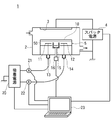
- FIG. 1 is a schematic configuration diagram of a sputtering apparatus which is an embodiment of a vacuum processing apparatus according to the present invention.
- reference numeral 2 denotes a vacuum chamber of the sputtering apparatus 1 of the present embodiment.
- the vacuum chamber 2 is connected to a vacuum exhaust system (not shown) and is configured to introduce a sputtering gas.
- a target 3 that is a film forming source is disposed in the upper part of the vacuum chamber 2.
- the target 3 is connected to a sputtering power source 4 so that a negative bias voltage is applied.
- the positive side of the sputtering power source 4 is grounded together with the vacuum chamber 2.
- an adsorption device 5 for adsorbing and holding the substrate (adsorption object) 10 is provided.
- the adsorption device 5 is of a bipolar type, and a pair of adsorption electrodes 11 and 12 are provided in a main body portion 50 made of a dielectric, and the adsorption electrodes 11 and 12 are provided on the outside of the vacuum chamber 2.
- Power is supplied from the power supply 20 via the current introduction terminals 13 and 14, respectively.
- ammeters 21 and 22 capable of measuring minute currents are connected between the current introduction terminals 13 and 14 and the suction power source 20.
- an elevating mechanism 15 is provided for placing the substrate 10 on the suction device 5 or detaching it from the suction device 5.
- a computer 23 for controlling the entire apparatus is provided outside the vacuum chamber 2, and the computer 23 includes a drive unit 16 that drives the lifting mechanism 15, ammeters 21 and 22, an adsorption power source 20, and the like. Connected to the sputter power supply 4.
- the computer 23 includes an A / D conversion board and the like, and is connected to a means (not shown) for recording current, such as a pen recorder.
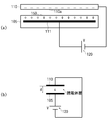
- FIG. 2A is a schematic configuration diagram showing a cross section of a full surface adsorption type adsorption apparatus.
- the suction device 105 by applying a predetermined voltage between the suction power source 120 and the substrate 110 to the suction electrode 111 provided in the suction device 105 made of a dielectric, the suction device 105. As a result, charges of opposite polarity are generated on the suction surface 150 and the back surface 110a of the substrate 110. As a result, the suction surface 150 and the substrate 110 of the suction device 105 are restrained by Coulomb force, and the substrate 110 is held on the suction surface 150.
- the Johnson Rabeck force is relatively larger than the Coulomb force.
- the Coulomb force and the Johnson Rahbek force depend on the volume resistivity of the dielectric, and the Johnson Rabeck force is dominant in the low resistivity (1 ⁇ 10 12 ⁇ ⁇ cm or less) range. It is also known that the Coulomb force becomes dominant in the range of 1 ⁇ 10 13 ⁇ ⁇ cm or more. Therefore, it is understood that a difference occurs in the adsorption force between the substrate and the adsorption device depending on the volume resistivity of the dielectric. The present invention has been made based on such knowledge.
- FIG. 3 (a) and 3 (b) schematically show a configuration example of the adsorption device according to the present invention
- FIG. 3 (a) is a sectional configuration diagram
- FIG. 3 (b) is a plan configuration diagram. .
- the adsorption device 5 of this configuration example is of a bipolar type, and the above-described adsorption electrode 11 is disposed inside a main body 50 of a rectangular plate made of a dielectric material to be described later. 12, the first adsorption electrodes 11a and 11b and the second adsorption electrodes 12a and 12b are provided.
- the first and second adsorption electrodes 11a, 11b and 12a, 12b are connected to adsorption power sources 20A, 20B having different polarities, respectively.
- the first and second adsorption electrodes 11a, 11b and 12a, 12b are each formed in a rectangular shape and arranged side by side with a predetermined interval. Yes.
- suction electrode 11a, 11b and 12a, 12b is shown typically, and is normally arrange
- an adsorption portion 51 that adsorbs the substrate 10 is provided on the adsorption-side surface of the main body portion 50.
- the adsorption part 51 of this configuration example includes a contact support part 52 that contacts and supports the back surface of the substrate 10 and a non-contact part 53 that does not contact the back surface of the substrate 10.
- the contact support part 52 is provided at the edge of the main body part 50, for example, a frame part 52a formed in a rectangular frame shape equivalent to the outer diameter of the main body part 50, and is integrally formed linearly inside the frame part 52a. It is comprised from the linear part 52b made.
- the frame portion 52a is formed so as to protrude at a constant height so that the height thereof is higher than a non-contact portion 53 described later.
- a plurality of linear portions 52b are provided, and are arranged in parallel, for example, at a predetermined interval.
- the linear part 52b is provided so that it may become a fixed height equivalent to the frame part 52a.
- the non-contact part 53 of this configuration example is provided with the surface of the main body part 50 exposed between the frame part 52a and the linear part 52b of the contact support part 52, and is formed in a planar shape. .
- each non-contact part 53 is provided so that it may become equivalent height.
- the contact support portion. 52 is preferably provided in a region other than the region corresponding to the adsorption electrodes 11 and 12 on the adsorption side surface of the main body 50, that is, in a region other than the region immediately above the adsorption electrodes 11 and 12.
- the frame portion 52 a of the contact support portion 52 is provided around a region immediately above the adsorption electrodes 11 and 12 on the adsorption side surface of the main body portion 50. Further, the linear portion 52 b of the contact support portion 52 is provided between the regions immediately above the adjacent suction electrodes 11 and 12 on the surface on the suction side of the main body portion 50.
- the frame portion 52a and the straight portion 52b of the contact support portion 52 of this configuration example are directly above the adsorption electrodes 11 and 12 on the adsorption side surface of the main body 50.
- the adsorption electrodes 11 and 12 on the adsorption-side surface of the main body 50 with respect to the frame portion 52a and the linear portion 52b of the contact support portion 52 can also be configured so as to be partially overlapped with the region immediately above.
- the adsorption portion 51 is configured such that the volume resistivity of the material of the contact support portion 52 is larger than the volume resistivity of the material of the non-contact portion 53.
- the non-contact portion 53 of the suction portion 51 is made of the same material as the main body portion 50 of the suction device 5, but is made of a material different from that of the main body portion 50 of the suction device 5 as will be described later. It is also possible to do.
- the material of the non-contact part 53 of the adsorption part 51 from the viewpoint of improving the heat transfer efficiency with the substrate 10, a material whose volume resistivity is reduced by doping with an additive is used. preferable. Examples of such a material include aluminum oxide doped with C, Ti, Cr, Fe, Ta, TiN, TiO 2, etc.
- SiO 2 volume resistivity 1 ⁇ 10 5 to 1 ⁇ 10 8 ⁇ ⁇ cm
- Ta Ti
- TiN TiO 2
- Sialon SiAlON body Resistivity: 1 ⁇ 10 14 ⁇ ⁇ cm or less
- the material of the contact support portion 52 of the adsorption portion 51 it is preferable to use the same material as that of the non-contact portion 53 and not doped with an additive.
- pyrolytic nitriding are described in correspondence with the material of the non-contact portion 53 described above.
- silicon nitride SiN volume resistivity: 1 ⁇ 10 14 to 1 ⁇ 10 15 ⁇ ⁇ cm
- aluminum nitride AlN volume resistivity
- SiO volume resistivity greater than 1 ⁇ 10 19 ⁇ ⁇ cm
- sialon siAlON volume resistivity: 1 ⁇ 10 14 ⁇ ⁇ cm greater
- the main body 50 of the adsorption device 5 of the present invention can be created by a normal ceramic manufacturing process (compression, firing, etc.).
- the contact support part 52 formed on the main-body part 50 can be produced by forming a predetermined pattern by film-forming processes, such as PVD, CVD, vapor deposition, for example.
- film-forming processes such as PVD, CVD, vapor deposition, for example.
- the following materials can also be used other than the material mentioned above.
- tantalum nitride TiN
- tungsten nitride WN
- gallium nitride GaN
- boron nitride BN
- indium nitride InN
- the like can be used as the nitride.
- oxides examples include silicon dioxide (SiO 2 ), chromium oxide (Cr 2 O 3 ), titanium oxide (TiO 2 ), titanium monoxide (TiO), zinc oxide (ZnO), and yttrium oxide (Y 2 O 3 ). It can also be used.
- carbide diamond, polyurea (PU), titanium carbide (TiC), tantalum carbide (TaC), silicon carbide (SiC), or the like can be used.
- PU polyurea
- TiC titanium carbide
- TaC tantalum carbide
- SiC silicon carbide
- polyimide PI
- polyurea PU
- silicone rubber or the like
- PI polyimide
- PU polyurea
- silicone rubber or the like
- the oxide and carbide can form the contact support portion 52 of the adsorption portion 51 by the film forming process described above.
- the contact support portion 52 of the adsorption portion 51 can be formed by a known vapor deposition polymerization method. Moreover, about the silicone rubber, the contact support part 52 of the adsorption
- the suction part 51 provided on the suction side surface of the main body part 50 is in contact with and supported by the substrate 10 and the substrate 10. Since the volume resistivity of the material of the contact support portion 52 is larger than the volume resistivity of the material of the non-contact portion 53 in the adsorption portion 51, the non-contact portion 53 does not come into contact.
- the suction force of the contact support portion 52 can be made smaller than that of the non-contact portion 53, thereby suppressing the occurrence of separation of the surface of the substrate 10 and the suction device 5 due to friction or the like at the contact portion between the suction portion 51 and the substrate 10. As a result, it is possible to prevent the generation of dust and to provide the adsorption device 5 having a longer life compared to the prior art.
- the suction force of the suction device 5 can be controlled to be uniform, so that it is possible to prevent the substrate 10 from being transported and to avoid a decrease in yield. .
- the contact support portion 52 of the suction portion 51 is provided in a region other than the region corresponding to the suction electrodes 11 and 12 on the suction side surface of the main body portion 50, Since the distance from the adsorption electrodes 11 and 12 to the surface of the non-contact part 53 of the adsorption part 51 can be made larger than the distance from the adsorption electrode 11, 12 to the surface (top) of the contact support part 52 of the adsorption part 51, The resistance value can be increased, whereby the magnitude of the Johnson Rabeck force can be controlled to a desired value. As a result, according to the present embodiment, it is possible to easily adjust the magnitude of the suction force of the contact support portion 52 and the non-contact portion 53 of the suction portion 51, and to provide a more versatile suction device 5. be able to.
- FIG. 4 is a cross-sectional configuration diagram schematically showing another configuration example of the adsorption device according to the present invention.
- the same reference numerals are given to portions corresponding to the above configuration example, and detailed description thereof will be omitted.
- the adsorbing device 5A of the present configuration example includes a main body 50 of the adsorbing device 5 described above, a base layer 50A, and a layered high resistance body (hereinafter referred to as an adsorbing side surface) provided on the adsorption side surface of the base 50A. , “High resistance layer”) 50B.
- the base 50A of the main body 50 is formed in, for example, a rectangular plate shape, and the above-described adsorption electrodes 11 and 12 are provided on the surface layer portion of one main surface thereof.
- the base 50A can be made of various ceramic materials used in general adsorption devices.
- a high resistance layer 50B made of the material of the non-contact portion 53 described above is integrally provided on the main surface of the base portion 50A on the side of the adsorption electrodes 11 and 12. That is, as the material of the high resistance layer 50B, aluminum oxide (Al 2 O 3 ), pyrolytic boron nitride (PBN), silicon nitride (SiN), aluminum nitride (AlN), silicon monoxide (SiO), sialon ( SiAlON) or the like can be used.
- the high resistance layer 50B is provided entirely on the main surface (surface) of the base 50A on the side of the adsorption electrodes 11 and 12, and is configured to cover the adsorption electrodes 11 and 12.
- the contact support portion 52 including the frame portion 52a and the linear portion 52b is provided on the high resistance layer 50B of the main body portion 50, whereby the frame portion 52a of the contact support portion 52 is provided.
- the planar portion of the high resistance layer 50B that is exposed and provided between the straight portions 52b is a non-contact portion 53.
- a material of the high resistance layer 50B of this configuration example it is preferable to use a material whose volume resistivity is reduced by doping the above-described additive.
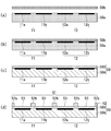
- FIG. 5A to 5D are process diagrams showing an example of a method for manufacturing the adsorption device shown in FIG.
- a base portion forming body 50a made of a constituent material of the base portion 50A of the main body portion 50 and provided with the adsorption electrodes 11 and 12 on the surface layer portion of one main surface thereof, and the main body portion 50 high-resistance body layer 50B made of a material constituting the high-resistance body layer 50B is prepared.
- the base portion forming body 50a and the high resistance layer forming body 50b are formed by forming the constituent materials of the base portion 50A and the high resistance layer 50B of the main body portion 50 into, for example, a rectangular plate shape by a known method such as press molding. .
- the high resistance layer forming body 50b is disposed on the base forming body 50a, and the base forming body 50a and the high resistance layer forming body 50b are not shown in the firing furnace. It is placed inside and heated and sintered at a predetermined temperature (firing step). As a result, as shown in FIG. 5C, the main body 50 is obtained in which the high resistance layer 50B is integrally provided on the main surface of the base 50A on the adsorption electrodes 11 and 12 side. Thereafter, the contact support portion 52 on the high resistance layer 50B is formed by the above-described film forming process or vapor deposition polymerization method. Thereby, as shown in FIG.5 (d), the main-body part 50 which has the contact support part 52 and the non-contact part 53 of the adsorption
- the main body portion 50 is formed in a plate shape and has a base portion 50A in which the adsorption electrodes 11 and 12 are provided on the surface layer portion of one main surface thereof, and the main portion 50A on the adsorption electrode 11 and 12 side of the base portion 50A. Since the high resistance layer 50B made of the material of the non-contact portion 53 is provided integrally on the surface, and the contact support portion 52 of the adsorption portion is provided on the surface of the layered high resistance body, Various methods can be used for the production of the base 50A, and various ceramic materials such as the polymer and chemical products mentioned above can be used as the material of the base 50A. An adsorption device 5A can be provided.
- the high resistance layer 50B is disposed on the main surface of the base portion 50A on the side of the adsorption electrodes 11 and 12, and the main body portion 50 is created by firing. Can be manufactured.
- the present invention is not limited to the above-described embodiment, and various changes can be made.
- the shapes of the adsorption electrodes 11 and 12, the contact support portion 52, and the non-contact portion 53 described in the above embodiment are merely examples, and various modifications can be made without exceeding the scope of the present invention.
- the present invention can be applied not only to sputtering apparatuses but also to various vacuum processing apparatuses such as vapor deposition apparatuses and etching apparatuses.
Landscapes
- Engineering & Computer Science (AREA)
- Physics & Mathematics (AREA)
- Plasma & Fusion (AREA)
- Chemical & Material Sciences (AREA)
- Analytical Chemistry (AREA)
- Mechanical Engineering (AREA)
- Container, Conveyance, Adherence, Positioning, Of Wafer (AREA)
- Physical Vapour Deposition (AREA)
Abstract
Description
このため、吸着電極と基板の間の抵抗値あるいは距離に差が生じ、不均一な吸着状態となっていた。
さらにまた、吸着面内における残留吸着力の不均一性は、プロセスの繰り返しの吸着状態に影響し、特に基板毎の温度制御のばらつきが生じるとともに、例えば逆極性の電圧印加による吸着面の残留吸着力の除去を行っても残留吸着力を完全に除去することが困難であるため、製造工程による歩留まりの低下等の信頼性の低下の問題が生じていた。
しかし、このような方法では、吸着面から基板に対する熱伝達効率を低下させ、吸着装置本来の吸着能力を最大限発揮できないという問題がある。
さらに、製造工程におけるスループット時間の短縮等による残留吸着力を起因として基板の搬送エラーや基板毎の歩留まりの低下という問題が生じることから、吸着装置の吸着力を均一となるように制御することも望まれている。
本発明では、前記吸着部の接触支持部が、前記本体部の吸着側の表面における前記吸着電極に対応する領域以外の領域に設けられている場合にも効果的である。
本発明では、前記本体部が、プレート状に形成され且つその一方の主面の表層部分に前記吸着電極が設けられた基部と、前記基部の吸着電極側の主面上に一体的に設けられ前記非接触部の材料からなる層状の高抵抗体とを有し、当該層状の高抵抗体の表面に前記吸着部の接触支持部が設けられている場合にも効果的である。
一方、本発明は、誘電体中に吸着電極を有する本体部と、前記本体部の吸着側の表面に設けられ、吸着対象物を吸着する吸着部とを有し、前記吸着部が、前記吸着対象物に接触して支持する接触支持部と、前記吸着対象物に接触しない非接触部とを有し、前記吸着部において、接触支持部の材料の体積抵抗率が、前記非接触部の材料の体積抵抗率より大きくなるように構成されている吸着装置を製造する方法であって、プレート状に形成され且つその一方の主面の表層部分に吸着電極が設けられた基部と、前記非接触部の材料からなる層状の高抵抗体とを用意し、前記基部の吸着電極側の主面上に前記層状の高抵抗体を配置し、前記基部及び前記層状の高抵抗体を焼成することによって前記基部の吸着電極側の主面上に前記層状の高抵抗体が一体的に設けられた前記本体部を作成する工程と、前記本体部の前記層状の高抵抗体の表面に前記吸着部の接触支持部を設ける工程とを有する吸着装置の製造方法である。
また、本発明は、真空槽と、前記真空槽内に設けられた上記いずれかの吸着装置とを有し、前記吸着装置によって吸着保持された基板に対して所定の処理を行うように構成されている真空処理装置である。
その結果、本発明によれば、吸着部の接触支持部と非接触部の吸着力の大きさを容易に調整することができ、より汎用性の広い吸着装置を提供することができる。
さらにまた、真空槽と、真空槽内に設けられた上記いずれかの吸着装置とを有し、吸着装置によって吸着保持された吸着対象物に対して所定の処理を行うように構成されている真空処理装置によれば、高品位の真空処理が可能な真空処理装置を提供することができる。
なお、本発明は、双極型、単極型のいずれの吸着装置にも適用することができるものである。
真空槽2内の上部には、成膜源であるターゲット3が配置されている。
このターゲット3は、スパッタ電源4に接続され、負のバイアス電圧が印加されるようになっている。なお、スパッタ電源4のプラス側は真空槽2とともにアースされている。
なお、各電流導入端子13、14と吸着電源20との間には、微小な電流を測定可能な電流計21、22が接続されている。
また、真空槽2の外部には、装置全体を制御するためのコンピュータ23が設けられ、このコンピュータ23は、上述した昇降機構15を駆動する駆動部16、電流計21、22、吸着電源20及びスパッタ電源4に接続されている。
なお、このコンピュータ23はA/D変換ボード等を備え、また例えばペンレコーダ等の電流を記録するための手段(図示せず)に接続されている。
図2(a)は、全面吸着型の吸着装置の断面を示す概略構成図である。
吸着力Fを算出するには、まず、クーロン力Fcについて考える。この場合、吸着装置105の誘電体層の誘電率ε、印加電圧V、誘電体層の距離d、基板110及び吸着装置105の帯電部分の面積Sとすると、次式が成り立つ。
Fc=1/2・ε・S(V/d)2
F=Fc+Fjr
また、クーロン力とジョンソンラーベック力は、誘電体の体積抵抗率に依存し、低抵抗率(1×10¹²Ω・cm以下)の範囲でジョンソンラーベック力が支配的となり、高抵抗率(1×10¹³Ω・cm以上)の範囲ではクーロン力が支配的となることも知られている。
よって、誘電体の体積抵抗率により、基板と吸着装置間の吸着力に差が生じることが理解される。
本発明は、かかる知見に基づいてなされたものである。
ここで、第1及び第2の吸着電極11a,11b及び12a,12bは、それぞれ極性の異なる吸着電源20A、20Bに接続されている。
なお、第1及び第2の吸着電極11a,11b及び12a,12bの配置は、模式的に示すもので、通常は、極性の異なる電極が交互になるように配置される。
本構成例の吸着部51は、基板10の裏面に接触して支持する接触支持部52と、基板10の裏面に接触しない非接触部53とを有している。
ここで、枠部52aは、後述する非接触部53に対してその高さが高くなるように一定の高さで突出して形成されている。
なお、直線部52bは、枠部52aと同等の一定の高さとなるように設けられている。
また、接触支持部52の直線部52bは、本体部50の吸着側の表面において隣接する吸着電極11、12の直上の領域の間に設けられている。
本構成例の場合、吸着部51の非接触部53は、吸着装置5の本体部50と同じ材料によって構成されているが、後述するように、吸着装置5の本体部50と異なる材料で構成することも可能である。
このような材料としては、例えば、C、Ti、Cr、Fe、Ta、TiN、TiO2などをドープした酸化アルミニウム(Al2O3 体積抵抗率:1×10⁷~1×10¹²Ω・cm)、CxHy系の物質をドープした熱分解窒化ホウ素(PBN 体積抵抗率:1×10⁸~1×10¹²Ω・cm)、Ga、In、Al、TiN、TiO2などをドープした窒化ケイ素(SiN 体積抵抗率:1×10⁸~1×10¹²Ω・cm)、Ti、TiN、TiO2、Taなどをドープした窒化アルミニウム(AlN 体積抵抗率:1×10²~1×10¹⁵Ω・cm)、Ta、Ti、TiN、TiO2などをドープした二酸化ケイ素(SiO2 体積抵抗率:1×10⁵~1×10⁸Ω・cm)、Ta、Ti、TiN、TiO2などをドープしたサイアロン(SiAlON 体積抵抗率:1×10¹⁴Ω・cm以下)、等があげられる。
また、本体部50上に形成される接触支持部52は、例えば、PVD、CVD、蒸着等の成膜プロセスによって所定パターンを形成することによって作成することができる。
なお、吸着部51の接触支持部52の材料としては、上述した材料の他、以下のような材料を用いることもできる。
また、シリコーンゴムについては、成型加工したシートを貼り合せることによって吸着部51の接触支持部52を作成することができる。
その結果、本実施の形態によれば、吸着部51の接触支持部52と非接触部53の吸着力の大きさを容易に調整することができ、より汎用性の広い吸着装置5を提供することができる。
この基部50Aは、一般的な吸着装置に用いられている種々のセラミックス材料を使用することができる。
すなわち、高抵抗体層50Bの材料としては、酸化アルミニウム(Al2O3)、熱分解窒化ホウ素(PBN)、窒化ケイ素(SiN)、窒化アルミニウム(AlN)、一酸化ケイ素(SiO)、サイアロン(SiAlON)等を用いることができる。
この高抵抗体層50Bは、基部50Aの吸着電極11、12側の主面(表面)上に全面的に設けられ、これにより吸着電極11、12を覆うように構成されている。
本構成例の高抵抗体層50Bの材料としては、上述した添加物のドープによって体積抵抗率を低下させた材料を用いることが好ましい。
図5(a)に示すように、まず、本体部50の基部50Aの構成材料からなり、その一方の主面の表層部分に吸着電極11、12が設けられた基部形成体50aと、本体部50の高抵抗体層50Bの構成材料からなる高抵抗体層形成体50bとを用意する。
これら基部形成体50a及び高抵抗体層形成体50bは、本体部50の基部50A及び高抵抗体層50Bの構成材料を、プレス成形等の公知の方法によって例えば矩形プレート形状に形成したものである。
これにより、図5(c)に示すように、基部50Aの吸着電極11、12側の主面上に高抵抗体層50Bが一体的に設けられた本体部50が得られる。
その後、上述した成膜プロセスや蒸着重合法によって高抵抗体層50B上の接触支持部52を作成する。
これにより、図5(d)に示すように、吸着部51の接触支持部52及び非接触部53を有する本体部50を得ることができる。
例えば、上記実施の形態に記載した吸着電極11、12、接触支持部52、非接触部53の形状は一例であり、本発明の範囲を超えない限り、種々の変更を行うことができる。
さらに、本発明はスパッタリング装置のみならず、例えば蒸着装置やエッチング装置等の種々の真空処理装置に適用することができる。
2…真空槽
3…ターゲット
4…スパッタ電源
5…吸着装置
10…基板(吸着対象物)
11、11a、11b、12、12a、12b…吸着電極
20…吸着電源
50…本体部
51…吸着部
52…接触支持部
53…非接触部
Claims (5)
- 誘電体中に吸着電極を有する本体部と、
前記本体部の吸着側の表面に設けられ、吸着対象物を吸着する吸着部とを有し、
前記吸着部が、前記吸着対象物に接触して支持する接触支持部と、前記吸着対象物に接触しない非接触部とを有し、
前記吸着部において、前記接触支持部の材料の体積抵抗率が、前記非接触部の材料の体積抵抗率より大きくなるように構成されている吸着装置。 - 前記吸着部の接触支持部が、前記本体部の吸着側の表面における前記吸着電極に対応する領域以外の領域に設けられている請求項1記載の吸着装置。
- 前記本体部が、プレート状に形成され且つその一方の主面の表層部分に前記吸着電極が設けられた基部と、前記基部の吸着電極側の主面上に一体的に設けられ前記非接触部の材料からなる層状の高抵抗体とを有し、
当該層状の高抵抗体の表面に前記吸着部の接触支持部が設けられている請求項1又は2のいずれか1項記載の吸着装置。 - 誘電体中に吸着電極を有する本体部と、前記本体部の吸着側の表面に設けられ、吸着対象物を吸着する吸着部とを有し、前記吸着部が、前記吸着対象物に接触して支持する接触支持部と、前記吸着対象物に接触しない非接触部とを有し、前記吸着部において、接触支持部の材料の体積抵抗率が、前記非接触部の材料の体積抵抗率より大きくなるように構成されている吸着装置を製造する方法であって、
プレート状に形成され且つその一方の主面の表層部分に吸着電極が設けられた基部と、前記非接触部の材料からなる層状の高抵抗体とを用意し、
前記基部の吸着電極側の主面上に前記層状の高抵抗体を配置し、前記基部及び前記層状の高抵抗体を焼成することによって前記基部の吸着電極側の主面上に前記層状の高抵抗体が一体的に設けられた前記本体部を作成する工程と、
前記本体部の前記層状の高抵抗体の表面に前記吸着部の接触支持部を設ける工程とを有する吸着装置の製造方法。 - 真空槽と、
前記真空槽内に設けられた吸着装置とを備え、
前記吸着装置は、誘電体中に吸着電極を有する本体部と、前記本体部の吸着側の表面に設けられ、吸着対象物を吸着する吸着部とを有し、前記吸着部が、前記吸着対象物に接触して支持する接触支持部と、前記吸着対象物に接触しない非接触部とを有し、前記吸着部において、前記接触支持部の材料の体積抵抗率が、前記非接触部の材料の体積抵抗率より大きくなるように構成され、
前記吸着装置によって吸着保持された基板に対して所定の処理を行うように構成されている真空処理装置。
Priority Applications (4)
| Application Number | Priority Date | Filing Date | Title |
|---|---|---|---|
| JP2017510247A JP6312926B2 (ja) | 2015-04-02 | 2016-04-01 | 吸着方法及び真空処理方法 |
| KR1020177031557A KR101902806B1 (ko) | 2015-04-02 | 2016-04-01 | 흡착방법 및 진공처리방법 |
| CN201680032106.7A CN107615474B (zh) | 2015-04-02 | 2016-04-01 | 吸附装置、吸附装置的制造方法、以及真空处理装置 |
| US15/719,947 US10720858B2 (en) | 2015-04-02 | 2017-09-29 | Attraction device, method for producing attraction device, and vacuum processing device |
Applications Claiming Priority (2)
| Application Number | Priority Date | Filing Date | Title |
|---|---|---|---|
| JP2015-075938 | 2015-04-02 | ||
| JP2015075938 | 2015-04-02 |
Related Child Applications (1)
| Application Number | Title | Priority Date | Filing Date |
|---|---|---|---|
| US15/719,947 Continuation US10720858B2 (en) | 2015-04-02 | 2017-09-29 | Attraction device, method for producing attraction device, and vacuum processing device |
Publications (1)
| Publication Number | Publication Date |
|---|---|
| WO2016159342A1 true WO2016159342A1 (ja) | 2016-10-06 |
Family
ID=57006896
Family Applications (1)
| Application Number | Title | Priority Date | Filing Date |
|---|---|---|---|
| PCT/JP2016/060909 Ceased WO2016159342A1 (ja) | 2015-04-02 | 2016-04-01 | 吸着装置、吸着装置の製造方法、及び真空処理装置 |
Country Status (6)
| Country | Link |
|---|---|
| US (1) | US10720858B2 (ja) |
| JP (1) | JP6312926B2 (ja) |
| KR (1) | KR101902806B1 (ja) |
| CN (1) | CN107615474B (ja) |
| TW (1) | TWI647787B (ja) |
| WO (1) | WO2016159342A1 (ja) |
Cited By (1)
| Publication number | Priority date | Publication date | Assignee | Title |
|---|---|---|---|---|
| KR20250136375A (ko) | 2023-02-24 | 2025-09-16 | 도카로 가부시키가이샤 | 플라즈마 처리 장치용 부품 |
Citations (2)
| Publication number | Priority date | Publication date | Assignee | Title |
|---|---|---|---|---|
| JP2006287210A (ja) * | 2005-03-07 | 2006-10-19 | Ngk Insulators Ltd | 静電チャック及びその製造方法 |
| JP2009302347A (ja) * | 2008-06-13 | 2009-12-24 | Shinko Electric Ind Co Ltd | 静電チャック及び基板温調固定装置 |
Family Cites Families (11)
| Publication number | Priority date | Publication date | Assignee | Title |
|---|---|---|---|---|
| JP3324268B2 (ja) | 1994-04-15 | 2002-09-17 | 東陶機器株式会社 | 静電吸着方法 |
| JP4166379B2 (ja) | 1999-07-30 | 2008-10-15 | 株式会社アルバック | 基板搬送装置 |
| JP4342691B2 (ja) | 2000-04-24 | 2009-10-14 | 株式会社アルバック | 静電吸着装置及び真空処理装置 |
| KR100511854B1 (ko) * | 2002-06-18 | 2005-09-02 | 아네르바 가부시키가이샤 | 정전 흡착 장치 |
| TW200735254A (en) * | 2006-03-03 | 2007-09-16 | Ngk Insulators Ltd | Electrostatic chuck and producing method thereof |
| JP4974873B2 (ja) * | 2007-12-26 | 2012-07-11 | 新光電気工業株式会社 | 静電チャック及び基板温調固定装置 |
| US8730644B2 (en) | 2008-07-08 | 2014-05-20 | Creative Technology Corporation | Bipolar electrostatic chuck |
| WO2012026421A1 (ja) * | 2010-08-24 | 2012-03-01 | 株式会社クリエイティブ テクノロジー | 静電チャック装置及びその製造方法 |
| US8804299B2 (en) * | 2011-02-14 | 2014-08-12 | Applied Materials Israel, Ltd. | Electrostatic chuck and a method for supporting a wafer |
| JP5505667B2 (ja) * | 2011-09-30 | 2014-05-28 | Toto株式会社 | 交流駆動静電チャック |
| CN104081285B (zh) * | 2012-02-03 | 2017-06-13 | Asml荷兰有限公司 | 衬底保持器和制造衬底保持器的方法 |
-
2016
- 2016-04-01 WO PCT/JP2016/060909 patent/WO2016159342A1/ja not_active Ceased
- 2016-04-01 CN CN201680032106.7A patent/CN107615474B/zh active Active
- 2016-04-01 KR KR1020177031557A patent/KR101902806B1/ko active Active
- 2016-04-01 JP JP2017510247A patent/JP6312926B2/ja active Active
- 2016-04-01 TW TW105110716A patent/TWI647787B/zh active
-
2017
- 2017-09-29 US US15/719,947 patent/US10720858B2/en active Active
Patent Citations (2)
| Publication number | Priority date | Publication date | Assignee | Title |
|---|---|---|---|---|
| JP2006287210A (ja) * | 2005-03-07 | 2006-10-19 | Ngk Insulators Ltd | 静電チャック及びその製造方法 |
| JP2009302347A (ja) * | 2008-06-13 | 2009-12-24 | Shinko Electric Ind Co Ltd | 静電チャック及び基板温調固定装置 |
Cited By (1)
| Publication number | Priority date | Publication date | Assignee | Title |
|---|---|---|---|---|
| KR20250136375A (ko) | 2023-02-24 | 2025-09-16 | 도카로 가부시키가이샤 | 플라즈마 처리 장치용 부품 |
Also Published As
| Publication number | Publication date |
|---|---|
| KR20170134569A (ko) | 2017-12-06 |
| JP6312926B2 (ja) | 2018-04-18 |
| CN107615474A (zh) | 2018-01-19 |
| TW201642387A (zh) | 2016-12-01 |
| TWI647787B (zh) | 2019-01-11 |
| US20180175749A1 (en) | 2018-06-21 |
| CN107615474B (zh) | 2020-12-01 |
| US10720858B2 (en) | 2020-07-21 |
| KR101902806B1 (ko) | 2018-10-01 |
| JPWO2016159342A1 (ja) | 2018-01-11 |
Similar Documents
| Publication | Publication Date | Title |
|---|---|---|
| US9472434B2 (en) | Locally heated multi-zone substrate support | |
| JP6064908B2 (ja) | 静電チャック装置 | |
| JP4774025B2 (ja) | 吸着装置、搬送装置 | |
| TWI637459B (zh) | 高溫製程應用上的靜電夾盤 | |
| JP2001035907A (ja) | 吸着装置 | |
| JP6279149B2 (ja) | 吸着装置及び真空処理装置 | |
| CN111417742B (zh) | 处理装置 | |
| JP2020184575A (ja) | ロボット用ハンド、ウェハ搬送用ロボット及びウェハ搬送装置 | |
| JP6312926B2 (ja) | 吸着方法及び真空処理方法 | |
| JP4339306B2 (ja) | 吸着方法 | |
| US9518326B2 (en) | Method for forming an electrostatic chuck using film printing technology | |
| JP2007109827A (ja) | 静電チャック | |
| JP5225043B2 (ja) | 静電チャック | |
| JP2020205350A (ja) | 静電チャックおよびその運転方法 | |
| CN111433903A (zh) | 晶圆支撑装置 | |
| JP4341592B2 (ja) | ガラス基板吸着用静電チャック及びガラス基板吸着方法 | |
| JP2005116686A (ja) | 双極型静電チャック | |
| JP4495687B2 (ja) | 静電チャック | |
| JP4166379B2 (ja) | 基板搬送装置 | |
| JP2008159900A (ja) | 静電チャック付きセラミックヒーター | |
| JP2008205509A (ja) | 絶縁基板搬送方法、位置合わせ方法 | |
| JP2008205508A (ja) | 基板搬送装置、真空処理装置 | |
| JP2006054445A (ja) | 吸着装置 | |
| JPWO2011158444A1 (ja) | 搬送処理装置及び処理装置 |
Legal Events
| Date | Code | Title | Description |
|---|---|---|---|
| 121 | Ep: the epo has been informed by wipo that ep was designated in this application |
Ref document number: 16773222 Country of ref document: EP Kind code of ref document: A1 |
|
| ENP | Entry into the national phase |
Ref document number: 2017510247 Country of ref document: JP Kind code of ref document: A |
|
| NENP | Non-entry into the national phase |
Ref country code: DE |
|
| ENP | Entry into the national phase |
Ref document number: 20177031557 Country of ref document: KR Kind code of ref document: A |
|
| 122 | Ep: pct application non-entry in european phase |
Ref document number: 16773222 Country of ref document: EP Kind code of ref document: A1 |