WO2016158180A1 - 薄膜トランジスタの製造方法、および薄膜トランジスタ - Google Patents
薄膜トランジスタの製造方法、および薄膜トランジスタ Download PDFInfo
- Publication number
- WO2016158180A1 WO2016158180A1 PCT/JP2016/056477 JP2016056477W WO2016158180A1 WO 2016158180 A1 WO2016158180 A1 WO 2016158180A1 JP 2016056477 W JP2016056477 W JP 2016056477W WO 2016158180 A1 WO2016158180 A1 WO 2016158180A1
- Authority
- WO
- WIPO (PCT)
- Prior art keywords
- oxide semiconductor
- semiconductor layer
- thin film
- film transistor
- drain electrode
- Prior art date
- Legal status (The legal status is an assumption and is not a legal conclusion. Google has not performed a legal analysis and makes no representation as to the accuracy of the status listed.)
- Ceased
Links
Images










Classifications
-
- H—ELECTRICITY
- H10—SEMICONDUCTOR DEVICES; ELECTRIC SOLID-STATE DEVICES NOT OTHERWISE PROVIDED FOR
- H10D—INORGANIC ELECTRIC SEMICONDUCTOR DEVICES
- H10D30/00—Field-effect transistors [FET]
- H10D30/60—Insulated-gate field-effect transistors [IGFET]
- H10D30/67—Thin-film transistors [TFT]
- H10D30/674—Thin-film transistors [TFT] characterised by the active materials
- H10D30/6755—Oxide semiconductors, e.g. zinc oxide, copper aluminium oxide or cadmium stannate
-
- H—ELECTRICITY
- H10—SEMICONDUCTOR DEVICES; ELECTRIC SOLID-STATE DEVICES NOT OTHERWISE PROVIDED FOR
- H10D—INORGANIC ELECTRIC SEMICONDUCTOR DEVICES
- H10D30/00—Field-effect transistors [FET]
- H10D30/60—Insulated-gate field-effect transistors [IGFET]
- H10D30/67—Thin-film transistors [TFT]
-
- H—ELECTRICITY
- H10—SEMICONDUCTOR DEVICES; ELECTRIC SOLID-STATE DEVICES NOT OTHERWISE PROVIDED FOR
- H10D—INORGANIC ELECTRIC SEMICONDUCTOR DEVICES
- H10D30/00—Field-effect transistors [FET]
- H10D30/60—Insulated-gate field-effect transistors [IGFET]
- H10D30/67—Thin-film transistors [TFT]
- H10D30/6729—Thin-film transistors [TFT] characterised by the electrodes
- H10D30/6737—Thin-film transistors [TFT] characterised by the electrodes characterised by the electrode materials
- H10D30/6739—Conductor-insulator-semiconductor electrodes
-
- H—ELECTRICITY
- H10—SEMICONDUCTOR DEVICES; ELECTRIC SOLID-STATE DEVICES NOT OTHERWISE PROVIDED FOR
- H10D—INORGANIC ELECTRIC SEMICONDUCTOR DEVICES
- H10D30/00—Field-effect transistors [FET]
- H10D30/60—Insulated-gate field-effect transistors [IGFET]
- H10D30/67—Thin-film transistors [TFT]
- H10D30/6758—Thin-film transistors [TFT] characterised by the insulating substrates
-
- H—ELECTRICITY
- H10—SEMICONDUCTOR DEVICES; ELECTRIC SOLID-STATE DEVICES NOT OTHERWISE PROVIDED FOR
- H10D—INORGANIC ELECTRIC SEMICONDUCTOR DEVICES
- H10D62/00—Semiconductor bodies, or regions thereof, of devices having potential barriers
- H10D62/80—Semiconductor bodies, or regions thereof, of devices having potential barriers characterised by the materials
-
- H—ELECTRICITY
- H10—SEMICONDUCTOR DEVICES; ELECTRIC SOLID-STATE DEVICES NOT OTHERWISE PROVIDED FOR
- H10D—INORGANIC ELECTRIC SEMICONDUCTOR DEVICES
- H10D62/00—Semiconductor bodies, or regions thereof, of devices having potential barriers
- H10D62/80—Semiconductor bodies, or regions thereof, of devices having potential barriers characterised by the materials
- H10D62/875—Semiconductor bodies, or regions thereof, of devices having potential barriers characterised by the materials being semiconductor metal oxide, e.g. InGaZnO
-
- H—ELECTRICITY
- H10—SEMICONDUCTOR DEVICES; ELECTRIC SOLID-STATE DEVICES NOT OTHERWISE PROVIDED FOR
- H10D—INORGANIC ELECTRIC SEMICONDUCTOR DEVICES
- H10D84/00—Integrated devices formed in or on semiconductor substrates that comprise only semiconducting layers, e.g. on Si wafers or on GaAs-on-Si wafers
- H10D84/01—Manufacture or treatment
- H10D84/0123—Integrating together multiple components covered by H10D12/00 or H10D30/00, e.g. integrating multiple IGBTs
- H10D84/0126—Integrating together multiple components covered by H10D12/00 or H10D30/00, e.g. integrating multiple IGBTs the components including insulated gates, e.g. IGFETs
- H10D84/0165—Integrating together multiple components covered by H10D12/00 or H10D30/00, e.g. integrating multiple IGBTs the components including insulated gates, e.g. IGFETs the components including complementary IGFETs, e.g. CMOS devices
-
- H—ELECTRICITY
- H10—SEMICONDUCTOR DEVICES; ELECTRIC SOLID-STATE DEVICES NOT OTHERWISE PROVIDED FOR
- H10D—INORGANIC ELECTRIC SEMICONDUCTOR DEVICES
- H10D86/00—Integrated devices formed in or on insulating or conducting substrates, e.g. formed in silicon-on-insulator [SOI] substrates or on stainless steel or glass substrates
- H10D86/40—Integrated devices formed in or on insulating or conducting substrates, e.g. formed in silicon-on-insulator [SOI] substrates or on stainless steel or glass substrates characterised by multiple TFTs
- H10D86/411—Integrated devices formed in or on insulating or conducting substrates, e.g. formed in silicon-on-insulator [SOI] substrates or on stainless steel or glass substrates characterised by multiple TFTs characterised by materials, geometry or structure of the substrates
-
- H—ELECTRICITY
- H10—SEMICONDUCTOR DEVICES; ELECTRIC SOLID-STATE DEVICES NOT OTHERWISE PROVIDED FOR
- H10D—INORGANIC ELECTRIC SEMICONDUCTOR DEVICES
- H10D86/00—Integrated devices formed in or on insulating or conducting substrates, e.g. formed in silicon-on-insulator [SOI] substrates or on stainless steel or glass substrates
- H10D86/40—Integrated devices formed in or on insulating or conducting substrates, e.g. formed in silicon-on-insulator [SOI] substrates or on stainless steel or glass substrates characterised by multiple TFTs
- H10D86/421—Integrated devices formed in or on insulating or conducting substrates, e.g. formed in silicon-on-insulator [SOI] substrates or on stainless steel or glass substrates characterised by multiple TFTs having a particular composition, shape or crystalline structure of the active layer
- H10D86/423—Integrated devices formed in or on insulating or conducting substrates, e.g. formed in silicon-on-insulator [SOI] substrates or on stainless steel or glass substrates characterised by multiple TFTs having a particular composition, shape or crystalline structure of the active layer comprising semiconductor materials not belonging to the Group IV, e.g. InGaZnO
-
- H—ELECTRICITY
- H10—SEMICONDUCTOR DEVICES; ELECTRIC SOLID-STATE DEVICES NOT OTHERWISE PROVIDED FOR
- H10D—INORGANIC ELECTRIC SEMICONDUCTOR DEVICES
- H10D86/00—Integrated devices formed in or on insulating or conducting substrates, e.g. formed in silicon-on-insulator [SOI] substrates or on stainless steel or glass substrates
- H10D86/40—Integrated devices formed in or on insulating or conducting substrates, e.g. formed in silicon-on-insulator [SOI] substrates or on stainless steel or glass substrates characterised by multiple TFTs
- H10D86/471—Integrated devices formed in or on insulating or conducting substrates, e.g. formed in silicon-on-insulator [SOI] substrates or on stainless steel or glass substrates characterised by multiple TFTs having different architectures, e.g. having both top-gate and bottom-gate TFTs
-
- H—ELECTRICITY
- H10—SEMICONDUCTOR DEVICES; ELECTRIC SOLID-STATE DEVICES NOT OTHERWISE PROVIDED FOR
- H10D—INORGANIC ELECTRIC SEMICONDUCTOR DEVICES
- H10D86/00—Integrated devices formed in or on insulating or conducting substrates, e.g. formed in silicon-on-insulator [SOI] substrates or on stainless steel or glass substrates
- H10D86/40—Integrated devices formed in or on insulating or conducting substrates, e.g. formed in silicon-on-insulator [SOI] substrates or on stainless steel or glass substrates characterised by multiple TFTs
- H10D86/60—Integrated devices formed in or on insulating or conducting substrates, e.g. formed in silicon-on-insulator [SOI] substrates or on stainless steel or glass substrates characterised by multiple TFTs wherein the TFTs are in active matrices
-
- H—ELECTRICITY
- H10—SEMICONDUCTOR DEVICES; ELECTRIC SOLID-STATE DEVICES NOT OTHERWISE PROVIDED FOR
- H10D—INORGANIC ELECTRIC SEMICONDUCTOR DEVICES
- H10D99/00—Subject matter not provided for in other groups of this subclass
-
- H—ELECTRICITY
- H10—SEMICONDUCTOR DEVICES; ELECTRIC SOLID-STATE DEVICES NOT OTHERWISE PROVIDED FOR
- H10P—GENERIC PROCESSES OR APPARATUS FOR THE MANUFACTURE OR TREATMENT OF DEVICES COVERED BY CLASS H10
- H10P14/00—Formation of materials, e.g. in the shape of layers or pillars
- H10P14/20—Formation of materials, e.g. in the shape of layers or pillars of semiconductor materials
- H10P14/29—Formation of materials, e.g. in the shape of layers or pillars of semiconductor materials characterised by the substrates
- H10P14/2901—Materials
- H10P14/2922—Materials being non-crystalline insulating materials, e.g. glass or polymers
-
- H—ELECTRICITY
- H10—SEMICONDUCTOR DEVICES; ELECTRIC SOLID-STATE DEVICES NOT OTHERWISE PROVIDED FOR
- H10P—GENERIC PROCESSES OR APPARATUS FOR THE MANUFACTURE OR TREATMENT OF DEVICES COVERED BY CLASS H10
- H10P14/00—Formation of materials, e.g. in the shape of layers or pillars
- H10P14/20—Formation of materials, e.g. in the shape of layers or pillars of semiconductor materials
- H10P14/34—Deposited materials, e.g. layers
- H10P14/3402—Deposited materials, e.g. layers characterised by the chemical composition
- H10P14/3434—Deposited materials, e.g. layers characterised by the chemical composition being oxide semiconductor materials
-
- H—ELECTRICITY
- H10—SEMICONDUCTOR DEVICES; ELECTRIC SOLID-STATE DEVICES NOT OTHERWISE PROVIDED FOR
- H10P—GENERIC PROCESSES OR APPARATUS FOR THE MANUFACTURE OR TREATMENT OF DEVICES COVERED BY CLASS H10
- H10P14/00—Formation of materials, e.g. in the shape of layers or pillars
- H10P14/40—Formation of materials, e.g. in the shape of layers or pillars of conductive or resistive materials
-
- H—ELECTRICITY
- H10—SEMICONDUCTOR DEVICES; ELECTRIC SOLID-STATE DEVICES NOT OTHERWISE PROVIDED FOR
- H10P—GENERIC PROCESSES OR APPARATUS FOR THE MANUFACTURE OR TREATMENT OF DEVICES COVERED BY CLASS H10
- H10P50/00—Etching of wafers, substrates or parts of devices
- H10P50/69—Etching of wafers, substrates or parts of devices using masks for semiconductor materials
-
- H—ELECTRICITY
- H10—SEMICONDUCTOR DEVICES; ELECTRIC SOLID-STATE DEVICES NOT OTHERWISE PROVIDED FOR
- H10P—GENERIC PROCESSES OR APPARATUS FOR THE MANUFACTURE OR TREATMENT OF DEVICES COVERED BY CLASS H10
- H10P76/00—Manufacture or treatment of masks on semiconductor bodies, e.g. by lithography or photolithography
- H10P76/20—Manufacture or treatment of masks on semiconductor bodies, e.g. by lithography or photolithography of masks comprising organic materials
- H10P76/204—Manufacture or treatment of masks on semiconductor bodies, e.g. by lithography or photolithography of masks comprising organic materials of organic photoresist masks
- H10P76/2041—Photolithographic processes
-
- H—ELECTRICITY
- H10—SEMICONDUCTOR DEVICES; ELECTRIC SOLID-STATE DEVICES NOT OTHERWISE PROVIDED FOR
- H10P—GENERIC PROCESSES OR APPARATUS FOR THE MANUFACTURE OR TREATMENT OF DEVICES COVERED BY CLASS H10
- H10P95/00—Generic processes or apparatus for manufacture or treatments not covered by the other groups of this subclass
-
- H—ELECTRICITY
- H10—SEMICONDUCTOR DEVICES; ELECTRIC SOLID-STATE DEVICES NOT OTHERWISE PROVIDED FOR
- H10W—GENERIC PACKAGES, INTERCONNECTIONS, CONNECTORS OR OTHER CONSTRUCTIONAL DETAILS OF DEVICES COVERED BY CLASS H10
- H10W20/00—Interconnections in chips, wafers or substrates
- H10W20/01—Manufacture or treatment
-
- H—ELECTRICITY
- H10—SEMICONDUCTOR DEVICES; ELECTRIC SOLID-STATE DEVICES NOT OTHERWISE PROVIDED FOR
- H10D—INORGANIC ELECTRIC SEMICONDUCTOR DEVICES
- H10D86/00—Integrated devices formed in or on insulating or conducting substrates, e.g. formed in silicon-on-insulator [SOI] substrates or on stainless steel or glass substrates
- H10D86/01—Manufacture or treatment
- H10D86/021—Manufacture or treatment of multiple TFTs
- H10D86/0212—Manufacture or treatment of multiple TFTs comprising manufacture, treatment or coating of substrates
-
- H—ELECTRICITY
- H10—SEMICONDUCTOR DEVICES; ELECTRIC SOLID-STATE DEVICES NOT OTHERWISE PROVIDED FOR
- H10D—INORGANIC ELECTRIC SEMICONDUCTOR DEVICES
- H10D86/00—Integrated devices formed in or on insulating or conducting substrates, e.g. formed in silicon-on-insulator [SOI] substrates or on stainless steel or glass substrates
- H10D86/01—Manufacture or treatment
- H10D86/021—Manufacture or treatment of multiple TFTs
- H10D86/0221—Manufacture or treatment of multiple TFTs comprising manufacture, treatment or patterning of TFT semiconductor bodies
Definitions
- the present invention relates to a thin film transistor using an oxide semiconductor for a semiconductor layer.
- PEN polyethylene naphthalate
- PI polyimide
- the semiconductor layer an oxide semiconductor that can be formed at a temperature lower than the heat resistant temperature of the film is used.
- a photolithography method or a printing method is used for manufacturing a source electrode, a drain electrode, and a gate electrode included in the thin film transistor.
- Patent Document 1 describes a thin film transistor in which a gate insulating film is used as a substrate (base material) and each electrode and a semiconductor layer are formed by a printing method.
- thermal processes such as film formation and heat treatment are repeated.
- vacuum deposition such as sputtering or vapor deposition or drying after a coating process.
- the base material may be stretched or contracted to change the dimensions of the base material.
- a heat treatment is performed at the time of forming each layer, and the dimensions of the base material are changed for each process. There was a change. For this reason, it is difficult to control the formation positions of the source electrode and the drain electrode with respect to the gate electrode. As a result, the transistor as designed cannot be manufactured, and the transistor performance varies and the product yield may deteriorate.
- an object of the present invention is to provide a method for manufacturing a thin film transistor capable of suppressing a decrease in performance and variations, and a thin film transistor.
- the manufacturing method of the thin film transistor of the present invention includes a step of forming an oxide semiconductor layer on one main surface of a substrate, a first conductive layer on the oxide semiconductor layer, Forming a second conductive layer on the other main surface of the material, forming a mask layer on the first conductive layer and the second conductive layer, and the first conductive layer and the second conductive layer.
- a step of forming a gate electrode on the main surface is a step of forming an oxide semiconductor layer on one main surface of a substrate, a first conductive layer on the oxide semiconductor layer, Forming a second conductive layer on the other main surface of the material, forming a mask layer on the first conductive layer and the second conductive layer, and the first conductive layer and the second conductive layer.
- the method for manufacturing a thin film transistor of the present invention includes a step of forming a mask layer collectively on the first conductive layer and the second conductive layer, even if the base material is thermally stretched or contracted, the source electrode It becomes easy to maintain the positional relationship between the drain electrode and the gate electrode. As a result, it is possible to suppress degradation in the performance of the transistor due to the displacement of the gate electrode with respect to the source electrode and the drain electrode.
- the base material also serves as a gate insulating film, it is not necessary to separately provide a gate insulating film such as a silicon oxide film, and the thickness of the entire transistor can be suppressed.
- the channel length can be controlled to 10 ⁇ m or less, and the circuit can be miniaturized.
- the method for manufacturing a thin film transistor of the present invention after forming a source electrode and a drain electrode, a step of forming a mask layer so as to cover between the source electrode and the drain electrode, an oxide semiconductor layer is contacted with an etching solution, It is preferable that the method further includes a step of removing a region of the oxide semiconductor layer that is not covered with the source electrode, the drain electrode, and the mask layer. By etching the oxide semiconductor layer in this manner, the etching width between the source electrode and the semiconductor layer and the etching width between the drain electrode and the semiconductor layer can be made uniform.
- a terminal electrode or a via electrode can be formed on the substrate.
- the oxide semiconductor layer preferably contains In, Ga, Zn, and O. Since the electron mobility of IGZO is as high as 10 cm 2 / V ⁇ sec among oxide semiconductors, the processing speed of the transistor can be improved.
- the first conductive layer and the second conductive layer are made of Cu. This is because Cu has high electrical conductivity, is inexpensive, and has excellent heat resistance.
- the mask layer is formed of a dry film resist. Compared with the case where the mask layer is formed of a liquid resist, when the mask layer is formed of a dry film resist, it is not necessary to dry the solvent after applying the resist, so that productivity can be improved. .
- the thin film transistor of the present invention capable of achieving the above object includes a base material, an oxide semiconductor layer formed on one main surface of the base material, and a source electrode formed on the oxide semiconductor layer. And a drain electrode formed on the oxide semiconductor layer and a gate electrode formed on the other main surface of the base material.
- the base material also serves as a gate insulating film, it is not necessary to separately provide a gate insulating film such as a silicon oxide film, and the thickness of the entire transistor can be suppressed. Further, there is no variation in transistor performance due to the occurrence of pinholes in the gate insulating film and variations in quality such as film thickness.
- the oxide semiconductor layer preferably contains In, Ga, Zn, and O.
- the source electrode, the drain electrode, and the gate electrode are formed by batch photolithography and batch wet etching.
- the channel length can be controlled to 10 ⁇ m or less, and the circuit can be miniaturized.
- the source electrode, the drain electrode, and the gate electrode are formed by batch photolithography and batch wet etching, the source electrode, the drain electrode, and the gate electrode can be formed even if the substrate is thermally stretched or contracted. It becomes easy to maintain the positional relationship. As a result, it is possible to suppress degradation in the performance of the transistor due to the displacement of the gate electrode with respect to the source electrode and the drain electrode.
- the thin film transistor of the present invention that can achieve the above object is formed on a base material, a first oxide semiconductor layer formed on one main surface of the base material, and the other main surface of the base material. And a first gate electrode formed on the first oxide semiconductor layer and a first oxide formed on the second oxide semiconductor layer.
- the base material also serves as a gate insulating film, it is not necessary to separately provide a gate insulating film such as a silicon oxide film, and the thickness of the entire transistor can be suppressed.
- the thin film transistor of the present invention there is no variation in transistor performance due to the occurrence of pinholes in the gate insulating film and variations in quality such as film thickness.
- two transistors are arranged in different directions with a base material interposed therebetween. Therefore, the arrangement interval between adjacent transistors can be reduced, and the degree of circuit integration can be increased.
- first source electrode or the first drain electrode and the second source electrode or the second drain electrode overlap with each other. Since the arrangement interval between adjacent transistors can be further reduced, the degree of circuit integration can be further increased.
- the conductivity type of the first oxide semiconductor layer and the conductivity type of the second oxide semiconductor layer have opposite polarities, and the first transistor and the second transistor are configured to be complementary.
- the first transistor and the second transistor can be arranged in a CMOS structure in terms of a metal oxide semiconductor (MOS).
- MOS metal oxide semiconductor
- the first drain electrode and the second drain electrode are arranged so as to overlap each other, and a through hole is formed in the base material in a region where the first drain electrode and the second drain electrode overlap, and the first drain electrode and the second drain electrode are formed through the through hole.
- a drain electrode is preferably connected. Since the first drain electrode and the second drain electrode are arranged so as to overlap the through hole, the arrangement interval between adjacent transistors can be further reduced, and the degree of circuit integration can be further increased. In addition, since the first drain electrode and the second drain electrode are connected in the through hole, the wiring length necessary for connecting the first drain electrode and the second drain electrode can be shortened, and a space for wiring is separately provided. There is no need to secure.
- the first oxide semiconductor layer or the second oxide semiconductor layer preferably contains In, Ga, Zn, and O.
- the base material is formed of a polymer film and the thickness of the base material is 0.1 ⁇ m or more and 50 ⁇ m or less. If the base material is a polymer film having a film thickness of 0.1 ⁇ m or more and 50 ⁇ m or less, it becomes easy to handle the base material during production while ensuring the number of carriers that move in the channel region per unit time.
- the positional relationship among the source electrode, the drain electrode, and the gate electrode can be easily maintained even when the base material is stretched or contracted. As a result, it is possible to suppress degradation in the performance of the transistor due to the positional deviation of the gate electrode with respect to the source electrode and the drain electrode.
- the channel length can be controlled to 10 ⁇ m or less, and the circuit can be miniaturized.
- the base material also serves as a gate insulating film, it is not necessary to separately provide a gate insulating film such as a silicon oxide film, and the thickness of the entire transistor can be suppressed.
- the thin film transistor of the present invention including the first transistor and the second transistor has two transistors arranged in different directions across the base material, the arrangement interval between adjacent transistors can be reduced, and the circuit The degree of integration can be increased.
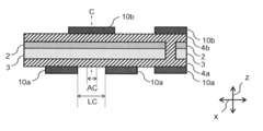
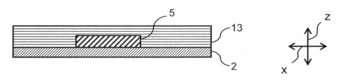
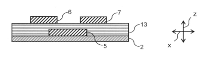
- FIG. 1 is a process sectional view of a method of manufacturing a thin film transistor according to an embodiment of the present invention.
- FIG. 2 is a process cross-sectional view of the thin film transistor manufacturing method according to the embodiment of the present invention.
- FIG. 3 is a process cross-sectional view of the method of manufacturing the thin film transistor according to the embodiment of the present invention.
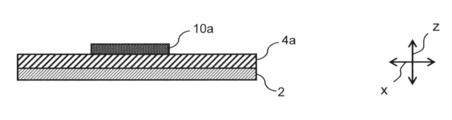
- FIG. 4 is a process sectional view of the method of manufacturing the thin film transistor according to the embodiment of the present invention.
- FIG. 5 is a process cross-sectional view of the thin film transistor manufacturing method according to the embodiment of the present invention.
- FIG. 6 is a process cross-sectional view of the method for manufacturing the thin film transistor according to the embodiment of the present invention.
- FIG. 1 is a process sectional view of a method of manufacturing a thin film transistor according to an embodiment of the present invention.
- FIG. 2 is a process cross-sectional view of the thin film transistor manufacturing method according to the embodiment of the present invention.
- FIG. 3 is a
- FIG. 7 is a process cross-sectional view of the method of manufacturing the thin film transistor according to the embodiment of the present invention.
- FIG. 8 is a process sectional view of the method of manufacturing the thin film transistor according to the embodiment of the present invention.
- FIG. 9 is a process cross-sectional view of the method of manufacturing the thin film transistor according to the embodiment of the present invention.
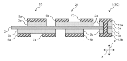
- FIG. 10 is a sectional view showing another example of the thin film transistor according to the embodiment of the present invention.
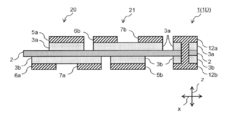
- FIG. 11 is a cross-sectional view showing another example of the thin film transistor according to the embodiment of the present invention.
- FIG. 12 is a schematic diagram showing a configuration of a CMOS circuit.
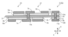
- FIG. 13 is a cross-sectional view showing another example of the thin film transistor according to the embodiment of the present invention.
- FIG. 14 is a process cross-sectional view of the method for manufacturing the thin film transistor according to the reference example.
- FIG. 15 is a process cross-sectional view of the method for manufacturing the thin film transistor according to the reference example.
- FIG. 16 is a process cross-sectional view of the method for manufacturing the thin film transistor according to the reference example.
- FIG. 17 is a process cross-sectional view of the method for manufacturing the thin film transistor according to the reference example.
- FIG. 18 is a process cross-sectional view of the method for manufacturing the thin film transistor according to the reference example.
- FIG. 19 is a process cross-sectional view of the manufacturing method of the thin film transistor according to the reference example.
- FIG. 20 is a process cross-sectional view of the method for manufacturing the thin film transistor according to the reference example.
- FIG. 21 is a process cross-sectional view of the manufacturing method of the thin film transistor according to the reference example.
- the method for producing a thin film transistor of the present invention includes (1) a step of forming an oxide semiconductor layer on one main surface of a substrate, and (2) forming a first conductive layer on the oxide semiconductor layer, A step of forming a second conductive layer on the other main surface, (3) a step of collectively forming a mask layer on the first conductive layer and the second conductive layer, and (4) a first conductive layer.
- Forming a source electrode and a drain electrode on the oxide semiconductor layer by bringing the first conductive layer and the second conductive layer into contact with an etching solution in a lump and removing a part of the first conductive layer and the second conductive layer.
- Forming a gate electrode on the other main surface of the substrate includes (1) a step of forming an oxide semiconductor layer on one main surface of a substrate, and (2) forming a first conductive layer on the oxide semiconductor layer, A step of forming a second conductive layer on the other main surface, (3) a step of collectively forming a mask layer on the first conductive
- the method for producing a thin film transistor of the present invention includes (3) a step of collectively forming a mask layer on the first conductive layer and the second conductive layer. It becomes easy to maintain the positional relationship between the source electrode, the drain electrode, and the gate electrode. As a result, it is possible to suppress degradation in the performance of the transistor due to the positional deviation of the gate electrode with respect to the source electrode and the drain electrode.
- the thin film transistor of the present invention includes a base material, an oxide semiconductor layer formed on one main surface of the base material, a source electrode formed on the oxide semiconductor layer, and an oxide semiconductor layer And a gate electrode formed on the other main surface of the substrate.
- the base material also serves as a gate insulating film, it is not necessary to separately provide a gate insulating film such as a silicon oxide film, and the thickness of the entire transistor can be suppressed. Further, there is no variation in transistor performance due to the occurrence of pinholes in the gate insulating film and variations in quality such as film thickness.
- the thin film transistor of the present invention includes a base material, a first oxide semiconductor layer formed on one main surface of the base material, and a second oxide formed on the other main surface of the base material.
- a transistor since the base material also serves as a gate insulating film, it is not necessary to separately provide a gate insulating film such as a silicon oxide film, and the thickness of the entire transistor can be suppressed.
- the thin film transistor of the present invention there is no variation in transistor performance due to the occurrence of pinholes in the gate insulating film and variations in quality such as film thickness.
- two transistors are arranged in different directions with a base material interposed therebetween. Therefore, the arrangement interval between adjacent transistors can be reduced, and the degree of circuit integration can be increased.
- the thin film transistor has a thickness direction and a plane direction.
- the thickness direction of the thin film transistor is a direction in which the oxide semiconductor layer and the conductive layer are stacked on the base material, and corresponds to the vertical direction in the drawing of the present application.
- the surface direction of the thin film transistor is a direction orthogonal to the thickness direction, and has a vertical direction and a horizontal direction. Note that the left-right direction in the drawing of the present application corresponds to the lateral direction of the surface direction of the thin film transistor.
- the base material also serves as a gate insulating film.
- the substrate is preferably formed from a polymer film such as polyethylene naphthalate (PEN), polyethylene terephthalate (PET), polyimide (PI), or the like.
- PEN polyethylene naphthalate
- PET polyethylene terephthalate
- PI polyimide
- the thickness of the substrate is preferably 0.1 ⁇ m or more and 50 ⁇ m or less, preferably 0.5 ⁇ m or more and 40 ⁇ m or less, and more preferably 1 ⁇ m or more and 30 ⁇ m or less.
- the oxide semiconductor layer functions as a channel region of the transistor.
- a ZnO-based, NiO-based, TiO-based, InO-based, SnO-based, InGaO-based, InZnO-based, InGaZnO-based (IGZO), or the like can be used as a material of the oxide semiconductor layer.
- the oxide semiconductor layer is preferably a layer containing In, Ga, Zn, and O (hereinafter referred to as “IGZO”). Since the electron mobility of IGZO is as high as 10 cm 2 / V ⁇ sec, the processing speed of the transistor can be improved.
- the first conductive layer and the second conductive layer are for forming respective electrodes such as a gate electrode, a source electrode, a drain electrode, a terminal electrode, and a via electrode constituting the transistor.
- electrodes such as a gate electrode, a source electrode, a drain electrode, a terminal electrode, and a via electrode constituting the transistor.
- the details will be described later with reference to an example of a manufacturing method.
- the first conductive layer and the second conductive layer for example, a conductive material such as Al, Ag, C, Ni, Au, or Cu can be used. Especially, it is preferable that the 1st conductive layer and the 2nd conductive layer are comprised from Cu. This is because Cu has high electrical conductivity, is inexpensive, and has excellent heat resistance.
- FIG. 1 to 9 are process cross-sectional views illustrating a part of the method of manufacturing the thin film transistor according to the present embodiment.
- Step of forming an oxide semiconductor layer on one main surface of the base material A polyimide film having a film thickness of 25 ⁇ m is prepared as the base material 2, and on one main surface of the base material 2, as shown in FIG. An oxide semiconductor layer 3 (for example, IGZO) is formed. In FIG. 1, the oxide semiconductor layer 3 is formed on the lower surface of the base material 2 in the thickness direction z.
- a method for forming the oxide semiconductor layer 3 is not particularly limited, and for example, a vacuum deposition method, a sputtering method, a method of attaching a conductive material formed in a foil shape, or the like can be used.
- a through hole 11a penetrating the base material 2 and the oxide semiconductor layer 3 in the thickness direction z is formed. Punching, laser processing, or the like can be used to form the through hole 11a.
- Step of forming a first conductive layer on the oxide semiconductor layer and forming a second conductive layer on the other main surface of the substrate Forming a first conductive layer 4a on the oxide semiconductor layer 3, A second conductive layer 4b is formed on the other main surface of the substrate 2. That is, as shown in FIG. 3, the first conductive layer 4 a is formed below the oxide semiconductor layer 3 in the thickness direction z, and the second conductive layer 4 b is formed above the substrate 2.
- a vacuum evaporation method or a sputtering method can be used as in the case of forming the oxide semiconductor layer 3 described above.
- Step of collectively forming a mask layer on the first conductive layer and the second conductive layer As shown in FIG. 4, a mask for determining the formation positions of the gate electrode, the source electrode, and the drain electrode
- the layers 10a and 10b are collectively formed on the first conductive layer 4a and the second conductive layer 4b, respectively.
- the mask layer 10 (10a, 10b) is formed as follows.
- a photosensitive resin such as a dry film resist or a liquid resist is applied on the first conductive layer 4a and the second conductive layer 4b.
- the photosensitive resin includes a negative type in which the exposed portion is insoluble in the developer and a positive type in which the exposed portion is soluble in the developer.
- a negative photosensitive resin is taken as an example. explain.
- a first resist is applied on the first conductive layer 4a, and a second resist is applied on the second conductive layer 4b.
- a predetermined circuit shape is drawn on the first resist and the second resist by irradiating an electron beam or light (ultraviolet rays) on the first resist and the second resist. At least the shape of the source electrode and the drain electrode is drawn on the first resist, and at least the shape of the gate electrode is drawn on the second resist.
- the center line C in the left-right direction x of the mask layer 10b for forming the gate electrode is between the source electrode and the drain electrode formed by the mask layer 10a.
- the region (channel length LC) is preferably located in the central region AC when it is divided into three equal parts in the left-right direction x.
- the channel length LC is preferably 20 ⁇ m or less, more preferably 15 ⁇ m or less, and even more preferably 10 ⁇ m or less. The shorter the channel length LC, the higher the transistor processing speed.
- both the first resist and the second resist are exposed at once, whereby the first resist and the second resist are exposed.
- the circuit shape is transferred and baked.
- the unexposed portion of each resist is dissolved in the developer.
- the exposed portions of the first resist and the second resist remain on the first conductive layer 4a and the second conductive layer 4b as the mask layers 10a and 10b.
- the mask layer 10 can be formed of a dry film resist or a liquid resist, but is preferably formed of a dry film resist. Compared with the case where the mask layer 10 is formed of a liquid resist, it is not necessary to dry the solvent after applying the resist, so that productivity can be improved.
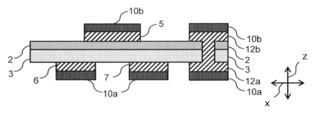
- a source electrode is formed on the oxide semiconductor layer by bringing the first conductive layer and the second conductive layer into contact with an etching solution in a lump and removing a part of the first conductive layer and the second conductive layer. Forming a drain electrode and forming a gate electrode on the other main surface of the substrate Next, a first conductive layer 4a on which a mask layer 10a is formed and a second conductive layer on which a mask layer 10b is formed 4b is brought into contact with the etching solution all at once. By this operation, as shown in FIG. 5, partial regions of the first conductive layer 4a and the second conductive layer 4b are removed.
- the mask layers 10a and 10b are removed by bringing the mask layers 10a and 10b into contact with a stripping solution and dissolving them.
- a thin film transistor in which the source electrode 6 and the drain electrode 7 are formed on the oxide semiconductor layer 3 and the gate electrode 5 is formed on the other main surface of the base 2 can be obtained.
- the source electrode 6, the drain electrode 7, and the gate electrode 5 are formed by collective photolithography and collective wet etching. For this reason, even if the base material 2 is thermally stretched or thermally contracted, the positional relationship among the source electrode 6, the drain electrode 7, and the gate electrode 5 can be easily maintained. As a result, the performance degradation of the thin film transistor due to the positional deviation of the gate electrode 5 with respect to the source electrode 6 and the drain electrode 7 can be suppressed.
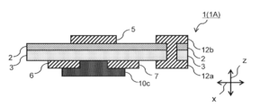
- the mask layer 10c is formed so as to cover the lower surface of the base material 2 in the thickness direction z.
- the mask layer 10c can be formed, for example, by printing a resist only on the channel region.
- the source electrode 6, the drain electrode 7, and the terminal electrode 12a function as a mask.
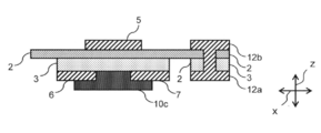
- the etching widths of the left end portion of the source electrode 6 and the left end portion of the oxide semiconductor layer 3 can be made uniform.
- the etching widths of the right end portion of the drain electrode 7 and the right end portion of the oxide semiconductor layer 3 can be made uniform.
- terminal electrodes 12 a and 12 b and via electrodes (not shown) can be formed on the substrate 2.
- the mask layer 10c is removed by bringing the mask layer 10c into contact with a stripping solution and dissolving it. Thereby, the thin film transistor 1 (1B) is manufactured.
- FIGS. 10 to 13 are cross-sectional views of the thin film transistor in the thickness direction z.
- a thin film transistor 1 (1C) of the present invention shown in FIG. 10 includes a base material 2, a first oxide semiconductor layer 3a formed on one main surface of the base material 2, and the other main surface of the base material 2.
- a second oxide semiconductor layer 3b formed on the first oxide semiconductor layer 3a; a first gate electrode 5a formed on the first oxide semiconductor layer 3a; and a second oxide semiconductor layer 3b.
- a first transistor 20 having a first source electrode 6a and a first drain electrode 7a; a second gate electrode 5b formed on the second oxide semiconductor layer 3b; and a first transistor 20 formed on the first oxide semiconductor layer 3a.
- the second transistor 21 having the second source electrode 6b and the second drain electrode 7b.
- the first gate electrode 5a of the first transistor 20 is formed between the first source electrode 6a and the first drain electrode 7a, and the second gate electrode 5b of the second transistor 21 is connected to the second source electrode 6b and the second source electrode 6b. It is formed between the two drain electrodes 7b.
- the second oxide semiconductor layer 3b in which the first source electrode 6a and the first drain electrode 7a are formed that contribute to the operation of the first transistor 20.
- the first oxide semiconductor layer 3a in which the second source electrode 6b and the second drain electrode 7b are formed contributes to the operation of the second transistor 21.
- the thin film transistor 1C of the present invention since two transistors are arranged in different directions with the base material 2 interposed therebetween, the arrangement interval between adjacent transistors can be reduced, and the degree of circuit integration is increased. It is what
- the first gate electrode 5a, the first source electrode 6a, the first drain electrode 7a, the second gate electrode 5b, the second source electrode 6b, and the second drain electrode 7b are batch photolithography and batch wet etching. It is preferable that it is formed by. Even if the substrate 2 is thermally stretched or contracted, the first gate electrode 5a, the first source electrode 6a, the first drain electrode 7a; the second gate electrode 5b, the second source electrode 6b, the second drain electrode 7b; It becomes easy to maintain each positional relationship.
- a plurality of transistors can be manufactured as in the case of manufacturing one transistor, so that productivity can be improved. it can.
- the first source electrode 6a or the first drain electrode 7a and the second source electrode 6b or the second drain electrode 7b are arranged to overlap each other.
- the arrangement interval between adjacent transistors can be further reduced.
- the first drain electrode 7a and the second source electrode 6b are arranged so as to overlap each other, but the first source electrode 6a and the second source electrode 6b are arranged in accordance with the semiconductor conductivity type and the circuit type.
- the two source electrodes 6b may be arranged to overlap each other, the first source electrode 6a and the second drain electrode 7b may be arranged to overlap each other, or the first drain electrode 7a and the second drain electrode 7b may overlap each other. May be arranged.
- the conductivity type of the first oxide semiconductor layer 3a and the conductivity type of the second oxide semiconductor layer 3b have opposite polarities, and the first transistor 20 and the second transistor 21 are configured to be complementary. Thereby, the first transistor 20 and the second transistor 21 can be arranged in a CMOS structure called a metal oxide semiconductor (MOS).
- MOS metal oxide semiconductor
- FIG. 12 is a schematic diagram showing the configuration of a CMOS circuit.
- a CMOS has a circuit configuration in which PMOS and NMOS are paired and the operation characteristics of the PMOS and NMOS are complementarily combined, and can be operated at a low voltage, so that power consumption can be suppressed.
- G represents a gate
- S represents a source
- D represents a drain
- IN represents an input
- OUT represents an output.
- the conductivity type of the first oxide semiconductor layer 3a and the conductivity type of the second oxide semiconductor layer 3b may have opposite polarities.
- the first oxide semiconductor layer 3a is p-type and the second oxide semiconductor layer 3b is n
- the first oxide semiconductor layer 3a may be n-type and the second oxide semiconductor layer 3b may be p-type.
- the first oxide semiconductor layer 3a and the second oxide semiconductor layer 3b are, for example, ZnO-based, NiO-based, TiO-based, InO-based, SnO-based, InGaO-based, and InZnO-based as in the above-described oxide semiconductor layer 3.
- InGaZnO (IGZO) or the like can be used.
- the 1st oxide semiconductor layer 3a or the 2nd oxide semiconductor layer 3b is what contains In, Ga, Zn, and O (IGZO). Since the electron mobility of IGZO is as high as 10 cm 2 / V ⁇ sec, the processing speed of the transistor can be improved.
- IGZO that operates as an n-type transistor can be used for the first oxide semiconductor layer 3a
- SnO that operates as a p-type transistor can be used for the second oxide semiconductor layer 3b.
- a thin film transistor can also be configured. That is, as shown in FIG. 13, the thin film transistor 1 (1E) is arranged in a region where the first drain electrode 7a and the second drain electrode 7b overlap each other and the first drain electrode 7a and the second drain electrode 7b overlap each other. It is preferable that a through hole 11b is formed in the thickness direction of the material 2 and the first drain electrode 7a and the second drain electrode 7b are connected through the through hole 11b. The through hole 11b is provided separately from the through hole 11a for conducting the terminal electrodes 12a and 12b.
- the arrangement interval between the first transistor 20 and the second transistor 21 in the horizontal direction x in FIG. 13 can be reduced.
- the wiring length for connecting the first drain electrode 5a and the second drain electrode can be shortened. There is no need to secure a separate space for Similar to the through hole 11a for forming the terminal electrode and the via electrode, the through hole 11b can be formed by punching, laser processing, or the like.
- FIGS. 14 to 21 are process cross-sectional views of a method of manufacturing a thin film transistor according to a reference example.
- the first conductive layer 4 a is formed on one main surface of the substrate 2.
- the first conductive layer 4a is formed by a vacuum deposition method or a sputtering method.
- a mask layer 10a for forming a gate electrode is formed on the first conductive layer 4a.
- the mask layer 10a is formed by, for example, applying and drying a photoresist on the first conductive layer 4a, transferring the circuit shape to the photoresist using an exposure device, and finally dissolving and removing unnecessary resist with a developer. Formed by.
- the first conductive layer 4a is etched using an etchant.
- the mask layer 10a is peeled and removed by bringing the mask layer 10a into contact with a stripping solution and dissolving it. Thereby, as shown in FIG. 16, the gate electrode 5 is formed on one main surface of the substrate 2.
- a gate insulating film 13 is formed on one main surface of the substrate 2 and the gate electrode 5.
- the gate insulating film 13 can be formed by using, for example, a spin coating method, a vacuum deposition method, or a sputtering method.
- a coating method such as a screen printing method or a gravure coater method is used.
- a die coating method or a spray method can be used.
- the second conductive layer 4 b is formed on the gate insulating film 13.
- a vacuum deposition method or a sputtering method can be used similarly to the formation of the first conductive layer 4a.
- a mask layer 10b for forming a source electrode and a drain electrode is formed on the second conductive layer 4b.
- the mask layer 10b is formed by applying and drying a photoresist on the second conductive layer 4b, transferring the circuit shape to the photoresist using an exposure apparatus, and finally removing unnecessary resist with a developer. It can be formed by dissolving and removing.
- the second conductive layer 4b is etched using an etchant.
- the mask layer 10b is peeled and removed by bringing the mask layer 10b into contact with the stripping solution and dissolving it. Thereby, as shown in FIG. 20, the source electrode 6 and the drain electrode 7 are formed on the gate insulating film 13.
- the oxide semiconductor layer 3 is formed on the same surface as the source electrode 6 and the drain electrode 7 of the gate insulating film 13.
- a vacuum vapor deposition method can be used for forming the oxide semiconductor layer 3.
- the stacking order and the manufacturing method of the thin film transistors according to the reference example are the mask layer 10a for forming the gate electrode 5, and the mask layer for forming the source electrode 6 and the drain electrode 7.
- the formation of 10b since exposure processing and the like are respectively performed, exposure is performed with the alignment mark as a reference.
- the alignment accuracy of the apparatus is easily accumulated and the base material is thermally stretched or contracted, the gate electrode is exposed. It is difficult to control the formation positions of the source electrode and the drain electrode.
Landscapes
- Thin Film Transistor (AREA)
- Electrodes Of Semiconductors (AREA)
Abstract
Description
本発明の薄膜トランジスタの製造方法および薄膜トランジスタは、基材がゲート絶縁膜を兼ねているため、シリコン酸化膜等のゲート絶縁膜を別途設ける必要がなく、トランジスタ全体の厚みを抑えることができる。これにより、ゲート絶縁膜のピンホールの発生や膜厚などの品質のバラツキに起因するトランジスタの性能のバラツキが発生しない。
さらに、第1トランジスタおよび第2トランジスタを含む本発明の薄膜トランジスタは基材を挟んで互いに異なる向きに2つのトランジスタが配置されているため、隣り合うトランジスタ同士の配置間隔を狭めることができ、回路の集積度を高められる。
膜厚25μmのポリイミドフィルムを基材2として準備し、図1に示すように、基材2の一方の主面上に酸化物半導体層3(例えばIGZO)を形成する。図1においては、基材2の厚み方向zの下側の面上に酸化物半導体層3が形成されている。酸化物半導体層3を成膜する方法は特に限定されず、例えば、真空蒸着法、スパッタリング法、箔状に形成された導電性材料を貼り付ける方法等を用いることができる。
酸化物半導体層3上に第1導電層4aを形成し、基材2の他方の主面上に第2導電層4bを形成する。すなわち、図3に示すように、厚み方向zにおいて酸化物半導体層3の下側に第1導電層4aが形成され、基材2の上側に第2導電層4bが形成される。第1導電層4aと第2導電層4bの形成方法は、上述した酸化物半導体層3の成膜と同様に、例えば、真空蒸着法やスパッタリング法を用いることができる。
図4に示すように、ゲート電極、ソース電極、ドレイン電極の各電極の形成位置を決めるためのマスク層10a、10bをそれぞれ第1導電層4a、第2導電層4bの上に一括して形成する。
ためのマスク層10bの左右方向xにおける中心線Cが、マスク層10aが形成するソー
ス電極とドレイン電極の間の領域(チャネル長LC)を左右方向xに三等分割した場合の
中央領域ACに位置していることが好ましい。
次に、マスク層10aが形成された第1導電層4aと、マスク層10bが形成された第2導電層4bを一括してエッチング液に接触させる。この操作によって、図5に示すように、第1導電層4aおよび第2導電層4bの一部領域が除去される。
図7に示すように、チャネル領域として機能する酸化物半導体層3の一部の領域がエッチングされるのを防ぐために、基材2の厚み方向zの下側面を覆うようにマスク層10cを形成する。マスク層10cの形成は、例えばチャネル領域のみにレジストを印刷することにより行うことができる。このように形成されたマスク層10cに加えて、ソース電極6、ドレイン電極7、端子電極12aがマスクとして機能する。
図8に示すように、酸化物半導体層3をエッチング液に接触させて、マスク層10cとソース電極6およびドレイン電極7に覆われていない酸化物半導体層3の領域を除去する。これにより、左右方向xにおいて、ソース電極6の左側端部と酸化物半導体層3の左側端部のエッチング幅を揃えることができる。また、左右方向xにおいて、ドレイン電極7の右側端部と酸化物半導体層3の右側端部のエッチング幅を揃えることができる。これにより、ソース電極6、ドレイン電極7とは別に、基材2上に端子電極12a、12bやビア電極(図示されていない)を形成することができる。
参考として、基材の一方の主面上に各層を形成する場合の薄膜トランジスタの製造方法について、図14~図21を用いて説明する。図14~図21は、参考例にかかる薄膜トランジスタの製造方法の工程断面図である。図14には、基材2の一方の主面上に第1導電層4aが形成されている。第1導電層4aの形成は、真空蒸着法やスパッタリング法によって行われる。
2:基材
3:酸化物半導体層
3a:第1酸化物半導体層
3b:第2酸化物半導体層
4a:第1導電層
4b:第2導電層
5:ゲート電極
5a:第1ゲート電極
5b:第2ゲート電極
6:ソース電極
6a:第1ソース電極
6b:第2ソース電極
7:ドレイン電極
7a:第1ドレイン電極
7b:第2ドレイン電極
8:ソース・ドレイン電極
10、10a、10b、10c:マスク層
11a、11b:貫通孔
12a、12b:端子電極
20:第1トランジスタ
21:第2トランジスタ
Claims (14)
- 基材の一方の主面上に酸化物半導体層を形成する工程と、
前記酸化物半導体層上に第1導電層を形成し、前記基材の他方の主面上に第2導電層を形成する工程と、
前記第1導電層および前記第2導電層の上にマスク層を一括して形成する工程と、
前記第1導電層と前記第2導電層を一括してエッチング液に接触させて、前記第1導電層および前記第2導電層の一部領域を除去することにより、前記酸化物半導体層上にソース電極とドレイン電極を形成し、前記基材の他方の主面上にゲート電極を形成する工程と、を含むことを特徴とする薄膜トランジスタの製造方法。 - 前記ソース電極および前記ドレイン電極を形成した後、該ソース電極および前記ドレイン電極の間を覆うようにマスク層を形成する工程と、
前記酸化物半導体層をエッチング液に接触させて、前記ソース電極、前記ドレイン電極およびマスク層に覆われていない前記酸化物半導体層の領域を除去する工程と、をさらに含む請求項1に記載の薄膜トランジスタの製造方法。 - 前記酸化物半導体層がIn、Ga、Zn、およびOを含むものである請求項1または2に記載の薄膜トランジスタの製造方法。
- 前記第1導電層および前記第2導電層が、Cuから構成されている請求項1~3のいずれか一項に記載の薄膜トランジスタの製造方法。
- 前記マスク層がドライフィルムレジストで形成されている請求項1~4のいずれか一項に記載の薄膜トランジスタの製造方法。
- 基材と、
該基材の一方の主面上に形成されている酸化物半導体層と、
前記酸化物半導体層上に形成されているソース電極と、
前記酸化物半導体層上に形成されているドレイン電極と、
前記基材の他方の主面上に形成されているゲート電極と、を有していることを特徴とする薄膜トランジスタ。 - 前記酸化物半導体層がIn、Ga、Zn、およびOとを含むものである請求項6に記載の薄膜トランジスタ。
- 前記ソース電極と、前記ドレイン電極と、前記ゲート電極が一括したフォトリソグラフィおよび一括したウェットエッチングにより形成されている請求項6または7に記載の薄膜トランジスタ。
- 基材と、
該基材の一方の主面上に形成されている第1酸化物半導体層と、
前基材の他方の主面上に形成されている第2酸化物半導体層と、を有する薄膜トランジスタであって、
前記第1酸化物半導体層上に形成されている第1ゲート電極と、
前記第2酸化物半導体層上に形成されている第1ソース電極と第1ドレイン電極を有する第1トランジスタと;
前記第2酸化物半導体層上に形成されている第2ゲート電極と、
前記第1酸化物半導体層上に形成されている第2ソース電極と第2ドレイン電極を有する第2トランジスタと;を含むことを特徴とする薄膜トランジスタ。 - 前記第1ソース電極または前記第1ドレイン電極と、前記第2ソース電極または前記第2ドレイン電極が重なって配置されている請求項9に記載の薄膜トランジスタ。
- 前記第1酸化物半導体層の導電型と前記第2酸化物半導体層の導電型とは反対極性であり、前記第1トランジスタと前記第2トランジスタは相補型に構成されている請求項9または10に記載の薄膜トランジスタ。
- 前記第1ドレイン電極と前記第2ドレイン電極が重なって配置され、前記第1ドレイン電極と前記第2ドレイン電極が重なる領域において、前記基材に貫通孔が形成されており、該貫通孔を通じて前記第1ドレイン電極と前記第2ドレイン電極が接続されている請求項11に記載の薄膜トランジスタ。
- 前記第1酸化物半導体層または前記第2酸化物半導体層がIn、Ga、Zn、およびOを含むものである請求項9~12のいずれか一項に記載の薄膜トランジスタ。
- 前記基材が高分子フィルムから形成されており、前記基材の厚みが0.1μm以上50μm以下である請求項6~13のいずれか一項に記載の薄膜トランジスタ。
Priority Applications (4)
| Application Number | Priority Date | Filing Date | Title |
|---|---|---|---|
| US15/558,673 US20180114862A1 (en) | 2015-03-30 | 2016-03-02 | Method for producing thin film transistor, and thin film transistor |
| KR1020177025251A KR20170133337A (ko) | 2015-03-30 | 2016-03-02 | 박막 트랜지스터의 제조 방법, 및 박막 트랜지스터 |
| CN201680015615.9A CN107408509A (zh) | 2015-03-30 | 2016-03-02 | 薄膜晶体管的制造方法以及薄膜晶体管 |
| DE112016000485.0T DE112016000485T5 (de) | 2015-03-30 | 2016-03-02 | Verfahren zum Herstellen eines Dünnfilmtransistors und Dünnfilmtransistor |
Applications Claiming Priority (2)
| Application Number | Priority Date | Filing Date | Title |
|---|---|---|---|
| JP2015070347A JP6050414B2 (ja) | 2015-03-30 | 2015-03-30 | 薄膜トランジスタの製造方法、および薄膜トランジスタ |
| JP2015-070347 | 2015-03-30 |
Publications (1)
| Publication Number | Publication Date |
|---|---|
| WO2016158180A1 true WO2016158180A1 (ja) | 2016-10-06 |
Family
ID=57004229
Family Applications (1)
| Application Number | Title | Priority Date | Filing Date |
|---|---|---|---|
| PCT/JP2016/056477 Ceased WO2016158180A1 (ja) | 2015-03-30 | 2016-03-02 | 薄膜トランジスタの製造方法、および薄膜トランジスタ |
Country Status (7)
| Country | Link |
|---|---|
| US (1) | US20180114862A1 (ja) |
| JP (1) | JP6050414B2 (ja) |
| KR (1) | KR20170133337A (ja) |
| CN (1) | CN107408509A (ja) |
| DE (1) | DE112016000485T5 (ja) |
| TW (1) | TW201705304A (ja) |
| WO (1) | WO2016158180A1 (ja) |
Families Citing this family (1)
| Publication number | Priority date | Publication date | Assignee | Title |
|---|---|---|---|---|
| WO2023233760A1 (ja) * | 2022-05-31 | 2023-12-07 | キヤノン株式会社 | 発光装置、表示装置、光電変換装置、電子機器、および、発光装置の製造方法 |
Citations (3)
| Publication number | Priority date | Publication date | Assignee | Title |
|---|---|---|---|---|
| WO2010058541A1 (ja) * | 2008-11-18 | 2010-05-27 | パナソニック株式会社 | フレキシブル半導体装置およびその製造方法 |
| WO2010134234A1 (ja) * | 2009-05-19 | 2010-11-25 | パナソニック株式会社 | フレキシブル半導体装置の製造方法 |
| WO2012127779A1 (ja) * | 2011-03-24 | 2012-09-27 | パナソニック株式会社 | フレキシブル半導体装置及びその製造方法 |
Family Cites Families (2)
| Publication number | Priority date | Publication date | Assignee | Title |
|---|---|---|---|---|
| CN100437948C (zh) * | 2007-02-07 | 2008-11-26 | 友达光电股份有限公司 | 薄膜晶体管及半导体元件的制作方法 |
| KR100958006B1 (ko) * | 2008-06-18 | 2010-05-17 | 삼성모바일디스플레이주식회사 | 박막 트랜지스터, 그의 제조 방법 및 박막 트랜지스터를구비하는 평판 표시 장치 |
-
2015
- 2015-03-30 JP JP2015070347A patent/JP6050414B2/ja not_active Expired - Fee Related
-
2016
- 2016-03-02 WO PCT/JP2016/056477 patent/WO2016158180A1/ja not_active Ceased
- 2016-03-02 KR KR1020177025251A patent/KR20170133337A/ko not_active Withdrawn
- 2016-03-02 DE DE112016000485.0T patent/DE112016000485T5/de not_active Withdrawn
- 2016-03-02 CN CN201680015615.9A patent/CN107408509A/zh active Pending
- 2016-03-02 US US15/558,673 patent/US20180114862A1/en not_active Abandoned
- 2016-03-04 TW TW105106703A patent/TW201705304A/zh unknown
Patent Citations (3)
| Publication number | Priority date | Publication date | Assignee | Title |
|---|---|---|---|---|
| WO2010058541A1 (ja) * | 2008-11-18 | 2010-05-27 | パナソニック株式会社 | フレキシブル半導体装置およびその製造方法 |
| WO2010134234A1 (ja) * | 2009-05-19 | 2010-11-25 | パナソニック株式会社 | フレキシブル半導体装置の製造方法 |
| WO2012127779A1 (ja) * | 2011-03-24 | 2012-09-27 | パナソニック株式会社 | フレキシブル半導体装置及びその製造方法 |
Also Published As
| Publication number | Publication date |
|---|---|
| TW201705304A (zh) | 2017-02-01 |
| JP2016192437A (ja) | 2016-11-10 |
| DE112016000485T5 (de) | 2017-11-02 |
| JP6050414B2 (ja) | 2016-12-21 |
| KR20170133337A (ko) | 2017-12-05 |
| CN107408509A (zh) | 2017-11-28 |
| US20180114862A1 (en) | 2018-04-26 |
Similar Documents
| Publication | Publication Date | Title |
|---|---|---|
| CN103715196B (zh) | 一种阵列基板及其制作方法、显示装置 | |
| CN104779272B (zh) | 薄膜晶体管和阵列基板及其制作方法、显示装置 | |
| US9536751B2 (en) | Method for forming patterns for semiconductor device | |
| JP6437574B2 (ja) | 薄膜トランジスタおよびその製造方法、アレイ基板、並びに表示装置 | |
| US7939828B2 (en) | Pixel structure and method for fabricating the same | |
| JPWO2016175086A1 (ja) | 半導体装置及びその製造方法 | |
| CN107706198A (zh) | 阵列基板及其制造方法 | |
| KR101415484B1 (ko) | 유기 tft 어레이 기판 및 그 제조 방법 | |
| KR20140041403A (ko) | 유기 박막 트랜지스터 어레이 기판 및 그 제조 방법, 및 디스플레이 장치 | |
| KR100307459B1 (ko) | 박막트랜지스터 제조방법 | |
| US9741861B2 (en) | Display device and method for manufacturing the same | |
| JP6005204B1 (ja) | 薄膜トランジスタの製造方法、および薄膜トランジスタ | |
| JP6050414B2 (ja) | 薄膜トランジスタの製造方法、および薄膜トランジスタ | |
| US9806109B2 (en) | Half tone mask plate and method for manufacturing array substrate using the same | |
| US9859308B1 (en) | Multiple TFTs on common vertical support element | |
| US10074651B2 (en) | Semiconductor device having transistors formed by double patterning and manufacturing method therefor | |
| US9257423B2 (en) | Method to provide the thinnest and variable substrate thickness for reliable plastic and flexible electronic device | |
| CN106373888A (zh) | 薄膜晶体管的制造方法 | |
| TWI662709B (zh) | 電子元件及其製作方法 | |
| JP6555843B2 (ja) | アレイ基板及びその製造方法 | |
| CN108598040A (zh) | 阵列基板及其制造方法、驱动晶体管、显示面板 | |
| CN108321122B (zh) | Cmos薄膜晶体管及其制备方法和显示装置 | |
| TWI735675B (zh) | 半導體元件及其製作方法 | |
| US11145648B2 (en) | Enhancement/depletion device pairs and methods of producing the same | |
| WO2020037724A1 (zh) | 阵列基板及其制作方法 |
Legal Events
| Date | Code | Title | Description |
|---|---|---|---|
| 121 | Ep: the epo has been informed by wipo that ep was designated in this application |
Ref document number: 16772064 Country of ref document: EP Kind code of ref document: A1 |
|
| WWE | Wipo information: entry into national phase |
Ref document number: 112016000485 Country of ref document: DE |
|
| ENP | Entry into the national phase |
Ref document number: 20177025251 Country of ref document: KR Kind code of ref document: A |
|
| WWE | Wipo information: entry into national phase |
Ref document number: 15558673 Country of ref document: US |
|
| 122 | Ep: pct application non-entry in european phase |
Ref document number: 16772064 Country of ref document: EP Kind code of ref document: A1 |