WO2016157697A1 - 露光装置及び露光方法 - Google Patents
露光装置及び露光方法 Download PDFInfo
- Publication number
- WO2016157697A1 WO2016157697A1 PCT/JP2016/000908 JP2016000908W WO2016157697A1 WO 2016157697 A1 WO2016157697 A1 WO 2016157697A1 JP 2016000908 W JP2016000908 W JP 2016000908W WO 2016157697 A1 WO2016157697 A1 WO 2016157697A1
- Authority
- WO
- WIPO (PCT)
- Prior art keywords
- light
- optical system
- dmd
- imaging optical
- exposure
- Prior art date
- Legal status (The legal status is an assumption and is not a legal conclusion. Google has not performed a legal analysis and makes no representation as to the accuracy of the status listed.)
- Ceased
Links
Images





Classifications
-
- G—PHYSICS
- G03—PHOTOGRAPHY; CINEMATOGRAPHY; ANALOGOUS TECHNIQUES USING WAVES OTHER THAN OPTICAL WAVES; ELECTROGRAPHY; HOLOGRAPHY
- G03F—PHOTOMECHANICAL PRODUCTION OF TEXTURED OR PATTERNED SURFACES, e.g. FOR PRINTING, FOR PROCESSING OF SEMICONDUCTOR DEVICES; MATERIALS THEREFOR; ORIGINALS THEREFOR; APPARATUS SPECIALLY ADAPTED THEREFOR
- G03F7/00—Photomechanical, e.g. photolithographic, production of textured or patterned surfaces, e.g. printing surfaces; Materials therefor, e.g. comprising photoresists; Apparatus specially adapted therefor
- G03F7/70—Microphotolithographic exposure; Apparatus therefor
- G03F7/70058—Mask illumination systems
- G03F7/70091—Illumination settings, i.e. intensity distribution in the pupil plane or angular distribution in the field plane; On-axis or off-axis settings, e.g. annular, dipole or quadrupole settings; Partial coherence control, i.e. sigma or numerical aperture [NA]
- G03F7/70116—Off-axis setting using a programmable means, e.g. liquid crystal display [LCD], digital micromirror device [DMD] or pupil facets
-
- G—PHYSICS
- G02—OPTICS
- G02B—OPTICAL ELEMENTS, SYSTEMS OR APPARATUS
- G02B3/00—Simple or compound lenses
-
- G—PHYSICS
- G02—OPTICS
- G02B—OPTICAL ELEMENTS, SYSTEMS OR APPARATUS
- G02B19/00—Condensers, e.g. light collectors or similar non-imaging optics
-
- G—PHYSICS
- G02—OPTICS
- G02B—OPTICAL ELEMENTS, SYSTEMS OR APPARATUS
- G02B26/00—Optical devices or arrangements for the control of light using movable or deformable optical elements
- G02B26/02—Optical devices or arrangements for the control of light using movable or deformable optical elements for controlling the intensity of light
-
- G—PHYSICS
- G03—PHOTOGRAPHY; CINEMATOGRAPHY; ANALOGOUS TECHNIQUES USING WAVES OTHER THAN OPTICAL WAVES; ELECTROGRAPHY; HOLOGRAPHY
- G03F—PHOTOMECHANICAL PRODUCTION OF TEXTURED OR PATTERNED SURFACES, e.g. FOR PRINTING, FOR PROCESSING OF SEMICONDUCTOR DEVICES; MATERIALS THEREFOR; ORIGINALS THEREFOR; APPARATUS SPECIALLY ADAPTED THEREFOR
- G03F7/00—Photomechanical, e.g. photolithographic, production of textured or patterned surfaces, e.g. printing surfaces; Materials therefor, e.g. comprising photoresists; Apparatus specially adapted therefor
- G03F7/20—Exposure; Apparatus therefor
-
- G—PHYSICS
- G03—PHOTOGRAPHY; CINEMATOGRAPHY; ANALOGOUS TECHNIQUES USING WAVES OTHER THAN OPTICAL WAVES; ELECTROGRAPHY; HOLOGRAPHY
- G03F—PHOTOMECHANICAL PRODUCTION OF TEXTURED OR PATTERNED SURFACES, e.g. FOR PRINTING, FOR PROCESSING OF SEMICONDUCTOR DEVICES; MATERIALS THEREFOR; ORIGINALS THEREFOR; APPARATUS SPECIALLY ADAPTED THEREFOR
- G03F7/00—Photomechanical, e.g. photolithographic, production of textured or patterned surfaces, e.g. printing surfaces; Materials therefor, e.g. comprising photoresists; Apparatus specially adapted therefor
- G03F7/70—Microphotolithographic exposure; Apparatus therefor
- G03F7/70216—Mask projection systems
- G03F7/70241—Optical aspects of refractive lens systems, i.e. comprising only refractive elements
-
- G—PHYSICS
- G03—PHOTOGRAPHY; CINEMATOGRAPHY; ANALOGOUS TECHNIQUES USING WAVES OTHER THAN OPTICAL WAVES; ELECTROGRAPHY; HOLOGRAPHY
- G03F—PHOTOMECHANICAL PRODUCTION OF TEXTURED OR PATTERNED SURFACES, e.g. FOR PRINTING, FOR PROCESSING OF SEMICONDUCTOR DEVICES; MATERIALS THEREFOR; ORIGINALS THEREFOR; APPARATUS SPECIALLY ADAPTED THEREFOR
- G03F7/00—Photomechanical, e.g. photolithographic, production of textured or patterned surfaces, e.g. printing surfaces; Materials therefor, e.g. comprising photoresists; Apparatus specially adapted therefor
- G03F7/70—Microphotolithographic exposure; Apparatus therefor
- G03F7/70216—Mask projection systems
- G03F7/70275—Multiple projection paths, e.g. array of projection systems, microlens projection systems or tandem projection systems
-
- G—PHYSICS
- G03—PHOTOGRAPHY; CINEMATOGRAPHY; ANALOGOUS TECHNIQUES USING WAVES OTHER THAN OPTICAL WAVES; ELECTROGRAPHY; HOLOGRAPHY
- G03F—PHOTOMECHANICAL PRODUCTION OF TEXTURED OR PATTERNED SURFACES, e.g. FOR PRINTING, FOR PROCESSING OF SEMICONDUCTOR DEVICES; MATERIALS THEREFOR; ORIGINALS THEREFOR; APPARATUS SPECIALLY ADAPTED THEREFOR
- G03F7/00—Photomechanical, e.g. photolithographic, production of textured or patterned surfaces, e.g. printing surfaces; Materials therefor, e.g. comprising photoresists; Apparatus specially adapted therefor
- G03F7/70—Microphotolithographic exposure; Apparatus therefor
- G03F7/708—Construction of apparatus, e.g. environment aspects, hygiene aspects or materials
- G03F7/70808—Construction details, e.g. housing, load-lock, seals or windows for passing light in or out of apparatus
- G03F7/70833—Mounting of optical systems, e.g. mounting of illumination system, projection system or stage systems on base-plate or ground
Definitions
- the present invention relates to an exposure apparatus and an exposure method for passing light modulated by a spatial light modulation element through an imaging optical system and forming an image of this light on a predetermined surface.
- the DI exposure apparatus includes a plurality of exposure heads having a spatial light modulator (DMD), a first projection optical system, a microlens array (MLA), and a second projection optical system.
- DMD Digital Micromirror Device
- MLA microlens array
- the DI exposure apparatus projects light modulated by DMD onto the MLA by the first projection lens, and projects light transmitted through the MLA onto a predetermined light irradiation surface by the second projection lens.
- the MLA is a lens in which microlenses corresponding to the respective pixel portions of the DMD are arranged in an array in accordance with the positions of the respective pixels of the DMD.
- Patent Document 1 Japanese Patent Laid-Open No. 2001-305663
- light from a light source is irradiated on the entire surface of the DMD.
- the DMD has a configuration in which micromirrors (micromirrors) are two-dimensionally arranged, and there are microscopic gaps between adjacent micromirrors. Therefore, when light is irradiated on the entire surface of the DMD, the gap is also irradiated with light.
- the light applied to the gaps between the micromirrors does not contribute to the spatial modulation, causing a reduction in element efficiency.
- light from the light source for example, ultraviolet light (UV light) is used.
- UV light ultraviolet light
- an object of the present invention is to provide an exposure apparatus and an exposure method that can improve the efficiency and life of the spatial light modulator.
- an aspect of the exposure apparatus includes a microlens array in which microlenses that collect light from a light source are arranged in an array, and the microlens array that collects the light.
- a spatial light modulation unit in which pixel units for modulating light are arranged; a first imaging optical system that forms an image of the light collected by the microlens array on the spatial light modulation unit; and the spatial light modulation unit
- a second image-forming optical system that forms an image on the photosensitive material.
- the light condensed by the MLA can enter the spatial light modulator without loss. Therefore, the efficiency of spatial modulation can be improved. Further, the light condensed by the MLA is not irradiated onto, for example, the substrate of the spatial light modulator that does not contribute to the spatial modulation. Therefore, the deterioration of the element can be suppressed and the life can be extended.
- the spatial light modulation unit may be a digital micromirror device
- the pixel unit may be a micromirror that has a one-to-one correspondence with the microlens.
- DMD digital micromirror device
- the DMD micromirrors are made to correspond one-to-one with the MLA microlens, and the light collected by the MLA is imaged on the DMD micromirror, thereby suppressing crosstalk between pixels and reducing the extinction ratio. Can be suppressed.
- the first imaging optical system is configured to apply spot-like light collected by each microlens of the microlens array onto the corresponding micromirror. You may image with a spot size smaller than the size of. In this way, since light having a spot size smaller than the size of the micromirror is imaged on the micromirror, it is possible to reliably prevent light from entering the gap formed between the micromirrors. .
- the second imaging optical system may be an enlarged imaging optical system. In this way, by adopting a configuration in which the light modulated by the spatial light modulator is enlarged and imaged on the photosensitive material, the resolution requirement can be appropriately satisfied by adjusting the magnification. Further, the image can be enlarged while keeping the sharpness of the image projected on the photosensitive material high.
- the first imaging optical system may be a reduction imaging optical system.
- the first imaging optical system may be a reduction imaging optical system.
- the MLA by reducing the light collected by the MLA and forming an image on the spatial light modulation unit, it is possible to employ an MLA having a relatively large condensing spot size. Therefore, manufacture of MLA becomes easy.
- light from a light source is collected by a microlens array in which microlenses are arranged in an array, and light collected by the microlens array is arranged in a pixel unit. The light is imaged on the spatial light modulation unit, and the light modulated by the spatial light modulation unit is imaged on the photosensitive material.
- the light condensed by the MLA can be incident on the spatial light modulator without loss, and the efficiency of spatial modulation can be improved.
- the light collected by the MLA is not irradiated onto, for example, the substrate of the spatial light modulation unit that does not contribute to the spatial modulation, the deterioration of the element can be suppressed and the life can be extended.
- the light condensed by the microlens array can be incident on the spatial light modulator without loss. Therefore, it is possible to improve the efficiency and extend the life of the spatial light modulator.
- FIG. 1 is a schematic block diagram that shows the exposure apparatus of the present embodiment.
- FIG. 2 is a view showing the main part of the exposure head unit.
- FIG. 3 is a partially enlarged view showing the structure of the DMD.
- FIG. 4 is a perspective view showing a schematic configuration of the exposure head.
- FIG. 5 is an optical arrangement diagram showing the configuration of the exposure head.
- FIG. 6 is a diagram illustrating a state of a spot irradiated on the DMD surface.
- FIG. 7 is an optical arrangement diagram showing a configuration of a conventional exposure head.
- FIG. 8 is a diagram illustrating a state of light irradiated on a conventional DMD surface.
- FIG. 9 is a diagram showing a configuration of a conventional MLA surface.
- FIG. 1 is a schematic block diagram that shows the exposure apparatus of the present embodiment.
- the exposure apparatus 100 is an apparatus that exposes light that has been modulated by a spatial light modulation unit (spatial light modulation element) through an imaging optical system, and forms an image of the light on a photosensitive material (resist). Since such an exposure apparatus directly forms an image with a spatial light modulation element, no mask (or reticle) is required, and it is called a DI (direct image) exposure apparatus.
- a spatial light modulation unit spatial light modulation element
- DI direct image
- the exposure apparatus 100 includes an exposure head unit 10, a transport system 20 that transports a substrate (workpiece) W to be exposed, and a thick plate-shaped installation base 30 on which the exposure head unit 10 and the transport system 20 are installed.
- the workpiece W is, for example, a resin printed board coated with a resist.
- the exposure head unit 10 is fixed to a gate-like gate (gantry) 31 provided so as to straddle the installation table 30, and each end of the gate 31 is fixed to a side surface of the installation table 30. Further, the installation table 30 is supported by a plurality of (for example, four) leg portions 32.
- the transport system 20 includes, as an example, a flat plate-like stage 21 that sucks and holds the workpiece W by a method such as vacuum suction, two guides 22 that extend along the moving direction of the stage 21, and a moving mechanism of the stage 21. And an electromagnet 23.
- a linear motor stage is employed as the moving mechanism.
- a moving body (stage) is levitated by air on a flat platen provided with ferromagnetic convex poles in a lattice shape, and a magnetic force is applied to the moving body, so that the moving body and the platen
- This is a mechanism for moving the moving body (stage) by changing the magnetic force between the convex poles.
- the moving mechanism for example, a mechanism using a ball screw can be adopted.
- the stage 21 is arranged so that its longitudinal direction is directed to the stage moving direction, and is supported by the guide 22 so as to be able to reciprocate in a state where straightness is compensated.
- the moving direction of the stage 21 is defined as the X direction
- the horizontal direction perpendicular to the X direction is defined as the Y direction
- the vertical direction is defined as the Z direction.
- the workpiece W has a square shape and is held on the stage 21 in a posture in which one side is directed in the X direction and the other side is directed in the Y direction.
- the X direction may be referred to as the length direction of the workpiece W
- the Y direction may be referred to as the width direction of the workpiece W.
- the moving path of the stage 21 is designed to pass directly under the exposure head unit 10, and the transport system 20 transports the workpiece W to a light irradiation position by the exposure head unit 10 and passes the irradiation position. It is configured as follows. In the process of passing, the pattern of the image formed by the exposure head unit 10 is exposed on the workpiece W.
- the exposure head unit 10 is provided on one side of the gate 31 in the X direction, and a plurality of (for example, two) sensors 40 for detecting the front and rear ends of the workpiece W are provided on the other side. That is, the gate 31 provided with the exposure head unit 10 and the sensor 40 is fixedly arranged upstream of the moving path of the stage 21.
- the exposure head unit 10 and the sensor 40 are connected to a controller (not shown) that controls them.
- the exposure head unit 10 includes a plurality of (14 in FIG. 2) exposure heads 11 arranged in a substantially matrix of m rows and n columns. Each exposure head 11 incorporates the spatial light modulation element described above and irradiates light with a preset pattern.
- An exposure area 51 by each exposure head 11 has a rectangular shape with a short side in the sub-scanning direction. Accordingly, as the stage 21 moves, a strip-shaped exposed area 52 is formed on the work W for each exposure head 11.
- a digital micromirror device (DMD) 12 shown in FIG. 3 is used as the spatial light modulation element.
- the DMD 12 has a configuration in which fine mirrors (micromirrors) 122 of about 13 ⁇ m square that constitute each pixel (pixel) are two-dimensionally arranged on a memory cell (for example, SRAM cell) 121.
- the number of micromirrors 122 arranged is, for example, 1024 ⁇ 768.
- a rectangular micromirror 122 supported by a support column is provided at the top, and a material having a high reflectance such as aluminum is deposited on the surface of the micromirror 122. Note that a minute gap of 1 ⁇ m or less exists between adjacent micromirrors 122.
- each micromirror 122 supported by the support is tilted to any one of ⁇ ⁇ degrees with respect to the substrate side on which the DMD 12 is disposed with the diagonal line as the center.
- the controller controls the angle of each micromirror 122 of the DMD 12 so as to form a desired pattern on the workpiece W. That is, the angle of each micro mirror 122 of the DMD 12 is selectively controlled according to the pattern of the image to be formed.
- the exposure head 11 includes a light source unit 13, an incident optical system 14, and a mirror 15 on the light incident side of the DMD 12.
- the light source unit 13 includes a light source such as a lamp that emits laser light having a wavelength of 400 nm and a semiconductor laser (laser diode).
- the light source unit 13 includes an optical fiber that guides output light from the light source.
- the optical fiber for example, a quartz fiber can be used.
- the emission end portions (light emission points) of the optical fiber are arranged in a line along a direction corresponding to the long side direction of the exposure area 51 to constitute a laser emission unit 131.
- the incident optical system 14 is an optical system for causing the laser light emitted from the light source unit 13 to be incident on the DMD 12.
- the incident optical system 14 is schematically shown.
- the mirror 15 reflects the laser beam emitted from the incident optical system 14 toward the DMD 12.
- the incident optical system 14 includes an illumination optical system 141, a microlens array (MLA) 142, and a first imaging optical system 143.
- MLA microlens array
- the illumination optical system 141 is configured by an integrator lens, a collimator lens, a prism, and the like, and enters the laser beam emitted from the laser emitting unit 131 of the light source unit 13 into the MLA 142 as parallel light.
- the MLA 142 is an optical component in which a large number of minute convex lenses (microlens elements) are arranged two-dimensionally. Each microlens element has a one-to-one correspondence with each micromirror 122 of the DMD 12.
- the first imaging optical system 143 is a reduced imaging optical system that reduces the light collected in a spot shape by the MLA 142 and forms an image on the DMD 12, for example. In other words, the DMD 12 and the MLA 142 are aligned and arranged so that light emitted from one microlens element passes through the first imaging optical system 143 and is condensed on one specific micromirror 122. Has been.
- the exposure head 11 includes a second imaging optical system 16 on the light exit side of the DMD 12.
- the second imaging optical system 16 is an enlarged imaging optical system that magnifies the image from the DMD 12 by, for example, 5 times and projects it onto the workpiece W.
- a controller (not shown) of the exposure apparatus 100 stores digital data (original data) of an image (exposure pattern) to be formed, sends a control signal to the transport system 20, and moves the stage 21 on which the workpiece W is placed. Move at a predetermined speed.
- the controller sends a control signal to the DMD 12 to control the angle of each micromirror 122 at a predetermined timing and sequence so that an exposure pattern based on the original data is formed on the workpiece W.
- an exposure pattern based on the original data is formed on the workpiece W.
- the MLA 142 is disposed in the previous stage (light incident side) of the DMD 12 and is spot-shaped on the micromirror 122 of the DMD 12 via the first imaging optical system 143. It has the structure which condenses light.
- the MLA 142 divides and collects the light from the light source unit 13 that has been converted into parallel light by each microlens, and the first imaging optical system 143 has a spot collected by the MLA 142 as shown in FIG. Shaped light (laser beam B) is imaged on each micromirror 122 of the DMD 12.
- the laser beam B is focused on a diameter of about 2.4 ⁇ m on, for example, a 13 ⁇ m square micromirror 122.
- the exposure apparatus 100 condenses spot-like light on the micromirror 122 of the DMD 12, it is possible to suppress light loss and improve element efficiency.
- this point will be described in detail.
- FIG. 7 is a view showing an exposure head 111 having a conventional configuration in which an MLA is arranged on the light exit side of the DMD.
- the exposure head 111 includes a light source unit 113, an illumination optical system 114, and a mirror 115 on the light incident side of the DMD 112.
- the exposure head 111 includes a first imaging lens 116, an MLA 117, and a second imaging lens 118 on the light exit side of the DMD 112.
- the light source unit 113, the illumination optical system 114, and the mirror 115 have the same configuration as the light source unit 13, the illumination optical system 141, and the mirror 15 shown in FIG.
- the first imaging lens 116 and the second imaging lens 118 are, for example, magnification projection lenses.
- the first imaging lens 116 may be an equal magnification projection lens or a reduction projection lens.
- the illumination optical system 114 converts the light from the light source unit 113 into parallel light, which is incident on the DMD 112. That is, as shown in FIG. 8, the light from the light source (laser beam B) is irradiated on the entire surface of the DMD 112. As described above, since there is a minute gap between the adjacent micromirrors 1122, the laser beam B incident on this gap is absorbed by the substrate material of the DMD 112 and causes optical loss. Further, there is a possibility that the substrate material of the DMD 112 absorbs the laser beam B to deteriorate the element, or the temperature of the DMD 112 rises to promote the deterioration of the element.
- the exposure apparatus 100 collects spot-like light on the micromirrors 122 of the DMD 12 as shown in FIG.
- the beam B is not irradiated. Therefore, it is possible to suppress a loss due to light irradiation on the surface other than the micromirror 122 surface, and to improve the light output by the DMD 12 accordingly.
- the exposure apparatus 100 can improve the element efficiency of the DMD 12.
- the exposure apparatus 100 can reduce the replacement frequency of the DMD 12 and improve the throughput. Further, in the case where the MLA 117 is arranged on the light emitting side of the DMD 112 as in the exposure head 111 shown in FIG. 7, high accuracy is required for alignment between the DMD 112 and the MLA 117.
- micromirrors constituting the DMD 112 and the microlenses constituting the MLA 117 are in a one-to-one relationship, and the reflected light of one micromirror must be accurately incident on one corresponding microlens. .
- the resolution performance is lowered and the extinction ratio is lowered.
- the exposure apparatus 100 can prevent light from one micromirror from entering a plurality of microlenses, thereby preventing a reduction in resolution performance and improving an extinction ratio. it can.
- the MLA has a configuration in which a plurality of microlenses are arranged, light incident on a joint portion with an adjacent microlens can become stray light. Therefore, in order to prevent this, for example, as shown in FIG. 9, it is considered that a light blocking member 117a is provided on the light incident side of the MLA 117 to block the incidence of light on the joint.
- a light shielding member 117a for example, a light shielding film containing a chromium-based material can be used. That is, the exposure head 111 causes only light that has passed through the opening formed by the light shielding member 117a to enter the MLA 117 so as to contribute to exposure. In this case, in order not to reduce the efficiency of the optical system, it is necessary to shield only the range where the light condensing performance of the MLA 117 is not sufficient, such as the above-described joint, and set the opening as large as possible.
- the opening cannot be made larger than a certain extent. That is, as shown in FIG. 9, the light effective area A, which is an area of light that passes through the opening formed by the light blocking member 117a and passes through the microlens, is made narrower than the light transmissive area B of the microlens. I must. Therefore, light loss occurs in the MLA 117. For example, when the cell size of the microlens is 39.73 ⁇ m square and the size of the opening is 37 ⁇ m square, 30% or more of the light in the area ratio is absorbed by the light shielding member, which directly becomes a light loss.
- the exposure apparatus 100 of the present embodiment forms an image of the spot-like light condensed by the MLA 142 on the micromirror of the DMD 12, it is possible to suppress the occurrence of crosstalk between adjacent pixels. it can.
- light from the light source is incident on the entire surface of the MLA 142. That is, the light is not selectively incident on each microlens of the MLA 142. Therefore, it is not necessary to provide the MLA 142 with a light shielding member corresponding to the above-described light shielding member 117a, or use a light shielding member that shields light only in a range where the light condensing performance of the MLA 142 is insufficient and sets an opening as large as possible. it can. When the light shielding member is eliminated, the output can be improved by about 40%.
- the exposure apparatus 100 can prevent the loss of light due to kicking and increase the efficiency of the optical system by disposing the MLA 142 on the light incident side of the DMD 12. Therefore, it is possible to increase the light intensity on the exposure surface and improve the throughput.
- the exposure apparatus 100 in the present embodiment can reduce the loss of light, when the light intensity on the exposure surface is equivalent to that of the conventional apparatus shown in FIG. Light intensity can be weakened.
- the intensity of light incident on the DMD can be weaker than that of the conventional device. Therefore, it is possible to reduce the load on the DMD surface, the DMD hinge, and the like, and to mitigate the temperature rise in the DMD part. Therefore, degradation of DMD can be suppressed. As a result, the DMD replacement frequency can be reduced and the maintenance cost can be reduced.
- the exposure apparatus 100 in the present embodiment includes a first imaging optical system 143 in order to form an image of the light collected by the MLA 142 on the DMD 12. Since the first imaging optical system 143 is a reduction imaging optical system, the light condensed by the MLA 142 is reduced and imaged on the DMD 12. Therefore, it is possible to employ the MLA 142 having a relatively large condensing spot size, and the MLA 142 can be easily manufactured. Furthermore, the exposure apparatus 100 according to the present embodiment includes a second imaging optical system 16 in order to image light modulated by the DMD 12 on the exposure surface. Since the second imaging optical system 16 is an enlargement imaging optical system, the light modulated by the DMD 12 is enlarged and imaged on the exposure surface.
- the DMD 12 which is a reflective spatial light modulation element is used as the spatial light modulation element.
- a transmissive spatial light modulation element using liquid crystal can also be used.
- the first imaging optical system may be a unity imaging optical system, An enlarged imaging optical system may be used.
- the magnification imaging optical system is used as the second imaging optical system has been described.
- the second imaging optical system may be an equal magnification imaging optical system or a reduction imaging optical system.
- the embodiments are merely examples and are not intended to limit the scope of the present invention.
- the devices and methods described herein can be embodied in forms other than those described above.
- omissions, substitutions, and changes can be made as appropriate to the above-described embodiments without departing from the scope of the present invention. Such omissions, substitutions, and modifications are included in the scope of the claims and their equivalents, and belong to the technical scope of the present invention.
- DESCRIPTION OF SYMBOLS 100 Exposure apparatus, 10 ... Exposure head unit, 11 ... Exposure head, 12 ... DMD, 121 ... SRAM cell (memory cell), 122 ... Micromirror, 13 ... Light source, 14 ... Incident optical system, 141 ... Illumination optical system, 142: microlens array (MLA), 143: first imaging optical system, 15: mirror, 16 ... second imaging optical system, 20 ... transport system, 21 ... stage, 22 ... guide, 23 ... electromagnet, 30 ... Installation table, 31 ... Gate (gantry), 32 ... Leg, 51 ... Exposed area, 52 ... Exposed area, W ... Workpiece
Landscapes
- Physics & Mathematics (AREA)
- General Physics & Mathematics (AREA)
- Optics & Photonics (AREA)
- Health & Medical Sciences (AREA)
- Engineering & Computer Science (AREA)
- Environmental & Geological Engineering (AREA)
- Epidemiology (AREA)
- Public Health (AREA)
- Exposure And Positioning Against Photoresist Photosensitive Materials (AREA)
- Exposure Of Semiconductors, Excluding Electron Or Ion Beam Exposure (AREA)
- Microscoopes, Condenser (AREA)
- Mechanical Light Control Or Optical Switches (AREA)
Abstract
空間光変調素子の高効率化や長寿命化を図ることができる露光装置及び露光方法が開示される。露光装置(100)は、光源からの光を集光するマイクロレンズがアレイ状に配列されたマイクロレンズアレイ(142)と、マイクロレンズアレイ(142)によって集光された光を変調する画素部が配列された空間光変調素子(デジタル・マイクロミラー・デバイス)(12)と、マイクロレンズアレイ(142)によって集光された光を空間光変調素子(12)に結像する第一の結像光学系(143)と、空間光変調素子(12)によって変調された光を感光材料上に結像する第二の結像光学系(16)と、を備える。
Description
本発明は、空間光変調素子で変調された光を結像光学系に通し、この光による像を所定の面上に結像させる露光装置及び露光方法に関する。
近年、DMD(デジタル・マイクロミラー・デバイス(登録商標))等の空間光変調素子を利用して変調した光を投影光学系に通し、この光による像を感光層(レジスト)上に結像させて露光する露光装置が提案されている。このように、空間光変調素子を利用した露光装置を、DI(ダイレクト・イメージ:直描)露光装置という。
このようなDI露光装置としては、例えば特許文献1(特開2001-305663号公報)に記載の技術がある。このDI露光装置は、空間光変調素子(DMD)、第一の投影光学系、マイクロレンズアレイ(MLA)、及び第二の投影光学系を有する露光ヘッドを複数備える。そして、当該DI露光装置は、DMDで変調した光を第一の投影レンズによりMLAに上に投影し、MLAを透過した光を第二の投影レンズにより、所定の光照射面に投影するという構成を有する。ここで、MLAとは、DMDの各画素部にそれぞれ対応するマイクロレンズが、当該DMDの各画素の位置に合わせてアレイ状に配置されたレンズである。
このようなDI露光装置としては、例えば特許文献1(特開2001-305663号公報)に記載の技術がある。このDI露光装置は、空間光変調素子(DMD)、第一の投影光学系、マイクロレンズアレイ(MLA)、及び第二の投影光学系を有する露光ヘッドを複数備える。そして、当該DI露光装置は、DMDで変調した光を第一の投影レンズによりMLAに上に投影し、MLAを透過した光を第二の投影レンズにより、所定の光照射面に投影するという構成を有する。ここで、MLAとは、DMDの各画素部にそれぞれ対応するマイクロレンズが、当該DMDの各画素の位置に合わせてアレイ状に配置されたレンズである。
上記特許文献1(特開2001-305663号公報)に記載の技術にあっては、光源からの光がDMDの全面に照射される。DMDは、微小ミラー(マイクロミラー)を二次元状に配列した構成を有し、隣接するマイクロミラー間には微小な隙間が存在する。そのため、DMD全面に光が照射されると、当該隙間にも光が照射されることになる。しかしながら、マイクロミラー間の隙間に照射された光は、空間変調に寄与しないため、素子効率の低下の要因となる。また、光源からの光としては、例えば紫外光(UV光)が用いられるが、このようなUV光が上記隙間からDMDの基板に照射されると、素子の寿命を低下させる要因にもなる。
そこで、本発明は、空間光変調素子の高効率化や長寿命化を図ることができる露光装置及び露光方法を提供することを課題としている。
そこで、本発明は、空間光変調素子の高効率化や長寿命化を図ることができる露光装置及び露光方法を提供することを課題としている。
上記課題を解決するために、本発明に係る露光装置の一態様は、光源からの光を集光するマイクロレンズがアレイ状に配列されたマイクロレンズアレイと、前記マイクロレンズアレイによって集光された光を変調する画素部が配列された空間光変調部と、前記マイクロレンズアレイによって集光された光を前記空間光変調部に結像する第一の結像光学系と、前記空間光変調部によって変調された光を感光材料上に結像する第二の結像光学系と、を備える。
これにより、光源からの光をマイクロレンズアレイ(MLA)によって集光し、MLAによって集光した光を空間光変調部に結像することができる。すなわち、MLAによって集光した光は損失なく空間光変調部に入射することができる。したがって、空間変調の効率を向上させることができる。また、MLAによって集光した光は、空間変調に寄与しない例えば空間光変調部の基板等に照射されることがない。そのため、素子の劣化を抑制し、長寿命化が図れる。
これにより、光源からの光をマイクロレンズアレイ(MLA)によって集光し、MLAによって集光した光を空間光変調部に結像することができる。すなわち、MLAによって集光した光は損失なく空間光変調部に入射することができる。したがって、空間変調の効率を向上させることができる。また、MLAによって集光した光は、空間変調に寄与しない例えば空間光変調部の基板等に照射されることがない。そのため、素子の劣化を抑制し、長寿命化が図れる。
また、上記の露光装置において、前記空間光変調部は、デジタル・マイクロミラー・デバイスであり、前記画素部は、前記マイクロレンズと一対一に対応するマイクロミラーであってもよい。
このように、空間光変調部として光利用効率の高いデジタル・マイクロミラー・デバイス(DMD)を用いることで、光源からの光を効率的に露光光として利用することができる。また、DMDのマイクロミラーをMLAのマイクロレンズと一対一に対応させ、MLAによって集光した光をDMDのマイクロミラー上に結像するので、画素間でのクロストークを抑制し、消光比の低下を抑制することができる。
このように、空間光変調部として光利用効率の高いデジタル・マイクロミラー・デバイス(DMD)を用いることで、光源からの光を効率的に露光光として利用することができる。また、DMDのマイクロミラーをMLAのマイクロレンズと一対一に対応させ、MLAによって集光した光をDMDのマイクロミラー上に結像するので、画素間でのクロストークを抑制し、消光比の低下を抑制することができる。
さらにまた、上記の露光装置において、前記第一の結像光学系は、前記マイクロレンズアレイの各マイクロレンズによって集光されたスポット状の光を、それぞれ対応する前記マイクロミラー上に、当該マイクロミラーの大きさよりも小さいスポットサイズで結像してもよい。このように、マイクロミラー上に、当該マイクロミラーの大きさよりも小さいスポットサイズの光を結像するので、マイクロミラー間に形成された隙間に光が入射されるのを確実に防止することができる。
さらに、上記の露光装置において、前記第二の結像光学系は、拡大結像光学系であってもよい。このように、空間光変調部によって変調した光を拡大して感光材料上に結像する構成とすることで、拡大倍率の調整により適切に解像度要求を満たすことができる。また、感光材料上に投影される像の鮮鋭度を高く保ちつつ、像を拡大することができる。
さらに、上記の露光装置において、前記第二の結像光学系は、拡大結像光学系であってもよい。このように、空間光変調部によって変調した光を拡大して感光材料上に結像する構成とすることで、拡大倍率の調整により適切に解像度要求を満たすことができる。また、感光材料上に投影される像の鮮鋭度を高く保ちつつ、像を拡大することができる。
また、上記の露光装置において、前記第一の結像光学系は、縮小結像光学系であってもよい。このように、MLAによって集光された光を縮小して空間光変調部に結像する構成とすることで、集光スポットサイズの比較的大きなMLAを採用することができる。したがって、MLAの製造が容易となる。
さらに、本発明の係る露光方法の一態様は、光源からの光を、マイクロレンズがアレイ状に配列したマイクロレンズアレイによって集光し、当該マイクロレンズアレイによって集光された光を画素部が配列された空間光変調部に結像し、当該空間光変調部によって変調された光を感光材料上に結像する。
これにより、MLAによって集光した光を損失なく空間光変調部に入射することができ、空間変調の効率を向上させることができる。また、MLAによって集光した光は、空間変調に寄与しない例えば空間光変調部の基板等に照射されることがないため、素子の劣化を抑制し、長寿命化が図れる。
さらに、本発明の係る露光方法の一態様は、光源からの光を、マイクロレンズがアレイ状に配列したマイクロレンズアレイによって集光し、当該マイクロレンズアレイによって集光された光を画素部が配列された空間光変調部に結像し、当該空間光変調部によって変調された光を感光材料上に結像する。
これにより、MLAによって集光した光を損失なく空間光変調部に入射することができ、空間変調の効率を向上させることができる。また、MLAによって集光した光は、空間変調に寄与しない例えば空間光変調部の基板等に照射されることがないため、素子の劣化を抑制し、長寿命化が図れる。
本発明によれば、マイクロレンズアレイによって集光した光を損失なく空間光変調部に入射することができる。したがって、空間光変調部の高効率化と長寿命化とを図ることができる。
上記した本発明の目的、態様及び効果並びに上記されなかった本発明の目的、態様及び効果は、当業者であれば添付図面及び請求の範囲の記載を参照することにより下記の発明を実施するための形態(発明の詳細な説明)から理解できるであろう。
上記した本発明の目的、態様及び効果並びに上記されなかった本発明の目的、態様及び効果は、当業者であれば添付図面及び請求の範囲の記載を参照することにより下記の発明を実施するための形態(発明の詳細な説明)から理解できるであろう。
以下、本発明の実施の形態を図面に基づいて説明する。
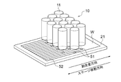
図1は、本実施形態の露光装置を示す概略構成図である。
露光装置100は、空間光変調部(空間光変調素子)で変調した光を結像光学系に通し、この光による像を感光材料(レジスト)上に結像させて露光する装置である。このような露光装置は、空間光変調素子で画像を直接形成するため、マスク(ないしはレチクル)が不要であり、DI(ダイレクト・イメージ:直描)露光装置とよばれる。
露光装置100は、露光ヘッドユニット10と、露光対象となる基板(ワーク)Wを搬送する搬送系20と、露光ヘッドユニット10及び搬送系20を設置する厚板状の設置台30とを備える。ここで、ワークWは、例えばレジストを塗布した樹脂製のプリント基板である。
露光ヘッドユニット10は、設置台30を跨ぐように設けられた門状のゲート(ガントリー)31に固定されており、ゲート31の各端部は、それぞれ設置台30の側面に固定されている。また、設置台30は、複数(例えば4本)の脚部32によって支持されている。
図1は、本実施形態の露光装置を示す概略構成図である。
露光装置100は、空間光変調部(空間光変調素子)で変調した光を結像光学系に通し、この光による像を感光材料(レジスト)上に結像させて露光する装置である。このような露光装置は、空間光変調素子で画像を直接形成するため、マスク(ないしはレチクル)が不要であり、DI(ダイレクト・イメージ:直描)露光装置とよばれる。
露光装置100は、露光ヘッドユニット10と、露光対象となる基板(ワーク)Wを搬送する搬送系20と、露光ヘッドユニット10及び搬送系20を設置する厚板状の設置台30とを備える。ここで、ワークWは、例えばレジストを塗布した樹脂製のプリント基板である。
露光ヘッドユニット10は、設置台30を跨ぐように設けられた門状のゲート(ガントリー)31に固定されており、ゲート31の各端部は、それぞれ設置台30の側面に固定されている。また、設置台30は、複数(例えば4本)の脚部32によって支持されている。
搬送系20は、真空吸着等の方法によりワークWを吸着保持する平板状のステージ21と、ステージ21の移動方向に沿って延びる2本のガイド22と、ステージ21の移動機構を一例として構成する電磁石23とを備える。ここでは、上記移動機構として、リニアモータステージを採用する。リニアモータステージは、格子状に強磁性体の凸極が設けられた平面状のプラテンの上に移動体(ステージ)をエアーにより浮上させ、移動体に磁力を印加して、移動体とプラテンの凸極との間の磁力を変化させることにより移動体(ステージ)を移動する機構である。なお、上記移動機構としては、例えばボールねじを用いた機構を採用することもできる。
ステージ21は、その長手方向がステージ移動方向に向くように配置されると共に、ガイド22によって真直度を補償した状態で往復移動可能に支持されている。
本明細書では、ステージ21の移動方向をX方向とし、X方向に垂直な水平方向をY方向、鉛直方向をZ方向とする。ワークWは方形であり、一辺の方向がX方向に向き、他方の辺がY方向を向いた姿勢でステージ21上に保持されている。なお、以下の説明では、X方向をワークWの長さ方向、Y方向をワークWの幅方向ということもある。
ステージ21の移動経路は、露光ヘッドユニット10の真下を通るように設計されており、搬送系20は、ワークWを露光ヘッドユニット10による光の照射位置に搬送し、且つその照射位置を通過させるように構成されている。この通過の過程で、露光ヘッドユニット10によって形成した像のパターンがワークWに露光される。
本明細書では、ステージ21の移動方向をX方向とし、X方向に垂直な水平方向をY方向、鉛直方向をZ方向とする。ワークWは方形であり、一辺の方向がX方向に向き、他方の辺がY方向を向いた姿勢でステージ21上に保持されている。なお、以下の説明では、X方向をワークWの長さ方向、Y方向をワークWの幅方向ということもある。
ステージ21の移動経路は、露光ヘッドユニット10の真下を通るように設計されており、搬送系20は、ワークWを露光ヘッドユニット10による光の照射位置に搬送し、且つその照射位置を通過させるように構成されている。この通過の過程で、露光ヘッドユニット10によって形成した像のパターンがワークWに露光される。
ゲート31のX方向における一方の側には上記露光ヘッドユニット10が設けられ、他方の側にはワークWの先端および後端を検知する複数(例えば2個)のセンサ40が設けられている。すなわち、露光ヘッドユニット10およびセンサ40が設けられたゲート31は、ステージ21の移動経路の上流に固定配置されている。なお、露光ヘッドユニット10およびセンサ40は、これらを制御する図示しないコントローラに接続されている。
露光ヘッドユニット10は、図2に示すように、m行n列の略マトリクス状に配列された複数(図2では14個)の露光ヘッド11を備える。各露光ヘッド11は、上述した空間光変調素子を内蔵しており、予め設定されたパターンで光を照射する。各露光ヘッド11による露光エリア51は、副走査方向を短辺とする矩形状である。したがって、ステージ21の移動に伴い、ワークWには露光ヘッド11毎に帯状の露光済みエリア52が形成される。
露光ヘッドユニット10は、図2に示すように、m行n列の略マトリクス状に配列された複数(図2では14個)の露光ヘッド11を備える。各露光ヘッド11は、上述した空間光変調素子を内蔵しており、予め設定されたパターンで光を照射する。各露光ヘッド11による露光エリア51は、副走査方向を短辺とする矩形状である。したがって、ステージ21の移動に伴い、ワークWには露光ヘッド11毎に帯状の露光済みエリア52が形成される。
空間光変調素子としては、例えば図3に示すデジタル・マイクロミラー・デバイス(DMD)12を使用する。DMD12は、メモリセル(例えば、SRAMセル)121上に、各画素(ピクセル)を構成する13μm角程度の微小ミラー(マイクロミラー)122を二次元状に配列した構成を有する。マイクロミラー122の配列数は、例えば1024個×768個である。各ピクセルにおいて、最上部には支柱に支えられた矩形のマイクロミラー122が設けられており、マイクロミラー122の表面には、例えばアルミニウム等の反射率の高い材料が蒸着されている。なお、隣接するマイクロミラー122間には、1μm以下の微小な隙間が存在する。
DMD12のSRAMセル121にデジタル信号が書き込まれると、支柱に支えられた各マイクロミラー122が、対角線を中心としてDMD12が配置された基板側に対して±α度のいずれかに傾けられる。このように、各マイクロミラー122の傾きが制御されることにより、DMD12に入射した光は各マイクロミラー122の傾き方向へ反射される。
各マイクロミラー122のオンオフ制御は、DMD12に接続された図示しないコントローラによって行われる。当該コントローラは、ワークW上に所望のパターンを形成するように、DMD12の各マイクロミラー122の角度を制御する。すなわち、DMD12の各マイクロミラー122の角度は、形成すべき画像のパターンに応じて選択的に制御される。
各マイクロミラー122のオンオフ制御は、DMD12に接続された図示しないコントローラによって行われる。当該コントローラは、ワークW上に所望のパターンを形成するように、DMD12の各マイクロミラー122の角度を制御する。すなわち、DMD12の各マイクロミラー122の角度は、形成すべき画像のパターンに応じて選択的に制御される。
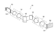
露光ヘッド11は、図4に示すように、DMD12の光入射側に、光源部13と、入射光学系14と、ミラー15とを備える。
光源部13は、例えば波長400nmのレーザ光を出射するランプや半導体レーザ(レーザダイオード)等の光源を備える。この光源部13は、上記光源の出力光を導く光ファイバを備える。ここで、光ファイバとしては、例えば石英のファイバを用いることができる。当該光ファイバの出射端部(発光点)は、露光エリア51の長辺方向と対応する方向に沿って一列に配列され、レーザ出射部131を構成する。
入射光学系14は、光源部13から出射されたレーザ光をDMD12上に入射させるための光学系である。なお、図4では、入射光学系14を概略的に示している。
ミラー15は、入射光学系14を出射したレーザ光をDMD12に向けて反射する。
入射光学系14は、図5に示すように、照明光学系141と、マイクロレンズアレイ(MLA)142と、第一の結像光学系143とを備える。
光源部13は、例えば波長400nmのレーザ光を出射するランプや半導体レーザ(レーザダイオード)等の光源を備える。この光源部13は、上記光源の出力光を導く光ファイバを備える。ここで、光ファイバとしては、例えば石英のファイバを用いることができる。当該光ファイバの出射端部(発光点)は、露光エリア51の長辺方向と対応する方向に沿って一列に配列され、レーザ出射部131を構成する。
入射光学系14は、光源部13から出射されたレーザ光をDMD12上に入射させるための光学系である。なお、図4では、入射光学系14を概略的に示している。
ミラー15は、入射光学系14を出射したレーザ光をDMD12に向けて反射する。
入射光学系14は、図5に示すように、照明光学系141と、マイクロレンズアレイ(MLA)142と、第一の結像光学系143とを備える。
照明光学系141は、インテグレータレンズやコリメートレンズ、プリズム等によって構成され、光源部13のレーザ出射部131から出射したレーザ光を平行光としてMLA142に入射する。MLA142は、微小な凸レンズ(マイクロレンズ素子)が二次元状に多数配列した光学部品である。各マイクロレンズ素子は、DMD12の各マイクロミラー122に1対1で対応している。第一の結像光学系143は、MLA142によりスポット状に集光した光を、例えば縮小してDMD12に結像する縮小結像光学系である。すなわち、DMD12とMLA142とは、一つのマイクロレンズ素子から出射した光が、第一の結像光学系143を通過して特定の一つのマイクロミラー122上に集光するように位置合わせして配置されている。
また、露光ヘッド11は、図4および図5に示すように、DMD12の光出射側に第二の結像光学系16を備える。第二の結像光学系16は、DMD12からの像を、例えば5倍に拡大してワークW上に投影する拡大結像光学系である。
露光装置100の不図示のコントローラは、形成すべき画像(露光パターン)のデジタルデータ(元データ)を記憶しており、搬送系20に制御信号を送り、ワークWが載置されたステージ21を所定速度で移動させる。また、同時にコントローラは、DMD12に制御信号を送り、ワークW上に元データに基づいた露光パターンが形成されるように所定のタイミング及びシーケンスで各マイクロミラー122の角度を制御する。この結果、レジストを塗布したワークWが露光エリア51を通過すると、ワークWに、元データによる露光パターンが形成される。
露光装置100の不図示のコントローラは、形成すべき画像(露光パターン)のデジタルデータ(元データ)を記憶しており、搬送系20に制御信号を送り、ワークWが載置されたステージ21を所定速度で移動させる。また、同時にコントローラは、DMD12に制御信号を送り、ワークW上に元データに基づいた露光パターンが形成されるように所定のタイミング及びシーケンスで各マイクロミラー122の角度を制御する。この結果、レジストを塗布したワークWが露光エリア51を通過すると、ワークWに、元データによる露光パターンが形成される。
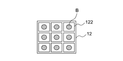
以上のように、本実施形態における露光装置100は、DMD12の前段(光入射側)にMLA142を配置し、第一の結像光学系143を介して、DMD12のマイクロミラー122上にスポット状の光を集光させる構成を有する。MLA142は、平行光とされた光源部13からの光を各マイクロレンズによって区分して集光し、第一の結像光学系143は、図6に示すように、MLA142によって集光されたスポット状の光(レーザビームB)をDMD12の各マイクロミラー122に結像する。このとき、レーザビームBは、例えば13μm角のマイクロミラー122上で直径2.4μm程度に集光される。このように、露光装置100は、DMD12のマイクロミラー122上にスポット状の光を集光させるので、光の損失を抑制し、素子効率を向上させることができる。以下、この点について詳細に説明する。
図7は、DMDの光出射側にMLAを配置した従来構成の露光ヘッド111を示す図である。この図7に示すように、露光ヘッド111は、DMD112の光入射側に、光源部113と、照明光学系114と、ミラー115とを備える。また、露光ヘッド111は、DMD112の光出射側に、第一の結像レンズ116と、MLA117と、第二の結像レンズ118とを備える。ここで、光源部113、照明光学系114及びミラー115は、図5に示す光源部13、照明光学系141及びミラー15と同様の構成を有する。また、第一の結像レンズ116及び第二の結像レンズ118は、例えば拡大投影レンズである。なお、第一の結像レンズ116は、等倍投影レンズや縮小投影レンズであってもよい。
この露光ヘッド111は、光源部113からの光を照明光学系114が平行光とし、これをDMD112に入射する。すなわち、図8に示すように、光源からの光(レーザビームB)はDMD112の全面に照射される。上述したように、隣接するマイクロミラー1122間には微小な隙間が存在するため、この隙間に入射したレーザビームBは、DMD112の基板材料に吸収されて光損失となる。また、DMD112の基板材料がレーザビームBを吸収することで素子が劣化したり、DMD112の温度が上昇して素子の劣化を促進したりするおそれもある。
これに対して、本実施形態では、露光装置100は、図6に示すように、DMD12のマイクロミラー122上にスポット状の光を集光させるため、マイクロミラー122間に形成された隙間にレーザビームBが照射されることはない。したがって、マイクロミラー122面以外への光照射による損失を抑制することができ、その分だけDMD12による光出力を向上させることができる。このように、露光装置100は、DMD12の素子効率を向上させることができる。
さらに、DMD12の基板材料がレーザビームBを吸収することを抑制することができるため、素子の劣化を抑制することができる。したがって、DMD12の長寿命化が図れる。その結果、露光装置100は、DMD12の交換頻度を少なくすることができ、スループットを向上させることができる。
また、図7に示す露光ヘッド111のように、DMD112の光出射側にMLA117を配置した構成の場合、DMD112とMLA117との位置合わせには高い精度が求められる。これは、DMD112を構成するマイクロミラーとMLA117を構成するマイクロレンズとが一対一の関係にあり、1つのマイクロミラーの反射光を対応する1つのマイクロレンズに正確に入射させる必要があるためである。1つのマイクロミラーからの光が複数のマイクロレンズに入射すると、解像性能が低下し、消光比が低下してしまう。
また、図7に示す露光ヘッド111のように、DMD112の光出射側にMLA117を配置した構成の場合、DMD112とMLA117との位置合わせには高い精度が求められる。これは、DMD112を構成するマイクロミラーとMLA117を構成するマイクロレンズとが一対一の関係にあり、1つのマイクロミラーの反射光を対応する1つのマイクロレンズに正確に入射させる必要があるためである。1つのマイクロミラーからの光が複数のマイクロレンズに入射すると、解像性能が低下し、消光比が低下してしまう。
これに対して、本実施形態では、上述したように1つのマイクロレンズを通過した光は直径2.4μm程度に集光されて13μm角のマイクロミラー122上で結像される。したがって、DMD12とMLA142との位置合わせにおける要求精度は、上記の従来構成と比較して低く、アライメント作業が容易となる。また、露光装置100は、上記の従来構成のように1つのマイクロミラーからの光が複数のマイクロレンズに入射するおそれがないため、解像性能の低下を防止し、消光比を向上させることができる。
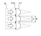
ところで、MLAは複数のマイクロレンズが配列した構成を有するが、隣接するマイクロレンズとの接合部に入射した光は迷光となり得る。そのため、これを防止するために、例えば図9に示すように、MLA117の光入射側に遮光部材117aを設け、上記接合部への光の入射を遮断することが考えられている。ここで、遮光部材117aとしては、例えばクロム系材料を含む遮光膜を用いることができる。つまり、露光ヘッド111は、遮光部材117aによって形成される開口部を通過した光だけをMLA117に入射し、露光に寄与するようにする。この場合、光学系の効率を低下させないためには、上記の接合部など、MLA117の集光性能が十分でない範囲のみを遮光し、当該開口部をできるだけ大きく設定する必要がある。
しかしながら、図7に示す露光ヘッド111のように、DMD112の各マイクロミラーからの光をMLA117の対応するマイクロレンズに入射する構成の場合、上記開口部を大きくすると、隣接する画素間でクロストークが発生するおそれがある。DMD112とMLA117との位置合わせ精度には限界があるため、当該開口部はある程度以上に大きくすることはできない。すなわち、図9に示すように、遮光部材117aによって形成される開口部を通過し、マイクロレンズを透過する光の領域である光有効領域Aは、マイクロレンズの光透過可能領域Bよりも狭くせざるを得ない。そのため、MLA117において光の損失が生じる。例えば、マイクロレンズのセルサイズが39.73μm角であり、開口部の大きさが37μm角である場合、面積比で30%以上の光が遮光部材に吸収され、これがそのまま光の損失となる。
これに対して、本実施形態の露光装置100は、MLA142によって集光したスポット状の光をDMD12のマイクロミラー上に結像するので、隣接する画素間でのクロストークの発生を抑制することができる。また、MLA142には、光源からの光が全面に入射される。すなわち、MLA142の各マイクロレンズに選択的に光が入射される構成ではない。そのため、上述した遮光部材117aに対応する遮光部材をMLA142に設ける必要がないか、若しくは、MLA142の集光性能が十分でない範囲のみを遮光し、開口部をできるだけ大きく設定した遮光部材を用いることができる。遮光部材を無くした場合、約40%の出力の向上が図れる。
以上のように、MLA117をDMD112の光出射側に配置する従来構成では、MLA117とDMD112とでそれぞれ光が蹴られることになり、大幅な光の損失となる。これに対して、本実施形態の露光装置100は、MLA142をDMD12の光入射側に配置することで、蹴られによる光の損失を防止し、光学系の効率を上げることができる。したがって、露光面における光強度を強くし、スループットを向上させることができる。
また、本実施形態における露光装置100は、光の損失を低減することができるので、露光面における光強度を図7に示す従来装置と同等とした場合、当該従来装置と比較して光源からの光強度を弱めることができる。すなわち、DMDに入射する光の強度を、従来装置よりも弱めることができる。したがって、DMD面やDMDヒンジ等への負荷を低減し、DMD部の温度上昇を緩和することができる。そのため、DMDの劣化を抑制することができる。その結果、DMDの交換頻度を低減し、メンテナンスコストを低減することができる。
また、本実施形態における露光装置100は、光の損失を低減することができるので、露光面における光強度を図7に示す従来装置と同等とした場合、当該従来装置と比較して光源からの光強度を弱めることができる。すなわち、DMDに入射する光の強度を、従来装置よりも弱めることができる。したがって、DMD面やDMDヒンジ等への負荷を低減し、DMD部の温度上昇を緩和することができる。そのため、DMDの劣化を抑制することができる。その結果、DMDの交換頻度を低減し、メンテナンスコストを低減することができる。
また、本実施形態における露光装置100は、MLA142によって集光した光をDMD12上に結像するために、第一の結像光学系143を備える。この第一の結像光学系143は縮小結像光学系であるため、MLA142によって集光した光は縮小されてDMD12上に結像される。したがって、集光スポットサイズの比較的大きなMLA142を採用することが可能であり、MLA142の製造が容易である。
さらに、本実施形態における露光装置100は、DMD12によって変調した光を露光面に結像するために、第二の結像光学系16を備える。この第二の結像光学系16は拡大結像光学系であるため、DMD12によって変調された光は拡大されて露光面上に結像される。DMD12のマイクロミラー122上において例えば直径2.4μm程度に集光された光は、DMD12によって変調された後、第二の結像光学系16によって例えば5倍に拡大され、露光面において直径12μmのスポットとなる。このとき、第二の結像光学系の拡大倍率を調整することで、露光面におけるスポットサイズを調整することができる。したがって、適切に解像度要求を満たすことができる。
さらに、本実施形態における露光装置100は、DMD12によって変調した光を露光面に結像するために、第二の結像光学系16を備える。この第二の結像光学系16は拡大結像光学系であるため、DMD12によって変調された光は拡大されて露光面上に結像される。DMD12のマイクロミラー122上において例えば直径2.4μm程度に集光された光は、DMD12によって変調された後、第二の結像光学系16によって例えば5倍に拡大され、露光面において直径12μmのスポットとなる。このとき、第二の結像光学系の拡大倍率を調整することで、露光面におけるスポットサイズを調整することができる。したがって、適切に解像度要求を満たすことができる。
(変形例)
上記実施形態においては、空間光変調素子として、反射型の空間光変調素子であるDMD12を用いる場合について説明したが、例えば液晶を用いた透過型の空間光変調素子を用いることもできる。ただし、光利用効率が高いDMDを空間光変調素子として用いることで、光源からの光を効率的に露光光として利用することができるので好ましい。
また、上記実施形態においては、第一の結像光学系として縮小結像光学系を用いる場合について説明したが、第一の結像光学系は等倍結像光学系であってもよいし、拡大結像光学系であってもよい。また、第二の結像光学系として拡大結像光学系を用いる場合について説明したが、第二の結像光学系は等倍結像光学系であってもよいし、縮小結像光学系であってもよい。
なお、上記において特定の実施形態が説明されているが、当該実施形態は単なる例示であり、本発明の範囲を限定する意図はない。本明細書に記載された装置及び方法は上記した以外の形態において具現化することができる。また、本発明の範囲から離れることなく、上記した実施形態に対して適宜、省略、置換及び変更をなすこともできる。かかる省略、置換及び変更をなした形態は、請求の範囲に記載されたもの及びこれらの均等物の範疇に含まれ、本発明の技術的範囲に属する。
上記実施形態においては、空間光変調素子として、反射型の空間光変調素子であるDMD12を用いる場合について説明したが、例えば液晶を用いた透過型の空間光変調素子を用いることもできる。ただし、光利用効率が高いDMDを空間光変調素子として用いることで、光源からの光を効率的に露光光として利用することができるので好ましい。
また、上記実施形態においては、第一の結像光学系として縮小結像光学系を用いる場合について説明したが、第一の結像光学系は等倍結像光学系であってもよいし、拡大結像光学系であってもよい。また、第二の結像光学系として拡大結像光学系を用いる場合について説明したが、第二の結像光学系は等倍結像光学系であってもよいし、縮小結像光学系であってもよい。
なお、上記において特定の実施形態が説明されているが、当該実施形態は単なる例示であり、本発明の範囲を限定する意図はない。本明細書に記載された装置及び方法は上記した以外の形態において具現化することができる。また、本発明の範囲から離れることなく、上記した実施形態に対して適宜、省略、置換及び変更をなすこともできる。かかる省略、置換及び変更をなした形態は、請求の範囲に記載されたもの及びこれらの均等物の範疇に含まれ、本発明の技術的範囲に属する。
100…露光装置、10…露光ヘッドユニット、11…露光ヘッド、12…DMD、121…SRAMセル(メモリセル)、122…マイクロミラー、13…光源、14…入射光学系、141…照明光学系、142…マイクロレンズアレイ(MLA)、143…第一の結像光学系、15…ミラー、16…第二の結像光学系、20…搬送系、21…ステージ、22…ガイド、23…電磁石、30…設置台、31…ゲート(ガントリー)、32…脚部、51…露光エリア、52…露光済みエリア、W…ワーク
Claims (6)
- 光源からの光を集光するマイクロレンズがアレイ状に配列されたマイクロレンズアレイと、
前記マイクロレンズアレイによって集光された光を変調する画素部が配列された空間光変調部と、
前記マイクロレンズアレイによって集光された光を前記空間光変調部に結像する第一の結像光学系と、
前記空間光変調部によって変調された光を感光材料上に結像する第二の結像光学系と、を備えることを特徴とする露光装置。 - 前記空間光変調部は、デジタル・マイクロミラー・デバイスであり、
前記画素部は、前記マイクロレンズと一対一に対応するマイクロミラーであることを特徴とする請求項1に記載の露光装置。 - 前記第一の結像光学系は、前記マイクロレンズアレイの各マイクロレンズによって集光されたスポット状の光を、それぞれ対応する前記マイクロミラー上に、当該マイクロミラーの大きさよりも小さいスポットサイズで結像することを特徴とする請求項2に記載の露光装置。
- 前記第二の結像光学系は、拡大結像光学系であることを特徴とする請求項1~3のいずれか1項に記載の露光装置。
- 前記第一の結像光学系は、縮小結像光学系であることを特徴とする請求項1~4のいずれか1項に記載の露光装置。
- 光源からの光を、マイクロレンズがアレイ状に配列したマイクロレンズアレイによって集光し、当該マイクロレンズアレイによって集光された光を画素部が配列された空間光変調部に結像し、当該空間光変調部によって変調された光を感光材料上に結像することを特徴とする露光方法。
Priority Applications (2)
| Application Number | Priority Date | Filing Date | Title |
|---|---|---|---|
| KR1020177029900A KR20170128561A (ko) | 2015-03-30 | 2016-02-19 | 노광 장치 및 노광 방법 |
| CN201680018422.9A CN107430353B (zh) | 2015-03-30 | 2016-02-19 | 曝光装置以及曝光方法 |
Applications Claiming Priority (2)
| Application Number | Priority Date | Filing Date | Title |
|---|---|---|---|
| JP2015-068555 | 2015-03-30 | ||
| JP2015068555A JP2016188923A (ja) | 2015-03-30 | 2015-03-30 | 露光装置及び露光方法 |
Publications (1)
| Publication Number | Publication Date |
|---|---|
| WO2016157697A1 true WO2016157697A1 (ja) | 2016-10-06 |
Family
ID=57005532
Family Applications (1)
| Application Number | Title | Priority Date | Filing Date |
|---|---|---|---|
| PCT/JP2016/000908 Ceased WO2016157697A1 (ja) | 2015-03-30 | 2016-02-19 | 露光装置及び露光方法 |
Country Status (5)
| Country | Link |
|---|---|
| JP (1) | JP2016188923A (ja) |
| KR (1) | KR20170128561A (ja) |
| CN (1) | CN107430353B (ja) |
| TW (1) | TWI649632B (ja) |
| WO (1) | WO2016157697A1 (ja) |
Families Citing this family (2)
| Publication number | Priority date | Publication date | Assignee | Title |
|---|---|---|---|---|
| JP7090002B2 (ja) * | 2018-09-27 | 2022-06-23 | 株式会社オーク製作所 | 露光装置 |
| NO20190876A1 (en) * | 2019-07-11 | 2021-01-12 | Visitech As | Real time Registration Lithography system |
Citations (9)
| Publication number | Priority date | Publication date | Assignee | Title |
|---|---|---|---|---|
| JP2004126034A (ja) * | 2002-09-30 | 2004-04-22 | Fuji Photo Film Co Ltd | 画像形成装置 |
| JP2004361939A (ja) * | 2003-05-12 | 2004-12-24 | Seiko Epson Corp | プロジェクタおよび表示装置 |
| JP2005031280A (ja) * | 2003-07-10 | 2005-02-03 | Fuji Photo Film Co Ltd | 露光装置 |
| JP2006163339A (ja) * | 2004-05-12 | 2006-06-22 | Fuji Photo Film Co Ltd | パターン形成材料、並びにパターン形成装置及びパターン形成方法 |
| WO2007040165A1 (ja) * | 2005-09-30 | 2007-04-12 | Fujifilm Corporation | 画像露光装置 |
| JP2007094095A (ja) * | 2005-09-29 | 2007-04-12 | Olympus Imaging Corp | 投影型映像表示装置 |
| WO2008090942A1 (ja) * | 2007-01-25 | 2008-07-31 | Nikon Corporation | 露光方法、露光装置、及びマイクロデバイスの製造方法 |
| JP2008197222A (ja) * | 2007-02-09 | 2008-08-28 | Fujifilm Corp | ポジ型感光性組成物及びパターン形成方法 |
| JP2013543647A (ja) * | 2010-06-11 | 2013-12-05 | オーボテック リミテッド | 光学シアリングのシステムと方法 |
Family Cites Families (8)
| Publication number | Priority date | Publication date | Assignee | Title |
|---|---|---|---|---|
| JP2002090696A (ja) * | 2000-09-20 | 2002-03-27 | Sony Corp | 光学装置及び投射型表示装置 |
| WO2003025656A1 (en) * | 2001-09-03 | 2003-03-27 | Kabushiki Kaisha Hayashi Soken | Digital control scanning method and apparatus |
| JP4057937B2 (ja) * | 2003-03-25 | 2008-03-05 | 富士フイルム株式会社 | 露光装置 |
| WO2005109098A1 (en) * | 2004-05-12 | 2005-11-17 | Fuji Photo Film Co., Ltd. | Pattern forming material, pattern forming apparatus, and pattern forming process |
| JP2005345591A (ja) * | 2004-06-01 | 2005-12-15 | Hitachi Displays Ltd | 表示装置の製造方法及びその装置 |
| KR100726737B1 (ko) * | 2005-07-04 | 2007-06-11 | 한국과학기술원 | 마이크로렌즈 어레이와 마이크로미러 어레이를 이용한 프로젝션 디스플레이 장치 |
| US7839487B2 (en) * | 2006-04-13 | 2010-11-23 | Asml Holding N.V. | Optical system for increasing illumination efficiency of a patterning device |
| US8115904B2 (en) * | 2008-05-30 | 2012-02-14 | Corning Incorporated | Illumination system for sizing focused spots of a patterning system for maskless lithography |
-
2015
- 2015-03-30 JP JP2015068555A patent/JP2016188923A/ja not_active Ceased
-
2016
- 2016-02-19 KR KR1020177029900A patent/KR20170128561A/ko not_active Ceased
- 2016-02-19 TW TW105104941A patent/TWI649632B/zh active
- 2016-02-19 CN CN201680018422.9A patent/CN107430353B/zh active Active
- 2016-02-19 WO PCT/JP2016/000908 patent/WO2016157697A1/ja not_active Ceased
Patent Citations (9)
| Publication number | Priority date | Publication date | Assignee | Title |
|---|---|---|---|---|
| JP2004126034A (ja) * | 2002-09-30 | 2004-04-22 | Fuji Photo Film Co Ltd | 画像形成装置 |
| JP2004361939A (ja) * | 2003-05-12 | 2004-12-24 | Seiko Epson Corp | プロジェクタおよび表示装置 |
| JP2005031280A (ja) * | 2003-07-10 | 2005-02-03 | Fuji Photo Film Co Ltd | 露光装置 |
| JP2006163339A (ja) * | 2004-05-12 | 2006-06-22 | Fuji Photo Film Co Ltd | パターン形成材料、並びにパターン形成装置及びパターン形成方法 |
| JP2007094095A (ja) * | 2005-09-29 | 2007-04-12 | Olympus Imaging Corp | 投影型映像表示装置 |
| WO2007040165A1 (ja) * | 2005-09-30 | 2007-04-12 | Fujifilm Corporation | 画像露光装置 |
| WO2008090942A1 (ja) * | 2007-01-25 | 2008-07-31 | Nikon Corporation | 露光方法、露光装置、及びマイクロデバイスの製造方法 |
| JP2008197222A (ja) * | 2007-02-09 | 2008-08-28 | Fujifilm Corp | ポジ型感光性組成物及びパターン形成方法 |
| JP2013543647A (ja) * | 2010-06-11 | 2013-12-05 | オーボテック リミテッド | 光学シアリングのシステムと方法 |
Also Published As
| Publication number | Publication date |
|---|---|
| JP2016188923A (ja) | 2016-11-04 |
| TWI649632B (zh) | 2019-02-01 |
| CN107430353A (zh) | 2017-12-01 |
| CN107430353B (zh) | 2020-04-28 |
| KR20170128561A (ko) | 2017-11-22 |
| TW201636738A (zh) | 2016-10-16 |
Similar Documents
| Publication | Publication Date | Title |
|---|---|---|
| JP6652618B2 (ja) | 照度割合変更方法及び露光方法 | |
| JP6480680B2 (ja) | 照度割合変更方法及び露光方法 | |
| US9791784B2 (en) | Assembly for a projection exposure apparatus for EUV projection lithography | |
| KR100742251B1 (ko) | 화상노광방법 및 장치 | |
| TW202505314A (zh) | 空間光調變單元及曝光裝置 | |
| CN104977811B (zh) | 曝光装置及其固定方法 | |
| US7339602B2 (en) | Image-drawing device and image-drawing method | |
| JP2019015974A (ja) | 露光装置及び露光方法 | |
| CN107430353B (zh) | 曝光装置以及曝光方法 | |
| JP4979462B2 (ja) | 画像露光装置 | |
| JP7090002B2 (ja) | 露光装置 | |
| JP4679249B2 (ja) | パターン描画装置 | |
| CN1842746A (zh) | 用于形成光学图像的控制电路和方法 | |
| WO2013182367A1 (en) | Lithography apparatus and device manufacturing method | |
| JP4511502B2 (ja) | 基板露光装置 | |
| JP2004191660A (ja) | 露光装置 | |
| JP2005202226A (ja) | 感光材料の感度検出方法および装置並びに露光補正方法 | |
| US20240126178A1 (en) | Exposure apparatus, control method, and device manufacturing method | |
| US20240345486A1 (en) | Exposure device | |
| JP2006133431A (ja) | 露光方法および装置 | |
| JP5831516B2 (ja) | 画像形成装置 | |
| KR20120055782A (ko) | 마스크리스 노광장치의 노광헤드 | |
| CN118689041A (zh) | 曝光装置 | |
| KR101390512B1 (ko) | 개선된 패턴 형성용 노광 광원, 노광 장치, 노광 시스템, 및 노광 방법 | |
| JP2005202227A (ja) | 感光材料の感度検出方法および装置並びに露光補正方法 |
Legal Events
| Date | Code | Title | Description |
|---|---|---|---|
| 121 | Ep: the epo has been informed by wipo that ep was designated in this application |
Ref document number: 16771592 Country of ref document: EP Kind code of ref document: A1 |
|
| NENP | Non-entry into the national phase |
Ref country code: DE |
|
| ENP | Entry into the national phase |
Ref document number: 20177029900 Country of ref document: KR Kind code of ref document: A |
|
| 122 | Ep: pct application non-entry in european phase |
Ref document number: 16771592 Country of ref document: EP Kind code of ref document: A1 |