WO2016152647A1 - 回路構成体 - Google Patents
回路構成体 Download PDFInfo
- Publication number
- WO2016152647A1 WO2016152647A1 PCT/JP2016/058118 JP2016058118W WO2016152647A1 WO 2016152647 A1 WO2016152647 A1 WO 2016152647A1 JP 2016058118 W JP2016058118 W JP 2016058118W WO 2016152647 A1 WO2016152647 A1 WO 2016152647A1
- Authority
- WO
- WIPO (PCT)
- Prior art keywords
- circuit board
- metal chip
- bus bar
- circuit structure
- electronic component
- Prior art date
- Legal status (The legal status is an assumption and is not a legal conclusion. Google has not performed a legal analysis and makes no representation as to the accuracy of the status listed.)
- Ceased
Links
Images


Classifications
-
- H—ELECTRICITY
- H05—ELECTRIC TECHNIQUES NOT OTHERWISE PROVIDED FOR
- H05K—PRINTED CIRCUITS; CASINGS OR CONSTRUCTIONAL DETAILS OF ELECTRIC APPARATUS; MANUFACTURE OF ASSEMBLAGES OF ELECTRICAL COMPONENTS
- H05K1/00—Printed circuits
- H05K1/02—Details
- H05K1/0271—Arrangements for reducing stress or warp in rigid printed circuit boards, e.g. caused by loads, vibrations or differences in thermal expansion
-
- H—ELECTRICITY
- H05—ELECTRIC TECHNIQUES NOT OTHERWISE PROVIDED FOR
- H05K—PRINTED CIRCUITS; CASINGS OR CONSTRUCTIONAL DETAILS OF ELECTRIC APPARATUS; MANUFACTURE OF ASSEMBLAGES OF ELECTRICAL COMPONENTS
- H05K1/00—Printed circuits
- H05K1/02—Details
- H05K1/0201—Thermal arrangements, e.g. for cooling, heating or preventing overheating
- H05K1/0203—Cooling of mounted components
- H05K1/0204—Cooling of mounted components using means for thermal conduction connection in the thickness direction of the substrate
-
- H—ELECTRICITY
- H05—ELECTRIC TECHNIQUES NOT OTHERWISE PROVIDED FOR
- H05K—PRINTED CIRCUITS; CASINGS OR CONSTRUCTIONAL DETAILS OF ELECTRIC APPARATUS; MANUFACTURE OF ASSEMBLAGES OF ELECTRICAL COMPONENTS
- H05K1/00—Printed circuits
- H05K1/18—Printed circuits structurally associated with non-printed electric components
- H05K1/181—Printed circuits structurally associated with non-printed electric components associated with surface mounted components
-
- H—ELECTRICITY
- H05—ELECTRIC TECHNIQUES NOT OTHERWISE PROVIDED FOR
- H05K—PRINTED CIRCUITS; CASINGS OR CONSTRUCTIONAL DETAILS OF ELECTRIC APPARATUS; MANUFACTURE OF ASSEMBLAGES OF ELECTRICAL COMPONENTS
- H05K3/00—Apparatus or processes for manufacturing printed circuits
- H05K3/30—Assembling printed circuits with electric components, e.g. with resistors
- H05K3/32—Assembling printed circuits with electric components, e.g. with resistors electrically connecting electric components or wires to printed circuits
- H05K3/34—Assembling printed circuits with electric components, e.g. with resistors electrically connecting electric components or wires to printed circuits by soldering
- H05K3/341—Surface mounted components
-
- H—ELECTRICITY
- H05—ELECTRIC TECHNIQUES NOT OTHERWISE PROVIDED FOR
- H05K—PRINTED CIRCUITS; CASINGS OR CONSTRUCTIONAL DETAILS OF ELECTRIC APPARATUS; MANUFACTURE OF ASSEMBLAGES OF ELECTRICAL COMPONENTS
- H05K1/00—Printed circuits
- H05K1/02—Details
- H05K1/0213—Electrical arrangements not otherwise provided for
- H05K1/0263—High current adaptations, e.g. printed high current conductors or using auxiliary non-printed means; Fine and coarse circuit patterns on one circuit board
- H05K1/0265—High current adaptations, e.g. printed high current conductors or using auxiliary non-printed means; Fine and coarse circuit patterns on one circuit board characterized by the lay-out of or details of the printed conductors, e.g. reinforced conductors, redundant conductors, conductors having different cross-sections
-
- H—ELECTRICITY
- H05—ELECTRIC TECHNIQUES NOT OTHERWISE PROVIDED FOR
- H05K—PRINTED CIRCUITS; CASINGS OR CONSTRUCTIONAL DETAILS OF ELECTRIC APPARATUS; MANUFACTURE OF ASSEMBLAGES OF ELECTRICAL COMPONENTS
- H05K2201/00—Indexing scheme relating to printed circuits covered by H05K1/00
- H05K2201/06—Thermal details
- H05K2201/068—Thermal details wherein the coefficient of thermal expansion is important
-
- H—ELECTRICITY
- H05—ELECTRIC TECHNIQUES NOT OTHERWISE PROVIDED FOR
- H05K—PRINTED CIRCUITS; CASINGS OR CONSTRUCTIONAL DETAILS OF ELECTRIC APPARATUS; MANUFACTURE OF ASSEMBLAGES OF ELECTRICAL COMPONENTS
- H05K2201/00—Indexing scheme relating to printed circuits covered by H05K1/00
- H05K2201/10—Details of components or other objects attached to or integrated in a printed circuit board
- H05K2201/10227—Other objects, e.g. metallic pieces
-
- H—ELECTRICITY
- H05—ELECTRIC TECHNIQUES NOT OTHERWISE PROVIDED FOR
- H05K—PRINTED CIRCUITS; CASINGS OR CONSTRUCTIONAL DETAILS OF ELECTRIC APPARATUS; MANUFACTURE OF ASSEMBLAGES OF ELECTRICAL COMPONENTS
- H05K2201/00—Indexing scheme relating to printed circuits covered by H05K1/00
- H05K2201/10—Details of components or other objects attached to or integrated in a printed circuit board
- H05K2201/10227—Other objects, e.g. metallic pieces
- H05K2201/10272—Busbars, i.e. thick metal bars mounted on the printed circuit board [PCB] as high-current conductors
-
- H—ELECTRICITY
- H05—ELECTRIC TECHNIQUES NOT OTHERWISE PROVIDED FOR
- H05K—PRINTED CIRCUITS; CASINGS OR CONSTRUCTIONAL DETAILS OF ELECTRIC APPARATUS; MANUFACTURE OF ASSEMBLAGES OF ELECTRICAL COMPONENTS
- H05K2201/00—Indexing scheme relating to printed circuits covered by H05K1/00
- H05K2201/10—Details of components or other objects attached to or integrated in a printed circuit board
- H05K2201/10227—Other objects, e.g. metallic pieces
- H05K2201/10416—Metallic blocks or heatsinks completely inserted in a PCB
-
- Y—GENERAL TAGGING OF NEW TECHNOLOGICAL DEVELOPMENTS; GENERAL TAGGING OF CROSS-SECTIONAL TECHNOLOGIES SPANNING OVER SEVERAL SECTIONS OF THE IPC; TECHNICAL SUBJECTS COVERED BY FORMER USPC CROSS-REFERENCE ART COLLECTIONS [XRACs] AND DIGESTS
- Y02—TECHNOLOGIES OR APPLICATIONS FOR MITIGATION OR ADAPTATION AGAINST CLIMATE CHANGE
- Y02P—CLIMATE CHANGE MITIGATION TECHNOLOGIES IN THE PRODUCTION OR PROCESSING OF GOODS
- Y02P70/00—Climate change mitigation technologies in the production process for final industrial or consumer products
- Y02P70/50—Manufacturing or production processes characterised by the final manufactured product
Definitions
- the present invention relates to a circuit structure.
- a circuit structure constituting a power circuit such as an inverter or a converter is incorporated in, for example, an electrical junction box for distributing power from an in-vehicle power source to various electrical components.
- the circuit structure includes a circuit board and a plurality of bus bars bonded to the circuit board.
- the electronic components which comprise a power circuit are mounted in the circuit structure.
- the circuit structure described in Patent Document 1 includes a circuit board in which an opening is formed, and a bus bar in which a connection protrusion protruding into the opening is formed, and the connection protrusion and the electronic component The terminals are soldered.
- This circuit structure can easily confirm the state of soldering visually by comparison with a case where the bus bar does not have a connection protrusion. Therefore, the connection reliability of the electronic component can be improved.
- the conventional circuit structure still has room for improvement in the following points.
- the connection protrusion is provided by a method such as pressing or cutting
- the thickness of the circuit board is restricted. Therefore, when the connection protrusion is provided by a method such as press working, it is difficult to improve the rigidity of the circuit structure by increasing the thickness of the circuit board.
- connection protrusion when the connection protrusion is provided by driving the conductor into the bus bar, the joint area between the conductor and the bus bar tends to be relatively small. Therefore, the electrical resistance and thermal resistance between the conductor and the bus bar tend to increase. Therefore, when the connection protrusion is provided by driving a conductor into the bus bar, there is a possibility that problems such as insufficient cooling of the electronic component or an increase in electrical resistance between the electronic component and the bus bar may occur. .
- the conventional circuit rigid body still has room for improvement in order to improve the cooling performance of the electronic component and reduce the electrical resistance between the electronic component and the bus bar while further improving the rigidity. There is.
- the present invention has been made in view of such a background, and provides a circuit structure that has high rigidity, high cooling performance of electronic components, and can reduce electrical resistance between the electronic components and the bus bar. It is something to try.
- One aspect of the present invention is a circuit board having an opening penetrating in the thickness direction; A plurality of bus bars made of a conductor and superimposed on the circuit board; An adhesive that is interposed between the circuit board and the plurality of bus bars to bond them; A metal chip placed in the opening and placed on the bus bar; An electronic component soldered to both the circuit board and the metal chip;
- the metal chip has a top surface that exists on substantially the same plane as the opening end surface of the opening, and a bottom surface in which substantially the entire surface is joined to the bus bar.
- the electronic component is in a circuit structure that is soldered to the top surface of the metal chip.
- the circuit structure has a metal chip placed in the opening and placed on the bus bar.
- the metal chip has a top surface that exists on substantially the same plane as the opening end surface of the opening, and a bottom surface that is substantially entirely joined to the bus bar.
- the circuit configuration body is configured by joining the bus bar and the metal chip, which are separately prepared. Therefore, by using the metal chip corresponding to the thickness of the circuit board, the position of the top surface can be easily aligned with the opening end surface of the opening. Therefore, in the circuit configuration body, the thickness of the circuit board can be easily increased, and as a result, the rigidity can be improved.
- the bonding area between the metal chip and the bus bar can be easily increased.
- the circuit component can efficiently cool the electronic component and can reduce the electrical resistance between the electronic component and the bus bar.
- the circuit configuration body has high rigidity, high cooling performance of the electronic component, and can reduce the electrical resistance between the electronic component and the bus bar.
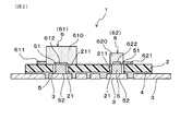
- FIG. 3 is a perspective view illustrating a main part of a circuit configuration body according to the first embodiment.
- FIG. 3 is a partial cross-sectional view showing the main part of the circuit configuration body in Example 1.
- the partial cross section figure which shows the principal part of the circuit structure body in which the metal chip and the bus bar in Example 2 were soldered.
- a metal having excellent electrical conductivity and thermal conductivity can be used as the material of the metal chip.
- copper, copper alloy, aluminum, aluminum alloy, iron, iron alloy, zinc, tungsten, gold, silver, tin, nickel, etc. can be adopted as the material of the metal chip.
- the metal tip is preferably made of a metal having a linear expansion coefficient of 15 to 45 ppm / ° C.
- a circuit board used for the circuit structure a glass epoxy board based on FR-4 (Flame Retardant type 4) or the like is frequently used. These circuit boards have a linear expansion coefficient in the thickness direction of about 20 to 50 ppm / ° C. in the operating temperature range of the circuit component.
- the value of the linear expansion coefficient in the thickness direction of the circuit board can be brought close to the linear expansion coefficient of the metal chip.
- the thermal stress applied to the solder for joining the electronic component and the metal chip and the solder for joining the electronic component and the circuit board can be reduced, and as a result, the connection reliability of the electronic component can be further improved.
- the linear expansion coefficient of the metal chip When the linear expansion coefficient of the metal chip is out of the specific range, the thermal stress applied to the solder tends to increase. Further, since the thermal stress applied to the solder becomes large, cracks and the like are likely to occur in the solder, which may result in poor connection of electronic components. In order to suppress the occurrence of such a problem, it is preferable to use a metal tip having a linear expansion coefficient in the specific range. From the same viewpoint, the linear expansion coefficient of the metal tip is more preferably in the range of 15 to 25 ppm / ° C.
- the circuit structure 1 includes a circuit board 2, a plurality of bus bars 3, an adhesive 4, a metal chip 5, and an electronic component 6.
- the circuit board 2 has an opening 21 penetrating in the thickness direction.
- the plurality of bus bars 3 are made of a conductor and overlapped with the circuit board 2.
- the adhesive 4 is interposed between the circuit board 2 and the plurality of bus bars 3, and both are bonded by the adhesive 4.
- the metal chip 5 is placed in the opening 21 and placed on the bus bar 3.
- the electronic component 6 is soldered (not shown) to both the circuit board 2 and the metal chip 5.
- the metal chip 5 has a top surface 51 that exists on substantially the same plane as the opening end surface 211 of the opening portion 21, and a bottom surface 52 that is joined to the bus bar 3. ing.
- the electronic component 6 is soldered (not shown) to the top surface 51 of the metal chip 5.
- the circuit structure 1 of this example will be described in detail.
- the bus bar 3 is made of copper or a copper alloy.
- the bus bar 3 of this example can be produced by appropriately performing punching or bending on a copper plate or a copper alloy plate, for example.
- the circuit board 2 has a plurality of openings 21 penetrating in the thickness direction.
- the opening 21 is arranged on the bus bar 3 as shown in FIG. 2, and is configured so that the metal chip 5 can be placed in the opening 21.
- the circuit board 2 in this example is a glass epoxy board made of FR-4 material.
- the linear expansion coefficient in the thickness direction of the FR-4 material near room temperature is typically about 30 ppm / ° C.
- a conventionally known adhesive 4 such as a thermosetting epoxy resin can be used.
- the metal chip 5 disposed in the opening 21 of the circuit board 2 has substantially the same thickness as the circuit board 2. Further, the metal chip 5 faces the side peripheral surface of the circuit board 2 through a gap in a state where the metal chip 5 is disposed in the opening 21.
- the metal tip 5 of this example is made of brass.
- the linear expansion coefficient of brass is typically about 21 ppm / ° C.
- the metal tip 5 is directly joined to the bus bar 3 by ultrasonic welding. That is, after the metal chip 5 of this example is placed on the bus bar 3, it is joined to the bus bar 3 by pressing the top surface 51 while applying ultrasonic waves.
- Examples of the electronic component 6 to be soldered to the circuit board 2 and the metal chip 5 include switching elements such as a mechanical relay switch 61 and a semiconductor switching element 62.
- the mechanical relay switch 61 has a control terminal 611 for inputting a switching signal for controlling the switching of the contacts, and a main terminal 612 for flowing a current to the bus bar 3 corresponding to the switching state of the contacts.
- the main body 610 of the mechanical relay switch 61 is placed on the circuit board 2.
- the control terminal 611 is soldered to the land 22 of the circuit board 2.
- the main terminal 612 is soldered to the top surface 51 of the metal chip 5 and is electrically connected to the bus bar 3 via the metal chip 5.
- the semiconductor switching element 62 for example, a MOSFET (Metal-Oxide-Semiconductor Field-Effect Transistor) or the like can be used. As shown in FIG. 2, the main body 620 of the semiconductor switching element 62 is placed on the metal chip 5. The gate terminal 621 of the semiconductor switching element 62 is soldered to the land 22 of the circuit board 2. The source terminal 622 and the drain terminal (not shown) of the semiconductor switching element 62 are soldered to the top surface 51 of the metal chip 5.
- MOSFET Metal-Oxide-Semiconductor Field-Effect Transistor
- circuit board 2 of this example examples include resistors, inductors, capacitors, and diodes.
- a control circuit that is a part of the power circuit is configured by these electronic components. The driving of the mechanical relay switch 61 and the semiconductor switching element 62 is controlled by a switching signal or the like output from the control circuit.
- the metal chip 5 and the bus bar 3 are joined directly without a junction material such as solder. Therefore, the metal chip 5 and the bus bar 3 can be firmly joined. As a result, the state where the metal chip 5 and the bus bar 3 are joined can be maintained for a long period of time, and the connection reliability can be improved.
- the circuit structure 1 of this example since a metal bond is formed between the metal chip 5 and the bus bar 3, the thermal resistance and electrical resistance between the two can be further reduced. Therefore, the circuit structure 1 has a high cooling performance for the electronic component 6 and can reduce the electrical resistance between the electronic component 6 and the bus bar 3.
- Example 2 This example is an example of the circuit structure 1b in which the metal chip 5 and the bus bar 3 are bonded using a conductive bonding material. As shown in FIG. 3, in the circuit configuration body 1 b of this example, a bonding material 7 is interposed between the metal chip 5 and the bus bar 3, and the metal chip 5 is bonded to the bus bar 3 via the bonding material 7. ing.
- the bonding material 7 for example, a conductive material such as solder or metal nano paste can be used.
- solder is used as the bonding material 7, the metal chip 5 and the bus bar 3 can be bonded by various methods such as a reflow soldering method, a hot press method, and an ultrasonic soldering method.
- Others are the same as in the first embodiment. 3 that are the same as those used in the first embodiment represent the same components as those in the first embodiment unless otherwise specified.
Landscapes
- Engineering & Computer Science (AREA)
- Microelectronics & Electronic Packaging (AREA)
- Manufacturing & Machinery (AREA)
- Connection Or Junction Boxes (AREA)
- Structures For Mounting Electric Components On Printed Circuit Boards (AREA)
Abstract
高い剛性を有し、電子部品の冷却性能が高く、電子部品とバスバーとの間の電気抵抗を小さくすることができる回路構成体(1)を提供する。回路構成体(1)は、回路基板(2)、複数のバスバー(3)、接着材(4)、金属チップ(5)及び電子部品(6)を有している。回路基板(2)は厚み方向に貫通した開口部(21)を有している。複数のバスバー(3)は回路基板(2)に重ね合わされている。接着材(4)は回路基板(2)と複数のバスバー(3)との間に介在しており、両者を接着している。金属チップ(5)は開口部(21)内に配置されると共にバスバー(3)上に載置されている。金属チップ(5)は、開口部(21)の開口端面(211)と略同一の平面上に存在している頂面(51)と、略全面がバスバー(3)に接合された底面(52)とを有している。電子部品(6)は回路基板(2)及び金属チップ(5)の頂面(51)にはんだ付けされている。
Description
本発明は、回路構成体に関する。
インバータやコンバータ等の電力回路を構成する回路構成体は、例えば、車載電源から各種電装品へ電力を分配するための電気接続箱等に組み込まれている。回路構成体は、回路基板と、回路基板に接着された複数のバスバーとを有している。また、回路構成体には電力回路を構成する電子部品が実装されている。
例えば、特許文献1に記載された回路構成体は、開口部が形成された回路基板と、開口部内に突出する接続突部が形成されたバスバーとを有しており、接続突部と電子部品の端子とがはんだ付けされている。この回路構成体は、バスバーに接続突部を有しない場合に比べてはんだ付けの状態を目視により容易に確認することができる。それ故、電子部品の接続信頼性を改善することができる。
また、バスバーに接続突部を設けることにより、電子部品の接続信頼性を損なうことなく、回路基板の厚みを容易に厚くすることができる。その結果、回路構成体の剛性を従来よりも大きくすることができ、ひいては回路構成体の反りや歪みを低減する効果も期待することができる。
しかし、従来の回路構成体は、以下の点について未だ改善の余地がある。例えば特許文献1に記載されているように、プレス加工や切り起こし等の方法により接続突部を設ける場合には、接続突部の高さを過度に高くしようとするとバスバーに割れが生じるおそれがある。それ故、この場合には、接続突部を高くすることには限界がある。そして、バスバーの割れを抑制する観点から接続突部の高さが制限される結果、回路基板の厚みが制限される。従って、プレス加工等の方法により接続突部を設ける場合には、回路基板を厚くすることにより回路構成体の剛性を向上させることが難しい。
また、バスバーに導体を打ち込むことにより接続突部を設ける場合には、導体とバスバーとの接合面積が比較的小さくなり易い。そのため、導体とバスバーとの間の電気抵抗及び熱抵抗が大きくなり易い。従って、バスバーに導体を打ち込むことにより接続突部を設ける場合には、電子部品の冷却が不十分となる、あるいは電子部品とバスバーとの間の電気抵抗が大きくなるなどの問題が生じるおそれがある。
以上のように、従来の回路剛性体は、剛性をより向上させた上で、電子部品の冷却性能の向上及び電子部品とバスバーとの間の電気抵抗の低減を図るためには未だ改善の余地がある。
本発明は、かかる背景に鑑みてなされたものであり、高い剛性を有し、電子部品の冷却性能が高く、電子部品とバスバーとの間の電気抵抗を小さくすることができる回路構成体を提供しようとするものである。
本発明の一態様は、厚み方向に貫通した開口部を有する回路基板と、
導体よりなり、上記回路基板に重ね合わされた複数のバスバーと、
上記回路基板と上記複数のバスバーとの間に介在して両者を接着する接着材と、
上記開口部内に配置されると共に上記バスバー上に載置された金属チップと、
上記回路基板及び上記金属チップの両者にはんだ付けされた電子部品とを有し、
該金属チップは、上記開口部の開口端面と略同一の平面上に存在している頂面と、略全面が上記バスバーに接合された底面とを有しており、
上記電子部品は上記金属チップの上記頂面にはんだ付けされている、回路構成体にある。
導体よりなり、上記回路基板に重ね合わされた複数のバスバーと、
上記回路基板と上記複数のバスバーとの間に介在して両者を接着する接着材と、
上記開口部内に配置されると共に上記バスバー上に載置された金属チップと、
上記回路基板及び上記金属チップの両者にはんだ付けされた電子部品とを有し、
該金属チップは、上記開口部の開口端面と略同一の平面上に存在している頂面と、略全面が上記バスバーに接合された底面とを有しており、
上記電子部品は上記金属チップの上記頂面にはんだ付けされている、回路構成体にある。
上記回路構成体は、上記開口部内に配置されると共に上記バスバー上に載置された金属チップを有している。また、該金属チップは、上記開口部の開口端面と略同一の平面上に存在している頂面と、略全面が上記バスバーに接合された底面とを有している。このように、上記回路構成体は、別々に準備された上記バスバーと上記金属チップとを接合して構成されている。そのため、上記回路基板の厚みに対応した上記金属チップを用いることにより、上記頂面の位置を上記開口部の開口端面に容易に揃えることができる。それ故、上記回路構成体は、上記回路基板の厚みを容易に厚くすることができ、ひいては剛性を向上させることができる。
また、上記回路構成体は、上記金属チップの上記底面における略全面が上記バスバーに接合されているため、上記金属チップと上記バスバーとの接合面積を容易に広くすることができる。その結果、上記回路構成体は、上記電子部品を効率よく冷却することができると共に、上記電子部品と上記バスバーとの間の電気抵抗を小さくすることができる。
以上のように、上記回路構成体は、高い剛性を有し、電子部品の冷却性能が高く、電子部品とバスバーとの間の電気抵抗を小さくすることができる。
上記回路構成体において、上記金属チップの材質としては、電気伝導性及び熱伝導性に優れた金属を採用することができる。具体的には、銅、銅合金、アルミニウム、アルミニウム合金、鉄、鉄合金、亜鉛、タングステン、金、銀、スズ、ニッケル等を金属チップの材質として採用することができる。
上記金属チップは、線膨張係数が15~45ppm/℃である金属より構成されていることが好ましい。回路構成体に用いられる回路基板としては、FR-4(Flame Retardant type 4)等を基材とするガラスエポキシ基板が多用されている。これらの回路基板は、回路構成体の使用温度範囲において、20~50ppm/℃程度の厚み方向の線膨張係数を有している。
それ故、上記特定の範囲の線膨張係数を有する金属チップを用いることにより、回路基板の厚み方向における線膨張係数の値を金属チップの線膨張係数に近づけることができる。その結果、電子部品と金属チップとを接合するはんだ及び電子部品と回路基板とを接合するはんだに加わる熱応力を低減することができ、ひいては電子部品の接続信頼性をより向上させることができる。
金属チップの線膨張係数が上記特定の範囲から外れる場合には、上記のはんだに加わる熱応力が大きくなり易い。そして、はんだに加わる熱応力が大きくなることにより、はんだにクラック等が発生しやすくなり、ひいては電子部品の接続不良を招くおそれがある。かかる問題の発生を抑制するため、上記特定の範囲の線膨張係数を有する金属チップを用いることが好ましい。同じ観点から、金属チップの線膨張係数は、15~25ppm/℃の範囲であることがより好ましい。
(実施例1)
上記回路構成体の実施例について、図を用いて説明する。図1及び図2に示すように、回路構成体1は、回路基板2と、複数のバスバー3と、接着材4と、金属チップ5と、電子部品6とを有している。図2に示すように、回路基板2は厚み方向に貫通した開口部21を有している。複数のバスバー3は導体より構成されており、回路基板2に重ね合わされている。接着材4は回路基板2と複数のバスバー3との間に介在しており、接着材4により両者が接着されている。金属チップ5は開口部21内に配置されると共にバスバー3上に載置されている。電子部品6は回路基板2及び金属チップ5の両者にはんだ付け(図示略)されている。
上記回路構成体の実施例について、図を用いて説明する。図1及び図2に示すように、回路構成体1は、回路基板2と、複数のバスバー3と、接着材4と、金属チップ5と、電子部品6とを有している。図2に示すように、回路基板2は厚み方向に貫通した開口部21を有している。複数のバスバー3は導体より構成されており、回路基板2に重ね合わされている。接着材4は回路基板2と複数のバスバー3との間に介在しており、接着材4により両者が接着されている。金属チップ5は開口部21内に配置されると共にバスバー3上に載置されている。電子部品6は回路基板2及び金属チップ5の両者にはんだ付け(図示略)されている。
図2に示すように、金属チップ5は、開口部21の開口端面211と略同一の平面上に存在している頂面51と、略全面がバスバー3に接合された底面52とを有している。そして、電子部品6は金属チップ5の頂面51にはんだ付け(図示略)されている。以下、本例の回路構成体1について詳説する。
バスバー3は、銅または銅合金より構成されている。本例のバスバー3は、例えば、銅板又は銅合金板に打ち抜き加工や曲げ加工等を適宜行うことにより作製することができる。
回路基板2は、厚み方向に貫通した開口部21を複数有している。開口部21は、図2に示すようにバスバー3上に配置されており、開口部21内に金属チップ5を載置できるように構成されている。なお、本例の回路基板2は、FR-4材からなるガラスエポキシ基板である。室温付近におけるFR-4材の厚み方向の線膨張係数は、典型的には30ppm/℃程度である。
バスバー3と回路基板2とを接着する接着材4には、熱硬化性エポキシ樹脂等の従来公知の接着材4を用いることができる。
回路基板2の開口部21内に配置された金属チップ5は、回路基板2と略同一の厚みを有している。また、金属チップ5は、開口部21内に配置された状態において、回路基板2の側周面と隙間を介して対面している。なお、本例の金属チップ5は、黄銅から構成されている。黄銅の線膨張係数は、典型的には21ppm/℃程度である。
本例において、金属チップ5は超音波溶接によりバスバー3と直接接合されている。即ち、本例の金属チップ5は、バスバー3上に載置された後、超音波を印加しつつ頂面51を押圧することによりバスバー3に接合されている。
回路基板2及び金属チップ5にはんだ付けされる電子部品6としては、例えば、機械式リレースイッチ61や半導体スイッチング素子62等のスイッチング素子が挙げられる。機械式リレースイッチ61は、接点の切替を制御する切替信号を入力する制御端子611と、接点の切替状態に対応してバスバー3に電流を流す主端子612とを有している。図1及び図2に示すように、機械式リレースイッチ61の本体部610は回路基板2上に載置されている。制御端子611は回路基板2のランド22にはんだ付けされている。また、主端子612は金属チップ5の頂面51にはんだ付けされており、金属チップ5を介してバスバー3に電気的に接続されている。
半導体スイッチング素子62としては、例えばMOSFET(Metal-Oxide-Semiconductor Field-Effect Transistor)等を用いることができる。図2に示すように、半導体スイッチング素子62の本体部620は金属チップ5上に載置されている。半導体スイッチング素子62のゲート端子621は回路基板2のランド22にはんだ付けされている。また、半導体スイッチング素子62のソース端子622及びドレイン端子(図示略)は金属チップ5の頂面51にはんだ付けされている。
なお、図には示さないが、本例の回路基板2上には、上述したスイッチング素子の他にも電子部品が実装されている。回路基板2上に実装される電子部品としては、例えば、抵抗、インダクタ、キャパシタ及びダイオード等が挙げられる。回路基板2上には、これらの電子部品により電力回路の一部である制御回路が構成されている。機械式リレースイッチ61及び半導体スイッチング素子62の駆動は、制御回路から出力された切替信号等により制御される。
本例の回路構成体1においては、金属チップ5とバスバー3とがはんだ等の接合材を介さずに直接接合されている。そのため、金属チップ5とバスバー3とを強固に接合することができる。その結果、金属チップ5とバスバー3とが接合された状態を長期間に亘って維持することができ、接続信頼性を向上させることができる。
また、本例の回路構成体1においては、金属チップ5とバスバー3との間に金属結合が形成されているため、両者の間の熱抵抗及び電気抵抗をより低減することができる。それ故、回路構成体1は、電子部品6の冷却性能が高く、かつ、電子部品6とバスバー3との間の電気抵抗を低減することができる。
(実施例2)
本例は、導電性を有する接合材を用いて金属チップ5とバスバー3とを接合した回路構成体1bの例である。図3に示すように、本例の回路構成体1bは、金属チップ5とバスバー3との間に接合材7が介在しており、金属チップ5が接合材7を介してバスバー3に接合されている。
本例は、導電性を有する接合材を用いて金属チップ5とバスバー3とを接合した回路構成体1bの例である。図3に示すように、本例の回路構成体1bは、金属チップ5とバスバー3との間に接合材7が介在しており、金属チップ5が接合材7を介してバスバー3に接合されている。
接合材7としては、例えば、はんだや金属ナノペースト等の導電性を有する材料を用いることができる。また、接合材7としてはんだを用いる場合には、リフローはんだ付け法、熱プレス法及び超音波はんだ付け法等の種々の方法により金属チップ5とバスバー3とを接合することができる。その他は実施例1と同様である。なお、図3において用いた符号のうち、実施例1において用いた符号と同一のものは、特に説明の無い限り実施例1と同様の構成要素等を表す。
本例のように、金属チップ5とバスバー3との接合に接合材7を用いる場合には、両者の接合を容易に行うことができる。その結果、回路構成体1bの生産性を容易に向上させることができる。
Claims (5)
- 厚み方向に貫通した開口部を有する回路基板と、
導体よりなり、上記回路基板に重ね合わされた複数のバスバーと、
上記回路基板と上記複数のバスバーとの間に介在して両者を接着する接着材と、
上記開口部内に配置されると共に上記バスバー上に載置された金属チップと、
上記回路基板及び上記金属チップの両者にはんだ付けされた電子部品とを有し、
該金属チップは、上記開口部の開口端面と略同一の平面上に存在している頂面と、略全面が上記バスバーに接合された底面とを有しており、
上記電子部品は上記金属チップの上記頂面にはんだ付けされている、回路構成体。 - 上記金属チップは、線膨張係数が15~45ppm/℃である金属より構成されている、請求項1に記載の回路構成体。
- 上記金属チップは、上記バスバーに直接接合されている、請求項1または2に記載の回路構成体。
- 上記回路構成体は、上記金属チップと上記バスバーとを接合する接合材を有しており、該接合材は導電性を有している、請求項1または2に記載の回路構成体。
- 上記回路基板の厚みが1.2mm以上である、請求項1~4のいずれか1項に記載の回路構成体。
Priority Applications (2)
| Application Number | Priority Date | Filing Date | Title |
|---|---|---|---|
| CN201680014378.4A CN107431342A (zh) | 2015-03-25 | 2016-03-15 | 回路构成体 |
| US15/557,142 US20180049316A1 (en) | 2015-03-25 | 2016-03-15 | Circuit structure |
Applications Claiming Priority (2)
| Application Number | Priority Date | Filing Date | Title |
|---|---|---|---|
| JP2015062951A JP6260566B2 (ja) | 2015-03-25 | 2015-03-25 | 回路構成体 |
| JP2015-062951 | 2015-03-25 |
Publications (1)
| Publication Number | Publication Date |
|---|---|
| WO2016152647A1 true WO2016152647A1 (ja) | 2016-09-29 |
Family
ID=56978406
Family Applications (1)
| Application Number | Title | Priority Date | Filing Date |
|---|---|---|---|
| PCT/JP2016/058118 Ceased WO2016152647A1 (ja) | 2015-03-25 | 2016-03-15 | 回路構成体 |
Country Status (4)
| Country | Link |
|---|---|
| US (1) | US20180049316A1 (ja) |
| JP (1) | JP6260566B2 (ja) |
| CN (1) | CN107431342A (ja) |
| WO (1) | WO2016152647A1 (ja) |
Families Citing this family (8)
| Publication number | Priority date | Publication date | Assignee | Title |
|---|---|---|---|---|
| JP2018098369A (ja) * | 2016-12-14 | 2018-06-21 | 株式会社オートネットワーク技術研究所 | 回路構成体 |
| JP6943959B2 (ja) * | 2017-07-11 | 2021-10-06 | 日立Astemo株式会社 | 電子回路基板 |
| IT201800007387A1 (it) * | 2018-07-20 | 2020-01-20 | Caricabatterie per veicoli | |
| TWI672711B (zh) * | 2019-01-10 | 2019-09-21 | 健策精密工業股份有限公司 | 絕緣金屬基板及其製造方法 |
| DE102019207012A1 (de) * | 2019-05-15 | 2020-11-19 | Zf Friedrichshafen Ag | Elektronikmodul zur Leistungssteuerung |
| JP7255403B2 (ja) * | 2019-07-19 | 2023-04-11 | 株式会社オートネットワーク技術研究所 | 金属部材付基板 |
| DE102019122035A1 (de) * | 2019-08-16 | 2021-02-18 | Seg Automotive Germany Gmbh | Baugruppe mit Halbleiterbauelement und Verfahren zum Herstellen hierfür |
| CN115968106B (zh) * | 2021-10-11 | 2025-12-23 | 庆鼎精密电子(淮安)有限公司 | 镍片与柔性电路板的连接结构及其制作方法 |
Citations (3)
| Publication number | Priority date | Publication date | Assignee | Title |
|---|---|---|---|---|
| JP2006005096A (ja) * | 2004-06-16 | 2006-01-05 | Auto Network Gijutsu Kenkyusho:Kk | 回路構成体 |
| JP2006158062A (ja) * | 2004-11-29 | 2006-06-15 | Auto Network Gijutsu Kenkyusho:Kk | 回路構成体 |
| JP2011172356A (ja) * | 2010-02-17 | 2011-09-01 | Autonetworks Technologies Ltd | 回路構成体及び電気接続箱 |
Family Cites Families (5)
| Publication number | Priority date | Publication date | Assignee | Title |
|---|---|---|---|---|
| US6748564B1 (en) * | 2000-10-24 | 2004-06-08 | Nptest, Llc | Scan stream sequencing for testing integrated circuits |
| KR20130099219A (ko) * | 2010-12-28 | 2013-09-05 | 다이요 잉키 세이조 가부시키가이샤 | 광 경화성 수지 조성물, 그의 드라이 필름 및 경화물, 및 이들을 이용한 인쇄 배선판 |
| JP2014099589A (ja) * | 2012-10-19 | 2014-05-29 | Murata Mfg Co Ltd | 積層セラミックコンデンサが実装された実装基板の製造方法及び実装構造体 |
| KR102107209B1 (ko) * | 2013-03-18 | 2020-05-06 | 엘지전자 주식회사 | 인터커넥터 및 이를 구비한 태양전지 모듈 |
| US9312231B2 (en) * | 2013-10-31 | 2016-04-12 | Freescale Semiconductor, Inc. | Method and apparatus for high temperature semiconductor device packages and structures using a low temperature process |
-
2015
- 2015-03-25 JP JP2015062951A patent/JP6260566B2/ja not_active Expired - Fee Related
-
2016
- 2016-03-15 WO PCT/JP2016/058118 patent/WO2016152647A1/ja not_active Ceased
- 2016-03-15 US US15/557,142 patent/US20180049316A1/en not_active Abandoned
- 2016-03-15 CN CN201680014378.4A patent/CN107431342A/zh active Pending
Patent Citations (3)
| Publication number | Priority date | Publication date | Assignee | Title |
|---|---|---|---|---|
| JP2006005096A (ja) * | 2004-06-16 | 2006-01-05 | Auto Network Gijutsu Kenkyusho:Kk | 回路構成体 |
| JP2006158062A (ja) * | 2004-11-29 | 2006-06-15 | Auto Network Gijutsu Kenkyusho:Kk | 回路構成体 |
| JP2011172356A (ja) * | 2010-02-17 | 2011-09-01 | Autonetworks Technologies Ltd | 回路構成体及び電気接続箱 |
Also Published As
| Publication number | Publication date |
|---|---|
| JP2016184992A (ja) | 2016-10-20 |
| US20180049316A1 (en) | 2018-02-15 |
| JP6260566B2 (ja) | 2018-01-17 |
| CN107431342A (zh) | 2017-12-01 |
Similar Documents
| Publication | Publication Date | Title |
|---|---|---|
| JP6260566B2 (ja) | 回路構成体 | |
| US9966327B2 (en) | Lead frame, semiconductor device, method for manufacturing lead frame, and method for manufacturing semiconductor device | |
| KR100867263B1 (ko) | 전자 제어 장치 | |
| CN100565871C (zh) | 具有材料结合设置的接线元件的功率半导体模块 | |
| US10576912B2 (en) | Circuit assembly and electrical junction box | |
| CN102725844A (zh) | 导电通路、使用该导电通路的半导体装置以及它们的制造方法 | |
| JPWO2016024445A1 (ja) | 半導体装置 | |
| KR20140092774A (ko) | 전력 반도체 모듈 및 전력 반도체 모듈의 제조 방법 | |
| JP5218009B2 (ja) | 半導体装置 | |
| JP6499642B2 (ja) | ワイヤボンディング構造の製造方法、ワイヤボンディング構造、電子装置 | |
| US20200328178A1 (en) | Semiconductor device and method for manufacturing semiconductor device | |
| CN110582847B (zh) | 半导体模块 | |
| JP2021150498A (ja) | 回路構成体 | |
| JP2015144169A (ja) | 半導体モジュール | |
| JP6366806B1 (ja) | 電力用半導体装置 | |
| JP6129090B2 (ja) | パワーモジュール及びパワーモジュールの製造方法 | |
| JP6407300B2 (ja) | 半導体モジュールおよび半導体モジュール用の導電部材 | |
| JP7452146B2 (ja) | 回路構成体 | |
| JP2015149363A (ja) | 半導体モジュール | |
| WO2019082343A1 (ja) | 半導体装置 | |
| JP2017188528A (ja) | 半導体装置 | |
| WO2022004332A1 (ja) | 回路構成体 | |
| JP2021027146A (ja) | 半導体装置 | |
| JP2014120717A (ja) | 電子装置およびその製造方法 | |
| JP6808849B2 (ja) | 半導体装置 |
Legal Events
| Date | Code | Title | Description |
|---|---|---|---|
| 121 | Ep: the epo has been informed by wipo that ep was designated in this application |
Ref document number: 16768550 Country of ref document: EP Kind code of ref document: A1 |
|
| WWE | Wipo information: entry into national phase |
Ref document number: 15557142 Country of ref document: US |
|
| NENP | Non-entry into the national phase |
Ref country code: DE |
|
| 122 | Ep: pct application non-entry in european phase |
Ref document number: 16768550 Country of ref document: EP Kind code of ref document: A1 |