WO2016152528A1 - 導波路型光素子 - Google Patents
導波路型光素子 Download PDFInfo
- Publication number
- WO2016152528A1 WO2016152528A1 PCT/JP2016/057396 JP2016057396W WO2016152528A1 WO 2016152528 A1 WO2016152528 A1 WO 2016152528A1 JP 2016057396 W JP2016057396 W JP 2016057396W WO 2016152528 A1 WO2016152528 A1 WO 2016152528A1
- Authority
- WO
- WIPO (PCT)
- Prior art keywords
- type optical
- electrode
- center electrode
- waveguide
- waveguide type
- Prior art date
- Legal status (The legal status is an assumption and is not a legal conclusion. Google has not performed a legal analysis and makes no representation as to the accuracy of the status listed.)
- Ceased
Links
Images





Classifications
-
- G—PHYSICS
- G02—OPTICS
- G02F—OPTICAL DEVICES OR ARRANGEMENTS FOR THE CONTROL OF LIGHT BY MODIFICATION OF THE OPTICAL PROPERTIES OF THE MEDIA OF THE ELEMENTS INVOLVED THEREIN; NON-LINEAR OPTICS; FREQUENCY-CHANGING OF LIGHT; OPTICAL LOGIC ELEMENTS; OPTICAL ANALOGUE/DIGITAL CONVERTERS
- G02F1/00—Devices or arrangements for the control of the intensity, colour, phase, polarisation or direction of light arriving from an independent light source, e.g. switching, gating or modulating; Non-linear optics
- G02F1/01—Devices or arrangements for the control of the intensity, colour, phase, polarisation or direction of light arriving from an independent light source, e.g. switching, gating or modulating; Non-linear optics for the control of the intensity, phase, polarisation or colour
- G02F1/21—Devices or arrangements for the control of the intensity, colour, phase, polarisation or direction of light arriving from an independent light source, e.g. switching, gating or modulating; Non-linear optics for the control of the intensity, phase, polarisation or colour by interference
- G02F1/225—Devices or arrangements for the control of the intensity, colour, phase, polarisation or direction of light arriving from an independent light source, e.g. switching, gating or modulating; Non-linear optics for the control of the intensity, phase, polarisation or colour by interference in an optical waveguide structure
- G02F1/2257—Devices or arrangements for the control of the intensity, colour, phase, polarisation or direction of light arriving from an independent light source, e.g. switching, gating or modulating; Non-linear optics for the control of the intensity, phase, polarisation or colour by interference in an optical waveguide structure the optical waveguides being made of semiconducting material
-
- G—PHYSICS
- G02—OPTICS
- G02F—OPTICAL DEVICES OR ARRANGEMENTS FOR THE CONTROL OF LIGHT BY MODIFICATION OF THE OPTICAL PROPERTIES OF THE MEDIA OF THE ELEMENTS INVOLVED THEREIN; NON-LINEAR OPTICS; FREQUENCY-CHANGING OF LIGHT; OPTICAL LOGIC ELEMENTS; OPTICAL ANALOGUE/DIGITAL CONVERTERS
- G02F1/00—Devices or arrangements for the control of the intensity, colour, phase, polarisation or direction of light arriving from an independent light source, e.g. switching, gating or modulating; Non-linear optics
- G02F1/01—Devices or arrangements for the control of the intensity, colour, phase, polarisation or direction of light arriving from an independent light source, e.g. switching, gating or modulating; Non-linear optics for the control of the intensity, phase, polarisation or colour
- G02F1/03—Devices or arrangements for the control of the intensity, colour, phase, polarisation or direction of light arriving from an independent light source, e.g. switching, gating or modulating; Non-linear optics for the control of the intensity, phase, polarisation or colour based on ceramics or electro-optical crystals, e.g. exhibiting Pockels effect or Kerr effect
- G02F1/035—Devices or arrangements for the control of the intensity, colour, phase, polarisation or direction of light arriving from an independent light source, e.g. switching, gating or modulating; Non-linear optics for the control of the intensity, phase, polarisation or colour based on ceramics or electro-optical crystals, e.g. exhibiting Pockels effect or Kerr effect in an optical waveguide structure
-
- G—PHYSICS
- G02—OPTICS
- G02F—OPTICAL DEVICES OR ARRANGEMENTS FOR THE CONTROL OF LIGHT BY MODIFICATION OF THE OPTICAL PROPERTIES OF THE MEDIA OF THE ELEMENTS INVOLVED THEREIN; NON-LINEAR OPTICS; FREQUENCY-CHANGING OF LIGHT; OPTICAL LOGIC ELEMENTS; OPTICAL ANALOGUE/DIGITAL CONVERTERS
- G02F1/00—Devices or arrangements for the control of the intensity, colour, phase, polarisation or direction of light arriving from an independent light source, e.g. switching, gating or modulating; Non-linear optics
- G02F1/01—Devices or arrangements for the control of the intensity, colour, phase, polarisation or direction of light arriving from an independent light source, e.g. switching, gating or modulating; Non-linear optics for the control of the intensity, phase, polarisation or colour
- G02F1/21—Devices or arrangements for the control of the intensity, colour, phase, polarisation or direction of light arriving from an independent light source, e.g. switching, gating or modulating; Non-linear optics for the control of the intensity, phase, polarisation or colour by interference
- G02F1/225—Devices or arrangements for the control of the intensity, colour, phase, polarisation or direction of light arriving from an independent light source, e.g. switching, gating or modulating; Non-linear optics for the control of the intensity, phase, polarisation or colour by interference in an optical waveguide structure
-
- G—PHYSICS
- G02—OPTICS
- G02F—OPTICAL DEVICES OR ARRANGEMENTS FOR THE CONTROL OF LIGHT BY MODIFICATION OF THE OPTICAL PROPERTIES OF THE MEDIA OF THE ELEMENTS INVOLVED THEREIN; NON-LINEAR OPTICS; FREQUENCY-CHANGING OF LIGHT; OPTICAL LOGIC ELEMENTS; OPTICAL ANALOGUE/DIGITAL CONVERTERS
- G02F1/00—Devices or arrangements for the control of the intensity, colour, phase, polarisation or direction of light arriving from an independent light source, e.g. switching, gating or modulating; Non-linear optics
- G02F1/01—Devices or arrangements for the control of the intensity, colour, phase, polarisation or direction of light arriving from an independent light source, e.g. switching, gating or modulating; Non-linear optics for the control of the intensity, phase, polarisation or colour
- G02F1/21—Devices or arrangements for the control of the intensity, colour, phase, polarisation or direction of light arriving from an independent light source, e.g. switching, gating or modulating; Non-linear optics for the control of the intensity, phase, polarisation or colour by interference
- G02F1/225—Devices or arrangements for the control of the intensity, colour, phase, polarisation or direction of light arriving from an independent light source, e.g. switching, gating or modulating; Non-linear optics for the control of the intensity, phase, polarisation or colour by interference in an optical waveguide structure
- G02F1/2255—Devices or arrangements for the control of the intensity, colour, phase, polarisation or direction of light arriving from an independent light source, e.g. switching, gating or modulating; Non-linear optics for the control of the intensity, phase, polarisation or colour by interference in an optical waveguide structure controlled by a high-frequency electromagnetic component in an electric waveguide structure
-
- H—ELECTRICITY
- H01—ELECTRIC ELEMENTS
- H01P—WAVEGUIDES; RESONATORS, LINES, OR OTHER DEVICES OF THE WAVEGUIDE TYPE
- H01P3/00—Waveguides; Transmission lines of the waveguide type
- H01P3/003—Coplanar lines
-
- G—PHYSICS
- G02—OPTICS
- G02F—OPTICAL DEVICES OR ARRANGEMENTS FOR THE CONTROL OF LIGHT BY MODIFICATION OF THE OPTICAL PROPERTIES OF THE MEDIA OF THE ELEMENTS INVOLVED THEREIN; NON-LINEAR OPTICS; FREQUENCY-CHANGING OF LIGHT; OPTICAL LOGIC ELEMENTS; OPTICAL ANALOGUE/DIGITAL CONVERTERS
- G02F1/00—Devices or arrangements for the control of the intensity, colour, phase, polarisation or direction of light arriving from an independent light source, e.g. switching, gating or modulating; Non-linear optics
- G02F1/01—Devices or arrangements for the control of the intensity, colour, phase, polarisation or direction of light arriving from an independent light source, e.g. switching, gating or modulating; Non-linear optics for the control of the intensity, phase, polarisation or colour
- G02F1/21—Devices or arrangements for the control of the intensity, colour, phase, polarisation or direction of light arriving from an independent light source, e.g. switching, gating or modulating; Non-linear optics for the control of the intensity, phase, polarisation or colour by interference
- G02F1/212—Mach-Zehnder type
Definitions
- the present invention relates to a waveguide type optical element including an optical waveguide and a control electrode for controlling a light wave propagating through the optical waveguide, and in particular, a broadband waveguide type optical element capable of operating over a wide frequency range.
- a waveguide type optical element including an optical waveguide and a control electrode for controlling a light wave propagating through the optical waveguide, and in particular, a broadband waveguide type optical element capable of operating over a wide frequency range.
- a waveguide-type optical element such as an optical modulator in which an optical waveguide is formed on a substrate having an electro-optic effect are often used.
- a waveguide-type optical element generally includes the optical waveguide and a control electrode for controlling a light wave propagating through the optical waveguide.
- a Mach-Zehnder type optical modulator using a ferroelectric crystal lithium niobate (LiNbO3) (also referred to as “LN”) as a substrate is widely used.
- the Mach-Zehnder type optical modulator includes an incident waveguide for introducing light from the outside, a branching unit for propagating the light introduced by the incident waveguide in two paths, and a branching unit after the branching unit.
- Mach-Zehnder type optical waveguide composed of two parallel waveguides for propagating each of the generated light and an output waveguide for combining the light propagated through the two parallel waveguides and outputting them to the outside Is provided.
- the Mach-Zehnder type optical modulator includes a control electrode for changing and controlling the phase of the light wave propagating in the parallel waveguide by applying the voltage and utilizing the electro-optic effect.
- the control electrode generally includes a CPW (Coplanar) having a center electrode formed at or near the upper portion along the length direction of the parallel waveguide, and a ground electrode spaced apart from the center electrode. Waveguide) type electrode.
- the Mach-Zehnder type optical modulator it is necessary to perform speed matching and impedance matching as essential requirements, and it is necessary to reduce the drive voltage as much as possible. Furthermore, to increase the bandwidth, it is also necessary to reduce the loss (microwave loss) of the high-frequency signal propagating through the electrode.
- the loss microwave loss
- Non-Patent Document 1 the ground electrode and / or the center electrode has a two-stage configuration (that is, a configuration in which the thickness of the electrodes is changed in two stages), and the electrode thickness that satisfies the speed matching without changing the impedance is set. By increasing the thickness, the conductor loss of the microwave is reduced (Patent Document 1).
- the conventional waveguide type optical element described above can operate in a wide band to some extent by reducing the microwave loss while achieving speed matching according to the substrate thickness, electrode thickness, and the like.
- the upper limit of the thickness of the electrode that can be formed is about 50 ⁇ m, and there is a limit to increasing the bandwidth by increasing the electrode thickness. That is, when forming an electrode, it is necessary to form a thick resist for electrode patterning according to the thickness of the electrode to be formed.
- the electrode formation time becomes longer depending on the thickness, and the productivity is lowered.
- the electrode formation method uses a semi-additive using a photoresist and electroplating.
- One aspect of the present invention is a waveguide-type optical element comprising: an optical waveguide formed on a substrate having an electro-optic effect; and a control electrode that controls a light wave propagating through the optical waveguide, wherein the control The electrode includes a center electrode formed along the optical waveguide, and a ground electrode formed so as to be sandwiched in the plane direction of the substrate by a predetermined distance from the center electrode conductor, and the center electrode Alternatively, the ground electrode is formed with a plurality of interface pairs each composed of two opposing interfaces along the propagation direction of the high-frequency signal propagating through the center electrode and the ground electrode. According to another aspect of the present invention, the plurality of interface pairs are periodically formed at predetermined intervals along the high-frequency propagation direction.
- the ground electrode is formed such that a portion facing the center electrode along the center electrode is formed to be thinner than other portions, and the plurality of interface pairs are , And formed in a portion other than the portion of the ground electrode formed with a small thickness.
- the plurality of interface pairs are formed as rectangular slits having an opening in a direction opposite to the direction toward the center electrode.
- the plurality of interface pairs are formed as rectangular slits having openings in a direction toward the center electrode.
- the ground electrode is formed such that a portion facing the center electrode along the center electrode is formed to be thinner than other portions, and the plurality of interface pairs are The ground electrode is formed on the portion of the ground electrode having a small thickness.
- the plurality of interface pairs are formed as rectangular slits having openings toward the center electrode.
- the rectangular slit extends over a range within a predetermined distance in a direction away from the center electrode from an edge of the ground electrode closer to the center electrode, than the portion other than the range. The width is narrow.
- the plurality of interface pairs are formed as rectangular holes provided in the depth direction of the ground electrode.
- the plurality of interface pairs are formed as slits provided in the depth direction of the center electrode.
- the substrate is made of lithium niobate, and the thickness of the portion of the ground electrode formed with the thin thickness is 5 ⁇ m or less.
- the substrate is made of lithium niobate, and the thickness of the substrate is 4 ⁇ m or less.
- FIG. 6 is a perspective view of a cross section taken along line BB of the waveguide type optical element shown in FIG. 5. It is a figure which shows the structure of the waveguide type optical element which concerns on the 3rd Embodiment of this invention.
- FIG. 9 is a perspective view of a cross section taken along the arrow DD of the waveguide type optical element shown in FIG. 8. It is a figure which shows the structure of the waveguide type optical element which concerns on the 5th Embodiment of this invention. It is a perspective view of the EE arrow cross section of the waveguide type optical element shown in FIG. It is a figure which shows the structure of the waveguide type optical element which concerns on the 6th Embodiment of this invention. It is a perspective view of the FF arrow cross section of the waveguide type optical element shown in FIG. 13 is an equivalent circuit of a distributed constant line composed of a center electrode and a ground electrode in the waveguide type optical element shown in FIG.
- the waveguide type optical element according to the present invention is not limited to this, and a Mach-Zehnder type optical waveguide, a directional coupler type optical waveguide, a Y-branch type optical waveguide, etc. that are operated by a control electrode constituting a CPW type electrode.
- the present invention can be applied to an optical modulator, an optical switch, and other waveguide type optical elements having other functions.
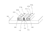
- FIG. 1 is a diagram showing a configuration of a waveguide type optical element according to the first embodiment of the present invention.
- the waveguide type optical element 10 is a Mach-Zehnder type optical modulator, which is a Mach-Zehnder (MZ) type optical waveguide 102 formed on a substrate 100, a central electrode 104 constituting a CPW type electrode, and two And ground electrodes 106 and 108.
- MZ Mach-Zehnder
- the substrate 100 is a substrate made of lithium niobate (LN) which is an electro-optic material, for example, an X-cut LN substrate.
- the MZ type optical waveguide 102 has parallel waveguides 110 and 112, and a central electrode 104 is formed in a region on the surface of the substrate 100 sandwiched between the parallel waveguides 110 and 112 in parallel with the parallel waveguides 110 and 112.
- ground electrodes 106 and 108 are formed on the side facing the center electrode 104 with the parallel waveguides 110 and 112 interposed therebetween, at positions separated from the center electrode 104 by a predetermined distance, respectively.
- the center electrode 104 and the ground electrodes 106 and 108 constitute a control electrode for controlling the light wave propagating through the parallel waveguides 110 and 112. More specifically, the center electrode 104 and the ground electrode 106 constitute a control electrode that controls light waves propagating through the parallel waveguide 110, and the center electrode 104 and the ground electrode 108 transmit light waves that propagate through the parallel waveguide 112.
- the control electrode which controls is comprised.
- the high-frequency signal is input from the lower left end of the center electrode 104, propagates toward the lower right end of the figure, and is terminated by, for example, a termination resistor (not shown) connected to the end.
- the ground electrode 106 includes a portion 106a facing the center electrode 104 (hereinafter referred to as a facing portion) 106a along the center electrode 104 and a portion 106b other than that (hereinafter referred to as a back portion). The thickness is smaller than the back portion 106b.
- the ground electrode 108 is composed of a portion 108a facing the center electrode 104 along the center electrode 104 (hereinafter referred to as a facing portion) and a portion other than that (hereinafter referred to as the back portion) 108b.
- the portion 108a is thinner than the back portion 108b.
- high-frequency signal propagation directions (that is, the length direction of the center electrode 104 and the ground electrodes 106 and 108) are respectively transmitted to the back portion 106b of the ground electrode 106 and the back portion 108b of the ground electrode 108.
- slits 116a to 116k and 118a to 118k having rectangular openings in a plan view having an opening in a direction opposite to the direction toward the central electrode 104.
- These rectangular slits 116a to 116k and 118a to 118k respectively oppose the back portion 106b of the ground electrode 106 and the back portion 108b of the ground electrode 108 along the propagation direction of the high-frequency signal.
- a plurality of interface pairs composed of two interfaces (ie, the surface of the electrode material of the corresponding ground electrode 106 or 108) are formed.
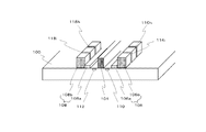
- FIG. 2 is a perspective view of a cross section taken along the line AA of the waveguide type optical element 10 shown in FIG. 1, and shows a part of the upper surface of the substrate 100 connected to the AA cross section along with the AA cross section.
- Each of the ground electrodes 106 and 108 includes a facing portion 106a, 108a facing the center electrode 104 along the center electrode 104, and a back portion 106b, 108b.
- the portions 106b and 108b are thinner than the portions 106b and 108b.
- the impedance between the center electrode 104 and the ground electrodes 106 and 108 is matched with the output impedance of a drive circuit (not shown) connected to the center electrode 104 and the ground electrodes 106 and 108.
- the facing portions 106a and 108a are formed with a thickness of 5 ⁇ m or less, for example, when the impedance is matched to 30 to 50 ⁇ .
- slits 116h and 116i, and 118h and 118i are provided in the illustrated portions of the rear portions 106b and 108b.
- 118a to 118k form a plurality of interface pairs each consisting of two interfaces that oppose each other. Each pair of these interfaces functions as a capacitor. For this reason, an additional capacitance component is added to the characteristic impedance of the distributed constant line constituted by the center electrode 104 and the ground electrodes 106 and 108, and a resonance point is generated in the S21 characteristic of the line, thereby operating in a wide band. Is possible.
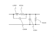
- FIG. 3 is an equivalent circuit of a distributed constant line composed of the center electrode 104 and the ground electrodes 106 and 108 in the waveguide type optical element 10 shown in FIG.
- L300 and R302 are an inductance component and a DC resistance component of the center electrode 104 and the ground electrodes 106 and 108 when the slits 116a to 116k and 118a to 118k are not provided, respectively.
- C304 and R306 are a capacitance component and an insulation resistance component between the center electrode 104 and the ground electrodes 106 and 108, respectively.
- the waveguide type optical element 10 of the present embodiment since there are slits 116a to 116k and 118a to 118k, two opposing interfaces formed by these slits function as capacitors and are added to the ground electrodes 106 and 108. A common capacitance C308 will be added in parallel. As a result, as described above, a resonance point is generated in the S21 characteristic of the distributed constant line formed by the center electrode 104 and the ground electrodes 106 and 108, and a broadband operation is possible.
- the slits 116a to 116k and 118a to 118k are preferably arranged periodically at regular intervals, but may be arranged non-periodically at irregular intervals.
- an electrode configuration does not generate additional stress on the substrate 100, it is effectively applied even when the thickness of the substrate 100 is set to 4 ⁇ m or less, for example, for speed matching between the light wave and the high frequency. Is possible.
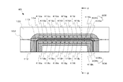
- FIG. 4 is a diagram showing a configuration of a waveguide type optical element according to the second embodiment of the present invention.
- the same reference numerals as those in FIGS. 1 and 2 are used for the same constituent elements as those of the waveguide type optical element 10 according to the first embodiment shown in FIGS.
- the description of the waveguide type optical element 10 according to the first embodiment described above is incorporated.
- the present waveguide type optical element 40 has the same configuration as the waveguide type optical element 10 according to the first embodiment, but includes ground electrodes 406 and 408 instead of the ground electrodes 106 and 108.
- the ground electrodes 406 and 408 have the same configuration as that of the ground electrodes 106 and 108, except that the opposed portions 406a and 408a and the rear portions 406b and 408b are used instead of the opposed portions 106a and 108a and the rear portions 106b and 108b.
- the facing portions 406a and 408a and the back portions 406b and 408b have the same configuration as the facing portions 106a and 108a and the back portions 106b and 108b.
- the opposing portions 406a and 408a have a plan view having openings in the direction toward the center electrode 104 along the propagation direction of the high-frequency signal (that is, the length direction of the center electrode 104 and the ground electrodes 406 and 408), respectively. Rectangular slits 416a to 416k and 418a to 418k are provided.
- the rectangular slits 416a to 416k and 418a to 418k respectively oppose the opposing portion 406a of the ground electrode 406 and the opposing portion 408a of the ground electrode 408 along the propagation direction of the high-frequency signal.
- a plurality of interface pairs composed of two interfaces ie, the surface of the corresponding ground electrode 406 or 408 electrode material) are formed.
- FIG. 5 is a perspective view of a cross section taken along the line BB of the waveguide type optical element 40 shown in FIG. 4, showing a part of the upper surface of the substrate 100 connected to the BB cross section along with the BB cross section.
- Each of the ground electrodes 406 and 408 includes a facing portion 406a and 408a facing the center electrode 104 along the center electrode 104, and a back portion 406b and 408b.
- the facing portions 406a and 408a are formed to be thinner than the back portions 406b and 408b.
- the impedance between the center electrode 104 and the ground electrodes 406 and 408 is matched with the output impedance of a drive circuit (not shown) connected to the center electrode 104 and the ground electrodes 406 and 408.
- the facing portions 406a and 408a are formed with a thickness of 5 ⁇ m or less, for example, when the impedance is matched to 30 to 50 ⁇ .
- slits 418g, 418h, and 418i are provided in the illustrated portion of the facing portion 408a.
- 418a to 418k form a plurality of interface pairs each composed of two opposing interfaces. Each pair of these interfaces functions as a capacitor.
- an additional capacitance component is added to the characteristic impedance of the distributed constant line formed by the center electrode 104 and the ground electrodes 406 and 408. It will be. Furthermore, a resonance point is generated in the S21 characteristic of the line, and a broadband operation is possible.
- the slits 416a to 416k and 418a to 418k are desirably arranged periodically at regular intervals, but may be arranged irregularly at irregular intervals.
- an electrode configuration does not generate additional stress on the substrate 100, it is effectively applied even when the thickness of the substrate 100 is set to 4 ⁇ m or less, for example, for speed matching between the light wave and the high frequency. Is possible.
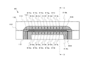
- FIG. 6 is a diagram showing a configuration of a waveguide type optical device according to the third embodiment of the present invention. 6 and FIG. 7 to be described later, the same reference numerals as those in FIGS. 1 and 2 are used for the same constituent elements as those of the waveguide type optical element 10 according to the first embodiment shown in FIGS. The description of the waveguide type optical element 10 according to the first embodiment described above is incorporated.
- the waveguide type optical element 60 has the same configuration as the waveguide type optical element 10 according to the first embodiment, but includes ground electrodes 606 and 608 instead of the ground electrodes 106 and 108.
- the ground electrodes 606 and 608 have the same configuration as the ground electrodes 106 and 108. However, it differs in that it has opposed portions 606a, 608a and rear portions 606b, 608b instead of the opposed portions 106a, 108a and the back portions 106b, 108b.
- the facing portions 606a and 608a and the back portions 606b and 608b have the same configuration as the facing portions 106a and 108a and the back portions 106b and 108b.
- the back portions 606b and 608b each have an opening toward the center electrode 104 along the propagation direction of the high-frequency signal (that is, the length direction of the center electrode 104 and the ground electrodes 606 and 608). Slits 616a to 616k and 618a to 618k that are rectangular in view are provided.
- These rectangular slits 616a to 616k and 618a to 618k respectively oppose the back portion 606b of the ground electrode 606 and the back portion 608b of the ground electrode 608 along the propagation direction of the high-frequency signal.
- a plurality of interface pairs composed of two interfaces (ie, the surface of the electrode material of the corresponding ground electrode 606 or 608) are formed.
- FIG. 7 is a perspective view of a cross section taken along the CC arrow of the waveguide type optical element 60 shown in FIG. 6, showing a part of the upper surface of the substrate 100 connected to the CC cross section along with the CC cross section.
- Each of the ground electrodes 606 and 608 includes a facing portion 606a and 608a facing the center electrode 104 along the center electrode 104, and a back portion 606b and 608b, and the facing portions 606a and 608a are the back of the back.
- the portions 606b and 608b are thinner than the portions 606b and 608b.
- the impedance between the center electrode 104 and the ground electrodes 606 and 608 is matched with the output impedance of a drive circuit (not shown) connected to the center electrode 104 and the ground electrodes 606 and 608.
- the facing portions 606a and 608a are formed with a thickness of 5 ⁇ m or less, for example, when the impedance is matched to 30 to 50 ⁇ .
- slits 616g, 616h, 616i and 618g, 618h, 618i are provided in the illustrated portions of the rear portions 606b, 608b.
- 618a to 618k form a plurality of interface pairs each composed of two opposing interfaces. Each pair of these interfaces functions as a capacitor.
- an additional capacitance component is added to the characteristic impedance of the distributed constant line constituted by the center electrode 104 and the ground electrodes 606 and 608. .
- a resonance point is generated in the S21 characteristic of the line, and a broadband operation is possible.
- the slits 616a to 616k and 618a to 618k are desirably arranged periodically at regular intervals, but may be arranged irregularly at irregular intervals.
- an electrode configuration does not generate additional stress on the substrate 100, it is effectively applied even when the thickness of the substrate 100 is set to 4 ⁇ m or less, for example, for speed matching between the light wave and the high frequency. Is possible.
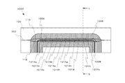
- FIG. 8 is a diagram showing a configuration of a waveguide type optical device according to the fourth embodiment of the present invention.
- the same reference numerals as those in FIGS. 1 and 2 are used for the same constituent elements as those of the waveguide type optical element 10 according to the first embodiment shown in FIGS.
- the description of the waveguide type optical element 10 according to the first embodiment described above is incorporated.
- the waveguide type optical element 80 has the same configuration as the waveguide type optical element 10 according to the first embodiment, but instead of the ground electrodes 106 and 108, a ground electrode having a certain uniform thickness is provided. 806 and 808 are provided. The ground electrodes 806 and 808 are respectively provided in the depth direction (thickness direction) of the ground electrodes 806 and 808 along the propagation direction of the high-frequency signal (that is, the length direction of the center electrode 104 and the ground electrodes 806 and 808). Are provided with rectangular trenches 816a to 816k and 818a to 818k.
- the ground electrodes 806 and 808 are respectively opposed to two interfaces (that is, the corresponding ground electrode 806 or A plurality of interface pairs formed of 808 electrode material surface).
- FIG. 9 is a perspective view of a cross section taken along the arrow DD of the waveguide type optical element 80 shown in FIG. A part of the upper surface of the substrate 100 connected to the DD cross section is shown together with the DD cross section.
- the illustrated portions of the ground electrodes 806 and 808 are provided with trenches 816g, 816h, 816i and 818g, 818h, 818i.
- the waveguide type optical element 80 having the above-described configuration, two rectangular trenches 816a to 816k and 818a to 818k respectively provided in the ground electrodes 806 and 808 along the propagation direction of the high-frequency signal are opposed to each other. A plurality of interface pairs formed by the interfaces are formed. Each pair of these interfaces functions as a capacitor. For this reason, as in the waveguide type optical element 10 according to the first embodiment, an additional capacitance component is added to the characteristic impedance of the distributed constant line formed by the center electrode 104 and the ground electrodes 806 and 808. As a result, a resonance point is generated in the S21 characteristic of the line, and a broadband operation is possible.
- the trenches 816a to 816k and 818a to 818k are desirably arranged periodically at regular intervals, but may be arranged non-periodically at irregular intervals.
- an electrode configuration does not generate additional stress on the substrate 100, it is effectively applied even when the thickness of the substrate 100 is set to 4 ⁇ m or less, for example, for speed matching between the light wave and the high frequency. Is possible.
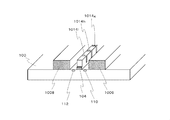
- FIG. 10 is a diagram showing the configuration of a waveguide optical device according to the fifth embodiment of the present invention.
- the same reference numerals as those in FIGS. 1 and 2 are used for the same components as those of the waveguide type optical element 10 according to the first embodiment shown in FIGS.
- the description of the waveguide type optical element 10 according to the first embodiment described above is incorporated.
- the waveguide type optical element 1000 has the same configuration as the waveguide type optical element 10 according to the first embodiment, but instead of the ground electrodes 106 and 108, a ground electrode having a certain uniform thickness is provided. 1006 and 1008 are provided, and instead of the center electrode 104, a center electrode 1004 is provided.
- the center electrode 1004 has a high-frequency signal propagation direction (that is, the length direction of the center electrode 1004 and the ground electrodes 1006 and 1008) above the center electrode 1004 (a direction away from the substrate 100, that is, the paper surface of FIG. 10). Rectangular slits 1014a to 1014k opened in the front direction) are provided.
- the center electrode 1004 has a plurality of surfaces that are opposed to each other (that is, the surface of the electrode material of the center electrode 1004) along the propagation direction of the high-frequency signal. A pair of interfaces is formed.
- FIG. 11 is a perspective view of the waveguide optical element 1000 shown in FIG. 10 taken along the EE arrow, showing a part of the upper surface of the substrate 100 connected to the EE cross section along with the EE cross section.
- Ground electrodes 1006 and 1008 having a uniform thickness and a center electrode 1004 are provided, and slits 1014g, 1014h, and 1014i are provided in the illustrated portion of the center electrode 1004.
- a plurality of rectangular interfaces 1014a to 1014k provided in the center electrode 1004 along the propagation direction of the high-frequency signal are each composed of a plurality of interfaces opposed to each other.
- a pair of interfaces is formed.
- Each pair of these interfaces functions as a capacitor.
- the slits 1014a to 1014k are desirably arranged periodically at regular intervals, but may be arranged irregularly at irregular intervals.
- an electrode configuration does not generate additional stress on the substrate 100, it is effectively applied even when the thickness of the substrate 100 is set to 4 ⁇ m or less, for example, for speed matching between the light wave and the high frequency. Is possible.
- FIG. 12 is a diagram showing a configuration of a waveguide type optical device according to the sixth embodiment of the present invention.
- FIG. 12 and FIG. 13 to be described later the same reference numerals as those in FIGS. 1 and 2 are used for the same constituent elements as those of the waveguide type optical element 10 according to the first embodiment shown in FIGS. The description of the waveguide type optical element 10 according to the first embodiment described above is incorporated.
- the waveguide type optical element 1200 has the same configuration as the waveguide type optical element 10 according to the first embodiment, but includes ground electrodes 1206 and 1208 instead of the ground electrodes 106 and 108.
- the ground electrodes 1206 and 1208 have the same configuration as the ground electrodes 106 and 108, except that they have opposed portions 1206a and 1208a and rear portions 1206b and 1208b instead of the opposed portions 106a and 108a and the back portions 106b and 108b.
- the facing portions 1206a and 1208a and the back portions 1206b and 1208b have the same configuration as the facing portions 106a and 108a and the back portions 106b and 108b.
- the rear portions 1206b and 1208b are not provided with slits, and the opposing portions 1206a and 1208a are each along the propagation direction of the high-frequency signal (that is, the length direction of the center electrode 104 and the ground electrodes 1206 and 1208).
- slits 1216a to 1216k and 1218a to 1218k having openings toward the center electrode 104 are provided.
- the slits 1216a to 1216k and 1218a to 1218k are within a predetermined distance in the direction away from the center electrode 104 from the edge closer to the center electrode 104 of the opposing portions 1206a and 1208a of the ground electrodes 1206 and 1208, respectively. In the opening, the width is narrower than that of the other portions.
- the opposing portion 1206a of the ground electrode 406 and the opposing portion 1208a of the ground electrode 1208 respectively oppose each other along the propagation direction of the high-frequency signal.
- a plurality of interface pairs composed of two interfaces ie, the surface of the electrode material of the corresponding ground electrode 1206 or 1208, are formed.
- FIG. 13 is a perspective view of a cross-section taken along the FF arrow of the waveguide type optical element 1200 shown in FIG. 12, showing a part of the upper surface of the substrate 100 connected to the FF cross section along with the FF cross section.
- Each of the ground electrodes 1206 and 1208 includes a facing portion 1206a and 1208a facing the center electrode 104 along the center electrode 104, and a back portion 1206b and 1208b.
- the facing portions 1206a and 1208a are formed to be thinner than the back portions 1206b and 1208b.
- the impedance between the center electrode 104 and the ground electrodes 1206 and 1208 is matched with the output impedance of a drive circuit (not shown) connected to the center electrode 104 and the ground electrodes 1206 and 1208.
- the facing portions 1206a and 1208a are formed with a thickness of, for example, 5 ⁇ m or less when the impedance is matched to 30 to 50 ⁇ .
- slits 1218h and 1218i are provided in the illustrated portion of the facing portion 1208a.
- rectangular slits 1216a to 1216k respectively provided in the facing portion 1206a of the ground electrode 1206 and the facing portion 1208a of the ground electrode 1208 along the propagation direction of the high-frequency signal.
- 1218a to 1218k form a plurality of interface pairs each composed of two opposing interfaces. Each pair of these interfaces functions as a capacitor.
- an additional capacitance component is added to the characteristic impedance of the distributed constant line formed by the center electrode 104 and the ground electrodes 1206 and 1208. As a result, a resonance point is generated in the S21 characteristic of the line, and a broadband operation is possible.
- the slits 1216a to 1216k and 1218a to 1218k are directions away from the center electrode 104 from the edges of the opposing portions 1206a and 1208a of the ground electrodes 1206 and 1208 closer to the center electrode 104, respectively.
- the width is narrower than the other portions. That is, each of the slits 1216a to 1216k and 1218a to 1218k constitutes a C-shaped loop with the corresponding back portions 1206b and 1208b on the back.
- Each of the C-shaped loops functions as a coil (inductance), and an additional inductance component is added to the characteristic impedance of the distributed constant line formed by the center electrode 104 and the ground electrodes 1206 and 1208, and the line The propagation speed of the high frequency which propagates is made slow.
- FIG. 14 is an equivalent circuit of a distributed constant line composed of the center electrode 104 and the ground electrodes 1206 and 1208 in the waveguide type optical element 1200 shown in FIG. L1400 and R1402 are inductance components and resistance components of the center electrode 104 and the ground electrodes 1206 and 1208, respectively, when there are no slits 1216a to 1216k and 1218a to 1218k.
- C1404 and R1406 are a capacitance component and a resistance component between the center electrode 104 and the ground electrodes 1206 and 1208, respectively.
- the waveguide element 10 of the present embodiment since there are slits 1216a to 1216k and 1218a to 1218k, two opposing interfaces formed by these slits function as capacitors. An additional capacitance C1408 will be added in parallel to the ground electrodes 1206, 1208. *
- each of the slits 1216a to 1216k and 1218a to 1218k functions as a coil with a C-shaped shape, and an additional inductance L1410 is added in series to the ground electrodes 1206 and 1208.
- the propagation speed of the high frequency propagating through the distributed constant line constituted by the center electrode 104 and the ground electrodes 1206 and 1208 becomes slow.
- the high-frequency propagation speed is adjusted by adjusting the shape and dimensions of the ground electrodes (1206, 1208) so as to compete with this. Therefore, the degree of freedom in design as a whole of the waveguide type optical device is improved.
- the S21 characteristic can be widened by changing the distributed constant line formed by the center electrode 104 and the ground electrodes 106 and 108.
- the slits 1216a to 1216k and 1218a to 1218k are desirably arranged periodically at regular intervals, but may be arranged irregularly at irregular intervals.
- an electrode configuration does not generate additional stress on the substrate 100, it is effectively applied even when the thickness of the substrate 100 is set to 4 ⁇ m or less, for example, for speed matching between the light wave and the high frequency. Is possible.
- the center electrode (such as 104) or the ground electrode (such as 106) extends along the propagation direction of the high-frequency signal.
- the center electrode (such as 104) or the ground electrode (such as 106) extends along the propagation direction of the high-frequency signal.
- slits (116a, etc.) and trenches (816a, etc.) a plurality of interface pairs each formed of two interfaces that oppose each other are formed. Since each of these interface pairs functions as a capacitor, a resonance point is generated in the S21 characteristic of the distributed constant line composed of the center electrode and the ground electrode.
- the waveguide-type optical element is further improved. Broadband operation is possible.
Landscapes
- Physics & Mathematics (AREA)
- Nonlinear Science (AREA)
- General Physics & Mathematics (AREA)
- Optics & Photonics (AREA)
- Chemical & Material Sciences (AREA)
- Engineering & Computer Science (AREA)
- Ceramic Engineering (AREA)
- Crystallography & Structural Chemistry (AREA)
- Electromagnetism (AREA)
- Optical Modulation, Optical Deflection, Nonlinear Optics, Optical Demodulation, Optical Logic Elements (AREA)
- Optical Integrated Circuits (AREA)
Abstract
導波路型光素子において、更なる広帯域動作を可能とする。 電気光学効果を有する基板(100)上に形成された光導波路(110、112)と、当該光導波路を伝搬する光波を制御する制御電極と、を備える導波路型光素子であって、 前記制御電極は、前記光導波路に対し平行に形成された中心電極(104)と、当該中心電極導体を所定の距離だけ隔てて前記基板の面方向において挟むように形成された接地電極(106、108)と、で構成され、前記中心電極又は前記接地電極は、当該中心電極及び当該接地電極を伝搬する高周波信号の伝搬方向に沿って、それぞれが相対抗する2つの界面で構成される複数の界面のペアが形成されている。
Description
本発明は、光導波路と当該光導波路を伝搬する光波を制御するための制御電極とを備えた導波路型光素子に関し、特に、広い周波数範囲に亘って動作が可能な広帯域導波路型光素子に関する。
近年、光通信や光計測の分野においては、電気光学効果を有する基板上に光導波路を形成した光変調器などの導波路型光素子が多く用いられている。導波路型光素子は、一般に、上記光導波路と、当該光導波路内を伝搬する光波を制御するための制御電極を備える。
このような導波路型光素子として、例えば強誘電体結晶であるニオブ酸リチウム(LiNbO3)(「LN」とも称する)を基板に用いたマッハツェンダ型光変調器が広く用いられている。マッハツェンダ型光変調器は、外部から光を導入するための入射導波路と、当該入射導波路により導入された光を2つの経路に分けて伝搬させるための分岐部と、分岐部の後段に分岐されたそれぞれの光を伝搬させる2本の並行導波路と、当該2本の並行導波路を伝搬した光を合波して外部へ出力するための出射導波路とにより構成されるマッハツェンダ型光導波路を備える。
また、マッハツェンダ型光変調器は、電圧を印加することで、電気光学効果を利用して、上記並行導波路内を伝搬する光波の位相を変化させて制御するための制御電極を備える。当該制御電極は、一般に、上記並行導波路の長さ方向に沿ってその上部又はその近傍に形成された中心電極と、当該中心電極に離間して配置された接地電極と、を有するCPW(Coplanar Waveguide)型電極として構成されている。
特に、並行導波路を伝搬する光波をより高い周波数で制御する広帯域(マイクロ波帯域)のマッハツェンダ型光変調器の設計においては、以下(1)~(3)をバランスさせる必要がある。
(1)並行導波路を伝搬する光の伝搬速度と中心電極を伝搬する伝搬速度との速度整合(以下、単に「速度整合」という)
(2)駆動回路の出力インピーダンスに対する中心電極の入力インピーダンスの整合(以下、インピーダンス整合という)
(3)光波とマイクロ波との重なり(変調効率)
(1)並行導波路を伝搬する光の伝搬速度と中心電極を伝搬する伝搬速度との速度整合(以下、単に「速度整合」という)
(2)駆動回路の出力インピーダンスに対する中心電極の入力インピーダンスの整合(以下、インピーダンス整合という)
(3)光波とマイクロ波との重なり(変調効率)
すなわち、マッハツェンダ型光変調器では、速度整合と、インピーダンス整合と、を行うことを必須要件として、でき得る限り駆動電圧を低減する必要がある。さらに、広帯域化のためには、電極を伝搬する高周波信号の損失(マイクロ波損失)を低減することも必要となる。しかしながら、駆動電圧の低減と広帯域化は相反的な関係にあり、駆動電圧の増加を伴うことなく広帯域化を図ることには困難を伴う。
従来、速度整合とインピーダンス整合を両立させるため基板の表面をリッジ形状に加工し、駆動電圧の上昇を抑制しつつ広帯域化を図ることが知られている(非特許文献1)。
また、更なる広帯域化のため、接地電極及び又は中心電極を2段構成(すなわち、それら電極の厚さを2段階に変化させる構成)としてインピーダンスを変えずに速度整合を満たす電極の厚さを厚くすることで、マイクロ波の導体損失を低減させている(特許文献1)
また、更なる広帯域化のため、接地電極及び又は中心電極を2段構成(すなわち、それら電極の厚さを2段階に変化させる構成)としてインピーダンスを変えずに速度整合を満たす電極の厚さを厚くすることで、マイクロ波の導体損失を低減させている(特許文献1)
上記従来の導波路型光素子では、基板厚さや電極厚さ等により速度整合を図りつつマイクロ波損失を低減して、ある程度まで広帯域な動作が可能となっている。しかしながら、実際上、形成できる電極の厚さは50μm程度が上限であり、電極厚さを厚くすることで広帯域化を図るには限界がある。すなわち、電極形成の際には、形成すべき電極の厚さに応じて電極のパターンニングに用いるレジストも厚く形成する必要がある。しかし、レジスト厚さが厚くなるにつれてレジスト内部の応力が高まり、レジストと基板との間の付着力が低下して、電極形成途中でレジストが剥離してしまう確率が高まる。また、厚さに応じて電極形成の時間も長くなり、生産性が低下する。ここで、電極の形成方法は、非特許文献1、2に記載されているように、フォトレジスト及び電気メッキを用いたセミアディテイブを用いている。
"Broadband Optical Modulators"、ISBN978-1-4398-2506-8
"A review of lithium niobate modulators for fiber-optic communications systems"、Selected Topics in Quantum Electronics, IEEE Journal of, 2000, Vol.6.No.1:pp 69-82
上記背景より、導波路型光素子において、更なる広帯域動作を可能とするため構成の実現が望まれている。
本発明の一の態様は、電気光学効果を有する基板上に形成された光導波路と、当該光導波路を伝搬する光波を制御する制御電極と、を備える導波路型光素子であって、前記制御電極は、前記光導波路に沿って形成された中心電極と、当該中心電極導体から所定の距離だけ隔てて前記基板の面方向において挟むように形成された接地電極と、で構成され、前記中心電極又は前記接地電極は、当該中心電極及び当該接地電極を伝搬する高周波信号の伝搬方向に沿って、それぞれが相対抗する2つの界面で構成される複数の界面のペアが形成されている。
本発明の他の態様によると、前記複数の界面のペアは、前記高周波の伝搬方向に沿って所定の間隔で周期的に形成されている。
本発明の他の態様によると、前記接地電極は、前記中心電極に沿って当該中心電極と対向する部分が、他の部分よりも厚さが薄く形成されており、前記複数の界面のペアは、前記厚さが薄く形成された前記接地電極の部分以外の部分に形成されている。
本発明の他の態様によると、前記複数の界面のペアは、前記中心電極に向かう方向とは逆の方向に向かって開口を有する矩形のスリットとして形成されている。
本発明の他の態様によると、前記複数の界面のペアは、前記中心電極に向かう方向に開口を有する矩形のスリットとして形成されている。
本発明の他の態様によると、前記接地電極は、前記中心電極に沿って当該中心電極と対向する部分が、他の部分よりも厚さが薄く形成されており、前記複数の界面のペアは、前記厚さが薄く形成された前記接地電極の部分に形成されている。
本発明の他の態様によると、前記複数の界面のペアは、前記中心電極の方向に向かって開口を有する矩形のスリットとして形成されている。
本発明の他の態様によると、前記矩形のスリットは、前記接地電極の前記中心電極に近い側のエッジから当該中心電極から離れる方向に所定の距離以内の範囲にわたり、当該範囲以外の部分よりも幅が狭く形成されている。
本発明の他の態様によると、前記複数の界面のペアは、前記接地電極の深さ方向に設けられた矩形の穴として形成されている。
本発明の他の態様によると、前記複数の界面のペアは、前記中心電極の深さ方向に設けられたスリットとして形成されている。
本発明の他の態様によると、前記基板は、ニオブ酸リチウムで構成されており、前記厚さが薄く形成された前記接地電極の部分の厚さは、5μm以下である。
本発明の他の態様によると、前記基板は、ニオブ酸リチウムで構成されており、前記基板の厚さは4μm以下である。
本発明の他の態様によると、前記複数の界面のペアは、前記高周波の伝搬方向に沿って所定の間隔で周期的に形成されている。
本発明の他の態様によると、前記接地電極は、前記中心電極に沿って当該中心電極と対向する部分が、他の部分よりも厚さが薄く形成されており、前記複数の界面のペアは、前記厚さが薄く形成された前記接地電極の部分以外の部分に形成されている。
本発明の他の態様によると、前記複数の界面のペアは、前記中心電極に向かう方向とは逆の方向に向かって開口を有する矩形のスリットとして形成されている。
本発明の他の態様によると、前記複数の界面のペアは、前記中心電極に向かう方向に開口を有する矩形のスリットとして形成されている。
本発明の他の態様によると、前記接地電極は、前記中心電極に沿って当該中心電極と対向する部分が、他の部分よりも厚さが薄く形成されており、前記複数の界面のペアは、前記厚さが薄く形成された前記接地電極の部分に形成されている。
本発明の他の態様によると、前記複数の界面のペアは、前記中心電極の方向に向かって開口を有する矩形のスリットとして形成されている。
本発明の他の態様によると、前記矩形のスリットは、前記接地電極の前記中心電極に近い側のエッジから当該中心電極から離れる方向に所定の距離以内の範囲にわたり、当該範囲以外の部分よりも幅が狭く形成されている。
本発明の他の態様によると、前記複数の界面のペアは、前記接地電極の深さ方向に設けられた矩形の穴として形成されている。
本発明の他の態様によると、前記複数の界面のペアは、前記中心電極の深さ方向に設けられたスリットとして形成されている。
本発明の他の態様によると、前記基板は、ニオブ酸リチウムで構成されており、前記厚さが薄く形成された前記接地電極の部分の厚さは、5μm以下である。
本発明の他の態様によると、前記基板は、ニオブ酸リチウムで構成されており、前記基板の厚さは4μm以下である。
以下、図面を参照して、本発明の実施の形態を説明する。以下に示す実施形態は、マッハツェンダ型光導波路で構成される光変調器である。しかし、本発明に係る導波路型光素子は、これに限らず、CPW型電極を構成する制御電極により動作するマッハツェンダ型光導波路、方向性結合器型光導波路、Y分岐型光導波路、その他のタイプの光導波路で構成された光変調器、光スイッチ、その他の機能を有する導波路型光素子に、一般に適用することができる。
〔第1実施形態〕
まず、本発明の第1の実施形態について説明する。
図1は、本発明の第1の実施形態に係る導波路型光素子の構成を示す図である。
本導波路型光素子10は、マッハツェンダ型光変調器であり、基板100上に形成されたマッハツェンダ(MZ、Mach-Zehnder)型光導波路102と、CPW型電極を構成する中心電極104及び2つの接地電極106、108と、を有する。
まず、本発明の第1の実施形態について説明する。
図1は、本発明の第1の実施形態に係る導波路型光素子の構成を示す図である。
本導波路型光素子10は、マッハツェンダ型光変調器であり、基板100上に形成されたマッハツェンダ(MZ、Mach-Zehnder)型光導波路102と、CPW型電極を構成する中心電極104及び2つの接地電極106、108と、を有する。
基板100は、電気光学材料であるニオブ酸リチウム(LN)から成る基板であり、例えばXカットのLN基板である。MZ型光導波路102は、並行導波路110、112を有し、並行導波路110、112に挟まれた基板100面上の領域に、当該並行導波路110、112と平行に中心電極104が形成されている。また、並行導波路110、112を挟んで中心電極104と対向する側に、それぞれ、中心電極104から所定の距離だけ離れた位置に、接地電極106、108が形成されている。これらの中心電極104、接地電極106、108は、並行導波路110、112を伝搬する光波を制御する制御電極を構成する。より詳細には、中心電極104と接地電極106とが、並行導波路110を伝搬する光波を制御する制御電極を構成し、中心電極104と接地電極108とが、並行導波路112を伝搬する光波を制御する制御電極を構成している。
高周波信号は、中心電極104の図示左下側の端部から入力され、図示右下側端部に向かって伝搬して、例えば当該端部に接続された終端抵抗(不図示)により終端される。
接地電極106は、中心電極104に沿って当該中心電極104と対向する部分(以下、対向部分)106aと、それ以外の部分(以下、後背部分)106bとで構成されており、対向部分106aは、後背部分106bよりも厚さが薄くなっている。同様に、接地電極108は、中心電極104に沿って当該中心電極104と対向する部分(以下、対向部分)108aと、それ以外の部分(以下、後背部分)108bとで構成されており、対向部分108aは、後背部分108bよりも厚さが薄くなっている。
特に、本実施形態では、接地電極106の後背部分106bと、接地電極108の後背部分108bとに、それぞれ、高周波信号の伝搬方向(すなわち、中心電極104、接地電極106、108の長さ方向)に沿って、中心電極104に向かう方向とは逆の方向に向かって開口を有する平面視が矩形のスリット116a~116k、118a~118kが設けられている。これらの矩形のスリット116a~116k、118a~118kにより、接地電極106の後背部分106bと、接地電極108の後背部分108bとには、それぞれ、高周波信号の伝搬方向に沿って、それぞれが相対抗する2つの界面(すなわち、対応する接地電極106又は108の電極材料の表面)で構成される複数の界面のペアが形成される。
図2は、図1に示す導波路型光素子10のAA矢視断面の斜視図であり、AA断面と共に当該AA断面につながる基板100の上面の一部が示されている。接地電極106及び108は、それぞれ、中心電極104に沿って当該中心電極104と対向する対向部分106a、108aと、後背部分106b、108bとで構成されており、対向部分106a、108aは、当該後背部分106b、108bよりも厚さが薄く形成されている。これにより、中心電極104と接地電極106、108とのインピーダンスが、当該中心電極104、接地電極106、108に接続される駆動回路(不図示)の出力インピーダンスと整合される。対向部分106a、108aは、上記インピーダンスを30~50Ωに整合する場合には、例えば5μm以下の厚さで形成される。また、後背部分106b、108bの図示部分には、スリット116h、116i、及び118h、118iが設けられている。
上記の構成を有する導波路型光素子10では、高周波信号の伝搬方向に沿って、接地電極106の後背部分106bと、接地電極108の後背部分108bとにそれぞれ設けられた矩形のスリット116a~116k、118a~118kにより、それぞれが相対抗する2つの界面で構成される複数の界面のペアが形成される。これらの界面のペアが、それぞれコンデンサとして機能する。このため、中心電極104と接地電極106、108とにより構成される分布定数線路の特性インピーダンスに付加的な容量成分が追加されることとなり、当該線路のS21特性に共鳴点が生じて、広帯域動作が可能となる。
図3は、図1に示す導波路型光素子10における、中心電極104と接地電極106、108とにより構成される分布定数線路の等価回路である。L300、R302は、それぞれ、スリット116a~116k、118a~118kがない場合の、中心電極104、接地電極106、108のインダクタンス成分及び直流抵抗成分である。C304、R306は、それぞれ、中心電極104と接地電極106、108との間のキャパシタンス成分及び絶縁抵抗成分である。本実施形態の導波路型光素子10では、スリット116a~116k、118a~118kがあることにより、これらのスリットが構成する相対抗する2つの界面がコンデンサとして機能し、接地電極106、108に付加的なキャパシタンスC308が、並列に追加されることとなる。これにより、上述のように、中心電極104と接地電極106、108とにより構成される分布定数線路のS21特性に共鳴点が生じ、広帯域動作が可能となる。
なお、スリット116a~116k、118a~118kは、等間隔で周期的に配されていることが望ましいが、不等間隔で非周期的に配するものとしてもよい。また、このような電極構成は、基板100に付加的な応力を発生させないため、光波と高周波との間の速度整合のために基板100の厚さを例えば4μm以下とした場合にも有効に適用することが可能である。
〔第2実施形態〕
次に、本発明の第2の実施形態について説明する。
図4は、本発明の第2の実施形態に係る導波路型光素子の構成を示す図である。なお、図4及び後述する図5においては、図1及び図2に示す第1の実施形態に係る導波路型光素子10と同じ構成要素については、図1及び図2と同じ符号を用いるものとし、上述した第1の実施形態に係る導波路型光素子10における説明を援用するものとする。
次に、本発明の第2の実施形態について説明する。
図4は、本発明の第2の実施形態に係る導波路型光素子の構成を示す図である。なお、図4及び後述する図5においては、図1及び図2に示す第1の実施形態に係る導波路型光素子10と同じ構成要素については、図1及び図2と同じ符号を用いるものとし、上述した第1の実施形態に係る導波路型光素子10における説明を援用するものとする。
本導波路型光素子40は、第1の実施形態に係る導波路型光素子10と同様の構成を有するが、接地電極106、108に代えて、接地電極406、408を備える。接地電極406、408は、接地電極106、108と同様の構成を有するが、対向部分106a、108a及び後背部分106b、108bに代えて、対向部分406a、408a及び後背部分406b、408bを有する点が異なる。対向部分406a、408a及び後背部分406b、408bは、対向部分106a、108a及び後背部分106b、108bと同様の構成を有する。しかし、後背部分406b、408bにスリットが設けられていない。対向部分406a、408aに、それぞれ、高周波信号の伝搬方向(すなわち、中心電極104、接地電極406、408の長さ方向)に沿って、中心電極104に向かう方向に向かって開口を有する平面視が矩形のスリット416a~416k、418a~418kが設けられている。
これらの矩形のスリット416a~416k、418a~418kにより、接地電極406の対向部分406aと、接地電極408の対向部分408aとには、それぞれ、高周波信号の伝搬方向に沿って、それぞれが相対抗する2つの界面(すなわち、対応する接地電極406又は408の電極材料の表面)で構成される複数の界面のペアが形成される。
図5は、図4に示す導波路型光素子40のBB矢視断面の斜視図であり、BB断面と共に当該BB断面につながる基板100の上面の一部が示されている。接地電極406及び408は、それぞれ、中心電極104に沿って当該中心電極104と対向する対向部分406a、408aと、後背部分406b、408bとで構成されている。対向部分406a、408aは、当該後背部分406b、408bよりも厚さが薄く形成されている。これにより、中心電極104と接地電極406、408とのインピーダンスが、当該中心電極104、接地電極406、408に接続される駆動回路(不図示)の出力インピーダンスと整合される。対向部分406a、408aは、上記インピーダンスを30~50Ωに整合する場合には、例えば5μm以下の厚さで形成される。また、対向部分408aの図示部分には、スリット418g、418h、418iが設けられている。
上記の構成を有する導波路型光素子40では、高周波信号の伝搬方向に沿って、接地電極406の対向部分406aと、接地電極408の対向部分408aとにそれぞれ設けられた矩形のスリット416a~416k、418a~418kにより、それぞれが相対抗する2つの界面で構成される複数の界面のペアが形成される。これらの界面のペアが、それぞれコンデンサとして機能する。このため、第1の実施形態に係る導波路型光素子10と同様に、中心電極104と接地電極406、408とにより構成される分布定数線路の特性インピーダンスに付加的な容量成分が追加されることとなる。さらに、当該線路のS21特性に共鳴点が生じて、広帯域動作が可能となる。
なお、スリット416a~416k、418a~418kは、等間隔で周期的に配することが望ましいが、不等間隔で非周期的に配するものとしてもよい。また、このような電極構成は、基板100に付加的な応力を発生させないため、光波と高周波との間の速度整合のために基板100の厚さを例えば4μm以下とした場合にも有効に適用することが可能である。
〔第3実施形態〕
次に、本発明の第3の実施形態について説明する。
図6は、本発明の第3の実施形態に係る導波路型光素子の構成を示す図である。なお、図6及び後述する図7においては、図1及び図2に示す第1の実施形態に係る導波路型光素子10と同じ構成要素については、図1及び図2と同じ符号を用いるものとし、上述した第1の実施形態に係る導波路型光素子10における説明を援用するものとする。
次に、本発明の第3の実施形態について説明する。
図6は、本発明の第3の実施形態に係る導波路型光素子の構成を示す図である。なお、図6及び後述する図7においては、図1及び図2に示す第1の実施形態に係る導波路型光素子10と同じ構成要素については、図1及び図2と同じ符号を用いるものとし、上述した第1の実施形態に係る導波路型光素子10における説明を援用するものとする。
本導波路型光素子60は、第1の実施形態に係る導波路型光素子10と同様の構成を有するが、接地電極106、108に代えて、接地電極606、608を備える。接地電極606、608は、接地電極106、108と同様の構成を有する。しかし、対向部分106a、108a及び後背部分106b、108bに代えて、対向部分606a、608a及び後背部分606b、608bを有する点が異なる。対向部分606a、608a及び後背部分606b、608bは、対向部分106a、108a及び後背部分106b、108bと同様の構成を有する。しかし、後背部分606b、608bに、それぞれ、高周波信号の伝搬方向(すなわち、中心電極104、接地電極606、608の長さ方向)に沿って、中心電極104に向かう方向に向かって開口を有する平面視が矩形のスリット616a~616k、618a~618kが設けられている。
これらの矩形のスリット616a~616k、618a~618kにより、接地電極606の後背部分606bと、接地電極608の後背部分608bとには、それぞれ、高周波信号の伝搬方向に沿って、それぞれが相対抗する2つの界面(すなわち、対応する接地電極606又は608の電極材料の表面)で構成される複数の界面のペアが形成される。
図7は、図6に示す導波路型光素子60のCC矢視断面の斜視図であり、CC断面と共に当該CC断面につながる基板100の上面の一部が示されている。接地電極606及び608は、それぞれ、中心電極104に沿って当該中心電極104と対向する対向部分606a、608aと、後背部分606b、608bとで構成されており、対向部分606a、608aは、当該後背部分606b、608bよりも厚さが薄く形成されている。これにより、中心電極104と接地電極606、608とのインピーダンスが、当該中心電極104、接地電極606、608に接続される駆動回路(不図示)の出力インピーダンスと整合される。対向部分606a、608aは、上記インピーダンスを30~50Ωに整合する場合には、例えば5μm以下の厚さで形成される。また、後背部分606b、608bの図示部分には、スリット616g、616h、616i、及び618g、618h、618iが設けられている。
上記の構成を有する導波路型光素子60では、高周波信号の伝搬方向に沿って、接地電極606の後背部分606bと、接地電極608の後背部分608bとにそれぞれ設けられた矩形のスリット616a~616k、618a~618kにより、それぞれが相対抗する2つの界面で構成される複数の界面のペアが形成される。そして、これらの界面のペアが、それぞれコンデンサとして機能する。このため、第1の実施形態に係る導波路型光素子10と同様に、中心電極104と接地電極606、608とにより構成される分布定数線路の特性インピーダンスに付加的な容量成分が追加される。その結果、当該線路のS21特性に共鳴点が生じて、広帯域動作が可能となる。
なお、スリット616a~616k、618a~618kは、等間隔で周期的に配することが望ましいが、不等間隔で非周期的に配するものとしてもよい。また、このような電極構成は、基板100に付加的な応力を発生させないため、光波と高周波との間の速度整合のために基板100の厚さを例えば4μm以下とした場合にも有効に適用することが可能である。
〔第4実施形態〕
次に、本発明の第4の実施形態について説明する。
図8は、本発明の第4の実施形態に係る導波路型光素子の構成を示す図である。なお、図8及び後述する図9においては、図1及び図2に示す第1の実施形態に係る導波路型光素子10と同じ構成要素については、図1及び図2と同じ符号を用いるものとし、上述した第1の実施形態に係る導波路型光素子10における説明を援用するものとする。
次に、本発明の第4の実施形態について説明する。
図8は、本発明の第4の実施形態に係る導波路型光素子の構成を示す図である。なお、図8及び後述する図9においては、図1及び図2に示す第1の実施形態に係る導波路型光素子10と同じ構成要素については、図1及び図2と同じ符号を用いるものとし、上述した第1の実施形態に係る導波路型光素子10における説明を援用するものとする。
本導波路型光素子80は、第1の実施形態に係る導波路型光素子10と同様の構成を有するが、接地電極106、108に代えて、一定の一様な厚さを有する接地電極806、808を備える。接地電極806、808には、それぞれ、高周波信号の伝搬方向(すなわち、中心電極104、接地電極806、808の長さ方向)に沿って、接地電極806、808の深さ方向(厚さ方向)に矩形のトレンチ816a~816k、818a~818kが設けられている。
これらの矩形のトレンチ816a~816k、818a~818kにより、接地電極806、808には、それぞれ、高周波信号の伝搬方向に沿って、それぞれが相対抗する2つの界面(すなわち、対応する接地電極806又は808の電極材料の表面)で構成される複数の界面のペアが形成される。
図9は、図8に示す導波路型光素子80のDD矢視断面の斜視図である。DD断面と共に当該DD断面につながる基板100の上面の一部が示されている。接地電極806及び808の図示部分には、トレンチ816g、816h、816i、及び818g、818h、818iが設けられている。
上記の構成を有する導波路型光素子80では、高周波信号の伝搬方向に沿って接地電極806、808にそれぞれ設けられた矩形のトレンチ816a~816k、818a~818kにより、それぞれが相対抗する2つの界面で構成される複数の界面のペアが形成される。これらの界面のペアが、それぞれコンデンサとして機能する。このため、第1の実施形態に係る導波路型光素子10と同様に、中心電極104と接地電極806、808とにより構成される分布定数線路の特性インピーダンスに付加的な容量成分が追加されることとなり、当該線路のS21特性に共鳴点が生じて、広帯域動作が可能となる。
なお、トレンチ816a~816k、818a~818kは、等間隔で周期的に配することが望ましいが、不等間隔で非周期的に配するものとしてもよい。また、このような電極構成は、基板100に付加的な応力を発生させないため、光波と高周波との間の速度整合のために基板100の厚さを例えば4μm以下とした場合にも有効に適用することが可能である。
〔第5実施形態〕
次に、本発明の第5の実施形態について説明する。
図10は、本発明の第5の実施形態に係る導波路型光素子の構成を示す図である。なお、図10及び後述する図11においては、図1及び図2に示す第1の実施形態に係る導波路型光素子10と同じ構成要素については、図1及び図2と同じ符号を用いるものとし、上述した第1の実施形態に係る導波路型光素子10における説明を援用するものとする。
次に、本発明の第5の実施形態について説明する。
図10は、本発明の第5の実施形態に係る導波路型光素子の構成を示す図である。なお、図10及び後述する図11においては、図1及び図2に示す第1の実施形態に係る導波路型光素子10と同じ構成要素については、図1及び図2と同じ符号を用いるものとし、上述した第1の実施形態に係る導波路型光素子10における説明を援用するものとする。
本導波路型光素子1000は、第1の実施形態に係る導波路型光素子10と同様の構成を有するが、接地電極106、108に代えて、一定の一様な厚さを有する接地電極1006、1008を備え、中心電極104に代えて、中心電極1004を備える。中心電極1004には、高周波信号の伝搬方向(すなわち、中心電極1004、接地電極1006、1008の長さ方向)に沿って、中心電極1004の上方(基板100から離れる方向。すなわち、図10の紙面手前方向。)に開いた矩形のスリット1014a~1014kが設けられている。
これらの矩形のスリット1014a~1014kにより、中心電極1004には、高周波信号の伝搬方向に沿って、それぞれが相対抗する2つの界面(すなわち、中心電極1004の電極材料の表面)で構成される複数の界面のペアが形成される。
図11は、図10に示す導波路型光素子1000のEE矢視断面の斜視図であり、EE断面と共に当該EE断面につながる基板100の上面の一部が示されている。一定の一様な厚さを有する接地電極1006、1008と、中心電極1004とが設けられており、中心電極1004の図示部分には、スリット1014g、1014h、1014iが設けられている。
上記の構成を有する導波路型光素子1000では、高周波信号の伝搬方向に沿って中心電極1004に設けられた矩形のスリット1014a~1014kにより、それぞれが相対抗する2つの界面で構成される複数の界面のペアが形成される。これらの界面のペアが、それぞれコンデンサとして機能する。このため、第1の実施形態に係る導波路型光素子10と同様に、中心電極1004と接地電極1006、1008とにより構成される分布定数線路の特性インピーダンスに付加的な容量成分が追加されることとなり、当該線路のS21特性に共鳴点が生じて、広帯域動作が可能となる。
なお、スリット1014a~1014kは、等間隔で周期的に配することが望ましいが、不等間隔で非周期的に配するものとしてもよい。また、このような電極構成は、基板100に付加的な応力を発生させないため、光波と高周波との間の速度整合のために基板100の厚さを例えば4μm以下とした場合にも有効に適用することが可能である。
〔第6実施形態〕
次に、本発明の第6の実施形態について説明する。
図12は、本発明の第6の実施形態に係る導波路型光素子の構成を示す図である。なお、図12及び後述する図13においては、図1及び図2に示す第1の実施形態に係る導波路型光素子10と同じ構成要素については、図1及び図2と同じ符号を用いるものとし、上述した第1の実施形態に係る導波路型光素子10における説明を援用するものとする。
次に、本発明の第6の実施形態について説明する。
図12は、本発明の第6の実施形態に係る導波路型光素子の構成を示す図である。なお、図12及び後述する図13においては、図1及び図2に示す第1の実施形態に係る導波路型光素子10と同じ構成要素については、図1及び図2と同じ符号を用いるものとし、上述した第1の実施形態に係る導波路型光素子10における説明を援用するものとする。
本導波路型光素子1200は、第1の実施形態に係る導波路型光素子10と同様の構成を有するが、接地電極106、108に代えて、接地電極1206、1208を備える。
接地電極1206、1208は、接地電極106、108と同様の構成を有するが、対向部分106a、108a及び後背部分106b、108bに代えて、対向部分1206a、1208a及び後背部分1206b、1208bを有する点が異なる。対向部分1206a、1208a及び後背部分1206b、1208bは、対向部分106a、108a及び後背部分106b、108bと同様の構成を有する。しかし、後背部分1206b、1208bにはスリットが設けられておらず、対向部分1206a、1208aに、それぞれ、高周波信号の伝搬方向(すなわち、中心電極104、接地電極1206、1208の長さ方向)に沿って、中心電極104に向かって開口を有するスリット1216a~1216k、1218a~1218kが設けられている。
接地電極1206、1208は、接地電極106、108と同様の構成を有するが、対向部分106a、108a及び後背部分106b、108bに代えて、対向部分1206a、1208a及び後背部分1206b、1208bを有する点が異なる。対向部分1206a、1208a及び後背部分1206b、1208bは、対向部分106a、108a及び後背部分106b、108bと同様の構成を有する。しかし、後背部分1206b、1208bにはスリットが設けられておらず、対向部分1206a、1208aに、それぞれ、高周波信号の伝搬方向(すなわち、中心電極104、接地電極1206、1208の長さ方向)に沿って、中心電極104に向かって開口を有するスリット1216a~1216k、1218a~1218kが設けられている。
また、スリット1216a~1216k、1218a~1218kは、それぞれ、接地電極1206、1208の対向部分1206a、1208aの中心電極104に近い側のエッジから当該中心電極104から離れる方向に所定の距離以内の範囲の開口部において、それ以外の部分のよりも幅が狭く形成されている。
これらの矩形のスリット1216a~1216k、1218a~1218kにより、接地電極406の対向部分1206aと、接地電極1208の対向部分1208aとには、それぞれ、高周波信号の伝搬方向に沿って、それぞれが相対抗する2つの界面(すなわち、対応する接地電極1206又は1208の電極材料の表面)で構成される複数の界面のペアが形成される。
図13は、図12に示す導波路型光素子1200のFF矢視断面の斜視図であり、FF断面と共に当該FF断面につながる基板100の上面の一部が示されている。接地電極1206及び1208は、それぞれ、中心電極104に沿って当該中心電極104と対向する対向部分1206a、1208aと、後背部分1206b、1208bとで構成される。対向部分1206a、1208aは、当該後背部分1206b、1208bよりも厚さが薄く形成されている。これにより、中心電極104と接地電極1206、1208とのインピーダンスが、当該中心電極104、接地電極1206、1208に接続される駆動回路(不図示)の出力インピーダンスと整合される。対向部分1206a、1208aは、上記インピーダンスを30~50Ωに整合する場合には、例えば5μm以下の厚さで形成される。また、対向部分1208aの図示部分には、スリット1218h、1218iが設けられている。
上記の構成を有する導波路型光素子1200では、高周波信号の伝搬方向に沿って、接地電極1206の対向部分1206aと、接地電極1208の対向部分1208aとにそれぞれ設けられた矩形のスリット1216a~1216k、1218a~1218kにより、それぞれが相対抗する2つの界面で構成される複数の界面のペアが形成される。これらの界面のペアが、それぞれコンデンサとして機能する。このため、第1の実施形態に係る導波路型光素子10と同様に、中心電極104と接地電極1206、1208とにより構成される分布定数線路の特性インピーダンスに付加的な容量成分が追加されることとなり、当該線路のS21特性に共鳴点が生じて、広帯域動作が可能となる。
さらに、導波路型光素子1200では、スリット1216a~1216k、1218a~1218kが、それぞれ、接地電極1206、1208の対向部分1206a、1208aの中心電極104に近い側のエッジから当該中心電極104から離れる方向に所定の距離以内の範囲の開口部において、それ以外の部分のよりも幅が狭く形成されている。即ち、各スリット1216a~1216k、1218a~1218kは、それぞれ対応する後背部分1206b、1208bを背にしたC字状のループを構成する。このC字状のループは、それぞれコイル(インダクタンス)として機能し、中心電極104と接地電極1206、1208とにより構成される分布定数線路の特性インピーダンスに付加的なインダクタンス成分を付加して、当該線路を伝搬する高周波の伝搬速度を遅くする。
図14は、図12に示す導波路型光素子1200における、中心電極104と接地電極1206、1208とにより構成される分布定数線路の等価回路である。L1400、R1402は、それぞれ、スリット1216a~1216k、1218a~1218kがない場合の、中心電極104、接地電極1206、1208のインダクタンス成分及び抵抗成分である。C1404、R1406は、それぞれ、中心電極104と接地電極1206、1208との間のキャパシタンス成分及び抵抗成分である。本実施形態の導波路型素子10では、スリット1216a~1216k、1218a~1218kがあることにより、これらのスリットが構成する相対抗する2つの界面がコンデンサとして機能する。接地電極1206、1208に付加的なキャパシタンスC1408が、並列に追加されることとなる。
また、各スリット1216a~1216k、1218a~1218kは、それぞれC字形の形状によりコイルとして機能し、接地電極1206、1208に付加的なインダクタンスL1410が、直列に追加されることとなる。このため、上述のように、中心電極104と接地電極1206、1208とにより構成される分布定数線路を伝搬する高周波の伝搬速度が遅くなる。これにより、従来のように基板100を薄くして高周波の伝搬速度を速める調整を行いつつ、これと拮抗するように、接地電極(1206、1208)の形状寸法を調整することで高周波の伝搬速度を遅くする方向の調整を行うことができるので、導波路型光素子全体としての設計自由度が向上する。これにより、上述のように、中心電極104と接地電極106、108とにより構成される分布定数線路が変わることによりS21特性の広帯域化が可能となる。
なお、スリット1216a~1216k、1218a~1218kは、等間隔で周期的に配することが望ましいが、不等間隔で非周期的に配するものとしてもよい。また、このような電極構成は、基板100に付加的な応力を発生させないため、光波と高周波との間の速度整合のために基板100の厚さを例えば4μm以下とした場合にも有効に適用することが可能である。
以上、説明したように、上述した実施形態1ないし6に記載した導波路型光素子(10等)では、中心電極(104等)又は接地電極(106等)に、高周波信号の伝搬方向に沿って、スリット(116a等)やトレンチ(816a等)が形成されることにより、それぞれが相対抗する2つの界面で構成される複数の界面のペアが形成されている。これらの界面のペアのそれぞれはコンデンサとして機能するので、上記中心電極と上記接地電極とで構成される分布定数線路のS21特性に共鳴点が生じ、その結果、上記導波路型光素子の更なる広帯域動作が可能となる。
10、40、60、80、1000、1200・・・導波路型光素子、100・・・基板、102・・・MZ型光導波路、104、1004・・・中心電極、106、108、406、408、606、608、806、808、1006、1008、1206、1208・・・接地電極、106a、108a、406a、408a、606a、608a、1206a、1208a・・・対向部分、106b、108b、406b、408b、606b、608b、1206b、1208b・・・後背部分、110、12・・・並行導波路、116a~116k、118a~118k、416a~416k、418a~418k、616a~616k、618a~618k、1014a~1014k、1216a~1216k、1218a~1218k・・・スリット、816a~816k、818a~818k・・・トレンチ。
Claims (12)
- 電気光学効果を有する基板上に形成された光導波路と、当該光導波路を伝搬する光波を制御する制御電極と、を備える導波路型光素子であって、
前記制御電極は、前記光導波路に沿って形成された中心電極と、当該中心電極導体から所定の距離だけ隔てて前記基板の面方向において挟むように形成された接地電極と、で構成され、
前記中心電極又は前記接地電極は、当該中心電極及び当該接地電極を伝搬する高周波信号の伝搬方向に沿って、それぞれが相対抗する2つの界面で構成される複数の界面のペアが形成されている、
導波路型光素子。 - 前記複数の界面のペアは、前記高周波の伝搬方向に沿って所定の間隔で周期的に形成されている、
請求項1に記載の導波路型光素子。 - 前記接地電極は、前記中心電極に沿って当該中心電極と対向する部分が、他の部分よりも厚さが薄く形成されており、
前記複数の界面のペアは、前記厚さが薄く形成された前記接地電極の部分以外の部分に形成されている、
請求項1又は2に記載の導波路型光素子。 - 前記複数の界面のペアは、前記中心電極に向かう方向とは逆の方向に向かって開口を有する矩形のスリットとして形成されている、
請求項3に記載の導波路型光素子。 - 前記複数の界面のペアは、前記中心電極に向かう方向に開口を有する矩形のスリットとして形成されている、
請求項3に記載の導波路型光素子。 - 前記接地電極は、前記中心電極に沿って当該中心電極と対向する部分が、他の部分よりも厚さが薄く形成されており、
前記複数の界面のペアは、前記厚さが薄く形成された前記接地電極の部分に形成されている、
請求項1又は2に記載の導波路型光素子。 - 前記複数の界面のペアは、前記中心電極の方向に向かって開口を有する矩形のスリットとして形成されている、
請求項6に記載の導波路型光素子。 - 前記矩形のスリットは、前記接地電極の前記中心電極に近い側のエッジから当該中心電極から離れる方向に所定の距離以内の範囲にわたり、当該範囲以外の部分よりも幅が狭く形成されている、
請求項7に記載の導波路型光素子。 - 前記複数の界面のペアは、前記接地電極の深さ方向に設けられた矩形の穴として形成されている、
請求項1又は2に記載の導波路型光素子。 - 前記複数の界面のペアは、前記中心電極の深さ方向に設けられたスリットとして形成されている、
請求項1又は2に記載の導波路型光素子。 - 前記基板は、ニオブ酸リチウムで構成されており、
前記厚さが薄く形成された前記接地電極の部分の厚さは、5μm以下である、
請求項3ないし8のいずれか一項に記載の導波路型光素子。 - 前記基板は、ニオブ酸リチウムで構成されており、
前記基板の厚さは4μm以下である、
請求項1ないし11のいずれか一項に記載の導波路型光素子。
Priority Applications (2)
| Application Number | Priority Date | Filing Date | Title |
|---|---|---|---|
| CN201680002399.4A CN106662765B (zh) | 2015-03-25 | 2016-03-09 | 波导型光学元件 |
| US15/509,692 US10088734B2 (en) | 2015-03-25 | 2016-03-09 | Waveguide-type optical element |
Applications Claiming Priority (2)
| Application Number | Priority Date | Filing Date | Title |
|---|---|---|---|
| JP2015062368A JP6075576B2 (ja) | 2015-03-25 | 2015-03-25 | 導波路型光素子 |
| JP2015-062368 | 2015-03-25 |
Publications (1)
| Publication Number | Publication Date |
|---|---|
| WO2016152528A1 true WO2016152528A1 (ja) | 2016-09-29 |
Family
ID=56978628
Family Applications (1)
| Application Number | Title | Priority Date | Filing Date |
|---|---|---|---|
| PCT/JP2016/057396 Ceased WO2016152528A1 (ja) | 2015-03-25 | 2016-03-09 | 導波路型光素子 |
Country Status (4)
| Country | Link |
|---|---|
| US (1) | US10088734B2 (ja) |
| JP (1) | JP6075576B2 (ja) |
| CN (1) | CN106662765B (ja) |
| WO (1) | WO2016152528A1 (ja) |
Families Citing this family (8)
| Publication number | Priority date | Publication date | Assignee | Title |
|---|---|---|---|---|
| US12282214B2 (en) | 2019-11-27 | 2025-04-22 | HyperLight Corporation | Thin film lithium niobate optical device having an engineered substrate for heterogeneous integration |
| US12601938B2 (en) | 2019-11-27 | 2026-04-14 | HyperLight Corporation | Electro-optic devices having closely spaced engineered electrodes |
| CN114981694B (zh) * | 2019-11-27 | 2025-09-16 | 超光公司 | 具有工程化电极的电光器件 |
| CN111505845A (zh) * | 2020-05-14 | 2020-08-07 | 苏州极刻光核科技有限公司 | 一种共面波导线电极结构及调制器 |
| US11662520B2 (en) * | 2020-05-19 | 2023-05-30 | Ohio State Innovation Foundation | Fiber-to-fiber platform for multi-layer ferroelectric on insulator waveguide devices |
| CN115885208A (zh) * | 2020-06-02 | 2023-03-31 | 超光公司 | 高性能光调制器和驱动器 |
| US11940713B2 (en) * | 2020-11-10 | 2024-03-26 | International Business Machines Corporation | Active electro-optic quantum transducers comprising resonators with switchable nonlinearities |
| JP2025056838A (ja) | 2023-09-27 | 2025-04-09 | 住友大阪セメント株式会社 | 光導波路素子及びそれを用いた光変調デバイス並びに光送信装置 |
Citations (5)
| Publication number | Priority date | Publication date | Assignee | Title |
|---|---|---|---|---|
| US20020154842A1 (en) * | 2001-04-19 | 2002-10-24 | Betts Gary E. | Drive techniques for loaded-line optical modulators |
| US20030219187A1 (en) * | 2002-05-21 | 2003-11-27 | Agere Systems Inc. | Ladder electrode optical modulator and method of manufacture thereof |
| JP2009145816A (ja) * | 2007-12-18 | 2009-07-02 | Ngk Insulators Ltd | 光変調器 |
| JP2010256502A (ja) * | 2009-04-22 | 2010-11-11 | Sumitomo Osaka Cement Co Ltd | 波長分離導波路及びそれを用いた波長変換素子 |
| JP2014191095A (ja) * | 2013-03-26 | 2014-10-06 | Sumitomo Osaka Cement Co Ltd | 光変調器 |
Family Cites Families (19)
| Publication number | Priority date | Publication date | Assignee | Title |
|---|---|---|---|---|
| JP2606674B2 (ja) | 1994-10-27 | 1997-05-07 | 日本電気株式会社 | 導波形光デバイス |
| GB0002277D0 (en) * | 2000-02-01 | 2000-03-22 | Sdl Integrated Optics Ltd | Intergrated optical components |
| US6449080B1 (en) * | 2000-03-08 | 2002-09-10 | Jds Uniphase Corporation | Electro-optic modulator with enhanced bias stability |
| US6583917B2 (en) * | 2000-12-22 | 2003-06-24 | Pirelli Cavi E Sistemi S.P.A. | Optical intensity modulation device and method |
| US6522793B1 (en) * | 2001-11-21 | 2003-02-18 | Andrei Szilagyi | Low voltage electro-optic modulator with integrated driver |
| JP3905367B2 (ja) * | 2001-12-11 | 2007-04-18 | 富士通株式会社 | 半導体光変調器、それを用いたマッハツェンダ型光変調器、及び半導体光変調器の製造方法 |
| US6845183B2 (en) * | 2003-02-05 | 2005-01-18 | Jds Uniphase Corporation | Slotted electrode electro-optic modulator |
| US6993212B2 (en) * | 2003-09-08 | 2006-01-31 | Intel Corporation | Optical waveguide devices having adjustable waveguide cladding |
| DE102006045102B4 (de) * | 2006-09-21 | 2011-06-01 | Karlsruher Institut für Technologie | Elektro-optisches Hochindexkontrast-Wellenleiter-Bauelement |
| US20130170781A1 (en) * | 2011-12-28 | 2013-07-04 | Karl Kissa | Y-branch dual optical phase modulator |
| EP2615489B1 (en) * | 2012-01-12 | 2017-09-20 | Fraunhofer-Gesellschaft zur Förderung der angewandten Forschung e.V. | Mach-zehnder modulator arrangement and method for operating a mach-zehnder modulator arrangement |
| EP2615490B1 (en) * | 2012-01-12 | 2016-11-30 | Fraunhofer-Gesellschaft zur Förderung der angewandten Forschung e.V. | Mach-zehnder modulator arrangement and method for operating a mach-zehnder modulator arrangement |
| EP2629141B1 (en) * | 2012-02-15 | 2019-04-10 | Fraunhofer-Gesellschaft zur Förderung der angewandten Forschung e.V. | Electro-optic modulator and method of fabricating an electro-optic modulator |
| US20140079351A1 (en) * | 2012-09-20 | 2014-03-20 | Phase Sensitive Innovations, Inc | Millimeter-wave electro-optic modulator |
| TW201441721A (zh) * | 2013-04-25 | 2014-11-01 | Hon Hai Prec Ind Co Ltd | 電光調製器 |
| TWI560487B (en) * | 2013-05-09 | 2016-12-01 | Hon Hai Prec Ind Co Ltd | Electro-optical modulator |
| US9507238B2 (en) * | 2014-08-21 | 2016-11-29 | Morton Photonics | Linearized Bragg grating assisted electro-optic modulator |
| FR3027414B1 (fr) * | 2014-10-15 | 2017-11-10 | Photline Tech | Modulateur de phase electrooptique et procede de modulation |
| JP6107869B2 (ja) * | 2015-03-31 | 2017-04-05 | 住友大阪セメント株式会社 | 光変調器 |
-
2015
- 2015-03-25 JP JP2015062368A patent/JP6075576B2/ja active Active
-
2016
- 2016-03-09 WO PCT/JP2016/057396 patent/WO2016152528A1/ja not_active Ceased
- 2016-03-09 CN CN201680002399.4A patent/CN106662765B/zh active Active
- 2016-03-09 US US15/509,692 patent/US10088734B2/en active Active
Patent Citations (5)
| Publication number | Priority date | Publication date | Assignee | Title |
|---|---|---|---|---|
| US20020154842A1 (en) * | 2001-04-19 | 2002-10-24 | Betts Gary E. | Drive techniques for loaded-line optical modulators |
| US20030219187A1 (en) * | 2002-05-21 | 2003-11-27 | Agere Systems Inc. | Ladder electrode optical modulator and method of manufacture thereof |
| JP2009145816A (ja) * | 2007-12-18 | 2009-07-02 | Ngk Insulators Ltd | 光変調器 |
| JP2010256502A (ja) * | 2009-04-22 | 2010-11-11 | Sumitomo Osaka Cement Co Ltd | 波長分離導波路及びそれを用いた波長変換素子 |
| JP2014191095A (ja) * | 2013-03-26 | 2014-10-06 | Sumitomo Osaka Cement Co Ltd | 光変調器 |
Also Published As
| Publication number | Publication date |
|---|---|
| JP6075576B2 (ja) | 2017-02-08 |
| JP2016180949A (ja) | 2016-10-13 |
| US20180120666A1 (en) | 2018-05-03 |
| CN106662765A (zh) | 2017-05-10 |
| CN106662765B (zh) | 2018-04-24 |
| US10088734B2 (en) | 2018-10-02 |
Similar Documents
| Publication | Publication Date | Title |
|---|---|---|
| JP6075576B2 (ja) | 導波路型光素子 | |
| US6721085B2 (en) | Optical modulator and design method therefor | |
| CN101403840B (zh) | 用于提供恒定的啁啾对频率响应的具有畴反转的外部光调制器 | |
| US10228605B2 (en) | Waveguide optical element | |
| JP4234117B2 (ja) | 光変調器 | |
| US9519200B2 (en) | Optical control device | |
| JP3695717B2 (ja) | 光変調器 | |
| EP2031436A1 (en) | Optical modulator | |
| JP6088349B2 (ja) | 進行波電極型光変調器 | |
| US20030016896A1 (en) | Electro-optic waveguide devices | |
| US7167607B2 (en) | Symmetric optical modulator with low driving voltage | |
| US20020131745A1 (en) | Electro-optic waveguide devices | |
| JP6477016B2 (ja) | 導波路型光素子 | |
| US6950218B2 (en) | Optical modulator | |
| JP2016014698A (ja) | 光デバイス | |
| JP4754608B2 (ja) | 光変調器 | |
| JP4926423B2 (ja) | 光変調器 | |
| WO2021103294A1 (zh) | 分布式光强调制器 | |
| JP6394243B2 (ja) | 光導波路素子 | |
| JPH04243217A (ja) | 光変調器 | |
| WO2018180248A1 (ja) | 光変調素子 | |
| JP2007072369A (ja) | 光変調器 | |
| JP2008152206A (ja) | 光変調器 | |
| WO2026013890A1 (ja) | 光変調器 | |
| JP2007093742A (ja) | 光変調器 |
Legal Events
| Date | Code | Title | Description |
|---|---|---|---|
| 121 | Ep: the epo has been informed by wipo that ep was designated in this application |
Ref document number: 16768431 Country of ref document: EP Kind code of ref document: A1 |
|
| WWE | Wipo information: entry into national phase |
Ref document number: 15509692 Country of ref document: US |
|
| NENP | Non-entry into the national phase |
Ref country code: DE |
|
| 122 | Ep: pct application non-entry in european phase |
Ref document number: 16768431 Country of ref document: EP Kind code of ref document: A1 |