WO2016152292A1 - 電気二重層コンデンサ - Google Patents
電気二重層コンデンサ Download PDFInfo
- Publication number
- WO2016152292A1 WO2016152292A1 PCT/JP2016/053861 JP2016053861W WO2016152292A1 WO 2016152292 A1 WO2016152292 A1 WO 2016152292A1 JP 2016053861 W JP2016053861 W JP 2016053861W WO 2016152292 A1 WO2016152292 A1 WO 2016152292A1
- Authority
- WO
- WIPO (PCT)
- Prior art keywords
- double layer
- electric double
- layer capacitor
- corner
- cell
- Prior art date
- Legal status (The legal status is an assumption and is not a legal conclusion. Google has not performed a legal analysis and makes no representation as to the accuracy of the status listed.)
- Ceased
Links
Images



Classifications
-
- H—ELECTRICITY
- H01—ELECTRIC ELEMENTS
- H01G—CAPACITORS; CAPACITORS, RECTIFIERS, DETECTORS, SWITCHING DEVICES, LIGHT-SENSITIVE OR TEMPERATURE-SENSITIVE DEVICES OF THE ELECTROLYTIC TYPE
- H01G11/00—Hybrid capacitors, i.e. capacitors having different positive and negative electrodes; Electric double-layer [EDL] capacitors; Processes for the manufacture thereof or of parts thereof
- H01G11/74—Terminals, e.g. extensions of current collectors
- H01G11/76—Terminals, e.g. extensions of current collectors specially adapted for integration in multiple or stacked hybrid or EDL capacitors
-
- H—ELECTRICITY
- H01—ELECTRIC ELEMENTS
- H01G—CAPACITORS; CAPACITORS, RECTIFIERS, DETECTORS, SWITCHING DEVICES, LIGHT-SENSITIVE OR TEMPERATURE-SENSITIVE DEVICES OF THE ELECTROLYTIC TYPE
- H01G11/00—Hybrid capacitors, i.e. capacitors having different positive and negative electrodes; Electric double-layer [EDL] capacitors; Processes for the manufacture thereof or of parts thereof
- H01G11/10—Multiple hybrid or EDL capacitors, e.g. arrays or modules
-
- H—ELECTRICITY
- H01—ELECTRIC ELEMENTS
- H01G—CAPACITORS; CAPACITORS, RECTIFIERS, DETECTORS, SWITCHING DEVICES, LIGHT-SENSITIVE OR TEMPERATURE-SENSITIVE DEVICES OF THE ELECTROLYTIC TYPE
- H01G11/00—Hybrid capacitors, i.e. capacitors having different positive and negative electrodes; Electric double-layer [EDL] capacitors; Processes for the manufacture thereof or of parts thereof
- H01G11/22—Electrodes
- H01G11/26—Electrodes characterised by their structure, e.g. multi-layered, porosity or surface features
-
- H—ELECTRICITY
- H01—ELECTRIC ELEMENTS
- H01G—CAPACITORS; CAPACITORS, RECTIFIERS, DETECTORS, SWITCHING DEVICES, LIGHT-SENSITIVE OR TEMPERATURE-SENSITIVE DEVICES OF THE ELECTROLYTIC TYPE
- H01G11/00—Hybrid capacitors, i.e. capacitors having different positive and negative electrodes; Electric double-layer [EDL] capacitors; Processes for the manufacture thereof or of parts thereof
- H01G11/74—Terminals, e.g. extensions of current collectors
-
- H—ELECTRICITY
- H01—ELECTRIC ELEMENTS
- H01G—CAPACITORS; CAPACITORS, RECTIFIERS, DETECTORS, SWITCHING DEVICES, LIGHT-SENSITIVE OR TEMPERATURE-SENSITIVE DEVICES OF THE ELECTROLYTIC TYPE
- H01G11/00—Hybrid capacitors, i.e. capacitors having different positive and negative electrodes; Electric double-layer [EDL] capacitors; Processes for the manufacture thereof or of parts thereof
- H01G11/78—Cases; Housings; Encapsulations; Mountings
- H01G11/80—Gaskets; Sealings
-
- H—ELECTRICITY
- H01—ELECTRIC ELEMENTS
- H01G—CAPACITORS; CAPACITORS, RECTIFIERS, DETECTORS, SWITCHING DEVICES, LIGHT-SENSITIVE OR TEMPERATURE-SENSITIVE DEVICES OF THE ELECTROLYTIC TYPE
- H01G2/00—Details of capacitors not covered by a single one of groups H01G4/00-H01G11/00
- H01G2/02—Mountings
- H01G2/04—Mountings specially adapted for mounting on a chassis
-
- H—ELECTRICITY
- H01—ELECTRIC ELEMENTS
- H01G—CAPACITORS; CAPACITORS, RECTIFIERS, DETECTORS, SWITCHING DEVICES, LIGHT-SENSITIVE OR TEMPERATURE-SENSITIVE DEVICES OF THE ELECTROLYTIC TYPE
- H01G11/00—Hybrid capacitors, i.e. capacitors having different positive and negative electrodes; Electric double-layer [EDL] capacitors; Processes for the manufacture thereof or of parts thereof
- H01G11/54—Electrolytes
- H01G11/58—Liquid electrolytes
- H01G11/62—Liquid electrolytes characterised by the solute, e.g. salts, anions or cations therein
-
- Y—GENERAL TAGGING OF NEW TECHNOLOGICAL DEVELOPMENTS; GENERAL TAGGING OF CROSS-SECTIONAL TECHNOLOGIES SPANNING OVER SEVERAL SECTIONS OF THE IPC; TECHNICAL SUBJECTS COVERED BY FORMER USPC CROSS-REFERENCE ART COLLECTIONS [XRACs] AND DIGESTS
- Y02—TECHNOLOGIES OR APPLICATIONS FOR MITIGATION OR ADAPTATION AGAINST CLIMATE CHANGE
- Y02E—REDUCTION OF GREENHOUSE GAS [GHG] EMISSIONS, RELATED TO ENERGY GENERATION, TRANSMISSION OR DISTRIBUTION
- Y02E60/00—Enabling technologies; Technologies with a potential or indirect contribution to GHG emissions mitigation
- Y02E60/13—Energy storage using capacitors
Definitions
- the present invention relates to an electric double layer capacitor.
- capacitors have been widely used in various electronic devices such as mobile phones.
- an electric double-layer capacitor (EDLC) as described in Patent Document 1 is known.
- EDLC electric double-layer capacitor
- Patent Document 1 an electric double layer capacitor does not involve a chemical reaction during charging and discharging, and thus has a merit of having a long product life, a merit of being able to charge and discharge in a short time with a large current, and the like. .
- Patent Document 1 describes a package-type electric double layer capacitor.
- the electric double layer capacitor described in Patent Document 1 two cells are provided in a package, and an element is enclosed in each cell.
- Each element has a rectangular shape and is arranged in the short direction. A total of four terminals extending from the two elements are equally distributed.
- the main object of the present invention is to provide a package type electric double layer capacitor having a low impedance.
- An electric double layer capacitor according to the present invention includes a rectangular first electric double layer capacitor element, a rectangular second electric double layer capacitor element, a package, and an electrolytic solution.
- the first electric double layer capacitor element has first and second terminals.
- the second electric double layer capacitor element is arranged on one side in the first direction with respect to the first electric double layer capacitor element.
- the second electric double layer capacitor element has third and fourth terminals.
- the package has a rectangular first cell and a rectangular second cell.
- the first electric double layer capacitor element is enclosed in the first cell.
- the second electric double layer capacitor element is enclosed in the second cell.
- the electrolytic solution is filled in each of the first and second cells.
- the first terminal is a corner adjacent to the second cell of the first cell and is a corner on one side of the second direction perpendicular to the first direction.
- the second terminal is pulled out of the package at a portion outside the first terminal at the first corner in the first direction.
- the third terminal is a corner portion adjacent to the first cell of the second cell, and is drawn from the package at a second corner portion adjacent to the first corner portion.
- the fourth terminal is drawn out of the package at a portion outside the third terminal at the second corner in the first direction.
- the first direction may be parallel to the longitudinal direction of the first and second electric double layer capacitor elements.
- the first electric double layer capacitor element has first and second electrodes facing each other, and each of the first and second electrodes has a rectangular first shape.
- the first electrode body is positioned at the first corner, extends from the first electrode body toward one side in the second direction, and is connected to the first or second terminal.
- a third corner located on the other side in the first direction of the first cell and on the one side in the second direction, and from the first electrode body A second extending portion extending toward one side in the second direction
- the second electric double layer capacitor element has third and fourth electrodes facing each other, and the third and fourth electrodes Are respectively located at the rectangular second electrode main body and the second corner, from the second electrode main body.
- a third extending portion extending toward one side in the direction of 2 and connected to the third or fourth terminal, and a second side in the first direction of the second cell and the second And a fourth extension portion that is located on a fourth corner located on one side in the direction of the second electrode and extends from the second electrode body toward the one side in the second direction.
- the electrolytic solution pool is formed in the portion where the extending portion is provided, even when the electrolytic solution between the positive electrode and the negative electrode evaporates with time, the electrolytic solution pool is removed. Since the electrolytic solution is supplied between the positive electrode and the negative electrode, the electrolytic solution between the positive electrode and the negative electrode is unlikely to be insufficient.
- the width of the sealing portion along one side edge in the second direction of the package is L1, and is located between the first cell and the second cell of the package.
- the width of the sealing portion is L2, it is preferable that L1> L2 is satisfied.
- the facing area between the first internal electrode and the second internal electrode can be increased, and both realization of a large capacity and low resistance and a long life can be achieved.
- L1 is increased, the evaporation rate of the electrolytic solution is slowed, so that the life of the electric double layer capacitor can be extended.
- L2 does not affect the evaporation of the electrolytic solution. Therefore, a large electrode area can be secured by making L2 as small as possible.
- a package-type electric double layer capacitor having a low impedance can be provided.
- FIG. 1 is a schematic cross-sectional view of an electric double layer capacitor according to an embodiment of the present invention.
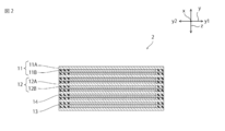
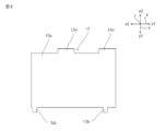
- FIG. 2 is a schematic cross-sectional view of an electric double layer capacitor element in one embodiment of the present invention.
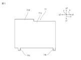
- FIG. 3 is a schematic plan view of a positive electrode in one embodiment of the present invention.
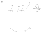
- FIG. 4 is a schematic plan view of a negative electrode in one embodiment of the present invention.
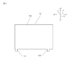
- FIG. 5 is a schematic plan view of the positive electrode in the first modification.
- FIG. 6 is a schematic plan view of the negative electrode in the first modification.
- FIG. 7 is a schematic plan view of the positive electrode in the second modification.
- FIG. 8 is a schematic plan view of the negative electrode in the second modification.
- FIG. 1 is a schematic cross-sectional view of an electric double layer capacitor according to the present embodiment.
- An electric double layer capacitor 1 shown in FIG. 1 includes a first electric double layer capacitor element 1a and a second electric double layer capacitor element 1b enclosed in a package 1c.
- the first and second electric double layer capacitor elements 1a and 1b each have a rectangular shape whose longitudinal direction is parallel to the x-axis direction (first direction).
- the first electric double layer capacitor element 1a and the second electric double layer capacitor element 1b are arranged along the x-axis direction. For this reason, the package 1c also has a rectangular shape whose longitudinal direction is parallel to the x-axis direction.
- the package 1c is provided with a rectangular first cell 1c1 and a rectangular second cell 1c2 adjacent to the first cell 1c1 in the x-axis direction.
- the first electric double layer capacitor element 1a is enclosed in the first cell 1c1.
- a second electric double layer capacitor element 1b is enclosed in the second cell 1c2.
- Each cell 1c1, 1c2 is filled with an electrolytic solution.
- the electrolytic solution includes a cation, an anion, and a solvent.
- the cation preferably used include tetraethylammonium salt.
- the anion preferably used include tetrafluoroborate ion (BF 4 ⁇ ) and bistrifluoromethylsulfonylimide ((CF 3 SO 2 ) 2 N ⁇ ).
- the solvent preferably used include carbonate compounds such as propylene carbonate, ethylene carbonate, diethyl carbonate, and dimethyl carbonate, nitrile compounds, and aqueous solvents such as water.
- the electrolytic solution may be, for example, a crosslinkable gel electrolytic solution or an ionic liquid made of an imidazole compound.
- the first electric double layer capacitor element 1a and the second electric double layer capacitor element 1b are constituted by the same electric double layer capacitor element 2.
- FIG. 2 shows a schematic cross-sectional view of the electric double layer capacitor element 2.
- the electric double layer capacitor element 2 includes a negative electrode 11, a positive electrode 12, a separator 13, and an adhesive layer 14.
- One of the negative electrode 11 and the positive electrode 12 constitutes the first or third electrode, and the other constitutes the second or fourth electrode.
- the negative electrode 11 and the positive electrode 12 are opposed to each other through the separator 13. Specifically, a plurality of negative electrodes 11 and a plurality of positive electrodes 12 are alternately stacked via separators 13.
- the negative electrode 11 includes a negative electrode-side collector electrode 11A.
- the negative electrode side collecting electrode 11A can be made of, for example, an aluminum foil.
- the thickness of 11 A of negative electrode side collector electrodes can be about 10 micrometers or more and 30 micrometers or less, for example.
- a negative electrode side polarizable electrode 11B is provided on the negative electrode side collecting electrode 11A.
- the negative electrode side polarizable electrode 11B is provided only on the main surface facing the positive electrode 12 out of the main surface of the negative electrode side collector electrode 11A.
- the thickness of the negative electrode side polarizable electrode 11B can be, for example, about 10 ⁇ m to 30 ⁇ m.
- the negative electrode side polarizable electrode 11B can be made of, for example, carbon.
- the negative electrode 11 has a rectangular negative electrode body 11a.
- the negative electrode main body 11 a faces the positive electrode 12 with the separator 13 interposed therebetween.
- a rectangular extending portion that extends toward the y1 side from the corner on the y1 side in the x-axis direction (first direction) of the negative electrode body 11a and in the y-axis direction (second direction). 11b is connected.
- a rectangular extending portion 11c extending toward the y1 side is connected to a corner portion on the x2 side in the x-axis direction of the negative electrode body 11a and on the y1 side in the y-axis direction.
- the positive electrode 12 shown in FIGS. 2 and 4 includes a positive electrode-side collector electrode 12A.
- the positive electrode side collector electrode 12A can be made of, for example, an aluminum foil or the like.
- the thickness of the positive electrode side collector electrode 12A can be, for example, about 10 ⁇ m to 30 ⁇ m.
- the positive electrode side polarizable electrode 12B is provided on the positive electrode side collecting electrode 12A. Specifically, the positive electrode side polarizable electrode 12B is provided only on the main surface facing the negative electrode 11 in the main surface of the positive electrode side collecting electrode 12A.
- the thickness of the positive electrode side polarizable electrode 12B can be, for example, about 10 ⁇ m to 30 ⁇ m.
- the positive electrode side polarizable electrode 12B can be made of, for example, carbon.
- the positive electrode 12 has a rectangular positive electrode body 12a.
- the positive electrode main body 12 a faces the negative electrode 11 with the separator 13 interposed therebetween.
- a rectangular extending portion 12b extending toward the y1 side is connected to the x1 side in the x-axis direction of the positive electrode body 12a and from a corner portion on the y1 side in the y-axis direction.
- a rectangular extending portion 12c extending toward the y1 side is connected from the corner portion on the x2 side in the x-axis direction of the positive electrode body 12a and on the y1 side in the y-axis direction.
- the negative electrode 11 and the positive electrode 12 which are adjacent in the z-axis direction (thickness direction) are bonded by an adhesive layer 14.
- the separator 13 is provided between the adjacent negative electrode 11 and positive electrode 12.
- the separator 13 has a larger plate shape than the negative electrode 11 and the positive electrode 12.
- the negative electrode 11 and the positive electrode 12 are isolated by the separator 13.
- Separator 13 can be constituted by a porous sheet having a plurality of open cells, for example.
- the separator 13 is impregnated with an electrolytic solution.
- the first and second cells 1c1 and 1c2 have corner portions 1C1 to 1C4, respectively.
- the first corner 1C1 is located on the x1 side in the x-axis direction and on the y1 side in the y-axis direction.
- the second corner portion 1C2 is located on the x2 side in the x-axis direction and on the y1 side in the y-axis direction.
- the third corner 1C3 is located on the x1 side in the x-axis direction and on the y-axis direction y2 side.
- the fourth corner 1C4 is x2 in the x-axis direction and is located on the y2 side in the y-axis direction.
- the extended portion 11b of the negative electrode 11 and the extended portion 12b of the positive electrode 12 are located at the first corner 1C1.
- the extending portion 12b is located on the outer side (x2 side) in the x-axis direction than the extending portion 11b.
- the extending portion 11c of the negative electrode 11 and the extending portion 12c of the positive electrode 12 are located at the second corner 1C2.
- the extending portion 11c is located on the inner side (x1 side) in the x-axis direction than the extending portion 12c.
- the extended portion 11c of the negative electrode 11 and the extended portion 12c of the positive electrode 12 are located at the second corner 1C2.
- the extending portion 11c is located on the outer side (x1 side) in the x-axis direction than the extending portion 12c.
- the extending portion 11b of the negative electrode 11 and the extending portion 12b of the positive electrode 12 are located at the first corner 1C1.
- the extending portion 12b is located on the inner side (x2 side) in the x-axis direction than the extending portion 11b.
- the negative electrode terminal 15 of the first electric double layer capacitor element 1a is connected to the extending portion 11b of the negative electrode 11 at the first corner 1C1 of the first cell 1c1.
- the negative electrode terminal 15 extends from the extending portion 11b toward the y1 side in the y-axis direction.
- the negative electrode terminal 15 penetrates the sealing portion 1c3 of the package 1c and is drawn to the outside of the first cell 1c1.
- the positive electrode terminal 16 of the first electric double layer capacitor element 1a is connected to the extending portion 12b of the positive electrode 12 at the first corner 1C1 of the first cell 1c1.
- the positive electrode terminal 16 extends from the extending portion 12b toward the y1 side in the y-axis direction.
- the positive electrode terminal 16 penetrates the sealing portion 1c3 of the package 1c and is drawn to the outside of the first cell 1c1.
- the positive electrode terminal 17 of the second electric double layer capacitor element 1b is connected to the extending portion 12c of the positive electrode 12 at the second corner 1C2 of the second cell 1c2.
- the positive terminal 17 extends from the extending portion 12c toward the y1 side in the y-axis direction.
- the positive electrode terminal 17 penetrates the sealing portion 1c3 of the package 1c and is drawn to the outside of the first cell 1c1.
- the positive electrode terminal 17 and the negative electrode terminal 15 are electrically connected by a connecting material 19.
- the negative electrode terminal 18 of the second electric double layer capacitor element 1b extends from the extending portion 11c of the negative electrode 11 toward the y1 side in the y-axis direction at the second corner 1C2 of the second cell 1c2.
- the negative electrode terminal 18 passes through the sealing portion 1c3 of the package 1c and is drawn to the outside of the first cell 1c1.
- the negative electrode terminal 15 drawn out from the package 1c in the first corner 1C1 of the first cell 1c1 adjacent to the first corner 1C1 of the first cell 1c1.
- the positive electrode terminal 17 drawn out from the package 1c at the second corner 1C2 of the second cell 1c2 adjacent to the second cell 1c2.
- the connecting material 19 for connecting the negative electrode terminal 15 and the positive electrode terminal 17 can be shortened. Therefore, the equivalent series resistance of the electric double layer capacitor 1 can be lowered.
- the negative electrode terminal 15 and the positive electrode terminal 16 are provided close to each other at the first corner 1C1 of the first cell 1c1. For this reason, the magnetic field generated around the negative electrode terminal 15 and the magnetic field generated around the positive electrode terminal 16 cancel each other.
- the positive electrode terminal 17 and the negative electrode terminal 18 are provided close to each other at the second corner 1C2 of the second cell 1c2. For this reason, the magnetic field generated around the negative electrode terminal 18 and the magnetic field generated around the positive electrode terminal 17 cancel each other. Further, since the negative electrode terminal 15 and the positive electrode terminal 17 are adjacent to each other, the magnetic field generated around the negative electrode terminal 15 and the magnetic field generated around the positive electrode terminal 17 cancel each other, and the equivalent series inductance can be reduced. Therefore, in the electric double layer capacitor 1, an increase in impedance in the high frequency region is effectively suppressed.
- the electric double layer capacitor 1 extending portions 11b, 11c, 12b, and 12c are provided on the y1 side of the negative electrode main body 11a and the positive electrode main body 12a. For this reason, in each of the first and second cells 1c1 and 1c2, an electrolyte pool is formed on the y1 side of the negative electrode body 11a and the positive electrode body 12a. For this reason, even if the electrolytic solution evaporates or leaks from the cells 1c1 and 1c2, the electrolytic solution between the negative electrode 11 and the positive electrode 12 is unlikely to be insufficient. Therefore, the electric double layer capacitor 1 has a long life.
- the extending portions 11b and 12b are provided in the first corner 1C1, while the extending portions 11c and 12c are provided in the second corner 1C2. For this reason, the displacement of the electric double layer capacitor elements 1a and 1b in the cells 1c1 and 1c2 can be suppressed. Accordingly, the stress applied to the extending portions 11b, 11c, 12b, and 12c and the terminals 15 to 18 can be reduced. Therefore, the extending portions 11b, 11c, 12b, and 12c and the terminals 15 to 18 are not easily broken. In addition, since a gap is hardly generated in the seal portion 1c3 of the package 1c, evaporation and leakage of the electrolytic solution can be effectively suppressed.
- the width of the sealing part along the y1 side edge in the y-axis direction of the package 1c is L1, and the sealing located between the first cell 1c1 and the second cell 1c2
- L1> L2 is satisfied.
- the facing area between the first internal electrode and the second internal electrode can be increased, and both realization of a large capacity and low resistance and a long life can be achieved.
- L1 is increased, the evaporation rate of the electrolytic solution is slowed, so that the life of the electric double layer capacitor can be extended.
- L2 does not affect the evaporation of the electrolytic solution. Therefore, a large electrode area can be secured by making L2 as small as possible.
- FIG. 5 is a schematic plan view of the positive electrode in the first modification.
- FIG. 6 is a schematic plan view of the negative electrode in the first modification.
- the negative electrode 11 has an extending portion 11d extending from the x2 side portion in the x-axis direction of the negative electrode body 11a to the y2 side in the y-axis direction.
- the positive electrode 12 has an extending portion 12d extending from the portion on the x1 side in the x-axis direction of the positive electrode body 12a to the y2 side in the y-axis direction. In the present embodiment, these extending portions 11 d and 12 d are bonded to the separator 13.
- FIG. 7 is a schematic plan view of the positive electrode in the second modification.
- FIG. 8 is a schematic plan view of the negative electrode in the second modification.
- the negative electrode 11 has a plurality of extending portions 11d and 11e extending from the negative electrode main body 11a to the y2 side in the y-axis direction.
- the positive electrode 12 has a plurality of extending portions 12d and 12e extending from the positive electrode main body 12a to the y2 side in the y-axis direction.
- these extending portions 11d, 11e, 12d, and 12e are bonded to the separator 13.
- a plurality of extending portions of the negative electrode 11 and extending portions of the positive electrode 12 are alternately provided along the x-axis direction. It is more preferable.
Landscapes
- Engineering & Computer Science (AREA)
- Power Engineering (AREA)
- Microelectronics & Electronic Packaging (AREA)
- Electric Double-Layer Capacitors Or The Like (AREA)
Abstract
低いインピーダンスを有するパッケージ型の電気二重層コンデンサを提供する。 第1の端子15は、第1のセル1c1の第2のセル1c2と隣り合う角部であって、第1の方向に対して垂直な第2の方向の一方側の角部である第1の角部1C1においてパッケージ1cから引き出されている。第2の端子16は、第1の角部1C1の第1の端子15よりも第1の方向における外側の部分においてパッケージ1cから引き出されている。第3の端子17は、第2のセル1c2の第1のセル1c1と隣り合う角部であって、第1の角部1C1と隣り合う第2の角部1C2においてパッケージ1cから引き出されている。第4の端子18は、第2の角部1C2の第3の端子17よりも第1の方向における外側の部分においてパッケージ1cから引き出されている。
Description
本発明は、電気二重層コンデンサに関する。
従来、例えば携帯電話機などの種々の電子機器にコンデンサが広く用いられている。コンデンサとしては、例えば特許文献1に記載のような電気二重層コンデンサ(Electric double-layer capacitor:EDLC)が知られている。電気二重層コンデンサは、二次電池とは異なり、充放電に際して化学反応を伴わないため、長い製品寿命を有するというメリット、大電流で短時間のうちに充放電させることができるというメリットなどを有する。
例えば、特許文献1には、パッケージ型の電気二重層コンデンサが記載されている。特許文献1に記載の電気二重層コンデンサは、パッケージ内に2つのセルが設けられており、各セルに素子が封入されている。各素子は、矩形状であり、短手方向に配列されている。2つの素子から延びる合計4本の端子は、均等に配されている。
特許文献1に記載されているようなパッケージ型の電気二重層コンデンサにおいて、インピーダンスの上昇を抑制したいという要望がある。
本発明の主な目的は、低いインピーダンスを有するパッケージ型の電気二重層コンデンサを提供することにある。
本発明に係る電気二重層コンデンサは、矩形状の第1の電気二重層コンデンサ素子と、矩形状の第2の電気二重層コンデンサ素子と、パッケージと、電解液とを備える。第1の電気二重層コンデンサ素子は、第1及び第2の端子を有する。第2の電気二重層コンデンサ素子は、第1の電気二重層コンデンサ素子に対して第1の方向の一方側に配されている。第2の電気二重層コンデンサ素子は、第3及び第4の端子を有する。パッケージは、矩形状の第1のセルと、矩形状の第2のセルとを有する。第1のセルには、第1の電気二重層コンデンサ素子が封入されている。第2のセルには、第2の電気二重層コンデンサ素子が封入されている。電解液は、第1及び第2のセルのそれぞれに充填されている。第1の端子は、第1のセルの第2のセルと隣り合う角部であって、第1の方向に対して垂直な第2の方向の一方側の角部である第1の角部においてパッケージから引き出されている。第2の端子は、第1の角部の第1の端子よりも第1の方向における外側の部分においてパッケージから引き出されている。第3の端子は、第2のセルの第1のセルと隣り合う角部であって、第1の角部と隣り合う第2の角部においてパッケージから引き出されている。第4の端子は、第2の角部の第3の端子よりも第1の方向における外側の部分においてパッケージから引き出されている。上記構成によれば、第1の端子と第3の端子とを近接させることができるため、等価直列抵抗を低くすることができる。また、各電気二重層コンデンサ素子の負極端子と正極端子とを近接させることができる。このため、負極端子の周囲に生じる磁界と、正極端子に生じる磁界とが打ち消し合う。その結果、本発明に係る電気二重層コンデンサに高周波や交流電力が印加された場合であってもインピーダンスが低い。
本発明に係る電気二重層コンデンサでは、第1の方向が第1及び第2の電気二重層コンデンサ素子の長手方向と平行であってもよい。
本発明に係る電気二重層コンデンサでは、第1の電気二重層コンデンサ素子は、互いに対向する第1及び第2の電極を有し、第1及び第2の電極は、それぞれ、矩形状の第1の電極本体と、第1の角部に位置しており、第1の電極本体から第2の方向の一方側に向かって延びており、第1または第2の端子に接続されている第1の延設部と、第1のセルの第1の方向における他方側であって第2の方向における一方側に位置している第3の角部に位置しており、第1の電極本体から第2の方向の一方側に向かって延びる第2の延設部とを含み、第2の電気二重層コンデンサ素子は、互いに対向する第3及び第4の電極を有し、第3及び第4の電極は、それぞれ、矩形状の第2の電極本体と、第2の角部に位置しており、第2の電極本体から第2の方向の一方側に向かって延びており、第3または第4の端子に接続されている第3の延設部と、第2のセルの第1の方向における一方側であって第2の方向における一方側に位置している第4の角部に位置しており、第2の電極本体から第2の方向の一方側に向かって延びる第4の延設部とを含んでいることが好ましい。この構成によれば、延設部が設けられている部分に電解液溜まりが形成されるため、経時変化に伴い、正極と負極との間の電解液が蒸発した場合でも、電解液溜まり部分から、正極と負極との間に電解液が供給されるため、正極と負極との間の電解液が不足しにくくなる。
本発明に係る電気二重層コンデンサでは、パッケージの第2の方向の一方側端辺に沿った封止部の幅をL1とし、パッケージの第1のセルと第2のセルとの間に位置する封止部の幅をL2としたときに、L1>L2が満たされることが好ましい。この場合、第1の内部電極と第2の内部電極との対向面積を大きくでき、大容量、低抵抗の実現と長寿命を両立することができる。具体的には、L1を大きくすると電解液の蒸発速度が遅くなるので、電気二重層コンデンサの寿命を延ばすことができる。これに対し、L2は電解液の蒸発に影響しない。したがって、L2は極力小さくすることで、広い電極面積を確保できる。
本発明によれば、低いインピーダンスを有するパッケージ型の電気二重層コンデンサを提供することができる。
以下、本発明を実施した好ましい形態の一例について説明する。但し、下記の実施形態は、単なる例示である。本発明は、下記の実施形態に何ら限定されない。
また、実施形態等において参照する各図面において、実質的に同一の機能を有する部材は同一の符号で参照することとする。また、実施形態等において参照する図面は、模式的に記載されたものである。図面に描画された物体の寸法の比率などは、現実の物体の寸法の比率などとは異なる場合がある。図面相互間においても、物体の寸法比率等が異なる場合がある。具体的な物体の寸法比率等は、以下の説明を参酌して判断されるべきである。
図1は、本実施形態に係る電気二重層コンデンサの模式的断面図である。
図1に示す電気二重層コンデンサ1は、パッケージ1cに封入された第1の電気二重層コンデンサ素子1aと、第2の電気二重層コンデンサ素子1bとを備えている。第1及び第2の電気二重層コンデンサ素子1a、1bは、それぞれ、長手方向がx軸方向(第1の方向)と平行な矩形状である。第1の電気二重層コンデンサ素子1aと、第2の電気二重層コンデンサ素子1bとは、x軸方向に沿って配されている。このため、パッケージ1cも、長手方向がx軸方向と平行な矩形状である。
パッケージ1cには、矩形状の第1のセル1c1と、x軸方向において第1のセル1c1と隣り合う矩形状の第2のセル1c2とが設けられている。第1のセル1c1に第1の電気二重層コンデンサ素子1aが封入されている。第2のセル1c2に第2の電気二重層コンデンサ素子1bが封入されている。
各セル1c1,1c2には、電解液が充填されている。電解液は、陽イオンと、陰イオンと、溶媒とを含む。好ましく用いられる陽イオンとしては、例えば、テトラエチルアンモニウム塩などが挙げられる。好ましく用いられる陰イオンとしては、例えば、四フッ化ホウ酸イオン(BF4
-)や、ビストリフルオロメチルスルホニルイミド((CF3SO2)2N-)などが挙げられる。好ましく用いられる溶媒としては、プロピレンカーボネート、エチレンカーボネート、ジエチルカーボネート、ジメチルカーボネートなどのカーボネート化合物、ニトリル化合物、水などの水系溶媒などが挙げられる。
電解液は、例えば、架橋性のゲル電解液やイミダゾール化合物からなるイオン液体であってもよい。
本実施形態では、第1の電気二重層コンデンサ素子1aと、第2の電気二重層コンデンサ素子1bとは、同様の電気二重層コンデンサ素子2により構成されている。図2に電気二重層コンデンサ素子2の模式的断面図を示す。
図2に示すように、電気二重層コンデンサ素子2は、負極11と、正極12と、セパレータ13と、接着層14とを有する。負極11と正極12とのうちの一方が、第1又は第3の電極を構成しており、他方が第2又は第4の電極を構成している。
負極11と正極12とは、セパレータ13を介して対向している。具体的には、複数の負極11と複数の正極12とが、セパレータ13を介して交互に積層されている。
負極11は、負極側集電極11Aを備えている。負極側集電極11Aは、例えば、アルミニウム箔等により構成することができる。負極側集電極11Aの厚みは、例えば、10μm以上30μm以下程度とすることができる。負極側集電極11Aの上には、負極側分極性電極11Bが設けられている。詳細には、負極側集電極11Aの主面のうち、正極12と対向する主面の上にのみ負極側分極性電極11Bが設けられている。負極側分極性電極11Bの厚みは、例えば、10μm以上30μm以下程度とすることができる。負極側分極性電極11Bは、例えば、カーボン等により構成することができる。
図3に示すように、負極11は、矩形状の負極本体11aを有する。この負極本体11aが正極12とセパレータ13を介して対向している。負極本体11aのx軸方向(第1の方向)におけるx1側であって、y軸方向(第2の方向)におけるy1側の角部からは、y1側に向かって延びる矩形状の延設部11bが接続されている。一方、負極本体11aのx軸方向におけるx2側であって、y軸方向におけるy1側の角部からは、y1側に向かって延びる矩形状の延設部11cが接続されている。
図2及び図4に示す正極12は、正極側集電極12Aを備えている。正極側集電極12Aは、例えば、アルミニウム箔等により構成することができる。正極側集電極12Aの厚みは、例えば、10μm以上30μm以下程度とすることができる。
正極側集電極12Aの上には、正極側分極性電極12Bが設けられている。詳細には、正極側集電極12Aの主面のうち、負極11と対向する主面の上にのみ正極側分極性電極12Bが設けられている。正極側分極性電極12Bの厚みは、例えば、10μm以上30μm以下程度とすることができる。正極側分極性電極12Bは、例えば、カーボン等により構成することができる。
図4に示すように、正極12は、矩形状の正極本体12aを有する。この正極本体12aが負極11とセパレータ13を介して対向している。正極本体12aのx軸方向のx1側であって、y軸方向のy1側の角部からは、y1側に向かって延びる矩形状の延設部12bが接続されている。一方、正極本体12aのx軸方向におけるx2側であって、y軸方向におけるy1側の角部からはy1側に向かって延びる矩形状の延設部12cが接続されている。
z軸方向(厚み方向)において隣り合う負極11と正極12とは、接着層14により接着されている。
図2に示すように、セパレータ13は、隣り合う負極11及び正極12の間に設けられている。セパレータ13は、負極11及び正極12よりも大きな平板状である。このセパレータ13により負極11と正極12とが隔離されている。セパレータ13は、例えば、複数の連続気泡を有する多孔質シートにより構成することができる。セパレータ13には、電解液が含浸している。
第1及び第2のセル1c1,1c2は、それぞれ、角部1C1~1C4を有する。第1の角部1C1は、x軸方向のx1側であって、y軸方向のy1側に位置している。第2の角部1C2は、x軸方向のx2側であって、y軸方向のy1側に位置している。第3の角部1C3は、x軸方向のx1側であって、y軸方向y2側に位置している。第4の角部1C4は、x軸方向のx2であって、y軸方向のy2側に位置している。
図1に示すように、第1の電気二重層コンデンサ素子1aでは、負極11の延設部11bと、正極12の延設部12bとが第1の角部1C1に位置している。延設部12bは、延設部11bよりもx軸方向の外側(x2側)に位置している。負極11の延設部11cと、正極12の延設部12cとが第2の角部1C2に位置している。延設部11cは、延設部12cよりもx軸方向の内側(x1側)に位置している。
第2の電気二重層コンデンサ素子1bでは、負極11の延設部11cと、正極12の延設部12cとが第2の角部1C2に位置している。延設部11cは、延設部12cよりもx軸方向の外側(x1側)に位置している。負極11の延設部11bと、正極12の延設部12bとが第1の角部1C1に位置している。延設部12bは、延設部11bよりもx軸方向の内側(x2側)に位置している。
第1の電気二重層コンデンサ素子1aの負極端子15は、第1のセル1c1の第1の角部1C1において、負極11の延設部11bに接続されている。負極端子15は、延設部11bからy軸方向のy1側に向かって延びている。負極端子15は、パッケージ1cの封止部1c3を貫通して、第1のセル1c1の外側にまで引き出されている。
第1の電気二重層コンデンサ素子1aの正極端子16は、第1のセル1c1の第1の角部1C1において、正極12の延設部12bに接続されている。正極端子16は、延設部12bからy軸方向のy1側に向かって延びている。正極端子16は、パッケージ1cの封止部1c3を貫通して、第1のセル1c1の外側にまで引き出されている。
第2の電気二重層コンデンサ素子1bの正極端子17は、第2のセル1c2の第2の角部1C2において、正極12の延設部12cに接続されている。正極端子17は、延設部12cからy軸方向のy1側に向かって延びている。正極端子17は、パッケージ1cの封止部1c3を貫通して、第1のセル1c1の外側にまで引き出されている。正極端子17と負極端子15とは、接続材19により電気的に接続されている。
第2の電気二重層コンデンサ素子1bの負極端子18は、第2のセル1c2の第2の角部1C2において、負極11の延設部11cからy軸方向のy1側に向かって延びている。負極端子18は、パッケージ1cの封止部1c3を貫通して、第1のセル1c1の外側にまで引き出されている。
以上説明したように、本実施形態では、隣り合う、第1のセル1c1の第1の角部1C1においてパッケージ1cから引き出された負極端子15と、第1のセル1c1の第1の角部1C1と隣り合う第2のセル1c2の第2の角部1C2においてパッケージ1cから引き出された正極端子17とが電気的に接続されている。このため、負極端子15と正極端子17とを接続するための接続材19を短くすることができる。従って、電気二重層コンデンサ1の等価直列抵抗を低くすることができる。
ところで、電気二重層コンデンサ1に電流が流れると、端子15~18の周囲に磁界が発生し、電気二重層コンデンサ1の等価直列インダクタンスが大きくなる。等価直列インダクタンスが大きい状態で、交流電力を印加すると、高周波域での電気二重層コンデンサのインピーダンスが上昇する。
ここで、電気二重層コンデンサ1では、負極端子15と正極端子16とが、第1のセル1c1の第1の角部1C1において近接して設けられている。このため、負極端子15の周囲に生じた磁界と、正極端子16の周囲に生じた磁界とが打ち消し合う。正極端子17と負極端子18とが、第2のセル1c2の第2の角部1C2において近接して設けられている。このため、負極端子18の周囲に生じた磁界と、正極端子17の周囲に生じた磁界とが打ち消し合う。また、負極端子15と正極端子17とも隣り合っているため、負極端子15の周囲に生じた磁界と、正極端子17の周囲に生じた磁界とも打ち消し合い、等価直列インダクタンスを小さくできる。従って、電気二重層コンデンサ1では、高周波域でのインピーダンスの上昇が効果的に抑制されている。
電気二重層コンデンサ1では、負極本体11a及び正極本体12aのy1側に延設部11b、11c、12b、12cが設けられている。このため、第1及び第2のセル1c1,1c2のそれぞれにおいて、負極本体11a及び正極本体12aのy1側に電解液溜まりが形成される。このため、電解液がセル1c1,1c2から蒸発したり漏洩したとしても、負極11と正極12との間の電解液が不足しにくい。従って、電気二重層コンデンサ1は、長い寿命を有する。
また、延設部11b、12bが第1の角部1C1に設けられている一方、延設部11c、12cが第2の角部1C2に設けられている。このため、セル1c1,1c2内における電気二重層コンデンサ素子1a、1bの変位を抑制することができる。従って、延設部11b、11c、12b、12cや端子15~18にかかる応力を小さくできる。よって、延設部11b、11c、12b、12cや端子15~18が破断しにくい。また、パッケージ1cのシール部1c3に隙間が生じにくいため、電解液の蒸発や漏洩を効果的に抑制することができる。
電気二重層コンデンサ1では、パッケージ1cのy軸方向のy1側の端辺に沿った封止部の幅をL1とし、第1のセル1c1と第2のセル1c2との間に位置する封止部の幅をL2としたときに、L1>L2が満たされる。このため、第1の内部電極と第2の内部電極との対向面積を大きくでき、大容量、低抵抗の実現と長寿命を両立することができる。具体的には、L1を大きくすると電解液の蒸発速度が遅くなるので、電気二重層コンデンサの寿命を延ばすことができる。これに対し、L2は電解液の蒸発に影響しない。したがって、L2は極力小さくすることで、広い電極面積を確保できる。
(第1の変形例)
図5は、第1の変形例における正極の模式的平面図である。図6は、第1の変形例における負極の模式的平面図である。
図5は、第1の変形例における正極の模式的平面図である。図6は、第1の変形例における負極の模式的平面図である。
図5に示すように、負極11は、負極本体11aのx軸方向におけるx2側の部分から、y軸方向のy2側に延びる延設部11dを有する。図6に示すように、正極12は、正極本体12aのx軸方向におけるx1側の部分から、y軸方向のy2側に延びる延設部12dを有する。本実施形態では、これら延設部11d、12dがセパレータ13と接着される。
(第2の変形例)
図7は、第2の変形例における正極の模式的平面図である。図8は、第2の変形例における負極の模式的平面図である。
図7は、第2の変形例における正極の模式的平面図である。図8は、第2の変形例における負極の模式的平面図である。
図7に示すように、負極11は、負極本体11aからy軸方向のy2側に延びる複数の延設部11d、11eを有する。図8に示すように、正極12は、正極本体12aからy軸方向のy2側に延びる複数の延設部12d、12eを有する。本実施形態では、これら延設部11d、11e、12d、12eがセパレータ13と接着される。このように、セパレータ13と接着される延設部を負極11及び正極12のそれぞれに対して複数設けることにより電極やセパレータの剥離や折れ曲がりが発生することを抑制することができる。電極やセパレータの剥離や折れ曲がりが発生することをより効果的に抑制する観点からは、負極11の延設部と、正極12の延設部とを、x軸方向に沿って交互に複数ずつ設けることがより好ましい。
1 電気二重層コンデンサ
1a 第1の電気二重層コンデンサ素子
1b 第2の電気二重層コンデンサ
2 電気二重層コンデンサ素子
1c パッケージ
1c1 第1のセル
1c2 第2のセル
1c3 シール部
1C1 第1の角部
1C2 第2の角部
1C3 第3の角部
1C4 第4の角部
11 負極
11A 負極側集電極
11B 負極側分極性電極
11a 負極本体
11b,11c,11d,11e 延設部
12 正極
12A 正極側集電極
12B 正極側分極性電極
12a 正極本体
12b,12c 延設部
13 セパレータ
14 接着層
15,18 負極端子
16,17 正極端子
19 接続材
1a 第1の電気二重層コンデンサ素子
1b 第2の電気二重層コンデンサ
2 電気二重層コンデンサ素子
1c パッケージ
1c1 第1のセル
1c2 第2のセル
1c3 シール部
1C1 第1の角部
1C2 第2の角部
1C3 第3の角部
1C4 第4の角部
11 負極
11A 負極側集電極
11B 負極側分極性電極
11a 負極本体
11b,11c,11d,11e 延設部
12 正極
12A 正極側集電極
12B 正極側分極性電極
12a 正極本体
12b,12c 延設部
13 セパレータ
14 接着層
15,18 負極端子
16,17 正極端子
19 接続材
Claims (4)
- 第1及び第2の端子を有し、矩形状の第1の電気二重層コンデンサ素子と、
前記第1の電気二重層コンデンサ素子に対して第1の方向の一方側に配されており、第3及び第4の端子を有する矩形状の第2の電気二重層コンデンサ素子と、
前記第1の電気二重層コンデンサ素子が封入された矩形状の第1のセルと、前記第2の電気二重層コンデンサ素子が封入された矩形状の第2のセルとを有するパッケージと、 前記第1及び第2のセルのそれぞれに充填された電解液と、
を備え、
前記第1の端子は、前記第1のセルの前記第2のセルと隣り合う角部であって、前記第1の方向に対して垂直な第2の方向の一方側の角部である第1の角部において前記パッケージから引き出されており、
前記第2の端子は、前記第1の角部の前記第1の端子よりも前記第1の方向における外側の部分において前記パッケージから引き出されており、
前記第3の端子は、前記第2のセルの前記第1のセルと隣り合う角部であって、前記第1の角部と隣り合う第2の角部において前記パッケージから引き出されており、
前記第4の端子は、前記第2の角部の前記第3の端子よりも前記第1の方向における外側の部分において前記パッケージから引き出されている、電気二重層コンデンサ。 - 前記第1の方向が前記第1及び第2の電気二重層コンデンサ素子の長手方向と平行である、請求項1に記載の電気二重層コンデンサ。
- 前記第1の電気二重層コンデンサ素子は、互いに対向する第1及び第2の電極を有し、 前記第1及び第2の電極は、それぞれ、
矩形状の第1の電極本体と、
前記第1の角部に位置しており、前記第1の電極本体から前記第2の方向の一方側に向かって延びており、前記第1または第2の端子に接続されている第1の延設部と、
前記第1のセルの前記第1の方向における他方側であって前記第2の方向における一方側に位置している第3の角部に位置しており、前記第1の電極本体から前記第2の方向の一方側に向かって延びる第2の延設部と、
を含み、
前記第2の電気二重層コンデンサ素子は、互いに対向する第3及び第4の電極を有し、 前記第3及び第4の電極は、それぞれ、
矩形状の第2の電極本体と、
前記第2の角部に位置しており、前記第2の電極本体から前記第2の方向の一方側に向かって延びており、前記第3または第4の端子に接続されている第3の延設部と、
前記第2のセルの前記第1の方向における一方側であって前記第2の方向における一方側に位置している第4の角部に位置しており、前記第2の電極本体から前記第2の方向の一方側に向かって延びる第4の延設部と、
を含む、請求項1又は2に記載の電気二重層コンデンサ。 - 前記パッケージの前記第2の方向の一方側端辺に沿った封止部の幅をL1とし、
前記パッケージの前記第1のセルと前記第2のセルとの間に位置する封止部の幅をL2としたときに、
L1>L2
が満たされる、請求項1~3のいずれか一項に記載の電気二重層コンデンサ。
Priority Applications (3)
| Application Number | Priority Date | Filing Date | Title |
|---|---|---|---|
| CN201680014730.4A CN107430943B (zh) | 2015-03-24 | 2016-02-09 | 双电层电容器 |
| JP2017507579A JP6493515B2 (ja) | 2015-03-24 | 2016-02-09 | 電気二重層コンデンサ |
| US15/695,341 US10134532B2 (en) | 2015-03-24 | 2017-09-05 | Electric double-layer capacitor |
Applications Claiming Priority (2)
| Application Number | Priority Date | Filing Date | Title |
|---|---|---|---|
| JP2015-061652 | 2015-03-24 | ||
| JP2015061652A JP2017183299A (ja) | 2015-03-24 | 2015-03-24 | 電気二重層コンデンサ |
Related Child Applications (1)
| Application Number | Title | Priority Date | Filing Date |
|---|---|---|---|
| US15/695,341 Continuation US10134532B2 (en) | 2015-03-24 | 2017-09-05 | Electric double-layer capacitor |
Publications (1)
| Publication Number | Publication Date |
|---|---|
| WO2016152292A1 true WO2016152292A1 (ja) | 2016-09-29 |
Family
ID=56978281
Family Applications (1)
| Application Number | Title | Priority Date | Filing Date |
|---|---|---|---|
| PCT/JP2016/053861 Ceased WO2016152292A1 (ja) | 2015-03-24 | 2016-02-09 | 電気二重層コンデンサ |
Country Status (4)
| Country | Link |
|---|---|
| US (1) | US10134532B2 (ja) |
| JP (2) | JP2017183299A (ja) |
| CN (1) | CN107430943B (ja) |
| WO (1) | WO2016152292A1 (ja) |
Cited By (1)
| Publication number | Priority date | Publication date | Assignee | Title |
|---|---|---|---|---|
| JP2019145757A (ja) * | 2018-02-23 | 2019-08-29 | Tdk株式会社 | 電気化学デバイス |
Families Citing this family (5)
| Publication number | Priority date | Publication date | Assignee | Title |
|---|---|---|---|---|
| MY195773A (en) | 2016-05-20 | 2023-02-11 | Kyocera Avx Components Corp | Multi-Cell Ultracapacitor |
| US11830672B2 (en) | 2016-11-23 | 2023-11-28 | KYOCERA AVX Components Corporation | Ultracapacitor for use in a solder reflow process |
| CN117497335A (zh) * | 2018-02-22 | 2024-02-02 | 京瓷Avx元器件公司 | 具有高电压和低等效串联电阻的封装的超级电容器模块 |
| TWI723680B (zh) * | 2019-12-13 | 2021-04-01 | 位速科技股份有限公司 | 蓄電裝置及蓄電裝置組結構 |
| CN215868988U (zh) * | 2021-05-21 | 2022-02-18 | 阳光电源股份有限公司 | 一种电容结构及功率变换器 |
Citations (2)
| Publication number | Priority date | Publication date | Assignee | Title |
|---|---|---|---|---|
| JP2004296520A (ja) * | 2003-03-25 | 2004-10-21 | Tdk Corp | 電気化学キャパシタ |
| JP2011014859A (ja) * | 2009-01-27 | 2011-01-20 | Panasonic Corp | 電気二重層キャパシタ |
Family Cites Families (11)
| Publication number | Priority date | Publication date | Assignee | Title |
|---|---|---|---|---|
| JP3778253B2 (ja) * | 1999-11-30 | 2006-05-24 | エルナー株式会社 | 複合化電気二重層コンデンサ |
| JP2002313314A (ja) * | 2001-04-09 | 2002-10-25 | Ngk Spark Plug Co Ltd | 薄型非水溶媒2次電池 |
| WO2003107366A1 (ja) * | 2002-06-18 | 2003-12-24 | ティーディーケイ株式会社 | 固体電解コンデンサおよびその製造方法 |
| CA2453328A1 (en) * | 2002-12-16 | 2004-06-16 | Wilson Greatbatch Technologies, Inc. | Dual anode capacitor interconnect design |
| US7203056B2 (en) * | 2003-11-07 | 2007-04-10 | Maxwell Technologies, Inc. | Thermal interconnection for capacitor systems |
| JP3764459B2 (ja) * | 2004-01-20 | 2006-04-05 | 日本無線株式会社 | 電気二重層キャパシタ、それを備えた蓄電装置及び電気二重層キャパシタの製造方法 |
| JP2006221938A (ja) * | 2005-02-09 | 2006-08-24 | Toyota Motor Corp | フィルム外装型蓄電装置 |
| JP2009164468A (ja) * | 2008-01-09 | 2009-07-23 | Nissin Electric Co Ltd | 電気二重層コンデンサモジュール |
| CN102667985B (zh) * | 2009-09-30 | 2016-06-01 | 株式会社半导体能源研究所 | 电化学电容器 |
| JP6273665B2 (ja) * | 2012-09-28 | 2018-02-07 | Tdk株式会社 | 電気化学デバイス |
| KR102197996B1 (ko) * | 2014-05-20 | 2021-01-04 | 삼성에스디아이 주식회사 | 이차전지 제조방법 및 이에 따라 제조된 이차전지 |
-
2015
- 2015-03-24 JP JP2015061652A patent/JP2017183299A/ja active Pending
-
2016
- 2016-02-09 CN CN201680014730.4A patent/CN107430943B/zh not_active Expired - Fee Related
- 2016-02-09 WO PCT/JP2016/053861 patent/WO2016152292A1/ja not_active Ceased
- 2016-02-09 JP JP2017507579A patent/JP6493515B2/ja not_active Expired - Fee Related
-
2017
- 2017-09-05 US US15/695,341 patent/US10134532B2/en not_active Expired - Fee Related
Patent Citations (2)
| Publication number | Priority date | Publication date | Assignee | Title |
|---|---|---|---|---|
| JP2004296520A (ja) * | 2003-03-25 | 2004-10-21 | Tdk Corp | 電気化学キャパシタ |
| JP2011014859A (ja) * | 2009-01-27 | 2011-01-20 | Panasonic Corp | 電気二重層キャパシタ |
Cited By (1)
| Publication number | Priority date | Publication date | Assignee | Title |
|---|---|---|---|---|
| JP2019145757A (ja) * | 2018-02-23 | 2019-08-29 | Tdk株式会社 | 電気化学デバイス |
Also Published As
| Publication number | Publication date |
|---|---|
| JP6493515B2 (ja) | 2019-04-03 |
| CN107430943A (zh) | 2017-12-01 |
| JP2017183299A (ja) | 2017-10-05 |
| JPWO2016152292A1 (ja) | 2017-10-19 |
| CN107430943B (zh) | 2019-03-08 |
| US10134532B2 (en) | 2018-11-20 |
| US20170365421A1 (en) | 2017-12-21 |
Similar Documents
| Publication | Publication Date | Title |
|---|---|---|
| JP6493515B2 (ja) | 電気二重層コンデンサ | |
| US20180233300A1 (en) | Electric double-layer capacitor and method for manufacturing the same | |
| JP6019395B2 (ja) | 蓄電デバイス用電極群及び蓄電デバイス | |
| KR101060869B1 (ko) | 전기 이중층 커패시터 패키지 | |
| JP6428910B2 (ja) | 電気二重層コンデンサ | |
| US20180190440A1 (en) | Electric double layer capacitor and manufacturing method therefor | |
| JP2011228552A (ja) | 電気化学デバイス及びその製造方法 | |
| JP5501270B2 (ja) | 塗布型電極群を用いた電池 | |
| JP2010003773A (ja) | 電気二重層キャパシタ | |
| KR101803086B1 (ko) | 전기화학 커패시터 | |
| WO2017094545A1 (ja) | 電気化学デバイス | |
| JP2011176141A (ja) | 電気化学デバイス | |
| JP2011176137A (ja) | 電気化学デバイス | |
| CN109196703B (zh) | 蓄电设备 | |
| KR101357137B1 (ko) | 전극 조립체 및 이를 구비한 전기에너지 저장장치 | |
| JP2014229832A (ja) | 電気化学デバイス用電極、電気化学デバイス及び電気化学デバイス用電極の製造方法 | |
| KR101211667B1 (ko) | 파우치형 슈퍼 커패시터 및 이의 제작 방법 | |
| JP2011176140A (ja) | 電気化学デバイス | |
| JP7219720B2 (ja) | 電気化学的エネルギー貯蔵デバイス | |
| JP2014063788A (ja) | 電気二重層コンデンサ | |
| JP2013168636A (ja) | 電解液およびこの電解液を用いた電解コンデンサ | |
| JP2011176142A (ja) | 電気化学デバイス | |
| JP2011176138A (ja) | 電気化学デバイス | |
| JP2014127611A (ja) | 電気化学デバイス | |
| JP2011175872A (ja) | 電気化学デバイス |
Legal Events
| Date | Code | Title | Description |
|---|---|---|---|
| 121 | Ep: the epo has been informed by wipo that ep was designated in this application |
Ref document number: 16768195 Country of ref document: EP Kind code of ref document: A1 |
|
| ENP | Entry into the national phase |
Ref document number: 2017507579 Country of ref document: JP Kind code of ref document: A |
|
| NENP | Non-entry into the national phase |
Ref country code: DE |
|
| 122 | Ep: pct application non-entry in european phase |
Ref document number: 16768195 Country of ref document: EP Kind code of ref document: A1 |