WO2016151818A1 - 発光装置 - Google Patents
発光装置 Download PDFInfo
- Publication number
- WO2016151818A1 WO2016151818A1 PCT/JP2015/059236 JP2015059236W WO2016151818A1 WO 2016151818 A1 WO2016151818 A1 WO 2016151818A1 JP 2015059236 W JP2015059236 W JP 2015059236W WO 2016151818 A1 WO2016151818 A1 WO 2016151818A1
- Authority
- WO
- WIPO (PCT)
- Prior art keywords
- conductor
- electrode
- light emitting
- layer
- emitting device
- Prior art date
- Legal status (The legal status is an assumption and is not a legal conclusion. Google has not performed a legal analysis and makes no representation as to the accuracy of the status listed.)
- Ceased
Links
Images






Classifications
-
- H—ELECTRICITY
- H05—ELECTRIC TECHNIQUES NOT OTHERWISE PROVIDED FOR
- H05B—ELECTRIC HEATING; ELECTRIC LIGHT SOURCES NOT OTHERWISE PROVIDED FOR; CIRCUIT ARRANGEMENTS FOR ELECTRIC LIGHT SOURCES, IN GENERAL
- H05B33/00—Electroluminescent light sources
- H05B33/12—Light sources with substantially two-dimensional [2D] radiating surfaces
- H05B33/26—Light sources with substantially two-dimensional [2D] radiating surfaces characterised by the composition or arrangement of the conductive material used as an electrode
- H05B33/28—Light sources with substantially two-dimensional [2D] radiating surfaces characterised by the composition or arrangement of the conductive material used as an electrode of translucent electrodes
-
- H—ELECTRICITY
- H04—ELECTRIC COMMUNICATION TECHNIQUE
- H04N—PICTORIAL COMMUNICATION, e.g. TELEVISION
- H04N1/00—Scanning, transmission or reproduction of documents or the like, e.g. facsimile transmission; Details thereof
- H04N1/024—Details of scanning heads ; Means for illuminating the original
- H04N1/028—Details of scanning heads ; Means for illuminating the original for picture information pick-up
- H04N1/02815—Means for illuminating the original, not specific to a particular type of pick-up head
-
- H—ELECTRICITY
- H10—SEMICONDUCTOR DEVICES; ELECTRIC SOLID-STATE DEVICES NOT OTHERWISE PROVIDED FOR
- H10K—ORGANIC ELECTRIC SOLID-STATE DEVICES
- H10K50/00—Organic light-emitting devices
- H10K50/80—Constructional details
- H10K50/805—Electrodes
-
- H—ELECTRICITY
- H10—SEMICONDUCTOR DEVICES; ELECTRIC SOLID-STATE DEVICES NOT OTHERWISE PROVIDED FOR
- H10K—ORGANIC ELECTRIC SOLID-STATE DEVICES
- H10K50/00—Organic light-emitting devices
- H10K50/80—Constructional details
- H10K50/805—Electrodes
- H10K50/81—Anodes
- H10K50/814—Anodes combined with auxiliary electrodes, e.g. ITO layer combined with metal lines
-
- H—ELECTRICITY
- H10—SEMICONDUCTOR DEVICES; ELECTRIC SOLID-STATE DEVICES NOT OTHERWISE PROVIDED FOR
- H10K—ORGANIC ELECTRIC SOLID-STATE DEVICES
- H10K50/00—Organic light-emitting devices
- H10K50/80—Constructional details
- H10K50/805—Electrodes
- H10K50/82—Cathodes
- H10K50/824—Cathodes combined with auxiliary electrodes
-
- H—ELECTRICITY
- H10—SEMICONDUCTOR DEVICES; ELECTRIC SOLID-STATE DEVICES NOT OTHERWISE PROVIDED FOR
- H10K—ORGANIC ELECTRIC SOLID-STATE DEVICES
- H10K59/00—Integrated devices, or assemblies of multiple devices, comprising at least one organic light-emitting element covered by group H10K50/00
- H10K59/80—Constructional details
- H10K59/805—Electrodes
- H10K59/8051—Anodes
- H10K59/80516—Anodes combined with auxiliary electrodes, e.g. ITO layer combined with metal lines
-
- H—ELECTRICITY
- H10—SEMICONDUCTOR DEVICES; ELECTRIC SOLID-STATE DEVICES NOT OTHERWISE PROVIDED FOR
- H10K—ORGANIC ELECTRIC SOLID-STATE DEVICES
- H10K59/00—Integrated devices, or assemblies of multiple devices, comprising at least one organic light-emitting element covered by group H10K50/00
- H10K59/80—Constructional details
- H10K59/805—Electrodes
- H10K59/8052—Cathodes
- H10K59/80522—Cathodes combined with auxiliary electrodes
-
- H—ELECTRICITY
- H10—SEMICONDUCTOR DEVICES; ELECTRIC SOLID-STATE DEVICES NOT OTHERWISE PROVIDED FOR
- H10K—ORGANIC ELECTRIC SOLID-STATE DEVICES
- H10K71/00—Manufacture or treatment specially adapted for the organic devices covered by this subclass
- H10K71/60—Forming conductive regions or layers, e.g. electrodes
- H10K71/611—Forming conductive regions or layers, e.g. electrodes using printing deposition, e.g. ink jet printing
-
- H—ELECTRICITY
- H10—SEMICONDUCTOR DEVICES; ELECTRIC SOLID-STATE DEVICES NOT OTHERWISE PROVIDED FOR
- H10K—ORGANIC ELECTRIC SOLID-STATE DEVICES
- H10K2102/00—Constructional details relating to the organic devices covered by this subclass
- H10K2102/301—Details of OLEDs
- H10K2102/351—Thickness
Definitions
- the present invention relates to a light emitting device.
- a transparent electrode using a translucent conductive material is formed. Since the translucent conductive material generally has high resistance, the resistance of the transparent electrode is high. For this reason, in order to reduce the resistance of the transparent electrode, an auxiliary electrode may be formed on the transparent electrode, as described in Patent Document 1, for example.
- the auxiliary electrode is formed on a transparent electrode and is covered with an insulating film.
- Patent Document 1 describes ink jet printing as one of the auxiliary electrode forming methods.
- An example of a problem to be solved by the present invention is to reduce the resistance of a conductor by increasing the conductor without increasing the width of the conductor included in the light-emitting device.
- the invention according to claim 1 is a substrate; A light emitting unit formed on the substrate and including a first electrode, a second electrode, and an organic layer positioned between the first electrode and the second electrode; A conductor extending in a first direction and at least part of which is in contact with any surface of the first electrode; With The conductor includes conductive particles and has a first portion and a second portion thicker than the first portion; The first part and the second part are light-emitting devices that are aligned in the first direction and connected to each other.
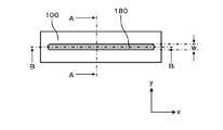
- FIG. 2 is a cross-sectional view taken along the line AA in FIG.
- FIG. 3 is a cross-sectional view taken along the line BB in FIG.
- It is a figure for demonstrating the formation method of a conductor. It is a figure which shows the result after investigating the time from forming a 1st layer to forming a 2nd layer, and the cross-sectional profile of a conductor. It is a top view which shows the structure of the conductor which concerns on 2nd Embodiment.
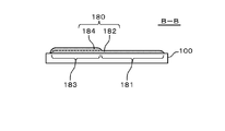
- FIG. 7 is a sectional view taken along line BB in FIG. 1 is a plan view illustrating a configuration of a light emitting device according to Example 1.
- FIG. 6 is a plan view illustrating a configuration of a light emitting device according to Example 2.
- FIG. 13 is a DD cross-sectional view of FIG. 12.
- 6 is a plan view showing a configuration of a light emitting device according to Example 3.
- FIG. 10 is a plan view showing a method for manufacturing the light emitting device according to Example 4;
- FIG. 1 is a plan view of a conductor 180 according to the first embodiment.
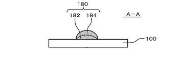
- 2 is a cross-sectional view taken along the line AA in FIG. 1
- FIG. 3 is a cross-sectional view taken along the line BB in FIG.
- the conductor 180 according to the embodiment is formed on the substrate 100 and extends in the first direction (x direction in FIG. 1).
- the conductor 180 has a configuration in which the second layer 184 is overlaid on the first layer 182.
- Each of the first layer 182 and the second layer 184 has conductivity, and is formed by an ink jet method using ink containing conductive particles (for example, nano metal particles such as silver nanoparticles).
- the first layer 182 and the second layer 184 have a configuration in which a plurality of conductive particles are bonded by sintering.
- the heat treatment for sintering the plurality of conductive particles is performed after the first layer 182 and the second layer 184 are formed. For this reason, the boundary between the first layer 182 and the second layer 184 may not exist.
- the conductor 180 has two layers of a first layer 182 and a second layer 184.
- the conductor 180 is formed by repeatedly applying ink containing conductive particles.
- the conductor 180 can be made high without increasing the width of the conductor 180 (for example, 1.9). 2 times to 2.1 times).
- the width w of the conductor 180 is, for example, 100 ⁇ m or less, and the ratio of the height to the width of the conductor 180 (aspect ratio) is, for example, 0.002 (0.1 / 50) times or more.
- the conductor 180 may have a structure in which more layers are stacked (a structure in which multiple layers are applied). In this case, the conductor 180 can be further increased, and the above aspect ratio can be further increased.
- the first layer 182 and the second layer 184 of the conductor 180 are formed using an inkjet method. For this reason, as shown in FIGS. 2 and 3, the end portion of the conductor 180 is gradually thinned away from the center of the conductor 180.
- the conductor 180 is, for example, an auxiliary electrode of a transparent electrode of the light emitting device, but is not limited thereto. Further, another layer (for example, a transparent conductive layer) may be formed between the substrate 100 and the conductor 180.
- FIG. 4 is a diagram for explaining a method of forming the conductor 180.
- the process shown in this figure is performed in the atmosphere, for example.
- the substrate 100 is at room temperature (20 ° C.), for example.
- a first layer 182 is formed.
- the inkjet ejection head 200 has a plurality of ejection nozzles 202.
- droplets are ejected from some of the ejection nozzles 202 (for example, one ejection nozzle 202). It is preferable to discharge.
- the ejection head 200 is moved in the direction opposite to the first direction, and the ejection head 200 is returned to the predetermined position described above. Then, after a predetermined time has elapsed, ink droplets are ejected from the ejection nozzle 202 while moving the ejection head 200 in the first direction again. Thereby, the second layer 184 is formed on the first layer 182.
- the second layer 184 is formed after a predetermined time has elapsed since the first layer 182 was formed.
- the first layer 182 is dried to some extent before the second layer 184 is formed. Therefore, even if the second layer 184 is formed before the first layer 182 is sintered, the second layer 184 is stacked on the first layer 182.
- the height of the conductor 180 is increased by repainting the ink, and the conductor 180 does not spread during the repainting.
- corrugation of the surface of the 2nd layer 184 will become large too much.
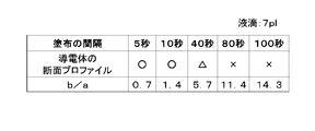
- the degree of drying after ink is ejected from the ejection nozzle 202 until it adheres to the substrate 100 varies depending on the size of the droplet. For this reason, it is preferable to lengthen the said predetermined time as a droplet becomes large. Specifically, when the amount of droplets when forming the first layer 182 is a (picoliter: pl) and the predetermined time is b (seconds), 0.5 ⁇ b / a ⁇ 3 Preferably there is. If it does in this way, the dry state of the 1st layer 182 before the 2nd layer 184 is formed can be made into an appropriate state, for example, the state where the end of the 1st layer 182 was dried.
- the discharge nozzle 202 used when forming the second layer 184 is different from the discharge nozzle 202 used when forming the first layer 182, the first layer 182 and the second layer 184 are different. There is a high possibility that the position is shifted by about several tens of ⁇ m in the y direction in FIG. This is because it is necessary to move the ejection head 200 in the y direction in FIG. 4 to perform alignment, and there is a limit to the accuracy of this alignment. Therefore, in the present embodiment, the same discharge nozzle 202 used when forming the first layer 182 is used as the discharge nozzle 202 used when forming the second layer 184. This eliminates the need to move the ejection head 200 in the y direction between the formation of the first layer 182 and the formation of the second layer 184. Therefore, the second layer 184 can be overlaid on the first layer 182 with high accuracy.
- the substrate 100 is heated.
- the plurality of conductive particles included in the first layer 182 and the plurality of conductive particles included in the second layer 184 are sintered to become the conductor 180.
- at least a part of the shape of the conductive particles remains in the conductor 180.
- the substrate 100 may be heated after forming the first layer 182 and before forming the second layer 184 in order to accelerate the drying of the first layer 182.
- the heating conditions (heating temperature and heating time) at this time are such that the conductive particles of the first layer 182 are not sintered. In this way, the formation time of the conductor 180 can be shortened.
- FIG. 5 shows the time (the above-mentioned predetermined time) from the formation of the first layer 182 to the formation of the second layer 184 in the case where the conductor 180 is formed using ink containing silver nanoparticles.
- FIG. 5 shows the result of having investigated the quality of the cross-sectional profile of the body 180.
- the conductor 180 is formed at atmospheric pressure, and the temperature of the substrate 100 is 20 ° C.
- the amount of liquid droplets discharged from the discharge nozzle 202 is 7 pl.
- b / a is 0.7 and 1.4
- the cross-sectional profile of the conductor 180 is good.
- b / a exceeds 5
- the cross-sectional profile of the conductor 180 deteriorates. From this, it can be said that 0.5 ⁇ b / a ⁇ 3 is preferable.
- the conductor 180 is formed by baking after applying ink repeatedly using the inkjet method. For this reason, the conductor 180 can be made high without increasing the width of the conductor 180. Therefore, the resistance of the conductor 180 can be reduced without increasing the width of the conductor 180.
- the second layer 184 of the conductor 180 is formed after the first layer 182 of the conductor 180 is dried to some extent, the width of the conductor 180 is not widened and the unevenness of the upper surface of the conductor 180 is small. .
- the width of the second layer 184 that is, the width of the conductor 180.
- the width of the conductor 180 does not increase.
- FIG. 6 is a plan view showing the configuration of the conductor 180 according to the second embodiment.
- 7 is a cross-sectional view taken along the line BB of FIG.
- the conductor 180 according to the present embodiment has the same configuration as that of the conductor 180 according to the first embodiment except that the conductor 180 includes the first portion 181 and the second portion 183.
- the first portion 181 is formed only by the first layer 182.
- the second portion 183 is formed by stacking the second layer 184 and the first layer 182. For this reason, the second portion 183 is thicker than the first portion 181. In order to do this, the second layer 184 may be formed only in a portion that becomes the second portion 183.
- the first portion 181 is formed by applying the conductive ink once, and the second portion 183 is formed by applying the conductive ink twice.
- the thickness of the second portion 183 is 180% or more and 220% or less of the thickness of the first portion 181.
- the second portion 183 may be further coated with conductive ink.
- the thickness of the second portion 183 is 90% to 110% of n times the thickness of the first portion 181 (where n is a positive number and 3 or more).
- the width of the first portion 181 is 90% or more and 120% or less of the width of the second portion 183.
- the length of the first portion 181 and the length of the first layer 182 are both 50 ⁇ m or more.
- the thickness of the first portion 181 and the thickness of the second portion 183 are both substantially constant except for the end portions. Further, at the boundary between the first portion 181 and the second portion 183, the thickness of the conductor 180 changes gently.
- the resistance of the conductor 180 can be lowered without increasing the width of the conductor 180.
- the width of the conductor 180 does not increase, and the unevenness of the upper surface of the conductor 180 is small. Then, only part of the conductor 180 can be thickened.
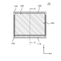
- FIG. 8 is a plan view illustrating the configuration of the light emitting device 10 according to the first embodiment.
- FIG. 9 is a diagram in which the second electrode 130 is removed from FIG.
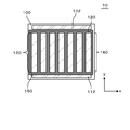
- FIG. 10 is a diagram in which the insulating layer 150 and the organic layer 120 are removed from FIG.
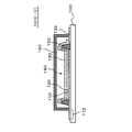
- FIG. 11 is a sectional view taken along the line CC of FIG.
- the sealing part 160 is abbreviate
- the light emitting device 10 includes a substrate 100, a light emitting unit 140, and a conductor 180.
- the light emitting unit 140 is formed on the substrate 100 and includes a first electrode 110, a second electrode 130, and an organic layer 120.
- the organic layer 120 is located between the first electrode 110 and the second electrode 130.
- the conductor 180 is an auxiliary electrode of the first electrode 110 and is in contact with any surface of the first electrode 110. In the example shown in this figure, the conductor 180 is formed on the surface of the first electrode 110 that faces the organic layer 120.
- the conductor 180 has the same configuration as that of the first embodiment.
- the light emitting device 10 will be described in detail.
- the substrate 100 is formed of a light-transmitting material such as glass or a light-transmitting resin.
- the substrate 100 may be formed of a material that does not have translucency.
- the substrate 100 is, for example, a polygon such as a rectangle.
- the substrate 100 may have flexibility.
- the thickness of the substrate 100 is, for example, not less than 10 ⁇ m and not more than 1000 ⁇ m.
- the thickness of the substrate 100 is, for example, 200 ⁇ m or less.
- the material of the substrate 100 includes, for example, PEN (polyethylene naphthalate), PES (polyethersulfone), PET (polyethylene terephthalate), or polyimide. Is formed.
- an inorganic barrier film such as SiN x or SiON is formed on at least the light emitting surface (preferably both surfaces) of the substrate 100 in order to suppress moisture from passing through the substrate 100. ing.
- a light emitting unit 140 is formed on the substrate 100.
- the light emitting unit 140 has a structure for generating light emission, for example, an organic EL element.
- This organic EL element has a configuration in which a first electrode 110, an organic layer 120, and a second electrode 130 are laminated in this order.
- the first electrode 110 is a transparent electrode having optical transparency.
- the transparent conductive material constituting the transparent electrode is a metal-containing material, for example, a metal oxide such as ITO (Indium Tin Oxide), IZO (Indium Zinc Oxide), IWZO (Indium Tungsten Zinc Oxide), ZnO (Zinc Oxide), and the like. is there.
- the thickness of the first electrode 110 is, for example, not less than 10 nm and not more than 500 nm.
- the first electrode 110 is formed using, for example, a sputtering method or a vapor deposition method.
- the first electrode 110 may be a carbon nanotube or a conductive organic material such as PEDOT / PSS.
- the second electrode 130 is made of, for example, a metal selected from the first group consisting of Al, Au, Ag, Pt, Mg, Sn, Zn, and In or an alloy of a metal selected from the first group. Contains a metal layer. In this case, the second electrode 130 has a light shielding property.
- the thickness of the second electrode 130 is, for example, not less than 10 nm and not more than 500 nm. However, the second electrode 130 may be formed using the material exemplified as the material of the first electrode 110.
- the second electrode 130 is formed using, for example, a sputtering method or a vapor deposition method.
- the materials of the first electrode 110 and the second electrode 130 described above are used when light is transmitted through the substrate 100, that is, when light emission from the light emitting device 10 is performed through the substrate 100 (that is, bottom emission type). It is an example. In other cases, light may pass through the side opposite to the substrate 100. That is, the light emission from the light emitting device 10 is performed without passing through the substrate 100 (top emission type).
- top emission type two types of laminated structures of a reverse product type and a forward product type can be adopted. In the reverse product type, the material of the first electrode 110 and the material of the second electrode 130 are opposite to those of the bottom emission type.
- the material of the second electrode 130 is used as the material of the first electrode 110, and the material of the first electrode 110 is used as the material of the second electrode 130.
- the material of the first electrode 110 is formed on the material of the second electrode 130 described above, the organic layer 120 is further formed thereon, and the second electrode 130 is further formed thinly thereon.
- the light is extracted from the side opposite to the substrate 100.
- the thin film forming material is, for example, the material exemplified as the material of the second electrode 130 or an MgAg alloy, and the thickness thereof is, for example, 30 nm or less.
- the light emitting device 10 according to the present embodiment may be of any structure of a bottom emission type and the two types of top emission types described above.
- the organic layer 120 has a configuration in which, for example, a hole injection layer, a light emitting layer, and an electron injection layer are stacked in this order.
- a hole transport layer may be formed between the hole injection layer and the light emitting layer.
- an electron transport layer may be formed between the light emitting layer and the electron injection layer.
- the organic layer 120 may be formed by a vapor deposition method.
- at least one layer of the organic layer 120, for example, a layer in contact with the first electrode may be formed by a coating method such as an inkjet method, a printing method, or a spray method. In this case, the remaining layers of the organic layer 120 are formed by vapor deposition.
- all the layers of the organic layer 120 may be formed using the apply
- the light emitting device 10 has a first terminal 112 and a second terminal 132.
- the first terminal 112 is connected to the first electrode 110
- the second terminal 132 is connected to the second electrode 130.
- the first terminal 112 and the second terminal 132 include a layer formed of the same material as that of the first electrode 110.
- a lead wiring may be provided between the first terminal 112 and the first electrode 110.
- a lead wiring may be provided between the second terminal 132 and the second electrode 130.
- a conductor 180 is formed on the first electrode 110.
- the conductor 180 is an auxiliary electrode for the first electrode 110, and a plurality of conductors 180 are formed on the first electrode 110.
- the conductors 180 extend in the y direction, and a plurality of conductors 180 are arranged at intervals in the x direction.
- the conductor 180 is formed using the method shown in the first embodiment. For this reason, the conductor 180 becomes high, and as a result, the cross-sectional area of the conductor 180 can be increased without increasing the width of the conductor 180. Therefore, the resistance of the conductor 180 can be reduced without expanding the region covered with the conductor 180 (that is, the region where light is not emitted) in the light emitting unit 140.
- the light emitting device 10 has an insulating layer 150.
- the insulating layer 150 is provided on the substrate 100 in order to define the light emitting region of the light emitting unit 140. In the example shown in FIG. 11, the insulating layer 150 covers the edge of the first electrode 110 and the conductor 180.
- the insulating layer 150 is made of, for example, polyimide, epoxy, acrylic, or novolac resin material.
- the insulating layer 150 is formed, for example, by mixing and applying a photosensitive material to a resin material to be the insulating layer 150, and then exposing and developing the resin material.
- the insulating layer 150 may be formed using an inkjet method or a screen printing method.
- the light emitting device 10 has a sealing portion 160.
- the sealing unit 160 seals the light emitting unit 140.
- the sealing portion 160 shown in this figure is a sealing member, and is formed using, for example, a metal such as glass or aluminum, or a resin.
- the sealing portion 160 is a polygon or a circle similar to the substrate 100, and has a shape in which a recess is provided at the center. The edge of the sealing portion 160 is fixed to the substrate 100 with an adhesive. Thereby, the space surrounded by the sealing portion 160 and the substrate 100 is sealed. And the light emission part 140 is located in this sealed space.
- the sealing member may be a film formed by an atomic layer deposition (ALD) method, a chemical vapor deposition (CVD) method, or a film formed by a sputtering method.
- the thickness of the sealing film is, for example, 10 nm or more and 1000 nm or less.
- the sealing film has, for example, at least one of an aluminum oxide film or a titanium oxide film.
- the sealing film is formed using a CVD method or a sputtering method, the sealing film is formed of an insulating film such as SiO 2 or SiN.
- the first electrode 110 is formed on the substrate 100.
- the first terminal 112 and the second terminal 132 are also formed.
- the conductor 180 is formed on the first electrode 110.
- the method for forming the conductor 180 is as described in the first embodiment.
- a resin material to be the insulating layer 150 is applied to the substrate 100, and this resin material is exposed and developed. Thereby, the insulating layer 150 is formed.
- the organic layer 120 is formed in a region surrounded by the first insulating layer 150 in the first electrode 110.
- the second electrode 130 is formed.
- the sealing part 160 is provided.
- the light emitting device 10 has the conductor 180 as the auxiliary electrode of the first electrode 110.
- the conductor 180 is formed by using the method shown in the first embodiment. For this reason, the conductor 180 becomes high. Therefore, the resistance of the conductor 180 can be reduced without expanding the region covered with the conductor 180 (that is, the region where light is not emitted) in the light emitting unit 140.
- FIG. 12 is a plan view illustrating a configuration of the light emitting device 10 according to the second embodiment, and corresponds to FIG. 10 in the first embodiment.
- 13 is a cross-sectional view taken along the line DD of FIG.
- the conductor 180 is also formed on the first terminal 112, and the conductor 180 is also formed on the second terminal 132.
- the configuration is the same as that of the light emitting device 10 according to the first embodiment.
- the conductor 180 on the first terminal 112 is formed continuously with the conductor 180 on the first electrode 110.
- the conductor 180 located on the 1st terminal 112 and the 1st electrode 110 has the structure shown in 2nd Embodiment.
- the conductor 180 on the first electrode 110 is the second portion 183
- the conductor 180 on the first terminal 112 is the first portion 181. Then, in the direction in which the second portion 183 extends, the second portion 183 and the first portion 181 are aligned and connected.
- the conductor 180 on the second terminal 132 is the first portion 181, it has the same thickness as the conductor 180 on the first terminal 112.
- the conductor 180 on the first terminal 112 and the conductor 180 on the second terminal 132 form the first portion 181 because the first terminal 112 and the second terminal 132 need to be translucent. This is because the resistance of the conductor 180 can be reduced by widening the width of the conductor 180.
- the width of the conductor 180 on the first terminal 112 may be the same as the width of the conductor 180 (that is, a portion functioning as an auxiliary electrode) (x direction in FIG. 12).
- the first terminal 112 is connected to a wiring for supplying current from the side surface side of the light emitting device 10. By doing so, the non-light emitting region can be reduced and the aperture ratio of the light emitting device 10 can be increased.
- first portion 181 of the conductor 180 may be provided in a portion that does not overlap with either the first terminal 112 or the second terminal 132.
- the manufacturing method of the light emitting device 10 according to the present embodiment is the same as the manufacturing method of the light emitting device 10 according to the first embodiment.
- the resistance of the conductor 180 can be reduced without expanding the region covered with the conductor 180 in the light emitting unit 140.
- the resistance of the first terminal 112 and the second terminal 132 can be reduced.
- the conductor 180 on the first terminal 112 and the conductor 180 on the second terminal 132 can be made thinner than the conductor 180 on the first electrode 110, The time for forming the conductor 180 on the second terminal 132 can be shortened.
- the first portion 181 is located in the light emitting region, and the second portion 183 is located in the non-light emitting region. In other words, the first portion 181 is on the first terminal 112.
- the second portion 183 is formed on the first electrode 110.
- the layout of the first portion 181 and the second portion 183 is not limited to this.
- the first portion 181 may be formed over the first electrode 110, and the second portion 183 may be formed only on a part of the first electrode 110, preferably near the center of the first electrode 110. This is for suppressing a decrease in luminance caused by an increase in resistance near the center of the light emitting surface of the light emitting device 10.
- the second portion 183 can be spot-formed at the place. Also in this case, since the thickness of the second portion 183 can be made an integral multiple of other portions, the calculation of the current value / resistance value is relatively easy.
- FIG. 14 is a plan view illustrating a configuration of the light emitting device 10 according to the third embodiment, and corresponds to FIG. 12 in the second embodiment.
- the light emitting device 10 according to the present embodiment is related to the second embodiment except that the conductor 180 is formed under the first electrode 110, the first terminal 112, and the second terminal 132.
- the configuration is the same as that of the light emitting device 10.
- the conductor 180 is formed between the first electrode 110 and the substrate 100, between the first terminal 112 and the substrate 100, and between the second terminal 132 and the substrate 100, respectively. .
- the manufacturing method of the light emitting device 10 according to the present example is the light emission according to Example 2, except that the conductor 180 is formed before the first electrode 110, the first terminal 112, and the second terminal 132 are formed. This is the same as the manufacturing method of the device 10.
- the resistance of the conductor 180 can be reduced without expanding the region covered with the conductor 180 in the light emitting unit 140.
- the time for forming the conductor 180 on the first terminal 112 and the second terminal 132 can be shortened.
- FIG. 15 is a plan view illustrating the method for manufacturing the light emitting device 10 according to the fourth embodiment.
- the configuration of the light emitting device 10 is the same as that of any of the first to third embodiments.
- FIG. 15 shows the same case as in the first embodiment.
- the plurality of substrates 100 are connected to each other in the direction in which the conductor 180 extends (first direction: y direction in FIG. 15). Then, when forming the first layer 182 of the conductor 180, the ejection head 200 is moved in the first direction from the standby position. As a result, the first layer 182 of the conductor 180 is formed on each of the plurality of substrates 100.
- the ejection head 200 is moved in the direction opposite to the first direction (the direction of ⁇ y in FIG. 15) without ejecting ink, and returned to the standby position. During this return, the number of substrates 100 is set so that the predetermined time described in the first embodiment elapses.
- the second layer 184 is formed on each of the plurality of substrates 100 by moving the ejection head 200 again in the first direction.
- the plurality of substrates 100 are separated from each other. This separation may be performed after the sealing portion 160 is disposed (or formed) or may be performed before the light emitting device 10 is disposed (or formed).
- the first layer 182 is in a desired dry state while returning the ejection head 200 to the standby position in order to form the second layer 184. For this reason, it is not necessary to make the ejection head 200 stand by anywhere in order to dry the first layer 182. Therefore, the time required for manufacturing the light emitting device 10 is shortened.
- the some 1st electrode 110 is extended in the 1st direction
- the some 2nd electrode 130 is mentioned.
- a display device in which a plurality of light-emitting pixels are provided in a matrix by extending in a second direction orthogonal to the first direction and providing an organic layer at the intersection of the first electrode 110 and the second electrode 130,
- the present invention can be applied.
- a portion overlapping with the terminal may be the first portion 181
- a portion overlapping with the first electrode 110 may be the second portion 183.
- the present invention can employ various configurations other than those described above.
Landscapes
- Engineering & Computer Science (AREA)
- Physics & Mathematics (AREA)
- Optics & Photonics (AREA)
- Multimedia (AREA)
- Signal Processing (AREA)
- Manufacturing & Machinery (AREA)
- Electroluminescent Light Sources (AREA)
Abstract
Description
前記基板に形成され、第1電極、第2電極、及び前記第1電極と前記第2電極の間に位置する有機層を含む発光部と、
第1方向に延在しており、少なくとも一部が前記第1電極のいずれかの面に接している導電体と、
を備え、
前記導電体は、導電粒子を含んでおり、かつ、第1部分と、前記第1部分よりも厚い第2部分とを有し、
前記第1部分と前記第2部分は前記第1方向に並んでおり、かつ繋がっている発光装置である。
図1は、第1の実施形態に係る導電体180の平面図である。図2は図1のA-A断面図であり、図3は図1のB-B断面図である。実施形態に係る導電体180は基板100の上に形成されており、第1の方向(図1におけるx方向)に延在している。導電体180は、第1層182の上に第2層184を重ねた構成を有している。第1層182及び第2層184は、いずれも導電性を有しており、導電粒子(例えば銀ナノ粒子などのナノ金属粒子)を含んだインクを用いて、インクジェット法により形成されている。このため、第1層182及び第2層184は、複数の導電粒子が焼結によって結合した構成を有している。なお、詳細を後述するように、複数の導電粒子を焼結するための熱処理は、第1層182及び第2層184が形成された後に行われている。このため、第1層182と第2層184の境界は存在しない場合もある。
図6は、第2の実施形態に係る導電体180の構成を示す平面図である。図7は図6のB-B断面図である。本実施形態に係る導電体180は、第1部分181及び第2部分183を有している点を除いて、第1の実施形態に係る導電体180と同様の構成である。
図8は、実施例1に係る発光装置10の構成を示す平面図である。図9は、図8から第2電極130を取り除いた図である。図10は、図9から絶縁層150及び有機層120を取り除いた図である。図11は図8のC-C断面図である。なお、説明のため、図8において封止部160は省略されている。
図12は、実施例2に係る発光装置10の構成を示す平面図であり、実施例1における図10に対応している。図13は、図12のD-D断面図である。本実施例に係る発光装置10は、第1端子112の上にも導電体180が形成されており、また、第2端子132の上にも導電体180が形成されている点を除いて、実施例1に係る発光装置10と同様の構成である。
図14は、実施例3に係る発光装置10の構成を示す平面図であり、実施例2における図12に対応している。本実施例に係る発光装置10は、導電体180が第1電極110の下、第1端子112の下、及び第2端子132の下に形成されている点を除いて、実施例2に係る発光装置10と同様の構成である。言い換えると、本実施例において、導電体180は、第1電極110と基板100の間、第1端子112と基板100の間、及び第2端子132と基板100の間のそれぞれに形成されている。
図15は、実施例4に係る発光装置10の製造方法を示す平面図である。本実施例において、発光装置10の構成は実施例1~3のいずれかと同様である。図15は、実施例1と同様の場合を示している。
Claims (8)
- 基板と、
前記基板に形成され、第1電極、第2電極、及び前記第1電極と前記第2電極の間に位置する有機層を含む発光部と、
第1方向に延在しており、少なくとも一部が前記第1電極のいずれかの面に接している導電体と、
を備え、
前記導電体は、導電粒子を含んでおり、かつ、第1部分と、前記第1部分よりも厚い第2部分とを有し、
前記第1部分と前記第2部分は前記第1方向に並んでおり、かつ繋がっている発光装置。 - 請求項1に記載の発光装置において、
前記第1方向に直交する第2方向における断面において、前記第1部分の幅は、前記第2部分の幅の90%以上120%以下である発光装置。 - 請求項1又は2に記載の発光装置において、
前記導電体は、複数の前記導電粒子が結合して形成されている発光装置。 - 請求項1~3のいずれか一項に記載の発光装置において、
前記導電粒子はナノ粒子である発光装置。 - 請求項1~4のいずれか一項に記載の発光装置において、
前記基板に形成され、前記第1電極に電気的に接続する端子を備え、
前記導電体の前記第1部分は前記端子と重なっている発光装置。 - 請求項1~5のいずれか一項に記載の発光装置において、
前記第2部分の厚さは前記第1部分の厚さのn倍(ただしnは正数であり、かつ2以上)の90%以上110%以下である発光装置。 - 請求項6に記載の発光装置において、
前記第2部分は、塗布材料を重ねて塗布することにより形成されている発光装置。 - 請求項1~7のいずれか一項に記載の発光装置において、
複数の前記第1電極が第1の方向に延在し、
複数の前記第2電極が前記第1の方向に直交する第2の方向に延在し、
前記第1電極と前記第2電極の交点のそれぞれに前記有機層が設けられている発光装置。
Priority Applications (3)
| Application Number | Priority Date | Filing Date | Title |
|---|---|---|---|
| PCT/JP2015/059236 WO2016151818A1 (ja) | 2015-03-25 | 2015-03-25 | 発光装置 |
| JP2017507261A JP6657181B2 (ja) | 2015-03-25 | 2015-03-25 | 発光装置 |
| US15/561,322 US10418581B2 (en) | 2015-03-25 | 2015-03-25 | Light emitting device |
Applications Claiming Priority (1)
| Application Number | Priority Date | Filing Date | Title |
|---|---|---|---|
| PCT/JP2015/059236 WO2016151818A1 (ja) | 2015-03-25 | 2015-03-25 | 発光装置 |
Publications (1)
| Publication Number | Publication Date |
|---|---|
| WO2016151818A1 true WO2016151818A1 (ja) | 2016-09-29 |
Family
ID=56977140
Family Applications (1)
| Application Number | Title | Priority Date | Filing Date |
|---|---|---|---|
| PCT/JP2015/059236 Ceased WO2016151818A1 (ja) | 2015-03-25 | 2015-03-25 | 発光装置 |
Country Status (3)
| Country | Link |
|---|---|
| US (1) | US10418581B2 (ja) |
| JP (1) | JP6657181B2 (ja) |
| WO (1) | WO2016151818A1 (ja) |
Cited By (1)
| Publication number | Priority date | Publication date | Assignee | Title |
|---|---|---|---|---|
| JP2020521993A (ja) * | 2017-04-18 | 2020-07-27 | マジック リープ, インコーポレイテッドMagic Leap,Inc. | 反射性流動可能材料によって形成された反射性層を有する導波管 |
Citations (9)
| Publication number | Priority date | Publication date | Assignee | Title |
|---|---|---|---|---|
| JP2000082588A (ja) * | 1997-09-22 | 2000-03-21 | Fuji Electric Co Ltd | 有機発光素子およびその製造方法 |
| JP2003318516A (ja) * | 2002-04-22 | 2003-11-07 | Seiko Epson Corp | 製膜方法及びデバイス及び電子機器並びにデバイスの製造方法 |
| JP2004327070A (ja) * | 2003-04-21 | 2004-11-18 | Seiko Epson Corp | 表示装置及び方法 |
| JP2004335389A (ja) * | 2003-05-12 | 2004-11-25 | Sony Corp | 蒸着マスクおよびこれを用いた表示装置の製造方法、ならびに表示装置 |
| JP2008103305A (ja) * | 2006-10-17 | 2008-05-01 | Lg Electron Inc | 電界発光パネル及びそれを含む光源装置 |
| JP2010234354A (ja) * | 2009-03-09 | 2010-10-21 | Fujifilm Corp | ラインパターン形成方法 |
| JP2011113815A (ja) * | 2009-11-26 | 2011-06-09 | Ricoh Co Ltd | 画像表示装置、画像表示装置の製造方法及び電子機器 |
| WO2011155306A1 (ja) * | 2010-06-07 | 2011-12-15 | Necライティング株式会社 | 有機エレクトロルミネッセンス照明装置 |
| JP2012174517A (ja) * | 2011-02-22 | 2012-09-10 | Panasonic Corp | 有機エレクトロルミネッセンス素子 |
Family Cites Families (12)
| Publication number | Priority date | Publication date | Assignee | Title |
|---|---|---|---|---|
| DE3235724C2 (de) * | 1981-10-02 | 1987-04-23 | Futaba Denshi Kogyo K.K., Mobara, Chiba | Leuchtstoff-Anzeigevorrichtung |
| US4878022A (en) * | 1988-10-14 | 1989-10-31 | The Regents Of The University Of California | Widened and shaped MRI surface coil having increased signal-to-noise ratio |
| CN100578688C (zh) | 2003-10-28 | 2010-01-06 | 住友金属矿山株式会社 | 透明导电层叠体及其制造方法及使用了该层叠体的器件 |
| JP4275644B2 (ja) * | 2004-06-23 | 2009-06-10 | シャープ株式会社 | アクティブマトリクス基板およびその製造方法、並びに電子装置 |
| MX2007016485A (es) * | 2005-06-24 | 2008-03-11 | Universal Supercapacitors Llc | Colector de corriente para capacitores electroquimicos de doble capa electrica y metodo de fabricacion del mismo. |
| CN101297610B (zh) * | 2005-07-29 | 2010-04-21 | 株式会社藤仓 | 弯曲式刚性印刷布线板及其制造方法 |
| US9440003B2 (en) * | 2005-11-04 | 2016-09-13 | Boston Scientific Scimed, Inc. | Medical devices having particle-containing regions with diamond-like coatings |
| JP2008238631A (ja) * | 2007-03-28 | 2008-10-09 | Toppan Forms Co Ltd | 印刷物およびこれを用いた印刷物の真贋判定方法 |
| US8114720B2 (en) | 2008-12-25 | 2012-02-14 | Semiconductor Energy Laboratory Co., Ltd. | Semiconductor device and manufacturing method thereof |
| JP5287262B2 (ja) | 2009-01-07 | 2013-09-11 | セイコーエプソン株式会社 | アクティブマトリクス基板、電気泳動表示装置及び電子機器 |
| US9188323B2 (en) | 2010-10-20 | 2015-11-17 | Semiconductor Energy Laboratory Co., Ltd. | Lighting device |
| JP5421218B2 (ja) | 2010-10-26 | 2014-02-19 | 出光興産株式会社 | 光電変換装置、及び光電変換装置の製造方法 |
-
2015
- 2015-03-25 JP JP2017507261A patent/JP6657181B2/ja not_active Expired - Fee Related
- 2015-03-25 US US15/561,322 patent/US10418581B2/en active Active
- 2015-03-25 WO PCT/JP2015/059236 patent/WO2016151818A1/ja not_active Ceased
Patent Citations (9)
| Publication number | Priority date | Publication date | Assignee | Title |
|---|---|---|---|---|
| JP2000082588A (ja) * | 1997-09-22 | 2000-03-21 | Fuji Electric Co Ltd | 有機発光素子およびその製造方法 |
| JP2003318516A (ja) * | 2002-04-22 | 2003-11-07 | Seiko Epson Corp | 製膜方法及びデバイス及び電子機器並びにデバイスの製造方法 |
| JP2004327070A (ja) * | 2003-04-21 | 2004-11-18 | Seiko Epson Corp | 表示装置及び方法 |
| JP2004335389A (ja) * | 2003-05-12 | 2004-11-25 | Sony Corp | 蒸着マスクおよびこれを用いた表示装置の製造方法、ならびに表示装置 |
| JP2008103305A (ja) * | 2006-10-17 | 2008-05-01 | Lg Electron Inc | 電界発光パネル及びそれを含む光源装置 |
| JP2010234354A (ja) * | 2009-03-09 | 2010-10-21 | Fujifilm Corp | ラインパターン形成方法 |
| JP2011113815A (ja) * | 2009-11-26 | 2011-06-09 | Ricoh Co Ltd | 画像表示装置、画像表示装置の製造方法及び電子機器 |
| WO2011155306A1 (ja) * | 2010-06-07 | 2011-12-15 | Necライティング株式会社 | 有機エレクトロルミネッセンス照明装置 |
| JP2012174517A (ja) * | 2011-02-22 | 2012-09-10 | Panasonic Corp | 有機エレクトロルミネッセンス素子 |
Cited By (1)
| Publication number | Priority date | Publication date | Assignee | Title |
|---|---|---|---|---|
| JP2020521993A (ja) * | 2017-04-18 | 2020-07-27 | マジック リープ, インコーポレイテッドMagic Leap,Inc. | 反射性流動可能材料によって形成された反射性層を有する導波管 |
Also Published As
| Publication number | Publication date |
|---|---|
| US20180102495A1 (en) | 2018-04-12 |
| JP6657181B2 (ja) | 2020-03-04 |
| JPWO2016151818A1 (ja) | 2017-12-28 |
| US10418581B2 (en) | 2019-09-17 |
Similar Documents
| Publication | Publication Date | Title |
|---|---|---|
| CN110246878A (zh) | 有机发光二极管显示装置 | |
| JP5596858B2 (ja) | 有機エレクトロルミネッセンスパネル及びその製造方法 | |
| JP6657181B2 (ja) | 発光装置 | |
| CN105789259B (zh) | 有机电致发光显示面板及其制作方法、显示装置 | |
| US20240163984A1 (en) | Light emitting device | |
| JP2023116822A (ja) | 発光装置 | |
| WO2016151817A1 (ja) | 導電体の形成方法 | |
| JP2022009669A (ja) | 発光装置 | |
| JP2020074328A (ja) | 発光装置 | |
| JP6661373B2 (ja) | 発光装置 | |
| JP6378769B2 (ja) | 光学装置 | |
| JP7102131B2 (ja) | トップエミッション型の有機el素子およびその製造方法 | |
| WO2014162453A1 (ja) | 接合構造および発光装置 | |
| JP6457065B2 (ja) | 発光装置 | |
| WO2017119068A1 (ja) | 発光装置 | |
| JP2016181426A (ja) | 発光装置 | |
| WO2014162934A1 (ja) | 光学装置 | |
| JP6580336B2 (ja) | 発光装置 | |
| JPWO2017163331A1 (ja) | 発光装置、電子装置および発光装置の製造方法 | |
| JP6700013B2 (ja) | 発光装置 | |
| JP6499876B2 (ja) | 発光装置 | |
| WO2017122360A1 (ja) | 発光装置 | |
| JP2019192662A (ja) | 発光装置 | |
| JP2016181425A (ja) | 発光装置の製造方法 | |
| WO2014162451A1 (ja) | 接合構造および発光装置 |
Legal Events
| Date | Code | Title | Description |
|---|---|---|---|
| 121 | Ep: the epo has been informed by wipo that ep was designated in this application |
Ref document number: 15886371 Country of ref document: EP Kind code of ref document: A1 |
|
| ENP | Entry into the national phase |
Ref document number: 2017507261 Country of ref document: JP Kind code of ref document: A |
|
| WWE | Wipo information: entry into national phase |
Ref document number: 15561322 Country of ref document: US |
|
| NENP | Non-entry into the national phase |
Ref country code: DE |
|
| 122 | Ep: pct application non-entry in european phase |
Ref document number: 15886371 Country of ref document: EP Kind code of ref document: A1 |