WO2016143682A1 - 照明装置、表示装置、及びテレビ受信装置 - Google Patents
照明装置、表示装置、及びテレビ受信装置 Download PDFInfo
- Publication number
- WO2016143682A1 WO2016143682A1 PCT/JP2016/056711 JP2016056711W WO2016143682A1 WO 2016143682 A1 WO2016143682 A1 WO 2016143682A1 JP 2016056711 W JP2016056711 W JP 2016056711W WO 2016143682 A1 WO2016143682 A1 WO 2016143682A1
- Authority
- WO
- WIPO (PCT)
- Prior art keywords
- light
- wavelength conversion
- phosphor
- plate
- wavelength
- Prior art date
Links
Images


Classifications
-
- G—PHYSICS
- G02—OPTICS
- G02F—OPTICAL DEVICES OR ARRANGEMENTS FOR THE CONTROL OF LIGHT BY MODIFICATION OF THE OPTICAL PROPERTIES OF THE MEDIA OF THE ELEMENTS INVOLVED THEREIN; NON-LINEAR OPTICS; FREQUENCY-CHANGING OF LIGHT; OPTICAL LOGIC ELEMENTS; OPTICAL ANALOGUE/DIGITAL CONVERTERS
- G02F1/00—Devices or arrangements for the control of the intensity, colour, phase, polarisation or direction of light arriving from an independent light source, e.g. switching, gating or modulating; Non-linear optics
- G02F1/01—Devices or arrangements for the control of the intensity, colour, phase, polarisation or direction of light arriving from an independent light source, e.g. switching, gating or modulating; Non-linear optics for the control of the intensity, phase, polarisation or colour
- G02F1/13—Devices or arrangements for the control of the intensity, colour, phase, polarisation or direction of light arriving from an independent light source, e.g. switching, gating or modulating; Non-linear optics for the control of the intensity, phase, polarisation or colour based on liquid crystals, e.g. single liquid crystal display cells
- G02F1/133—Constructional arrangements; Operation of liquid crystal cells; Circuit arrangements
- G02F1/1333—Constructional arrangements; Manufacturing methods
- G02F1/1335—Structural association of cells with optical devices, e.g. polarisers or reflectors
- G02F1/1336—Illuminating devices
- G02F1/133602—Direct backlight
- G02F1/133606—Direct backlight including a specially adapted diffusing, scattering or light controlling members
-
- F—MECHANICAL ENGINEERING; LIGHTING; HEATING; WEAPONS; BLASTING
- F21—LIGHTING
- F21S—NON-PORTABLE LIGHTING DEVICES; SYSTEMS THEREOF; VEHICLE LIGHTING DEVICES SPECIALLY ADAPTED FOR VEHICLE EXTERIORS
- F21S2/00—Systems of lighting devices, not provided for in main groups F21S4/00 - F21S10/00 or F21S19/00, e.g. of modular construction
-
- F—MECHANICAL ENGINEERING; LIGHTING; HEATING; WEAPONS; BLASTING
- F21—LIGHTING
- F21K—NON-ELECTRIC LIGHT SOURCES USING LUMINESCENCE; LIGHT SOURCES USING ELECTROCHEMILUMINESCENCE; LIGHT SOURCES USING CHARGES OF COMBUSTIBLE MATERIAL; LIGHT SOURCES USING SEMICONDUCTOR DEVICES AS LIGHT-GENERATING ELEMENTS; LIGHT SOURCES NOT OTHERWISE PROVIDED FOR
- F21K9/00—Light sources using semiconductor devices as light-generating elements, e.g. using light-emitting diodes [LED] or lasers
- F21K9/60—Optical arrangements integrated in the light source, e.g. for improving the colour rendering index or the light extraction
- F21K9/61—Optical arrangements integrated in the light source, e.g. for improving the colour rendering index or the light extraction using light guides
-
- F—MECHANICAL ENGINEERING; LIGHTING; HEATING; WEAPONS; BLASTING
- F21—LIGHTING
- F21K—NON-ELECTRIC LIGHT SOURCES USING LUMINESCENCE; LIGHT SOURCES USING ELECTROCHEMILUMINESCENCE; LIGHT SOURCES USING CHARGES OF COMBUSTIBLE MATERIAL; LIGHT SOURCES USING SEMICONDUCTOR DEVICES AS LIGHT-GENERATING ELEMENTS; LIGHT SOURCES NOT OTHERWISE PROVIDED FOR
- F21K9/00—Light sources using semiconductor devices as light-generating elements, e.g. using light-emitting diodes [LED] or lasers
- F21K9/60—Optical arrangements integrated in the light source, e.g. for improving the colour rendering index or the light extraction
- F21K9/64—Optical arrangements integrated in the light source, e.g. for improving the colour rendering index or the light extraction using wavelength conversion means distinct or spaced from the light-generating element, e.g. a remote phosphor layer
-
- G—PHYSICS
- G02—OPTICS
- G02F—OPTICAL DEVICES OR ARRANGEMENTS FOR THE CONTROL OF LIGHT BY MODIFICATION OF THE OPTICAL PROPERTIES OF THE MEDIA OF THE ELEMENTS INVOLVED THEREIN; NON-LINEAR OPTICS; FREQUENCY-CHANGING OF LIGHT; OPTICAL LOGIC ELEMENTS; OPTICAL ANALOGUE/DIGITAL CONVERTERS
- G02F1/00—Devices or arrangements for the control of the intensity, colour, phase, polarisation or direction of light arriving from an independent light source, e.g. switching, gating or modulating; Non-linear optics
- G02F1/01—Devices or arrangements for the control of the intensity, colour, phase, polarisation or direction of light arriving from an independent light source, e.g. switching, gating or modulating; Non-linear optics for the control of the intensity, phase, polarisation or colour
- G02F1/13—Devices or arrangements for the control of the intensity, colour, phase, polarisation or direction of light arriving from an independent light source, e.g. switching, gating or modulating; Non-linear optics for the control of the intensity, phase, polarisation or colour based on liquid crystals, e.g. single liquid crystal display cells
- G02F1/133—Constructional arrangements; Operation of liquid crystal cells; Circuit arrangements
- G02F1/1333—Constructional arrangements; Manufacturing methods
- G02F1/1335—Structural association of cells with optical devices, e.g. polarisers or reflectors
- G02F1/1336—Illuminating devices
- G02F1/133602—Direct backlight
- G02F1/133603—Direct backlight with LEDs
-
- G—PHYSICS
- G02—OPTICS
- G02F—OPTICAL DEVICES OR ARRANGEMENTS FOR THE CONTROL OF LIGHT BY MODIFICATION OF THE OPTICAL PROPERTIES OF THE MEDIA OF THE ELEMENTS INVOLVED THEREIN; NON-LINEAR OPTICS; FREQUENCY-CHANGING OF LIGHT; OPTICAL LOGIC ELEMENTS; OPTICAL ANALOGUE/DIGITAL CONVERTERS
- G02F1/00—Devices or arrangements for the control of the intensity, colour, phase, polarisation or direction of light arriving from an independent light source, e.g. switching, gating or modulating; Non-linear optics
- G02F1/01—Devices or arrangements for the control of the intensity, colour, phase, polarisation or direction of light arriving from an independent light source, e.g. switching, gating or modulating; Non-linear optics for the control of the intensity, phase, polarisation or colour
- G02F1/13—Devices or arrangements for the control of the intensity, colour, phase, polarisation or direction of light arriving from an independent light source, e.g. switching, gating or modulating; Non-linear optics for the control of the intensity, phase, polarisation or colour based on liquid crystals, e.g. single liquid crystal display cells
- G02F1/133—Constructional arrangements; Operation of liquid crystal cells; Circuit arrangements
- G02F1/1333—Constructional arrangements; Manufacturing methods
- G02F1/1335—Structural association of cells with optical devices, e.g. polarisers or reflectors
- G02F1/1336—Illuminating devices
- G02F1/133615—Edge-illuminating devices, i.e. illuminating from the side
-
- F—MECHANICAL ENGINEERING; LIGHTING; HEATING; WEAPONS; BLASTING
- F21—LIGHTING
- F21Y—INDEXING SCHEME ASSOCIATED WITH SUBCLASSES F21K, F21L, F21S and F21V, RELATING TO THE FORM OR THE KIND OF THE LIGHT SOURCES OR OF THE COLOUR OF THE LIGHT EMITTED
- F21Y2115/00—Light-generating elements of semiconductor light sources
- F21Y2115/10—Light-emitting diodes [LED]
-
- G—PHYSICS
- G02—OPTICS
- G02F—OPTICAL DEVICES OR ARRANGEMENTS FOR THE CONTROL OF LIGHT BY MODIFICATION OF THE OPTICAL PROPERTIES OF THE MEDIA OF THE ELEMENTS INVOLVED THEREIN; NON-LINEAR OPTICS; FREQUENCY-CHANGING OF LIGHT; OPTICAL LOGIC ELEMENTS; OPTICAL ANALOGUE/DIGITAL CONVERTERS
- G02F1/00—Devices or arrangements for the control of the intensity, colour, phase, polarisation or direction of light arriving from an independent light source, e.g. switching, gating or modulating; Non-linear optics
- G02F1/01—Devices or arrangements for the control of the intensity, colour, phase, polarisation or direction of light arriving from an independent light source, e.g. switching, gating or modulating; Non-linear optics for the control of the intensity, phase, polarisation or colour
- G02F1/13—Devices or arrangements for the control of the intensity, colour, phase, polarisation or direction of light arriving from an independent light source, e.g. switching, gating or modulating; Non-linear optics for the control of the intensity, phase, polarisation or colour based on liquid crystals, e.g. single liquid crystal display cells
- G02F1/133—Constructional arrangements; Operation of liquid crystal cells; Circuit arrangements
- G02F1/1333—Constructional arrangements; Manufacturing methods
- G02F1/1335—Structural association of cells with optical devices, e.g. polarisers or reflectors
- G02F1/1336—Illuminating devices
- G02F1/133602—Direct backlight
- G02F1/133608—Direct backlight including particular frames or supporting means
-
- G—PHYSICS
- G02—OPTICS
- G02F—OPTICAL DEVICES OR ARRANGEMENTS FOR THE CONTROL OF LIGHT BY MODIFICATION OF THE OPTICAL PROPERTIES OF THE MEDIA OF THE ELEMENTS INVOLVED THEREIN; NON-LINEAR OPTICS; FREQUENCY-CHANGING OF LIGHT; OPTICAL LOGIC ELEMENTS; OPTICAL ANALOGUE/DIGITAL CONVERTERS
- G02F1/00—Devices or arrangements for the control of the intensity, colour, phase, polarisation or direction of light arriving from an independent light source, e.g. switching, gating or modulating; Non-linear optics
- G02F1/01—Devices or arrangements for the control of the intensity, colour, phase, polarisation or direction of light arriving from an independent light source, e.g. switching, gating or modulating; Non-linear optics for the control of the intensity, phase, polarisation or colour
- G02F1/13—Devices or arrangements for the control of the intensity, colour, phase, polarisation or direction of light arriving from an independent light source, e.g. switching, gating or modulating; Non-linear optics for the control of the intensity, phase, polarisation or colour based on liquid crystals, e.g. single liquid crystal display cells
- G02F1/133—Constructional arrangements; Operation of liquid crystal cells; Circuit arrangements
- G02F1/1333—Constructional arrangements; Manufacturing methods
- G02F1/1335—Structural association of cells with optical devices, e.g. polarisers or reflectors
- G02F1/1336—Illuminating devices
- G02F1/133602—Direct backlight
- G02F1/133613—Direct backlight characterized by the sequence of light sources
-
- G—PHYSICS
- G02—OPTICS
- G02F—OPTICAL DEVICES OR ARRANGEMENTS FOR THE CONTROL OF LIGHT BY MODIFICATION OF THE OPTICAL PROPERTIES OF THE MEDIA OF THE ELEMENTS INVOLVED THEREIN; NON-LINEAR OPTICS; FREQUENCY-CHANGING OF LIGHT; OPTICAL LOGIC ELEMENTS; OPTICAL ANALOGUE/DIGITAL CONVERTERS
- G02F1/00—Devices or arrangements for the control of the intensity, colour, phase, polarisation or direction of light arriving from an independent light source, e.g. switching, gating or modulating; Non-linear optics
- G02F1/01—Devices or arrangements for the control of the intensity, colour, phase, polarisation or direction of light arriving from an independent light source, e.g. switching, gating or modulating; Non-linear optics for the control of the intensity, phase, polarisation or colour
- G02F1/13—Devices or arrangements for the control of the intensity, colour, phase, polarisation or direction of light arriving from an independent light source, e.g. switching, gating or modulating; Non-linear optics for the control of the intensity, phase, polarisation or colour based on liquid crystals, e.g. single liquid crystal display cells
- G02F1/133—Constructional arrangements; Operation of liquid crystal cells; Circuit arrangements
- G02F1/1333—Constructional arrangements; Manufacturing methods
- G02F1/1335—Structural association of cells with optical devices, e.g. polarisers or reflectors
- G02F1/1336—Illuminating devices
- G02F1/133614—Illuminating devices using photoluminescence, e.g. phosphors illuminated by UV or blue light
Definitions
- the blue LED element provided in the LED 17 is a semiconductor made of a semiconductor material such as InGaN, for example, and is blue monochromatic light having a wavelength included in a blue wavelength region (about 420 nm to about 500 nm) when a voltage is applied in the forward direction. Is supposed to emit light. That is, the light emitted from the LED 17 is monochromatic light having the same color as the light emitted from the blue LED element.
- This blue LED element is connected to a wiring pattern on the LED substrate 18 arranged outside the case by a lead frame (not shown).
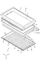
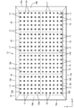
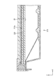
- the LED boards 18 having the above-described configuration are arranged in parallel in the chassis 14 in a state where the long side direction and the short side direction are aligned with each other along the X axis direction and the Y axis direction.
- the LED boards 18 are arranged in the chassis 14 by four pieces (relatively large numbers) along the X-axis direction and by two pieces (relatively small numbers) along the Y-axis direction.
- the arrangement directions thereof coincide with the X-axis direction and the Y-axis direction, respectively.
- the arrangement interval between the LED substrates 18 adjacent to each other in the X-axis direction and the Y-axis direction is substantially constant.
- the reflection sheet 19 is made of a synthetic resin and has a white surface with excellent light reflectivity.
- the reflection sheet 19 does not absorb light of a specific wavelength on the surface thereof, and diffusely reflects all visible rays, and the light reflectance is substantially constant over the entire area.
- the reflection sheet 19 has a size that is laid over almost the entire inner surface of the chassis 14, so that the LED board 18 disposed in the chassis 14 is almost entirely on the front side. It is possible to cover from (light emitting side, optical member 15 side).
- the reflection sheet 19 can reflect the light in the chassis 14 toward the front side (light emission side, optical member 15 side).
- the wavelength conversion efficiency of light in the outer peripheral side portion is lower than the same wavelength conversion efficiency in the central side portion.
- the light transmitted through the side portion has a color similar to that of the light of the LED 17 (primary light), i.e., a blue tint, than the light transmitted through the central side portion. That is, there is a concern that the color unevenness in which the emitted light of the backlight device 12 is close to white on the center side but becomes more bluish on the outer peripheral side is visible.
- the wavelength conversion sheet 20 contains a quantum dot phosphor as a phosphor. If it does in this way, while the wavelength conversion efficiency of the light by the wavelength conversion sheet 20 will become higher, the color purity of the wavelength-converted light will become high.
- the quantum dot phosphor is likely to be deteriorated by moisture absorption or the like compared to other phosphors, and the wavelength conversion efficiency is likely to be lowered at the outer peripheral side portion of the wavelength conversion sheet 20, As described above, the light transmitted through the wavelength conversion sheet 20 is given a diffusing action by the diffusing plate 15a, so that it is difficult for color unevenness to occur to occur.
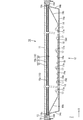
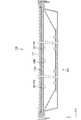
- the alignment direction of the LED 317 (LED substrate 318) and the light guide plate 26 coincides with the Y-axis direction, whereas the alignment direction of the optical member 315 (liquid crystal panel 311) and the light guide plate 26 matches the Z-axis direction. It is assumed that both directions are orthogonal to each other.
- the light guide plate 26 introduces the light emitted from the LED 317 in the Y-axis direction, and rises and emits the light toward the optical member 315 side (Z-axis direction) while propagating the light inside.
- At least one of the light exit surface 26a of the light guide plate 26 and the plate surface 26c on the opposite side thereof is a reflective portion (not shown) that reflects internal light or a scattering portion that scatters internal light (see FIG. (Not shown) is patterned so as to have a predetermined in-plane distribution, so that the emitted light from the light emitting surface 26a is controlled to have a uniform distribution in the surface.
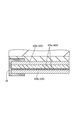
- the wavelength conversion sheet 420 is provided with a sealing portion 29 that seals the outer peripheral edge portion thereof.
- the sealing portion 29 is provided in such a manner that the outer peripheral edge portions of the phosphor layer 420a and the pair of protective layers 420b are collectively sandwiched over the entire circumference, so that the outer peripheral end of the phosphor layer 420a is exposed to the outside. It is supposed to be prevented from being exposed to the outside air. According to such a configuration, it is difficult for the phosphor layer 420a to deteriorate due to moisture contained in the outside air.
Abstract
Description
上記した特許文献1に記載されたようなリモート蛍光体フィルムは、QD蛍光体材料の吸湿などによる劣化を抑制するため、金属酸化膜からなるバリア層を備えている。しかしながら、リモート蛍光体フィルムの外周端は、外気に含まれる水分などに曝され易いものとなっている。このため、リモート蛍光体フィルムのうち外周側部分では、局所的にQD蛍光体材料が吸湿などによって劣化し易くなっており、結果として色ムラが生じるおそれがあった。
本発明の照明装置は、光源と、前記光源からの光を波長変換する蛍光体を含有する波長変換部材と、前記光源からの光に拡散作用を付与する拡散板であって、前記波長変換部材よりも厚く、前記波長変換部材に対して出光側に配される拡散板と、を備える。
(1)前記波長変換部材は、前記拡散板のうち出光側とは反対側の板面に貼り付けられている。このようにすれば、波長変換部材の平坦性を拡散板によって担保することができる。
本発明によれば、色ムラの発生を抑制することができる。
本発明の実施形態1を図1から図8によって説明する。本実施形態では、液晶表示装置10について例示する。なお、各図面の一部にはX軸、Y軸及びZ軸を示しており、各軸方向が各図面で示した方向となるように描かれている。また、図4及び図5などに示す上側を表側とし、同図下側を裏側とする。
本発明の実施形態2を図9から図11によって説明する。この実施形態2では、波長変換シート120の構成を変更したものを示す。なお、上記した実施形態1と同様の構造、作用及び効果について重複する説明は省略する。
本発明の実施形態3を図12によって説明する。この実施形態3では、上記した実施形態1に記載した構成に第2の拡散板25を追加するなどしたものを示す。なお、上記した実施形態1と同様の構造、作用及び効果について重複する説明は省略する。
本発明の実施形態4を図13及び図14によって説明する。この実施形態4では、上記した実施形態1からバックライト装置312をエッジライト型に変更したものを示す。なお、上記した実施形態1と同様の構造、作用及び効果について重複する説明は省略する。
本発明の実施形態5を図15によって説明する。この実施形態5では、上記した実施形態1から波長変換シート420の構成を変更したものを示す。なお、上記した実施形態1と同様の構造、作用及び効果について重複する説明は省略する。
本発明は上記記述及び図面によって説明した実施形態に限定されるものではなく、例えば次のような実施形態も本発明の技術的範囲に含まれる。
(1)上記した各実施形態では、3枚の光学シートを備える構成を例示したが、光学シートの枚数は2枚以下または4枚以上に変更することも可能である。また、波長変換シートを除いて使用する光学シートの種類についても適宜に変更可能であり、例えば拡散シートやマイクロレンズシートなどを用いることも可能である。また、波長変換シートを除いた他の光学シートの具体的な積層順についても適宜に変更可能である。
Claims (13)
- 光源と、
前記光源からの光を波長変換する蛍光体を含有する波長変換部材と、
前記光源からの光に拡散作用を付与する拡散板であって、前記波長変換部材よりも厚く、前記波長変換部材に対して出光側に配される拡散板と、を備える照明装置。 - 前記波長変換部材は、前記拡散板のうち出光側とは反対側の板面に貼り付けられている請求項1記載の照明装置。
- 前記波長変換部材と前記拡散板との間には、接着層が介在する形で設けられている請求項2記載の照明装置。
- 前記拡散板に対して出光側には、前記拡散板よりも薄い光学シートが重なる形で配されている請求項1から請求項3のいずれか1項に記載の照明装置。
- 前記拡散板は、前記波長変換部材をその全域にわたって出光側から覆う形で配されている請求項1から請求項4のいずれか1項に記載の照明装置。
- 前記波長変換部材は、外形が前記拡散板よりも小さなものとされて前記拡散板の板面内に並んで配される複数の分割波長変換部材からなるものとされる請求項1から請求項5のいずれか1項に記載の照明装置。
- 前記波長変換部材よりも厚く、前記波長変換部材に対して前記拡散板側とは反対側に重なる形で配される第2の拡散板が備えられる請求項1から請求項6のいずれか1項に記載の照明装置。
- 前記波長変換部材は、前記光源の発光面と対向状をなす形でその出光側に離れて配されている請求項1から請求項7のいずれか1項に記載の照明装置。
- 前記光源からの光を導光する導光板を備えており、
前記波長変換部材は、前記導光板における光出射面と対向状をなす形で配されている請求項1から請求項7のいずれか1項に記載の照明装置。 - 前記光源は、青色の光を発するものとされており、
前記波長変換部材は、前記蛍光体として、前記青色の光を緑色の光に波長変換する緑色蛍光体及び前記青色の光を赤色の光に波長変換する赤色蛍光体と、前記青色の光を黄色の光に波長変換する黄色蛍光体と、の少なくともいずれか一方を含有している請求項1から請求項9のいずれか1項に記載の照明装置。 - 前記波長変換部材は、前記蛍光体として量子ドット蛍光体を含有している請求項1から請求項10のいずれか1項に記載の照明装置。
- 請求項1から請求項11のいずれか1項に記載の照明装置と、前記照明装置から照射される光を利用して画像を表示する表示パネルと、を備える表示装置。
- 請求項12記載の表示装置を備えるテレビ受信装置。
Priority Applications (4)
| Application Number | Priority Date | Filing Date | Title |
|---|---|---|---|
| EP16761652.3A EP3270036A4 (en) | 2015-03-10 | 2016-03-04 | Illumination device, display device, and television receiver |
| CN201680013146.7A CN107429885A (zh) | 2015-03-10 | 2016-03-04 | 照明装置、显示装置以及电视接收装置 |
| JP2017505294A JP6554534B2 (ja) | 2015-03-10 | 2016-03-04 | 照明装置、表示装置、及びテレビ受信装置 |
| US15/554,463 US10184640B2 (en) | 2015-03-10 | 2016-03-04 | Lighting device, display device, and television device |
Applications Claiming Priority (2)
| Application Number | Priority Date | Filing Date | Title |
|---|---|---|---|
| JP2015046883 | 2015-03-10 | ||
| JP2015-046883 | 2015-03-10 |
Publications (1)
| Publication Number | Publication Date |
|---|---|
| WO2016143682A1 true WO2016143682A1 (ja) | 2016-09-15 |
Family
ID=56879558
Family Applications (1)
| Application Number | Title | Priority Date | Filing Date |
|---|---|---|---|
| PCT/JP2016/056711 WO2016143682A1 (ja) | 2015-03-10 | 2016-03-04 | 照明装置、表示装置、及びテレビ受信装置 |
Country Status (5)
| Country | Link |
|---|---|
| US (1) | US10184640B2 (ja) |
| EP (1) | EP3270036A4 (ja) |
| JP (1) | JP6554534B2 (ja) |
| CN (1) | CN107429885A (ja) |
| WO (1) | WO2016143682A1 (ja) |
Cited By (2)
| Publication number | Priority date | Publication date | Assignee | Title |
|---|---|---|---|---|
| WO2019035653A1 (ko) * | 2017-08-18 | 2019-02-21 | 엘지이노텍 주식회사 | 표면발광레이저 패키지 |
| KR20190117144A (ko) * | 2018-04-06 | 2019-10-16 | 엘지이노텍 주식회사 | 표면광방출레이저 패키지 |
Families Citing this family (7)
| Publication number | Priority date | Publication date | Assignee | Title |
|---|---|---|---|---|
| JP2017017059A (ja) * | 2015-06-26 | 2017-01-19 | パナソニックIpマネジメント株式会社 | 照明用光源及び照明装置 |
| DE102017101729A1 (de) * | 2017-01-30 | 2018-08-02 | Osram Opto Semiconductors Gmbh | Strahlungsemittierende Vorrichtung |
| JP6866868B2 (ja) * | 2018-03-30 | 2021-04-28 | オムロン株式会社 | 表示装置及び展示装置 |
| CN108828836A (zh) * | 2018-07-25 | 2018-11-16 | 惠州市华星光电技术有限公司 | 复合型偏光片和液晶显示器 |
| KR102577764B1 (ko) * | 2019-03-19 | 2023-09-14 | 삼성디스플레이 주식회사 | 표시장치 및 이의 제조 방법 |
| KR102620075B1 (ko) * | 2019-04-29 | 2024-01-03 | 삼성전자주식회사 | 색 온도 조절이 가능한 디스플레이 패널 및 디스플레이 장치 |
| CN114520281A (zh) * | 2020-11-20 | 2022-05-20 | 隆达电子股份有限公司 | 发光装置、背光板及显示面板 |
Citations (4)
| Publication number | Priority date | Publication date | Assignee | Title |
|---|---|---|---|---|
| JP2009283438A (ja) * | 2007-12-07 | 2009-12-03 | Sony Corp | 照明装置、表示装置、照明装置の製造方法 |
| WO2010089929A1 (ja) * | 2009-02-05 | 2010-08-12 | シャープ株式会社 | 照明装置、表示装置及びテレビ受信装置 |
| JP2010257603A (ja) * | 2009-04-21 | 2010-11-11 | Harison Toshiba Lighting Corp | 発光装置及びこの発光装置を用いた表示装置 |
| WO2015030036A1 (ja) * | 2013-08-28 | 2015-03-05 | 富士フイルム株式会社 | 光変換部材、ならびにこれを含むバックライトユニットおよび液晶表示装置 |
Family Cites Families (9)
| Publication number | Priority date | Publication date | Assignee | Title |
|---|---|---|---|---|
| KR100746749B1 (ko) * | 2006-03-15 | 2007-08-09 | (주)케이디티 | 광 여기 시트 |
| KR101287636B1 (ko) * | 2008-08-25 | 2013-07-24 | 엘지디스플레이 주식회사 | 백라이트 유닛 및 이를 구비한 액정표시장치 |
| US8343575B2 (en) | 2008-12-30 | 2013-01-01 | Nanosys, Inc. | Methods for encapsulating nanocrystals and resulting compositions |
| US9199842B2 (en) | 2008-12-30 | 2015-12-01 | Nanosys, Inc. | Quantum dot films, lighting devices, and lighting methods |
| JP5717949B2 (ja) * | 2009-01-26 | 2015-05-13 | デクセリアルズ株式会社 | 光学部材および表示装置 |
| EP2708925B1 (en) * | 2010-04-10 | 2022-03-30 | Suzhou Lekin Semiconductor Co., Ltd. | Light source device |
| JP2012119252A (ja) * | 2010-12-03 | 2012-06-21 | Hitachi Consumer Electronics Co Ltd | 液晶表示装置 |
| CN104006354B (zh) * | 2014-06-19 | 2016-01-20 | 宁波激智科技股份有限公司 | 一种应用于背光模组的荧光膜及其制备方法 |
| CN104154468B (zh) | 2014-09-01 | 2016-08-31 | 深圳市华星光电技术有限公司 | 背光模组 |
-
2016
- 2016-03-04 CN CN201680013146.7A patent/CN107429885A/zh active Pending
- 2016-03-04 US US15/554,463 patent/US10184640B2/en active Active
- 2016-03-04 EP EP16761652.3A patent/EP3270036A4/en not_active Withdrawn
- 2016-03-04 JP JP2017505294A patent/JP6554534B2/ja active Active
- 2016-03-04 WO PCT/JP2016/056711 patent/WO2016143682A1/ja active Application Filing
Patent Citations (4)
| Publication number | Priority date | Publication date | Assignee | Title |
|---|---|---|---|---|
| JP2009283438A (ja) * | 2007-12-07 | 2009-12-03 | Sony Corp | 照明装置、表示装置、照明装置の製造方法 |
| WO2010089929A1 (ja) * | 2009-02-05 | 2010-08-12 | シャープ株式会社 | 照明装置、表示装置及びテレビ受信装置 |
| JP2010257603A (ja) * | 2009-04-21 | 2010-11-11 | Harison Toshiba Lighting Corp | 発光装置及びこの発光装置を用いた表示装置 |
| WO2015030036A1 (ja) * | 2013-08-28 | 2015-03-05 | 富士フイルム株式会社 | 光変換部材、ならびにこれを含むバックライトユニットおよび液晶表示装置 |
Non-Patent Citations (1)
| Title |
|---|
| See also references of EP3270036A4 * |
Cited By (4)
| Publication number | Priority date | Publication date | Assignee | Title |
|---|---|---|---|---|
| WO2019035653A1 (ko) * | 2017-08-18 | 2019-02-21 | 엘지이노텍 주식회사 | 표면발광레이저 패키지 |
| US11784458B2 (en) | 2017-08-18 | 2023-10-10 | Suzhou Lekin Semiconductor Co., Ltd. | Surface-emitting laser package |
| KR20190117144A (ko) * | 2018-04-06 | 2019-10-16 | 엘지이노텍 주식회사 | 표면광방출레이저 패키지 |
| KR102533329B1 (ko) * | 2018-04-06 | 2023-05-17 | 쑤저우 레킨 세미컨덕터 컴퍼니 리미티드 | 표면광방출레이저 패키지 |
Also Published As
| Publication number | Publication date |
|---|---|
| US20180045395A1 (en) | 2018-02-15 |
| US10184640B2 (en) | 2019-01-22 |
| EP3270036A4 (en) | 2018-11-21 |
| CN107429885A (zh) | 2017-12-01 |
| JP6554534B2 (ja) | 2019-07-31 |
| EP3270036A1 (en) | 2018-01-17 |
| JPWO2016143682A1 (ja) | 2017-11-24 |
Similar Documents
| Publication | Publication Date | Title |
|---|---|---|
| JP6532179B2 (ja) | 照明装置、表示装置、及びテレビ受信装置 | |
| JP6554592B2 (ja) | 照明装置、表示装置、及びテレビ受信装置 | |
| JP6554534B2 (ja) | 照明装置、表示装置、及びテレビ受信装置 | |
| JP6374087B2 (ja) | 照明装置、表示装置、及びテレビ受信装置 | |
| US10222543B2 (en) | Lighting device, display device, and television device | |
| JPWO2016143765A1 (ja) | 照明装置、表示装置及びテレビ受信装置 | |
| JP2016058586A (ja) | 表示装置及びテレビ受信装置 | |
| JP2015194636A (ja) | 照明装置、表示装置及びテレビ受信装置 | |
| JP6357581B2 (ja) | 照明装置、表示装置及びテレビ受信装置 | |
| WO2016140209A1 (ja) | 照明装置、表示装置、及びテレビ受信装置 | |
| WO2016158728A1 (ja) | 照明装置、表示装置、及びテレビ受信装置 | |
| WO2012121092A1 (ja) | 照明装置、表示装置、及びテレビ受信装置 |
Legal Events
| Date | Code | Title | Description |
|---|---|---|---|
| 121 | Ep: the epo has been informed by wipo that ep was designated in this application |
Ref document number: 16761652 Country of ref document: EP Kind code of ref document: A1 |
|
| ENP | Entry into the national phase |
Ref document number: 2017505294 Country of ref document: JP Kind code of ref document: A |
|
| REEP | Request for entry into the european phase |
Ref document number: 2016761652 Country of ref document: EP |
|
| WWE | Wipo information: entry into national phase |
Ref document number: 15554463 Country of ref document: US |
|
| NENP | Non-entry into the national phase |
Ref country code: DE |