<実施形態1>
本発明の実施形態1を図1から図8によって説明する。本実施形態では、液晶表示装置10について例示する。なお、各図面の一部にはX軸、Y軸及びZ軸を示しており、各軸方向が各図面で示した方向となるように描かれている。また、図4及び図5などに示す上側を表側とし、同図下側を裏側とする。
<Embodiment 1>
A first embodiment of the present invention will be described with reference to FIGS. In this embodiment, the liquid crystal display device 10 is illustrated. In addition, a part of each drawing shows an X axis, a Y axis, and a Z axis, and each axis direction is drawn to be a direction shown in each drawing. Also, the upper side shown in FIGS. 4 and 5 is the front side, and the lower side is the back side.
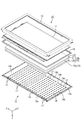
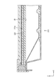
本実施形態に係るテレビ受信装置10TVは、図1に示すように、液晶表示装置10と、当該液晶表示装置10を挟むようにして収容する表裏両キャビネット10Ca,10Cbと、電源10Pと、テレビ信号を受信するチューナー(受信部)10Tと、スタンド10Sと、を備えて構成される。液晶表示装置(表示装置)10は、全体として横長(長手)の方形状(矩形状)をなし、縦置き状態で収容されている。この液晶表示装置10は、図2に示すように、画像を表示する表示パネルである液晶パネル11と、液晶パネル11に表示のための光を供給する外部光源であるバックライト装置(照明装置)12と、を備え、これらが枠状のベゼル13などにより一体的に保持されるようになっている。
As shown in FIG. 1, the television receiver 10TV according to the present embodiment receives a liquid crystal display device 10, front and back cabinets 10Ca and 10Cb that are accommodated so as to sandwich the liquid crystal display device 10, a power supply 10P, and a television signal. And a tuner (reception unit) 10T and a stand 10S. The liquid crystal display device (display device) 10 has a horizontally long (longitudinal) rectangular shape (rectangular shape) as a whole and is accommodated in a vertically placed state. As shown in FIG. 2, the liquid crystal display device 10 includes a liquid crystal panel 11 that is a display panel that displays an image, and a backlight device (illumination device) that is an external light source that supplies light for display to the liquid crystal panel 11. 12 and these are integrally held by a frame-like bezel 13 or the like.
次に、液晶表示装置10を構成する液晶パネル11及びバックライト装置12について順次に説明する。このうち、液晶パネル(表示パネル)11は、平面に視て横長な方形状をなしており、一対のガラス基板が所定のギャップを隔てた状態で貼り合わせられるとともに、両ガラス基板間に液晶が封入された構成とされる。一方のガラス基板(アレイ基板、アクティブマトリクス基板)には、互いに直交するソース配線とゲート配線とに接続されたスイッチング素子(例えばTFT)、そのスイッチング素子に接続された画素電極、さらには配向膜等が設けられ、他方のガラス基板(対向基板、CF基板)には、R(赤色),G(緑色),B(青色)等の各着色部が所定配列で配置されたカラーフィルタや対向電極、さらには配向膜等が設けられている。なお、両ガラス基板の外側にはそれぞれ偏光板が配されている。
Next, the liquid crystal panel 11 and the backlight device 12 constituting the liquid crystal display device 10 will be described sequentially. Among these, the liquid crystal panel (display panel) 11 has a horizontally long rectangular shape when seen in a plan view, and a pair of glass substrates are bonded together with a predetermined gap therebetween, and a liquid crystal is formed between both glass substrates. It is set as the enclosed structure. On one glass substrate (array substrate, active matrix substrate), a switching element (for example, TFT) connected to the source wiring and gate wiring orthogonal to each other, a pixel electrode connected to the switching element, an alignment film, etc. The other glass substrate (counter substrate, CF substrate) has a color filter or counter electrode in which colored portions such as R (red), G (green), and B (blue) are arranged in a predetermined arrangement, Furthermore, an alignment film or the like is provided. A polarizing plate is disposed outside each of the glass substrates.
続いて、バックライト装置12について詳しく説明する。バックライト装置12は、図2に示すように、表側(光出射側、液晶パネル11側)に開口する光出射部14bを有した略箱型をなすシャーシ14と、シャーシ14の光出射部14bを覆うようにして配される光学部材15と、シャーシ14の外縁部に沿って配され光学部材15の外縁部をシャーシ14との間で挟んで保持するフレーム16と、を備える。さらに、シャーシ14内には、LED(光源)17と、LED17が実装されたLED基板18と、シャーシ14内の光を反射させる反射シート(反射部材)19と、が備えられる。このように、本実施形態に係るバックライト装置12は、シャーシ14内において液晶パネル11及び光学部材15の直下位置にLED17が配されてその発光面17aが対向状をなす、いわゆる直下型とされる。以下では、バックライト装置12の各構成部品について詳しく説明する。
Subsequently, the backlight device 12 will be described in detail. As shown in FIG. 2, the backlight device 12 includes a substantially box-shaped chassis 14 having a light emitting portion 14 b that opens on the front side (light emitting side, liquid crystal panel 11 side), and a light emitting portion 14 b of the chassis 14. And an optical member 15 disposed so as to cover the frame, and a frame 16 disposed along the outer edge portion of the chassis 14 and holding the outer edge portion of the optical member 15 between the chassis 14 and the frame 16. Furthermore, in the chassis 14, an LED (light source) 17, an LED substrate 18 on which the LED 17 is mounted, and a reflection sheet (reflecting member) 19 that reflects the light in the chassis 14 are provided. As described above, the backlight device 12 according to the present embodiment is a so-called direct type in which the LED 17 is arranged in the chassis 14 immediately below the liquid crystal panel 11 and the optical member 15 and the light emitting surface 17a is opposed. The Below, each component of the backlight apparatus 12 is demonstrated in detail.
シャーシ14は、例えばアルミニウム板や電気亜鉛めっき綱板(SECC)などの金属板からなり、図3から図5に示すように、液晶パネル11と同様に横長な方形状(矩形状、長方形状)をなす底板部(底部)14aと、底板部14aの各辺(一対の長辺及び一対の短辺)の外端からそれぞれ表側(光出射側)に向けて立ち上がる側板部(側部)14cと、各側板部14cの立ち上がり端から外向きに張り出す受け板部(受け部)14dと、からなり、全体としては表側に向けて開口した浅い略箱型(略浅皿状)をなしている。シャーシ14は、その長辺方向がX軸方向と一致し、短辺方向がY軸方向と一致している。シャーシ14における底板部14aは、LED基板18に対して裏側、つまりLED17に対してその発光面17a側(光出射側)とは反対側に配されている。シャーシ14における各側板部14cは、底板部14aに対して傾斜状をなしている。シャーシ14における各受け板部14dには、表側からフレーム16及び次述する光学部材15が載置可能とされる。各受け板部14dには、フレーム16が固定されている。
The chassis 14 is made of, for example, a metal plate such as an aluminum plate or an electrogalvanized steel plate (SECC). As shown in FIGS. 3 to 5, the chassis 14 has a horizontally long rectangular shape (rectangular shape, rectangular shape) like the liquid crystal panel 11. A bottom plate portion (bottom portion) 14a, and a side plate portion (side portion) 14c rising from the outer end of each side (a pair of long sides and a pair of short sides) toward the front side (light emission side), respectively. And a receiving plate portion (receiving portion) 14d projecting outward from the rising end of each side plate portion 14c, and as a whole has a shallow substantially box shape (substantially shallow dish shape) that opens toward the front side. . The long side direction of the chassis 14 matches the X-axis direction, and the short side direction matches the Y-axis direction. The bottom plate portion 14a of the chassis 14 is disposed on the back side of the LED substrate 18, that is, on the opposite side of the LED 17 from the light emitting surface 17a side (light emitting side). Each side plate portion 14c in the chassis 14 is inclined with respect to the bottom plate portion 14a. A frame 16 and an optical member 15 to be described below can be placed on each receiving plate portion 14d of the chassis 14 from the front side. A frame 16 is fixed to each receiving plate portion 14d.
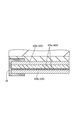
光学部材15は、図2に示すように、液晶パネル11及びシャーシ14と同様に平面に視て横長の方形状をなしている。光学部材15は、図4及び図5に示すように、その外縁部が受け板部14dに載せられることで、シャーシ14の光出射部14bを覆うとともに、液晶パネル11とLED17との間に介在して配される。光学部材15は、LED17の発光面17aに対して表側、つまり光出射側に所定の間隔を空けて対向状をなしている。光学部材15は、相対的に厚い拡散板15aと、相対的に薄い光学シート15bと、から構成される。拡散板15aは、光学シート15bより厚くてほぼ透明な樹脂製の基材内に拡散粒子を多数分散して設けた構成とされ、透過する光を拡散させる機能を有する。拡散板15aは、光学シート15bよりも厚くて十分に高い剛性を有しているから、高い平坦性を有するものとされ、それによりLED17からの光を板面内において均一に拡散させることができる。光学シート15bは、拡散板15aと比べると板厚が薄いシート状をなしており、合計で3枚が備えられている。具体的には、光学シート15bは、LED17から発せられた光(一次光)を他の波長の光へと波長変換する波長変換シート(波長変換部材)20と、光に集光作用を付与するプリズムシート21と、光を偏光反射する反射型偏光シート22と、から構成される。このうちの波長変換シート20に関しては、後に改めて詳しく説明する。
As shown in FIG. 2, the optical member 15 has a horizontally long rectangular shape when viewed in a plane, like the liquid crystal panel 11 and the chassis 14. As shown in FIGS. 4 and 5, the optical member 15 has an outer edge portion placed on the receiving plate portion 14 d so as to cover the light emitting portion 14 b of the chassis 14 and be interposed between the liquid crystal panel 11 and the LED 17. Arranged. The optical member 15 is opposed to the light emitting surface 17a of the LED 17 at a predetermined interval on the front side, that is, on the light emitting side. The optical member 15 includes a relatively thick diffusion plate 15a and a relatively thin optical sheet 15b. The diffusing plate 15a has a structure in which a large number of diffusing particles are dispersed and provided in a substantially transparent resin base material thicker than the optical sheet 15b, and has a function of diffusing transmitted light. The diffusing plate 15a is thicker than the optical sheet 15b and has a sufficiently high rigidity. Therefore, the diffusing plate 15a has high flatness, so that the light from the LED 17 can be uniformly diffused in the plate surface. . The optical sheet 15b has a sheet shape that is thinner than the diffusion plate 15a, and a total of three optical sheets are provided. Specifically, the optical sheet 15b provides a wavelength conversion sheet (wavelength conversion member) 20 that converts the wavelength of light (primary light) emitted from the LED 17 into light of another wavelength, and condenses light. It comprises a prism sheet 21 and a reflective polarizing sheet 22 that reflects and reflects light. Of these, the wavelength conversion sheet 20 will be described in detail later.
プリズムシート21は、基材と、基材における表側の板面に設けられるプリズム部と、を有しており、このうちのプリズム部が、X軸方向に沿って延在するとともにY軸方向に沿って多数並んで配される単位プリズムから構成されている。このような構成により、プリズムシート21は、光に対し、Y軸方向(単位プリズムの並び方向、単位プリズムの延在方向と直交する方向)について選択的に集光作用(異方性集光作用)を付与するものとされる。反射型偏光シート22は、光を偏光反射する反射型偏光フィルムと、反射型偏光フィルムを表裏から挟み込む一対の拡散フィルムと、から構成される。反射型偏光フィルムは、例えば屈折率の互いに異なる層を交互に積層した多層構造を有しており、光に含まれるp波を透過させ、s波を裏側へ反射させる構成となっている。反射型偏光フィルムによって反射されたs波は、後述する反射シート19などによって、再度表側に反射され、その際に、s波とp波に分離する。このように、反射型偏光シート22は、反射型偏光フィルムを備えることで、本来ならば、液晶パネル11の偏光板によって吸収されるs波を、裏側(反射シート19側)へ反射させることで再利用することができ、光の利用効率(ひいては輝度)を高めることができる。一対の拡散フィルムは、ポリカーボネートなどの合成樹脂材料からなり、反射型偏光フィルム側とは反対側の板面にエンボス加工が施されることで、光に拡散作用を付与するものとされる。
The prism sheet 21 has a base material and a prism portion provided on the front plate surface of the base material, and the prism portion of the prism sheet 21 extends along the X-axis direction and extends in the Y-axis direction. It is composed of unit prisms that are arranged alongside each other. With such a configuration, the prism sheet 21 selectively collects light with respect to the light in the Y-axis direction (unit prism arrangement direction, unit prism extending direction). ). The reflective polarizing sheet 22 includes a reflective polarizing film that polarizes and reflects light, and a pair of diffusion films that sandwich the reflective polarizing film from the front and back. The reflective polarizing film has, for example, a multilayer structure in which layers having different refractive indexes are alternately laminated, and has a configuration in which p waves included in light are transmitted and s waves are reflected to the back side. The s wave reflected by the reflective polarizing film is reflected again to the front side by a reflection sheet 19 or the like described later, and at that time, separated into an s wave and a p wave. As described above, the reflective polarizing sheet 22 includes the reflective polarizing film, so that the s-wave absorbed by the polarizing plate of the liquid crystal panel 11 is reflected to the back side (the reflective sheet 19 side). It can be reused, and the light utilization efficiency (and hence the luminance) can be increased. The pair of diffusion films are made of a synthetic resin material such as polycarbonate, and are embossed on a plate surface opposite to the reflective polarizing film side to impart a diffusing action to light.
フレーム16は、図2に示すように、液晶パネル11及び光学部材15の外周縁部に沿う枠状をなしている。このフレーム16と各受け板部14dとの間で光学部材15における外縁部を挟持可能とされている(図4及び図5)。また、このフレーム16は、液晶パネル11における外縁部を裏側から受けることができ、表側に配されるベゼル13との間で液晶パネル11の外縁部を挟持可能とされる(図4及び図5)。
As shown in FIG. 2, the frame 16 has a frame shape along the outer peripheral edge portions of the liquid crystal panel 11 and the optical member 15. An outer edge portion of the optical member 15 can be sandwiched between the frame 16 and each receiving plate portion 14d (FIGS. 4 and 5). The frame 16 can receive the outer edge portion of the liquid crystal panel 11 from the back side, and can sandwich the outer edge portion of the liquid crystal panel 11 with the bezel 13 disposed on the front side (FIGS. 4 and 5). ).
次に、LED17及びLED17が実装されるLED基板18について説明する。LED17は、図4及び図5に示すように、LED基板18上に表面実装されるとともにその発光面17aがLED基板18側とは反対側を向いた、いわゆる頂面発光型とされており、その光軸がZ軸方向、つまり液晶パネル11の表示面(光学部材15の板面)に対する法線方向と一致している。ここで言う「光軸」とは、LED17における発光光のうち、発光強度が最も高い(ピークとなる)光の進行方向と一致する軸のことである。詳しくは、LED17は、図6及び図7に示すように、発光源である青色LED素子(青色発光素子、青色LEDチップ)を、封止材によってケース内に封止してなるものとされる。つまり、このLED17は、青色の単色光を発する青色LEDとされている。そして、LED17から発せられた青色の光は、その一部が詳しくは後述する波長変換シート20によって緑色の光や赤色の光に波長変換されるようになっており、これら波長変換された緑色の光及び赤色の光と、LED17の青色の光と、の加法混色によりバックライト装置12の出射光が概ね白色を呈するものとされる。LED17に備わる青色LED素子は、例えばInGaNなどの半導体材料からなる半導体であり、順方向に電圧が印加されることで青色の波長領域(約420nm~約500nm)に含まれる波長の青色の単色光を発光するものとされる。つまり、LED17の発光光は、この青色LED素子の発光光と同色の単色光とされる。この青色LED素子は、図示しないリードフレームによってケース外に配されたLED基板18における配線パターンに接続される。
Next, the LED 17 and the LED board 18 on which the LED 17 is mounted will be described. As shown in FIGS. 4 and 5, the LED 17 is surface-mounted on the LED substrate 18 and has a light emitting surface 17 a facing the side opposite to the LED substrate 18 side, which is a so-called top-emitting type. The optical axis coincides with the Z-axis direction, that is, the normal direction to the display surface of the liquid crystal panel 11 (the plate surface of the optical member 15). The “optical axis” referred to here is an axis that coincides with the traveling direction of light having the highest light emission intensity (peak) among the light emitted from the LED 17. Specifically, as shown in FIGS. 6 and 7, the LED 17 is formed by sealing a blue LED element (blue light emitting element, blue LED chip), which is a light source, in a case with a sealing material. . That is, the LED 17 is a blue LED that emits blue monochromatic light. A part of the blue light emitted from the LED 17 is wavelength-converted into green light or red light by a wavelength conversion sheet 20 described in detail later. By the additive color mixture of light and red light and the blue light of the LED 17, the light emitted from the backlight device 12 is substantially white. The blue LED element provided in the LED 17 is a semiconductor made of a semiconductor material such as InGaN, for example, and is blue monochromatic light having a wavelength included in a blue wavelength region (about 420 nm to about 500 nm) when a voltage is applied in the forward direction. Is supposed to emit light. That is, the light emitted from the LED 17 is monochromatic light having the same color as the light emitted from the blue LED element. This blue LED element is connected to a wiring pattern on the LED substrate 18 arranged outside the case by a lead frame (not shown).
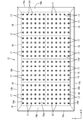
LED基板18は、図3に示すように、やや縦長な方形状(矩形状、長方形状)をなしており、長辺方向がY軸方向と一致し、短辺方向がX軸方向と一致する状態でシャーシ14内において底板部14aに沿って延在しつつ収容されている。LED基板18の基材は、シャーシ14と同じアルミ系材料などの金属製とされ、その表面に絶縁層を介して銅箔などの金属膜からなる配線パターン(図示せず)が形成され、さらには最外表面には、白色を呈する反射層(図示せず)が形成された構成とされる。なお、LED基板18の基材に用いる材料としては、セラミックなどの絶縁材料を用いることも可能である。このLED基板18の基材の板面のうち、表側を向いた板面(光学部材15側を向いた板面)には、上記した構成のLED17が表面実装されており、ここが実装面18aとされる。LED17は、LED基板18の実装面18aの面内において複数ずつ行列状(マトリクス状、碁盤目状)に並列して配されるとともに、実装面18aの面内に配索形成された配線パターンによって相互が電気的に接続されている。具体的には、LED基板18の実装面18a上には、その短辺方向(X軸方向)に沿って5個(相対的に少ない数)ずつ、長辺方向(Y軸方向)に沿って6個(相対的に多い数)ずつのLED17が行列状に並んで配置されている。LED基板18における各LED17の配列ピッチは、ほぼ一定とされ、詳しくはX軸方向(行方向)及びY軸方向(列方向)についてそれぞれほぼ等間隔に配列されている。
As shown in FIG. 3, the LED substrate 18 has a slightly vertical shape (rectangular shape, rectangular shape), the long side direction matches the Y-axis direction, and the short side direction matches the X-axis direction. In the state, it is accommodated in the chassis 14 while extending along the bottom plate portion 14a. The base material of the LED substrate 18 is made of the same metal as the chassis material such as the chassis 14, and a wiring pattern (not shown) made of a metal film such as a copper foil is formed on the surface thereof via an insulating layer. The outermost surface has a configuration in which a white reflective layer (not shown) is formed. In addition, as a material used for the base material of LED board 18, insulating materials, such as a ceramic, can also be used. The LED 17 having the above-described configuration is surface-mounted on the plate surface facing the front side (the plate surface facing the optical member 15 side) among the plate surfaces of the base material of the LED substrate 18, and this is the mounting surface 18a. It is said. The LEDs 17 are arranged in parallel in a matrix (matrix, grid) in the surface of the mounting surface 18a of the LED substrate 18, and by a wiring pattern formed in the surface of the mounting surface 18a. They are electrically connected to each other. Specifically, on the mounting surface 18a of the LED substrate 18, five pieces (relatively few) along the long side direction (Y-axis direction) along the short side direction (X-axis direction). Six (relatively large) LEDs 17 are arranged in a matrix. The arrangement pitch of the LEDs 17 on the LED substrate 18 is substantially constant. Specifically, the LEDs 17 are arranged at substantially equal intervals in the X-axis direction (row direction) and the Y-axis direction (column direction).
上記した構成のLED基板18は、図3に示すように、シャーシ14内においてX軸方向及びY軸方向に沿って複数ずつが互いに長辺方向及び短辺方向を揃えた状態で並列して配置されている。具体的には、LED基板18は、シャーシ14内においてX軸方向に沿って4枚(相対的に多い数)ずつ、Y軸方向に沿って2枚(相対的に少ない数)ずつ、それぞれ並んで配されており、それらの並び方向がX軸方向及びY軸方向とそれぞれ一致している。X軸方向及びY軸方向についてそれぞれ隣り合うLED基板18間の配列間隔は、ほぼ一定とされる。そして、シャーシ14の底板部14aの面内においてLED17は、X軸方向(行方向)及びY軸方向(列方向)についてそれぞれほぼ等間隔となるよう行列状に並ぶよう平面配置されている。具体的には、LED17は、シャーシ14の底板部14aの面内においてその長辺方向(X軸方向)に沿って20個ずつ、短辺方向(Y軸方向)に沿って12個ずつが行列状に並ぶ形で平面配置されている。これらのLED17群の全てに対して、シャーシ14の光出射部14bを覆う形で配された光学部材15は、所定の間隔を空けつつ対向状に配されている。なお、各LED基板18には、図示しない配線部材が接続されるコネクタ部が設けられており、配線部材を介して図示しないLED駆動基板(光源駆動基板)から駆動電力が供給されるようになっている。
As shown in FIG. 3, the LED boards 18 having the above-described configuration are arranged in parallel in the chassis 14 in a state where the long side direction and the short side direction are aligned with each other along the X axis direction and the Y axis direction. Has been. Specifically, the LED boards 18 are arranged in the chassis 14 by four pieces (relatively large numbers) along the X-axis direction and by two pieces (relatively small numbers) along the Y-axis direction. The arrangement directions thereof coincide with the X-axis direction and the Y-axis direction, respectively. The arrangement interval between the LED substrates 18 adjacent to each other in the X-axis direction and the Y-axis direction is substantially constant. In the plane of the bottom plate portion 14a of the chassis 14, the LEDs 17 are arranged in a line so as to be arranged in a matrix so as to be substantially equally spaced in the X axis direction (row direction) and the Y axis direction (column direction). Specifically, 20 LEDs 17 along the long side direction (X-axis direction) and 12 LEDs 17 along the short side direction (Y-axis direction) in the plane of the bottom plate portion 14a of the chassis 14 are arranged in a matrix. They are arranged in a plane in a line. The optical member 15 disposed so as to cover the light emitting portion 14b of the chassis 14 is disposed in an opposing manner with respect to all of the LEDs 17 group with a predetermined interval. Each LED board 18 is provided with a connector portion to which a wiring member (not shown) is connected, and driving power is supplied from an LED driving board (light source driving board) (not shown) via the wiring member. ing.
反射シート19は、合成樹脂製とされ、表面が光の反射性に優れた白色を呈するものとされる。反射シート19は、その表面にて特定の波長の光を吸収することがなく、全ての可視光線を乱反射するものとされており、全域にわたって光の反射率がほぼ一定とされている。反射シート19は、図3から図5に示すように、シャーシ14の内面のほぼ全域にわたって敷設される大きさを有しているので、シャーシ14内に配されたLED基板18をほぼ全域にわたって表側(光出射側、光学部材15側)から覆うことが可能とされる。この反射シート19によりシャーシ14内の光を表側(光出射側、光学部材15側)に向けて反射させることができるようになっている。反射シート19は、LED基板18(底板部14a)に沿って延在するとともに各LED基板18を一括してそのほぼ全域を覆う大きさの底側反射部19aと、底側反射部19aの各外端から表側に立ち上がるとともに底側反射部19aに対して傾斜状をなす4つの立ち上がり反射部19bと、各立ち上がり反射部19bの外端から外向きに延出するとともにシャーシ14の受け板部14dに載せられる延出部19cとから構成されている。この反射シート19の底側反射部19aが各LED基板18における表側の面、つまりLED17の実装面18aに対して表側に重なるよう配される。また、反射シート19の底側反射部19aには、各LED17と平面に視て重畳する位置に各LED17を個別に挿通するLED挿通孔(光源挿通孔)19dが開口して設けられている。このLED挿通孔19dは、各LED17の配置に対応してX軸方向及びY軸方向について行列状(マトリクス状)に複数が並列配置されている。各立ち上がり反射部19bは、底側反射部19a側(立ち上がり基端側)からシャーシ14の受け板部14d側(立ち上がり先端側)に向けて直線的に延在する形で底側反射部19aに対して傾斜状をなしている。
The reflection sheet 19 is made of a synthetic resin and has a white surface with excellent light reflectivity. The reflection sheet 19 does not absorb light of a specific wavelength on the surface thereof, and diffusely reflects all visible rays, and the light reflectance is substantially constant over the entire area. As shown in FIGS. 3 to 5, the reflection sheet 19 has a size that is laid over almost the entire inner surface of the chassis 14, so that the LED board 18 disposed in the chassis 14 is almost entirely on the front side. It is possible to cover from (light emitting side, optical member 15 side). The reflection sheet 19 can reflect the light in the chassis 14 toward the front side (light emission side, optical member 15 side). The reflection sheet 19 extends along the LED substrate 18 (bottom plate portion 14a), and each of the bottom-side reflection portion 19a and the bottom-side reflection portion 19a have a size that covers each LED substrate 18 in a lump. Four rising reflecting portions 19b that rise from the outer end to the front side and are inclined with respect to the bottom reflecting portion 19a, and extend outward from the outer ends of the respective rising reflecting portions 19b and receive plate portions 14d of the chassis 14 It is comprised from the extension part 19c mounted on. The bottom reflection part 19 a of the reflection sheet 19 is arranged so as to overlap the front side of each LED substrate 18, that is, the mounting surface 18 a of the LED 17. In addition, an LED insertion hole (light source insertion hole) 19 d through which each LED 17 is individually inserted is provided in the bottom side reflection portion 19 a of the reflection sheet 19 at a position overlapping with each LED 17 in plan view. A plurality of the LED insertion holes 19d are arranged in parallel in a matrix (matrix shape) in the X-axis direction and the Y-axis direction corresponding to the arrangement of the LEDs 17. Each rising reflecting portion 19b extends from the bottom reflecting portion 19a (rising base end side) to the bottom reflecting portion 19a in a form extending linearly from the receiving plate portion 14d side (rising leading end side) of the chassis 14. On the other hand, it is inclined.
次に、波長変換シート20に関して詳しく説明する。波長変換シート20は、図8に示すように、LED17からの光を波長変換するための蛍光体(波長変換物質)を含有する蛍光体層(波長変換層、蛍光体フィルム)20aと、蛍光体層20aを表裏から挟み込んでこれを保護する一対の保護層(保護フィルム)20bと、から構成されている。蛍光体層20aには、LED17からの青色の単色光を励起光として、赤色の光(赤色に属する特定の波長領域の可視光線)を発する赤色蛍光体と、緑色(緑色に属する特定の波長領域の可視光線)の光を発する緑色蛍光体と、が分散配合されている。蛍光体層20aは、ほぼ透明な合成樹脂製でフィルム状をなす基材(蛍光体担体)20a1に、赤色蛍光体及び緑色蛍光体を分散配合した蛍光体塗料20a2を塗布してなるものとされる。保護層20bは、ほぼ透明な合成樹脂製でフィルム状をなしており、防湿性などに優れるものとされる。
Next, the wavelength conversion sheet 20 will be described in detail. As shown in FIG. 8, the wavelength conversion sheet 20 includes a phosphor layer (wavelength conversion layer, phosphor film) 20a containing a phosphor (wavelength conversion substance) for wavelength-converting light from the LED 17, and a phosphor. It is comprised from a pair of protective layer (protective film) 20b which pinches | interposes the layer 20a from the front and back, and protects this. The phosphor layer 20a includes a red phosphor that emits red light (visible light in a specific wavelength region belonging to red) using blue monochromatic light from the LED 17 as excitation light, and green (a specific wavelength region belonging to green). And a green phosphor emitting light of visible light). The phosphor layer 20a is formed by applying a phosphor coating material 20a2 in which a red phosphor and a green phosphor are dispersed and mixed to a base material (phosphor carrier) 20a1 made of a substantially transparent synthetic resin to form a film. The The protective layer 20b is made of a substantially transparent synthetic resin and has a film shape, and is excellent in moisture resistance and the like.
より詳しくは、蛍光体層20aに含有される各色の蛍光体は、いずれも励起光が青色の光とされており、次のような発光スペクトルを有している。すなわち、緑色蛍光体は、青色の光を励起光として、緑色に属する波長領域(約500nm~約570nm)の光、つまり緑色の光を蛍光光として発するものとされる。緑色蛍光体は、好ましくは、ピークのピーク波長が緑色の光の波長範囲の中の約530nmとされ且つピークの半値幅が40nm未満とされる発光スペクトルを有する。赤色蛍光体は、青色の光を励起光として、赤色に属する波長領域(約600nm~約780nm)の光、つまり赤色の光を蛍光光として発するものとされる。赤色蛍光体は、好ましくは、ピークのピーク波長が赤色の光の波長範囲の中の約610nmとされ且つピークの半値幅が40nm未満とされる発光スペクトルを有する。
More specifically, each of the phosphors of each color contained in the phosphor layer 20a has blue excitation light and has the following emission spectrum. That is, the green phosphor emits blue light as excitation light and emits light in a wavelength region (about 500 nm to about 570 nm) belonging to green, that is, green light as fluorescence light. The green phosphor preferably has an emission spectrum in which the peak wavelength of the peak is about 530 nm in the wavelength range of green light and the half width of the peak is less than 40 nm. The red phosphor emits blue light as excitation light and emits light in a wavelength region (about 600 nm to about 780 nm) belonging to red, that is, red light as fluorescent light. The red phosphor preferably has an emission spectrum in which the peak wavelength of the peak is about 610 nm within the wavelength range of red light, and the half width of the peak is less than 40 nm.
このように、各色の蛍光体は、励起波長が蛍光波長よりも短波長とされるダウンコンバージョン型(ダウンシフティング型)とされている。このダウンコンバージョン型の蛍光体は、相対的に短波長で且つ高いエネルギーを持つ励起光を、相対的に長波長で且つ低いエネルギーを持つ蛍光光に変換するものとされる。従って、仮に励起波長が蛍光波長よりも長波長とされるアップコンバージョン型の蛍光体を用いた場合(量子効率が例えば28%程度)に比べると、量子効率(光の変換効率)が30%~50%程度と、より高いものとなっている。各色の蛍光体は、それぞれ量子ドット蛍光体(Quantum Dot Phosphor)とされる。量子ドット蛍光体は、ナノサイズ(例えば直径2nm~10nm程度)の半導体結晶中に電子・正孔や励起子を三次元空間全方位で閉じ込めることで、離散的エネルギー準位を有しており、そのドットのサイズを変えることで発光光のピーク波長(発光色)などを適宜に選択することが可能とされる。この量子ドット蛍光体の発光光(蛍光光)は、その発光スペクトルにおけるピークが急峻となってその半値幅が狭くなることから、色純度が極めて高くなるとともにその色域が広いものとなる。量子ドット蛍光体の材料としては、2価の陽イオンになるZn、Cd、Hg、Pb等と2価の陰イオンになるO、S、Se、Te等とを組み合わせた材料(CdSe(セレン化カドミウム)、ZnS(硫化亜鉛)等)、3価の陽イオンとなるGa、In等と3価の陰イオンとなるP、As、Sb等とを組み合わせた材料(InP(リン化インジウム)、GaAs(ヒ化ガリウム)等)、さらにはカルコパイライト型化合物(CuInSe2等)などがある。本実施形態では、量子ドット蛍光体の材料として、上記のうちのCdSeとZnSとを併用している。また、本実施形態において用いる量子ドット蛍光体は、いわゆるコア・シェル型量子ドット蛍光体とされる。コア・シェル型量子ドット蛍光体は、量子ドットの周囲を、比較的バンドギャップの大きな半導体物質からなるシェルによって被覆した構成とされる。具体的には、コア・シェル型量子ドット蛍光体として、シグマ アルドリッチ ジャパン合同会社の製品である「Lumidot(登録商標) CdSe/ZnS」を用いるのが好ましい。
Thus, the phosphors of the respective colors are of the down conversion type (down shifting type) in which the excitation wavelength is shorter than the fluorescence wavelength. This down-conversion type phosphor is supposed to convert excitation light having a relatively short wavelength and high energy into fluorescence light having a relatively long wavelength and low energy. Therefore, the quantum efficiency (light conversion efficiency) is 30% to 30% higher than when using an up-conversion type phosphor whose excitation wavelength is longer than the fluorescence wavelength (quantum efficiency is about 28%, for example). It is about 50% and higher. Each color phosphor is a quantum dot phosphor (Quantum Dot Phosphor). Quantum dot phosphors have discrete energy levels by confining electrons, holes, and excitons in all three-dimensional space in a nano-sized semiconductor crystal (for example, about 2 nm to 10 nm in diameter) By changing the size of the dots, the peak wavelength (emission color) of emitted light can be appropriately selected. The emission light (fluorescence light) of the quantum dot phosphor has a sharp peak in the emission spectrum and a narrow half width, so that the color purity is extremely high and the color gamut is wide. As a material of the quantum dot phosphor, a combination of Zn, Cd, Hg, Pb or the like that becomes a divalent cation and O, S, Se, Te, or the like that becomes a divalent anion (CdSe (selenization) (Cadmium), ZnS (Zinc Sulfide), etc.) A material (InP (Indium Phosphide), GaAs) that combines trivalent cation Ga, In, etc. with trivalent anion P, As, Sb, etc. (Gallium arsenide) and the like) and chalcopyrite type compounds (CuInSe 2 and the like). In this embodiment, CdSe and ZnS among the above are used in combination as the material of the quantum dot phosphor. The quantum dot phosphor used in the present embodiment is a so-called core-shell type quantum dot phosphor. The core-shell type quantum dot phosphor has a configuration in which the periphery of the quantum dot is covered with a shell made of a semiconductor material having a relatively large band gap. Specifically, it is preferable to use “Lumidot (registered trademark) CdSe / ZnS”, which is a product of Sigma Aldrich Japan LLC, as the core-shell type quantum dot phosphor.
ところで、LED17の青色の光を波長変換するための波長変換シート20は、図8に示すように、蛍光体層20aを一対の保護層20bで挟む込んだ構成とされることで、蛍光体層20aの保護が図られているものの、蛍光体層20aの外周端については外気に含まれる水分などに曝され易いものとなっている。このため、蛍光体層20aのうち外周側部分では、中央側部分に比べると、含有する各蛍光体に吸湿などによる劣化が生じ易いものとなっている。この蛍光体の性能劣化は、蛍光体層20aの外周端に封止などの防湿措置が採られていない構成において特に生じ易いものとされる。そして、波長変換シート20の外周側部分において局所的に各蛍光体の性能劣化が進行すると、その外周側部分における光の波長変換効率が中央側部分の同波長変換効率よりも低下するため、外周側部分を透過した光が、中央側部分を透過した光よりもLED17の光(一次光)と同系色の色味、つまり青色味を帯びたものとなるおそれがある。つまり、バックライト装置12の出射光が中央側では白色に近いものの、外周側ではそれよりも青色味を帯びたものとなる、という色ムラが視認されることが懸念される。波長変換シート20のうち上記のような色ムラが生じ得る外周側部分は、平面に視て所定幅の枠状(額縁状)をなすものとされており、具体的に色ムラとなる部分の範囲(幅寸法)は、防湿措置の有無、使用環境(温度や湿度など)、各蛍光体の物性(耐吸湿性など)などの諸条件に応じて変動し得るものとされるが、画像が表示される表示領域にまで及ぶと、表示不良が発現するおそれがある。
By the way, the wavelength conversion sheet 20 for converting the wavelength of the blue light of the LED 17 is configured such that the phosphor layer 20a is sandwiched between a pair of protective layers 20b as shown in FIG. Although protection of 20a is achieved, the outer peripheral end of the phosphor layer 20a is easily exposed to moisture contained in the outside air. For this reason, in the outer peripheral portion of the phosphor layer 20a, the phosphors contained therein are more likely to be deteriorated due to moisture absorption or the like than in the central portion. This deterioration in the performance of the phosphor is particularly likely to occur in a configuration in which moisture-proof measures such as sealing are not taken at the outer peripheral end of the phosphor layer 20a. And when the performance deterioration of each phosphor proceeds locally in the outer peripheral side portion of the wavelength conversion sheet 20, the wavelength conversion efficiency of light in the outer peripheral side portion is lower than the same wavelength conversion efficiency in the central side portion. There is a possibility that the light transmitted through the side portion has a color similar to that of the light of the LED 17 (primary light), i.e., a blue tint, than the light transmitted through the central side portion. That is, there is a concern that the color unevenness in which the emitted light of the backlight device 12 is close to white on the center side but becomes more bluish on the outer peripheral side is visible. The outer peripheral portion of the wavelength conversion sheet 20 where color unevenness as described above may occur has a frame shape (frame shape) with a predetermined width when seen in a plan view. The range (width dimension) may vary depending on various conditions such as the presence or absence of moisture-proof measures, the usage environment (temperature, humidity, etc.), and the physical properties of each phosphor (moisture absorption resistance, etc.). If it extends to the display area to be displayed, a display defect may occur.
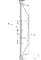
そこで、本実施形態に係るバックライト装置12は、図6及び図7に示すように、拡散板15aが波長変換シート20に対して表側、つまり出光側に配される構成となっている。このような構成によれば、波長変換シート20の外周側部分において各蛍光体が吸湿などによって劣化し、波長変換シート20の外周側部分を透過した光の色味と、波長変換シート20の中央側部分を透過した光の色味と、に差が生じていた場合であっても、それらの透過光には表側に配された拡散板15aによって拡散作用が付与され、その上でバックライト装置12の照明光として出射されることになる。従って、バックライト装置12の出射光には、中央側と外周側とで色味の差が生じ難くなり、もって色ムラが視認され難いものとなる。特に、本実施形態では、波長変換シート20に含有される緑色蛍光体及び赤色蛍光体が共に量子ドット蛍光体とされ、他の種類の蛍光体に比べると吸湿などによって性能劣化が生じ易く、波長変換シート20の外周側部分において波長変換効率が低下し易い傾向にあるものの、上記のように波長変換シート20の透過光が拡散板15aによる拡散されることで、発生が懸念される色ムラが効果的に抑制されるようになっている。
Therefore, as shown in FIGS. 6 and 7, the backlight device 12 according to the present embodiment has a configuration in which the diffusion plate 15 a is arranged on the front side, that is, the light output side with respect to the wavelength conversion sheet 20. According to such a configuration, each phosphor deteriorates due to moisture absorption or the like in the outer peripheral portion of the wavelength conversion sheet 20, and the color of light transmitted through the outer peripheral portion of the wavelength conversion sheet 20 and the center of the wavelength conversion sheet 20. Even if there is a difference in the color of the light transmitted through the side portion, the transmitted light is given a diffusing action by the diffusion plate 15a arranged on the front side, and then the backlight device It will be emitted as 12 illumination lights. Accordingly, in the emitted light from the backlight device 12, a difference in color is less likely to occur between the central side and the outer peripheral side, and color unevenness is less likely to be visually recognized. In particular, in the present embodiment, both the green phosphor and the red phosphor contained in the wavelength conversion sheet 20 are quantum dot phosphors, and performance degradation is likely to occur due to moisture absorption or the like compared to other types of phosphors. Although there is a tendency that the wavelength conversion efficiency tends to be reduced at the outer peripheral side portion of the conversion sheet 20, the color unevenness that is likely to occur due to the diffusion of the transmitted light of the wavelength conversion sheet 20 by the diffusion plate 15 a as described above. It is designed to be effectively suppressed.
詳しくは、波長変換シート20は、図6及び図7に示すように、拡散板15aのうち裏側、つまり出光側とは反対側の板面に貼り付けられている。これにより、波長変換シート20の平坦性を拡散板15aによって担保することができる。その上で、波長変換シート20は、拡散板15aとの間に介在する接着層23によって接着されている。接着層23は、例えばOCA(Optical Clear Adhesive)などの透明光学粘着フィルムからなるものとされている。このようにすれば、波長変換シート20の透過光が波長変換シート20と接着層23との間の界面や接着層23と拡散板15aとの界面にて反射されるなどして再び波長変換シート20を通過し易くなるので、波長変換シート20の各蛍光体による光の波長変換効率がより高いものとなる。しかも、拡散板15aは、平面に視た大きさが波長変換シート20とほぼ同じ程度とされており、波長変換シート20をその全域にわたって表側から覆う形で配されている。このような構成によれば、波長変換シート20の中央側部分及び外周側部分の透過光に対して拡散板15aによって拡散作用が万遍なく付与されるので、色ムラがより生じ難いものとなる。
Specifically, as shown in FIGS. 6 and 7, the wavelength conversion sheet 20 is attached to the back side of the diffusion plate 15a, that is, the plate surface opposite to the light output side. Thereby, the flatness of the wavelength conversion sheet 20 can be ensured by the diffusion plate 15a. In addition, the wavelength conversion sheet 20 is adhered by an adhesive layer 23 interposed between the diffusion plate 15a. The adhesive layer 23 is made of a transparent optical adhesive film such as OCA (Optical Clear Adhesive). In this way, the transmitted light of the wavelength conversion sheet 20 is reflected again at the interface between the wavelength conversion sheet 20 and the adhesive layer 23 or at the interface between the adhesive layer 23 and the diffusion plate 15a. Therefore, the wavelength conversion efficiency of light by each phosphor of the wavelength conversion sheet 20 becomes higher. Moreover, the size of the diffusing plate 15a when viewed in a plane is approximately the same as that of the wavelength conversion sheet 20, and is disposed in a form that covers the wavelength conversion sheet 20 from the front side over the entire area. According to such a configuration, the diffusion action is uniformly applied to the transmitted light of the central side portion and the outer peripheral side portion of the wavelength conversion sheet 20 by the diffusion plate 15a, so that color unevenness is less likely to occur. .
具体的な光学部材15の積層順は、図6及び図7に示すように、裏側から、波長変換シート20、拡散板15a、プリズムシート21、反射型偏光シート22、となっている。つまり、拡散板15aの表側には、拡散板15aよりも薄い光学シート15bであるプリズムシート21及び反射型偏光シート22が順次に積層する形で配されている。拡散板15aは、プリズムシート21及び反射型偏光シート22などの光学シート15bに比べると、厚くて高い剛性を有しているので、拡散板15a上に直接プリズムシート21及び反射型偏光シート22を載せる配置とすることで、プリズムシート21及び反射型偏光シート22の平坦性を十分に担保することができる。
The specific stacking order of the optical members 15 is, as shown in FIGS. 6 and 7, from the back side, the wavelength conversion sheet 20, the diffusion plate 15a, the prism sheet 21, and the reflective polarizing sheet 22. That is, on the front side of the diffusion plate 15a, the prism sheet 21 and the reflective polarizing sheet 22, which are optical sheets 15b thinner than the diffusion plate 15a, are sequentially stacked. The diffusing plate 15a is thicker and has higher rigidity than the optical sheet 15b such as the prism sheet 21 and the reflective polarizing sheet 22, so the prism sheet 21 and the reflective polarizing sheet 22 are provided directly on the diffusing plate 15a. By adopting the placement, the flatness of the prism sheet 21 and the reflective polarizing sheet 22 can be sufficiently secured.
本実施形態は以上のような構造であり、続いてその作用を説明する。液晶表示装置10の電源が投入されると、図示しないコントロール基板から出力される表示に係る各種信号が液晶パネル11へと伝送されることで、液晶パネル11の駆動が制御されるとともに、図示しないLED駆動基板によりLED基板18のLED17の駆動が制御される。点灯されたLED17からの光は、図4及び図5に示すように、直接的に光学部材15に照射されたり、反射シート19により反射されて間接的に光学部材15に照射されたりして光学部材15にて所定の光学作用が付与された後に液晶パネル11へと照射されることで、液晶パネル11の表示領域にて画像の表示に利用される。
This embodiment has the structure as described above, and its operation will be described next. When the power of the liquid crystal display device 10 is turned on, various signals relating to display output from a control board (not shown) are transmitted to the liquid crystal panel 11, thereby controlling the driving of the liquid crystal panel 11 and not shown. The driving of the LEDs 17 on the LED board 18 is controlled by the LED driving board. As shown in FIGS. 4 and 5, the light from the LED 17 that has been lit is directly applied to the optical member 15, or reflected by the reflection sheet 19 and indirectly applied to the optical member 15. The liquid crystal panel 11 is irradiated after a predetermined optical action is given by the member 15, and is used for displaying an image in the display area of the liquid crystal panel 11.
バックライト装置12の光学作用(但し、後述する拡散板15a及び波長変換シート20の詳しい光学作用などを除く)について詳しく説明すると、図4及び図5に示すように、LED17から発せられた青色の光(一次光)は、光学部材15を構成する拡散板15a及び光学シート15bによって光学作用を付与される。光学シート15bには、波長変換シート20が含まれているので、LED17から発せられた青色の光の一部については、波長変換シート20に含有される緑色蛍光体及び赤色蛍光体により緑色の光及び赤色の光(二次光)へと波長変換される。この波長変換された緑色の光及び赤色の光、つまり黄色の光(二次光)と、LED17の青色の光(一次光)と、によって概ね白色の照明光が得られることになる。これらLED17の青色の光(一次光)と、波長変換された緑色の光及び赤色の光(二次光)と、は、プリズムシート21にてY軸方向について選択的に集光作用(異方性集光作用)が付与された後に、反射型偏光シート22にて特定の偏光光(p波)が選択的に透過されて液晶パネル11に向けて出射するのに対し、それとは異なる特定の偏光光(s波)が選択的に裏側へと反射される。反射型偏光シート22にて反射されたs波やプリズムシート21にて集光作用を付与されずに裏側へと反射された光や拡散板15aにて裏側へ向けて反射された光などは、反射シート19にて再び反射されて再び表側へ向けて進行することになる。
The optical action of the backlight device 12 (except for the detailed optical action of the diffuser plate 15a and the wavelength conversion sheet 20 described later) will be described in detail. As shown in FIGS. 4 and 5, the blue light emitted from the LED 17 is emitted. The light (primary light) is given an optical action by the diffusion plate 15a and the optical sheet 15b constituting the optical member 15. Since the optical sheet 15 b includes the wavelength conversion sheet 20, a part of the blue light emitted from the LED 17 is converted into green light by the green phosphor and the red phosphor contained in the wavelength conversion sheet 20. And wavelength conversion to red light (secondary light). The wavelength-converted green light and red light, that is, yellow light (secondary light) and the blue light (primary light) of the LED 17 provide substantially white illumination light. The blue light (primary light) of the LED 17 and the wavelength-converted green light and red light (secondary light) are selectively condensed (anisotropic) in the Y-axis direction by the prism sheet 21. Specific polarization light (p wave) is selectively transmitted by the reflective polarizing sheet 22 and emitted toward the liquid crystal panel 11, while a specific different from that is given. Polarized light (s wave) is selectively reflected to the back side. The s-wave reflected by the reflective polarizing sheet 22, light reflected by the prism sheet 21 without being condensed, light reflected by the diffuser plate 15a, The light is reflected again by the reflection sheet 19 and travels again toward the front side.
次に、拡散板15a及び波長変換シート20の光学作用について詳しく説明する。波長変換シート20は、光学部材15の中でも最も裏側、つまりLED17に近い側に配されているので、LED17からの青色の光(一次光)が直接的に、或いは反射シート19により反射されて間接的に照射されるようになっている。波長変換シート20は、図8に示すように、一対の保護層20bにより挟み込まれた蛍光体層20aに緑色蛍光体及び赤色蛍光体を有しているので、それら緑色蛍光体及び赤色蛍光体によって上記したLED17からの青色の光を緑色の光及び赤色の光(二次光)へと波長変換するものとされる。ここで、波長変換シート20の外周側部分は、中央側部分に比べると、蛍光体層20aの外周端が外気に含まれる水分などに曝され易いため、緑色蛍光体及び赤色蛍光体に吸湿などに伴う性能劣化が生じ易いものとなっている。このため、波長変換シート20の外周側部分では、中央側部分に比べると、緑色蛍光体及び赤色蛍光体による青色の光の波長変換効率が低下していて透過光に含まれる青色の光の比率が高くなるため、同透過光が相対的に青色味を帯びたものとなり易くなっている。その点、波長変換シート20に対して出光側には、波長変換シート20よりも厚い拡散板15aが重なる形で配されているから、波長変換シート20の透過光に上記のような色ムラが生じていた場合であっても、その透過光を拡散板15aによって拡散することで、波長変換シート20の外周側部分を透過した光と中央側部分を透過した光とが混じり合い、結果として拡散板15aの出射光に色ムラが生じ難いものとなる。これにより、液晶パネル11の表示領域に表示される画像(テレビ画像)に係る表示品位が低下し難いものとなる。
Next, the optical action of the diffusion plate 15a and the wavelength conversion sheet 20 will be described in detail. Since the wavelength conversion sheet 20 is arranged on the back side of the optical member 15, that is, the side closest to the LED 17, the blue light (primary light) from the LED 17 is reflected directly or indirectly by the reflection sheet 19. It comes to be irradiated. As shown in FIG. 8, the wavelength conversion sheet 20 has a green phosphor and a red phosphor in a phosphor layer 20a sandwiched between a pair of protective layers 20b. The wavelength of the blue light from the LED 17 is converted into green light and red light (secondary light). Here, the outer peripheral side portion of the wavelength conversion sheet 20 is more likely to be exposed to moisture contained in the outside air than the central side portion, so that the green phosphor and the red phosphor absorb moisture. It is easy for performance degradation to occur. For this reason, in the outer peripheral part of the wavelength conversion sheet 20, the wavelength conversion efficiency of blue light by the green phosphor and the red phosphor is lower than the central part, and the ratio of the blue light contained in the transmitted light Therefore, the transmitted light tends to have a relatively blue tinge. In that respect, since the diffuser plate 15a thicker than the wavelength conversion sheet 20 is arranged on the light output side with respect to the wavelength conversion sheet 20, the above-described color unevenness is caused in the transmitted light of the wavelength conversion sheet 20. Even if it has occurred, the light transmitted through the outer peripheral side portion of the wavelength conversion sheet 20 and the light transmitted through the central side portion are mixed by diffusing the transmitted light by the diffusion plate 15a, resulting in diffusion. Color unevenness is unlikely to occur in the light emitted from the plate 15a. As a result, the display quality of the image (television image) displayed in the display area of the liquid crystal panel 11 is unlikely to deteriorate.
しかも、波長変換シート20は、図6及び図7に示すように、拡散板15aのうち裏側の板面に接着層23を介して貼り付けられているから、拡散板15aにより高い平坦性が担保されるのに加えて、波長変換シート20の透過光が波長変換シート20と接着層23との間の界面や接着層23と拡散板15aとの界面にて反射されるなどして再び波長変換シート20を通過し易くなるので、波長変換シート20の各蛍光体による光の波長変換効率がより高いものとなる。具体的には、波長変換シート20の各蛍光体による光の波長変換効率は、例えば3%~5%程度向上するものとされる。また、波長変換シート20が高い平坦性を担保されることで、波長変換シート20に皺などの変形が生じ難くなるので、輝度ムラが生じ難いものとなる。さらには、拡散板15aは、波長変換シート20をその全域にわたって表側から覆う形で配されているので、波長変換シート20の中央側部分及び外周側部分の透過光に対して拡散板15aによって拡散作用が万遍なく付与され、もって色ムラがより生じ難いものとなる。その上、拡散板15aの表側には、プリズムシート21及び反射型偏光シート22が順次に積層する形で配されているから、プリズムシート21及び反射型偏光シート22の平坦性が拡散板15aによって十分に担保されるようになっている。これにより、プリズムシート21及び反射型偏光シート22に皺などの変形が生じ難くなるので、輝度ムラが生じ難いものとなる。
In addition, as shown in FIGS. 6 and 7, the wavelength conversion sheet 20 is attached to the back surface of the diffusion plate 15a via the adhesive layer 23, so that high flatness is ensured by the diffusion plate 15a. In addition, the transmitted light of the wavelength conversion sheet 20 is reflected again at the interface between the wavelength conversion sheet 20 and the adhesive layer 23 or at the interface between the adhesive layer 23 and the diffusion plate 15a. Since it becomes easy to pass the sheet | seat 20, the wavelength conversion efficiency of the light by each fluorescent substance of the wavelength conversion sheet 20 becomes a higher thing. Specifically, the wavelength conversion efficiency of light by each phosphor of the wavelength conversion sheet 20 is improved by about 3% to 5%, for example. Moreover, since the wavelength conversion sheet 20 is ensured to have high flatness, the wavelength conversion sheet 20 is less likely to be deformed, such as wrinkles, so that luminance unevenness is less likely to occur. Furthermore, since the diffusing plate 15a is arranged so as to cover the wavelength conversion sheet 20 from the front side over the entire area, the diffusing plate 15a diffuses the transmitted light of the central side portion and the outer peripheral side portion of the wavelength conversion sheet 20 by the diffusing plate 15a. The action is applied evenly, and color unevenness is less likely to occur. In addition, since the prism sheet 21 and the reflective polarizing sheet 22 are sequentially stacked on the front side of the diffusion plate 15a, the flatness of the prism sheet 21 and the reflective polarizing sheet 22 is determined by the diffusion plate 15a. It has come to be fully secured. As a result, deformation such as wrinkles is less likely to occur in the prism sheet 21 and the reflective polarizing sheet 22, so that luminance unevenness is unlikely to occur.
以上説明したように本実施形態のバックライト装置(照明装置)12は、LED(光源)17と、LED17からの光を波長変換する蛍光体を含有する波長変換シート(波長変換部材)20と、LED17からの光に拡散作用を付与する拡散板15aであって、波長変換シート20よりも厚く、波長変換シート20に対して出光側に配される拡散板15aと、を備える。
As described above, the backlight device (illumination device) 12 of the present embodiment includes an LED (light source) 17, a wavelength conversion sheet (wavelength conversion member) 20 containing a phosphor that converts the wavelength of light from the LED 17, and A diffusing plate 15a that imparts a diffusing action to the light from the LED 17 and is thicker than the wavelength converting sheet 20 and is provided on the light output side with respect to the wavelength converting sheet 20.
このようにすれば、LED17からの光は、拡散板15aにより拡散作用が付与されるとともに波長変換シート20に含有される蛍光体によって波長変換されて出射される。拡散板15aは、波長変換シート20よりも厚いから、高い平坦性を有するものとされ、それによりLED17からの光を板面内において均一に拡散させることができる。そして、拡散板15aは、波長変換シート20に対して出光側に配されているから、例えば、波長変換シート20の外周側部分において蛍光体が吸湿などによって劣化し、波長変換シート20の外周側部分を透過した光の色味と、中央側部分を透過した光の色味と、に差が生じていた場合であっても、それらの透過光には拡散板15aによって拡散作用が付与された上で出射されることになるので、その出射光には中央側と外周側とで色味の差が生じ難くなる。これにより、色ムラが生じ難いものとなる。
In this way, the light from the LED 17 is given a diffusing action by the diffusion plate 15a and is wavelength-converted by the phosphor contained in the wavelength conversion sheet 20 and emitted. Since the diffusing plate 15a is thicker than the wavelength conversion sheet 20, the diffusing plate 15a has high flatness, so that the light from the LED 17 can be uniformly diffused in the plate surface. Since the diffusion plate 15a is disposed on the light output side with respect to the wavelength conversion sheet 20, for example, the phosphor deteriorates due to moisture absorption or the like in the outer peripheral side portion of the wavelength conversion sheet 20, and the outer peripheral side of the wavelength conversion sheet 20 Even if there is a difference between the color of the light transmitted through the portion and the color of the light transmitted through the central side portion, the diffused plate 15a imparts a diffusing action to the transmitted light. Since the light is emitted from above, a difference in color is less likely to occur between the central side and the outer peripheral side of the emitted light. As a result, color unevenness hardly occurs.
また、波長変換シート20は、拡散板15aのうち出光側とは反対側の板面に貼り付けられている。このようにすれば、波長変換シート20の平坦性を拡散板15aによって担保することができる。
Further, the wavelength conversion sheet 20 is affixed to the plate surface of the diffusion plate 15a opposite to the light output side. In this way, the flatness of the wavelength conversion sheet 20 can be secured by the diffusion plate 15a.
また、波長変換シート20と拡散板15aとの間には、接着層23が介在する形で設けられている。このようにすれば、波長変換シート20の透過光が波長変換シート20と接着層23との間の界面や接着層23と拡散板15aとの界面にて反射されて再び波長変換シート20を通過し易くなるので、波長変換シート20の蛍光体による波長変換効率がより高いものとなる。
Further, an adhesive layer 23 is provided between the wavelength conversion sheet 20 and the diffusion plate 15a. If it does in this way, the transmitted light of the wavelength conversion sheet 20 will be reflected in the interface between the wavelength conversion sheet 20 and the contact bonding layer 23, and the interface between the contact bonding layer 23 and the diffusion plate 15a, and will pass through the wavelength conversion sheet 20 again. Therefore, the wavelength conversion efficiency by the phosphor of the wavelength conversion sheet 20 becomes higher.
また、拡散板15aに対して出光側には、拡散板15aよりも薄い光学シート15bであるプリズムシート21及び反射型偏光シート22が重なる形で配されている。このようにすれば、光学シート15bであるプリズムシート21及び反射型偏光シート22の平坦性を拡散板15aによって担保することができる。
The prism sheet 21 and the reflective polarizing sheet 22 which are optical sheets 15b thinner than the diffusion plate 15a are arranged on the light output side with respect to the diffusion plate 15a. In this way, the flatness of the prism sheet 21 and the reflective polarizing sheet 22 as the optical sheet 15b can be ensured by the diffusion plate 15a.
また、拡散板15aは、波長変換シート20をその全域にわたって出光側から覆う形で配されている。このようにすれば、波長変換シート20の透過光に対して拡散板15aによって拡散作用が悉に付与されるので、色ムラがより生じ難いものとなる。
Further, the diffusing plate 15a is arranged so as to cover the entire wavelength conversion sheet 20 from the light outgoing side. In this way, the diffusion action is imparted to the light by the diffusion plate 15a with respect to the transmitted light of the wavelength conversion sheet 20, so that color unevenness is less likely to occur.
また、LED17は、青色の光を発するものとされており、波長変換シート20は、蛍光体として、青色の光を緑色の光に波長変換する緑色蛍光体及び青色の光を赤色の光に波長変換する赤色蛍光体を含有している。このようにすれば、LED17から発せられた青色の光は、波長変換シート20に含有される緑色蛍光体及び赤色蛍光体により緑色の光及び赤色の光に波長変換される。波長変換シート20を透過した光のうち、外周側部分を透過した光は、中央側部分を透過した光に比べると、外周側部分に含有される緑色蛍光体及び赤色蛍光体が吸湿などにより劣化した影響を受けて、青色味を帯び易いものとされる。そのような場合であっても、それらの透過光には拡散板15aによって拡散作用が付与された上で出射されることになるので、その出射光が外周側でのみ青色味がかるといった、問題が生じ難くなる。これにより、色ムラが生じ難いものとなる。
The LED 17 emits blue light, and the wavelength conversion sheet 20 has a green phosphor that converts the wavelength of blue light into green light as a phosphor, and the wavelength of blue light into red light. Contains red phosphor to convert. In this way, the blue light emitted from the LED 17 is wavelength-converted into green light and red light by the green phosphor and the red phosphor contained in the wavelength conversion sheet 20. Of the light transmitted through the wavelength conversion sheet 20, the light transmitted through the outer peripheral portion is degraded by moisture absorption or the like in the green phosphor and red phosphor contained in the outer peripheral portion as compared with the light transmitted through the central portion. Under the influence, it is considered to be easily tinged with blue. Even in such a case, since the transmitted light is emitted after being diffused by the diffusion plate 15a, there is a problem in that the emitted light is bluish only on the outer peripheral side. It becomes difficult to occur. As a result, color unevenness hardly occurs.
また、波長変換シート20は、蛍光体として量子ドット蛍光体を含有している。このようにすれば、波長変換シート20による光の波長変換効率がより高いものとなるとともに、波長変換された光の色純度が高いものとなる。また、量子ドット蛍光体は、他の蛍光体に比べると、吸湿などによって劣化が生じ易いものとなっており、波長変換シート20の外周側部分では波長変換効率が低下し易くなっているものの、上記したように波長変換シート20を透過した光が拡散板15aにより拡散作用を付与されることで、発生が懸念される色ムラが生じ難いものとなっている。
Moreover, the wavelength conversion sheet 20 contains a quantum dot phosphor as a phosphor. If it does in this way, while the wavelength conversion efficiency of the light by the wavelength conversion sheet 20 will become higher, the color purity of the wavelength-converted light will become high. In addition, the quantum dot phosphor is likely to be deteriorated by moisture absorption or the like compared to other phosphors, and the wavelength conversion efficiency is likely to be lowered at the outer peripheral side portion of the wavelength conversion sheet 20, As described above, the light transmitted through the wavelength conversion sheet 20 is given a diffusing action by the diffusing plate 15a, so that it is difficult for color unevenness to occur to occur.
また、波長変換シート20は、LED17の発光面17aと対向状をなす形でその出光側に離れて配されている。このようにすれば、LED17の発光面17aから発せられた光は、発光面17aと対向する波長変換シート20に向けて照射される。波長変換シート20に照射された光は、蛍光体にて波長変換されるなどしてから拡散板15aにより拡散作用が付与された後に出射される。仮に、LED17と波長変換シート20との間に導光板を介在させた場合に比べると、光の利用効率が高いものとなるので、高輝度化や低消費電力化などを図る上で好適となる。
Further, the wavelength conversion sheet 20 is arranged away from the light emitting side in a shape opposite to the light emitting surface 17a of the LED 17. If it does in this way, the light emitted from the light emission surface 17a of LED17 will be irradiated toward the wavelength conversion sheet 20 facing the light emission surface 17a. The light applied to the wavelength conversion sheet 20 is emitted after being diffused by the diffusion plate 15a after being wavelength-converted by a phosphor. As compared with the case where a light guide plate is interposed between the LED 17 and the wavelength conversion sheet 20, the light utilization efficiency is high, which is suitable for achieving high brightness and low power consumption. .
本実施形態に係る液晶表示装置10は、上記記載のバックライト装置12と、バックライト装置12から照射される光を利用して画像を表示する液晶パネル(表示パネル)11と、を備える。このような構成の液晶表示装置10によれば、バックライト装置12の出射光が色ムラの発生が抑制されたものとなっているから、表示品位に優れた表示を実現することができる。
The liquid crystal display device 10 according to the present embodiment includes the above-described backlight device 12 and a liquid crystal panel (display panel) 11 that displays an image using light emitted from the backlight device 12. According to the liquid crystal display device 10 having such a configuration, since the light emitted from the backlight device 12 is suppressed from occurrence of color unevenness, a display with excellent display quality can be realized.
本実施形態に係るテレビ受信装置10TVは、上記記載の液晶表示装置10を備える。このようなテレビ受信装置10TVによれば、液晶表示装置10の表示品位が優れたものとされているから、表示品位に優れたテレビ画像の表示を実現することができる。
The television receiver 10TV according to the present embodiment includes the liquid crystal display device 10 described above. According to such a television receiver 10TV, since the display quality of the liquid crystal display device 10 is excellent, it is possible to realize display of a television image with excellent display quality.
<実施形態2>
本発明の実施形態2を図9から図11によって説明する。この実施形態2では、波長変換シート120の構成を変更したものを示す。なお、上記した実施形態1と同様の構造、作用及び効果について重複する説明は省略する。
<Embodiment 2>
A second embodiment of the present invention will be described with reference to FIGS. In this Embodiment 2, what changed the structure of the wavelength conversion sheet | seat 120 is shown. In addition, the overlapping description about the same structure, operation | movement, and effect as above-mentioned Embodiment 1 is abbreviate | omitted.
本実施形態に係る波長変換シート120は、図9から図11に示すように、外形が拡散板115aよりも小さな複数の分割波長変換シート(分割波長変換部材)24からなるものとされる。具体的には、波長変換シート120は、合計で4枚の分割波長変換シート24から構成されており、拡散板115aの板面内においてその長辺方向(X軸方向)及び短辺方向(Y軸方向)について分割波長変換シート24が2枚ずつ並んで配されている。各分割波長変換シート24は、それぞれの長辺寸法及び短辺寸法が拡散板115aにおける各寸法のほぼ半分ずつの大きさとされている。つまり、各分割波長変換シート24は、拡散板115aと相似形をなしている。その上で、各分割波長変換シート24は、それぞれの長辺方向及び短辺方向を、拡散板115aにおける長辺方向及び短辺方向とそれぞれ一致させた形で拡散板115aに貼り付けられている。従って、各分割波長変換シート24が拡散板115aに貼り付けられた状態では、隣り合う分割波長変換シート24の間の境界(切れ目、波長変換シート120の分割位置)24BOが拡散板115における長辺方向及び短辺方向の各中央位置に配されるとともに短辺方向及び長辺方向に沿って拡散板115aの全長にわたってそれぞれ延在する形で配されることになる。つまり、隣り合う分割波長変換シート24の間の境界24BOは、拡散板115aの板面内において十字型をなすとともに拡散板115aの板面をほぼ均等に四分割している。
The wavelength conversion sheet 120 according to the present embodiment is composed of a plurality of divided wavelength conversion sheets (divided wavelength conversion members) 24 whose outer shape is smaller than that of the diffusion plate 115a, as shown in FIGS. Specifically, the wavelength conversion sheet 120 is composed of four divided wavelength conversion sheets 24 in total, and the long side direction (X-axis direction) and the short side direction (Y In the axial direction, two divided wavelength conversion sheets 24 are arranged side by side. Each divided wavelength conversion sheet 24 has a long side dimension and a short side dimension that are approximately half of each dimension of the diffusion plate 115a. That is, each divided wavelength conversion sheet 24 has a similar shape to the diffusion plate 115a. In addition, each divided wavelength conversion sheet 24 is affixed to the diffusion plate 115a so that the long side direction and the short side direction thereof coincide with the long side direction and the short side direction of the diffusion plate 115a, respectively. . Therefore, in a state where each divided wavelength conversion sheet 24 is attached to the diffusion plate 115 a, the boundary (cut line, division position of the wavelength conversion sheet 120) 24BO between the adjacent divided wavelength conversion sheets 24 is the long side of the diffusion plate 115. It arrange | positions at the center position of a direction and a short side direction, and is distribute | arranged in the form extended respectively over the full length of the diffusion plate 115a along a short side direction and a long side direction. That is, the boundary 24BO between the adjacent divided wavelength conversion sheets 24 forms a cross shape within the plate surface of the diffuser plate 115a and substantially equally divides the plate surface of the diffuser plate 115a into four.
このような構成によれば、液晶パネル111の画面サイズが超大型(例えば80インチなど)とされるとともに、拡散板115aについては液晶パネル111の画面サイズに適合したものを用意できるものの、波長変換シート120については液晶パネル111の画面サイズに適合したものを用意できない場合において、液晶パネル111の画面サイズの半分の画面サイズ(例えば40インチなど)に適合した分割波長変換シート24を4枚用いることで対応することができる。このように、バックライト装置112及び液晶表示装置110の大型化を図る上で好適とされる。
According to such a configuration, the screen size of the liquid crystal panel 111 is very large (for example, 80 inches), and the diffusion plate 115a can be prepared in accordance with the screen size of the liquid crystal panel 111, but wavelength conversion is possible. In the case where a sheet suitable for the screen size of the liquid crystal panel 111 cannot be prepared, four divided wavelength conversion sheets 24 suitable for a screen size (for example, 40 inches) half of the screen size of the liquid crystal panel 111 should be used. Can respond. Thus, it is suitable for increasing the size of the backlight device 112 and the liquid crystal display device 110.
ところで、各分割波長変換シート24の外周側部分は、中央側部分に比べると、外周端が外気に含まれる水分などに曝され易いため、含有する緑色蛍光体及び赤色蛍光体に吸湿などに伴う性能劣化が生じ易いものとなっている。このため、分割波長変換シート24の外周側部分では、中央側部分に比べると、緑色蛍光体及び赤色蛍光体による青色の光の波長変換効率が低下していて透過光に含まれる青色の光の比率が高くなるため、同透過光が相対的に青色味を帯びたものとなり易くなっている。このように、各分割波長変換シート24の外周側部分と中央側部分とで透過光の色味に差が生じると、拡散板115aの板面内において隣り合って配される分割波長変換シート24の境界24BOに倣う形で青色味を帯びた領域が視認される可能性がある。このような場合であっても、各分割波長変換シート24に対して表側には、拡散板115aが配されているので、各分割波長変換シート24の外周側部分及び中央側部分をそれぞれ透過した光には、拡散板115aによって拡散作用が付与されることで、各分割波長変換シート24の外周側部分の透過光と中央側部分の透過光とが混じり合い、結果として拡散板115aの出射光に色ムラが生じ難いものとなる。これにより、液晶パネル111の表示領域に表示される画像に係る表示品位が低下し難いものとなる。
By the way, since the outer peripheral end of each divided wavelength conversion sheet 24 is more easily exposed to moisture or the like contained in the outside air than the central portion, the green phosphor and red phosphor contained therein are associated with moisture absorption. Performance deterioration is likely to occur. For this reason, the wavelength conversion efficiency of the blue light by the green phosphor and the red phosphor is reduced at the outer peripheral side portion of the divided wavelength conversion sheet 24, and the blue light contained in the transmitted light is reduced. Since the ratio is high, the transmitted light tends to be relatively blue. As described above, when there is a difference in the color of the transmitted light between the outer peripheral portion and the central portion of each divided wavelength conversion sheet 24, the divided wavelength conversion sheets 24 arranged adjacent to each other in the plate surface of the diffusion plate 115a. There is a possibility that an area with a blue tint is visually recognized in a manner that follows the boundary 24BO. Even in such a case, since the diffusion plate 115a is arranged on the front side with respect to each divided wavelength conversion sheet 24, the outer peripheral side portion and the central side portion of each divided wavelength conversion sheet 24 are transmitted respectively. The light is diffused by the diffusing plate 115a, so that the transmitted light from the outer peripheral portion of each divided wavelength conversion sheet 24 and the transmitted light from the central portion are mixed, and as a result, the emitted light from the diffusing plate 115a. Color unevenness is unlikely to occur. As a result, the display quality related to the image displayed in the display area of the liquid crystal panel 111 is unlikely to deteriorate.
以上説明したように本実施形態によれば、波長変換シート120は、外形が拡散板115aよりも小さなものとされて拡散板115aの板面内に並んで配される複数の分割波長変換シート24からなるものとされる。このようにすれば、当該バックライト装置112の大型化を図る上で好適とされる。このように、波長変換シート120を構成する複数の分割波長変換シート24が拡散板115aの板面内に並ぶ形で配されると、各分割波長変換シート24の外周側部分が拡散板115aの板面内における中央側にも配置されることになるものの、複数の分割波長変換シート24に対して出光側に配される拡散板115aによってそれら各分割波長変換シート24の透過光に拡散作用が付与される。これにより、各分割波長変換シート24の外周側部分を透過した光の色味と各分割波長変換シート24の中央側部分を透過した光の色味とに差が生じていた場合でも、それらの透過光には拡散板115aによって拡散作用が付与された上で出射されるので、その出射光に色ムラが生じ難いものとなる。
As described above, according to the present embodiment, the wavelength conversion sheet 120 has a plurality of divided wavelength conversion sheets 24 whose outer shape is smaller than that of the diffusion plate 115a and arranged side by side in the plate surface of the diffusion plate 115a. It is supposed to consist of In this way, it is preferable to increase the size of the backlight device 112. As described above, when the plurality of divided wavelength conversion sheets 24 constituting the wavelength conversion sheet 120 are arranged in the plate surface of the diffusion plate 115a, the outer peripheral side portion of each divided wavelength conversion sheet 24 is the diffusion plate 115a. Although it is also arranged on the center side in the plate surface, the diffused plate 115a disposed on the light output side with respect to the plurality of divided wavelength conversion sheets 24 has a diffusing action on the transmitted light of each of the divided wavelength conversion sheets 24. Is granted. Thereby, even when there is a difference between the color of light transmitted through the outer peripheral side portion of each divided wavelength conversion sheet 24 and the color of light transmitted through the central side portion of each divided wavelength conversion sheet 24, Since the transmitted light is emitted after being diffused by the diffusion plate 115a, color unevenness is unlikely to occur in the emitted light.
<実施形態3>
本発明の実施形態3を図12によって説明する。この実施形態3では、上記した実施形態1に記載した構成に第2の拡散板25を追加するなどしたものを示す。なお、上記した実施形態1と同様の構造、作用及び効果について重複する説明は省略する。
<Embodiment 3>
A third embodiment of the present invention will be described with reference to FIG. In the third embodiment, a configuration in which a second diffusion plate 25 is added to the configuration described in the first embodiment is shown. In addition, the overlapping description about the same structure, operation | movement, and effect as above-mentioned Embodiment 1 is abbreviate | omitted.
本実施形態に係るバックライト装置212には、図12に示すように、波長変換シート220に対して裏側、つまり拡散板(第1の拡散板)215aとは反対側に重なる形で配される第2の拡散板25が備えられている。第2の拡散板25は、波長変換シート220よりも厚く、拡散板215aとほぼ同じ程度の厚みとされる。具体的には、第2の拡散板25を拡散板215aと同一部品とすれば、バックライト装置212の製造コストの低廉化を図る上でより好適とされる。
As shown in FIG. 12, the backlight device 212 according to the present embodiment is arranged so as to overlap the back side of the wavelength conversion sheet 220, that is, the side opposite to the diffusion plate (first diffusion plate) 215a. A second diffusion plate 25 is provided. The second diffusion plate 25 is thicker than the wavelength conversion sheet 220 and has a thickness substantially the same as that of the diffusion plate 215a. Specifically, if the second diffuser plate 25 is the same component as the diffuser plate 215a, it is more preferable to reduce the manufacturing cost of the backlight device 212.
このような構成によれば、波長変換シート220は、第2の拡散板25によって裏側から支持されているので、上記した実施形態1のような接着層23(図6及び図7を参照)を用いなくても十分に高い平坦性が得られる。その上で、波長変換シート220は、拡散板215aと第2の拡散板25との間に挟み込まれて保持されているので、その平坦性がより高いものとされている。さらには、第2の拡散板25によって拡散作用が付与された光が波長変換シート220によって波長変換されることになるので、輝度ムラのさらなる緩和を図る上で好適とされる。
According to such a configuration, since the wavelength conversion sheet 220 is supported from the back side by the second diffusion plate 25, the adhesive layer 23 (see FIGS. 6 and 7) as in Embodiment 1 described above is used. Even if not used, sufficiently high flatness can be obtained. In addition, since the wavelength conversion sheet 220 is sandwiched and held between the diffusion plate 215a and the second diffusion plate 25, the flatness thereof is higher. Furthermore, since the light to which the diffusing action is given by the second diffusing plate 25 is wavelength-converted by the wavelength conversion sheet 220, it is suitable for further mitigating luminance unevenness.
以上説明したように本実施形態によれば、波長変換シート220よりも厚く、波長変換シート220に対して拡散板215a側とは反対側に重なる形で配される第2の拡散板25が備えられる。このようにすれば、波長変換シート220は、第2の拡散板25によって拡散板215a側とは反対側から支持されるとともに、拡散板215aと第2の拡散板25との間に挟み込まれることで、その平坦性が高いものとされる。また、第2の拡散板25によって拡散作用が付与された光が波長変換シート220によって波長変換されるので、輝度ムラの緩和を図る上でより好適とされる。
As described above, according to this embodiment, the second diffusion plate 25 is provided which is thicker than the wavelength conversion sheet 220 and is arranged so as to overlap the wavelength conversion sheet 220 on the side opposite to the diffusion plate 215a side. It is done. In this way, the wavelength conversion sheet 220 is supported by the second diffusion plate 25 from the side opposite to the diffusion plate 215a side and is sandwiched between the diffusion plate 215a and the second diffusion plate 25. Therefore, the flatness is assumed to be high. In addition, since the light imparted with the diffusing action by the second diffusing plate 25 is wavelength-converted by the wavelength conversion sheet 220, it is more suitable for reducing the luminance unevenness.
<実施形態4>
本発明の実施形態4を図13及び図14によって説明する。この実施形態4では、上記した実施形態1からバックライト装置312をエッジライト型に変更したものを示す。なお、上記した実施形態1と同様の構造、作用及び効果について重複する説明は省略する。
<Embodiment 4>
A fourth embodiment of the present invention will be described with reference to FIGS. In the fourth embodiment, the backlight device 312 is changed to the edge light type from the first embodiment. In addition, the overlapping description about the same structure, operation | movement, and effect as above-mentioned Embodiment 1 is abbreviate | omitted.
本実施形態に係る液晶表示装置310は、図13に示すように、液晶パネル311と、エッジライト型のバックライト装置312とをベゼル313などにより一体化した構成とされる。なお、液晶パネル311の構成は、上記した実施形態1と同様であるから、重複する説明は省略する。以下、エッジライト型のバックライト装置312の構成について説明する。
As shown in FIG. 13, the liquid crystal display device 310 according to the present embodiment has a configuration in which a liquid crystal panel 311 and an edge light type backlight device 312 are integrated by a bezel 313 or the like. Note that the configuration of the liquid crystal panel 311 is the same as that of the above-described first embodiment, and thus redundant description is omitted. Hereinafter, the configuration of the edge light type backlight device 312 will be described.
バックライト装置312は、図13に示すように、表側側(液晶パネル311側)に向けて開口する光出射部314bを有した略箱型をなすシャーシ314と、シャーシ314の光出射部314bを覆う形で配される光学部材315と、を備える。さらに、シャーシ314内には、光源であるLED317と、LED317が実装されたLED基板318と、LED317からの光を導光して光学部材315(液晶パネル311)へと導く導光板26と、導光板26を表側から押さえるフレーム316と、が備えられる。そして、このバックライト装置312は、その長辺側の両端部にLED317を有するLED基板318をそれぞれ備えるとともに、両LED基板318間に挟まれた中央側に導光板26を配置してなる、いわゆるエッジライト型(サイドライト型)とされている。このように本実施形態に係るバックライト装置312は、エッジライト型であるから、実施形態1にて示した直下型のバックライト装置12で用いていた反射シート19などが備えられていない。続いて、バックライト装置312の各構成部品について詳しく説明する。
As shown in FIG. 13, the backlight device 312 includes a substantially box-shaped chassis 314 having a light emitting portion 314b that opens toward the front side (the liquid crystal panel 311 side), and a light emitting portion 314b of the chassis 314. An optical member 315 arranged in a covering manner. Further, in the chassis 314, an LED 317 that is a light source, an LED substrate 318 on which the LED 317 is mounted, a light guide plate 26 that guides light from the LED 317 and guides it to the optical member 315 (liquid crystal panel 311), and a light guide. And a frame 316 for holding the light plate 26 from the front side. The backlight device 312 is provided with LED substrates 318 having LEDs 317 at both ends on the long side, and a light guide plate 26 is arranged on the center side sandwiched between the LED substrates 318. It is an edge light type (side light type). Thus, since the backlight device 312 according to the present embodiment is an edge light type, the reflection sheet 19 used in the direct type backlight device 12 shown in the first embodiment is not provided. Next, each component of the backlight device 312 will be described in detail.
シャーシ314は、金属製とされ、図13及び図14に示すように、液晶パネル311と同様に横長の方形状をなす底板部314aと、底板部314aの各辺の外端からそれぞれ立ち上がる側板部314cとからなり、全体としては表側に向けて開口した浅い略箱型をなしている。シャーシ314(底板部314a)は、その長辺方向がX軸方向(水平方向)と一致し、短辺方向がY軸方向(鉛直方向)と一致している。また、側板部314cには、フレーム316及びベゼル313が固定可能とされる。
As shown in FIGS. 13 and 14, the chassis 314 is made of metal, and as shown in FIGS. 13 and 14, a bottom plate portion 314a having a horizontally long rectangular shape as in the liquid crystal panel 311 and side plate portions rising from the outer ends of the respective sides of the bottom plate portion 314a. 314c, and as a whole, has a shallow substantially box shape opened toward the front side. The chassis 314 (bottom plate portion 314a) has a long side direction that matches the X-axis direction (horizontal direction) and a short side direction that matches the Y-axis direction (vertical direction). Further, the frame 316 and the bezel 313 can be fixed to the side plate portion 314c.
フレーム316は、図13に示すように、導光板26の外周縁部に沿って延在する枠状部(額縁状部)316aを有しており、その枠状部316aにより導光板26の外周縁部をほぼ全周にわたって表側から押さえることが可能とされる。フレーム316の枠状部316aのうち両長辺部分における裏側の面、つまり導光板26及びLED基板318(LED317)との対向面には、図14に示すように、光を反射させる第1反射シート27がそれぞれ取り付けられている。第1反射シート27は、枠状部316aの長辺部分におけるほぼ全長にわたって延在する大きさを有しており、導光板26におけるLED317側の端部に直接当接されるとともに導光板26の上記端部とLED基板318とを一括して表側から覆うものとされる。フレーム316は、導光板26を表側から押さえる枠状部316aによって光学部材315の外周縁部を裏側から支持するものとされ、それにより光学部材315が後述する導光板26の光出射面26aとの間に所定の間隔(空気層)を空けた形で支持される。さらには、フレーム316は、枠状部316aから表側に向けて突出するとともに、液晶パネル311における外周縁部を裏側から支持する液晶パネル支持部316bを有している。
As shown in FIG. 13, the frame 316 has a frame-like part (frame-like part) 316a extending along the outer peripheral edge of the light guide plate 26. The frame-like part 316a causes the outside of the light guide plate 26 to be outside. The peripheral edge can be pressed from the front side over almost the entire circumference. As shown in FIG. 14, the first reflection that reflects light is formed on the back surface of both long sides of the frame-shaped portion 316a of the frame 316, that is, the surface facing the light guide plate 26 and the LED substrate 318 (LED 317). Sheets 27 are respectively attached. The first reflection sheet 27 has a size that extends over almost the entire length of the long side portion of the frame-shaped portion 316 a, and is in direct contact with the end portion of the light guide plate 26 on the LED 317 side and the light guide plate 26. The end portion and the LED substrate 318 are collectively covered from the front side. The frame 316 supports the outer peripheral edge portion of the optical member 315 from the back side by a frame-like portion 316a that holds the light guide plate 26 from the front side, so that the optical member 315 contacts the light emitting surface 26a of the light guide plate 26 described later. It is supported with a predetermined interval (air layer) in between. Furthermore, the frame 316 has a liquid crystal panel support portion 316b that protrudes from the frame-shaped portion 316a toward the front side and supports the outer peripheral edge portion of the liquid crystal panel 311 from the back side.
LED317は、上記した実施形態1と同様の構成であるから、重複する説明は省略する。LED基板318は、図13に示すように、シャーシ314の長辺方向(X軸方向、導光板26における光入射面26bの長手方向)に沿って延在する細長い板状をなすとともに、その主板面をX軸方向及びZ軸方向に並行した姿勢、つまり液晶パネル311及び導光板26(光学部材315)の板面と直交させた姿勢でシャーシ314内に収容されている。LED基板318は、導光板26をその短辺方向(Y軸方向)の両側方から挟み込む形で対をなす形で設置されている。LED基板318の主板面であって内側、つまり導光板26側を向いた面(導光板26との対向面)には、LED317が実装されている。LED317は、LED基板318の実装面において、その長さ方向(X軸方向)に沿って複数が一列に(直線的に)並んで配置されている。従って、LED317は、バックライト装置312における長辺側の両端部においてそれぞれ長辺方向に沿って複数ずつ並んで配置されていると言える。各LED基板318に実装された複数のLED317は、基板配線部(図示せず)によって直列接続されている。各LED基板318は、LED317の実装面が互いに対向状をなす姿勢でシャーシ314内に収容されているので、両LED基板318にそれぞれ実装された各LED317の発光面が対向状をなすとともに、各LED317における光軸がY軸方向とほぼ一致する。
Since the LED 317 has the same configuration as that of the first embodiment described above, a duplicate description is omitted. As shown in FIG. 13, the LED board 318 has a long and narrow plate shape extending along the long side direction of the chassis 314 (X-axis direction, the longitudinal direction of the light incident surface 26b of the light guide plate 26), and its main plate. The surface is accommodated in the chassis 314 in a posture parallel to the X-axis direction and the Z-axis direction, that is, in a posture orthogonal to the liquid crystal panel 311 and the plate surface of the light guide plate 26 (optical member 315). The LED substrates 318 are installed in pairs in such a manner that the light guide plate 26 is sandwiched from both sides in the short side direction (Y-axis direction). The LED 317 is mounted on a main plate surface of the LED substrate 318 and on the inner side, that is, a surface facing the light guide plate 26 side (a surface facing the light guide plate 26). A plurality of LEDs 317 are arranged in a line (linearly) along the length direction (X-axis direction) on the mounting surface of the LED substrate 318. Therefore, it can be said that a plurality of LEDs 317 are arranged side by side along the long side direction at both ends on the long side of the backlight device 312. The plurality of LEDs 317 mounted on each LED board 318 are connected in series by a board wiring part (not shown). Since each LED substrate 318 is housed in the chassis 314 in a posture in which the mounting surfaces of the LEDs 317 are opposed to each other, the light emitting surfaces of the respective LEDs 317 mounted on both the LED substrates 318 are opposed to each other, and The optical axis of the LED 317 substantially coincides with the Y-axis direction.
導光板26は、屈折率が空気よりも十分に高く且つほぼ透明な(透光性に優れた)合成樹脂材料(例えばPMMAなどのアクリル樹脂材料など)からなる。導光板26は、図13に示すように、液晶パネル311及びシャーシ314と同様に平面に視て横長の方形状をなしており、その長辺方向がX軸方向と、短辺方向がY軸方向とそれぞれ一致している。導光板26は、シャーシ314内において液晶パネル311及び光学部材315の直下位置に配されており、シャーシ314における長辺側の両端部に配された一対のLED基板318間にY軸方向について挟み込まれる形で配されている。従って、LED317(LED基板318)と導光板26との並び方向がY軸方向と一致するのに対して、光学部材315(液晶パネル311)と導光板26との並び方向がZ軸方向と一致しており、両並び方向が互いに直交するものとされる。そして、導光板26は、LED317からY軸方向に向けて発せられた光を導入するとともに、その光を内部で伝播させつつ光学部材315側(Z軸方向)へ向くよう立ち上げて出射させる機能を有する。
The light guide plate 26 is made of a synthetic resin material (for example, an acrylic resin material such as PMMA) having a refractive index sufficiently higher than that of air and substantially transparent (excellent translucency). As shown in FIG. 13, the light guide plate 26 has a horizontally long rectangular shape as viewed in a plane like the liquid crystal panel 311 and the chassis 314, and the long side direction is the X axis direction and the short side direction is the Y axis. Each direction matches. The light guide plate 26 is disposed immediately below the liquid crystal panel 311 and the optical member 315 in the chassis 314, and is sandwiched between the pair of LED substrates 318 disposed at both ends of the long side of the chassis 314 in the Y-axis direction. It is arranged in the form. Accordingly, the alignment direction of the LED 317 (LED substrate 318) and the light guide plate 26 coincides with the Y-axis direction, whereas the alignment direction of the optical member 315 (liquid crystal panel 311) and the light guide plate 26 matches the Z-axis direction. It is assumed that both directions are orthogonal to each other. The light guide plate 26 introduces the light emitted from the LED 317 in the Y-axis direction, and rises and emits the light toward the optical member 315 side (Z-axis direction) while propagating the light inside. Have
導光板26の板面のうち、表側を向いた板面が、図28に示すように、内部の光を光学部材315及び液晶パネル311に向けて出射させる光出射面26aとなっている。導光板26における板面に対して隣り合う外周端面のうち、X軸方向に沿って長手状をなす長辺側の両端面は、それぞれLED317(LED基板318)と所定の間隔を空けて対向状をなしており、これらがLED317から発せられた光が入射される光入射面26bとなっている。光入射面26bは、X軸方向及びZ軸方向に沿って並行する面とされ、光出射面26aに対して略直交する面とされる。導光板26における光出射面26aとは反対側の板面26cには、導光板26内の光を反射して表側へ立ち上げることが可能な第2反射シート28がその全域を覆う形で設けられている。第2反射シート28は、平面に視てLED基板318(LED317)と重畳する範囲にまで拡張されるとともに、表側の第1反射シート27との間でLED基板318(LED317)を挟み込む形で配されている。これにより、LED317からの光を両反射シート27,28間で繰り返し反射することで、光入射面26bに対して効率的に入射させることができる。なお、導光板26における光出射面26aまたはその反対側の板面26cの少なくともいずれか一方には、内部の光を反射させる反射部(図示せず)または内部の光を散乱させる散乱部(図示せず)が所定の面内分布を持つようパターニングされており、それにより光出射面26aからの出射光が面内において均一な分布となるよう制御されている。
Of the plate surfaces of the light guide plate 26, the plate surface facing the front side is a light emitting surface 26 a that emits internal light toward the optical member 315 and the liquid crystal panel 311 as shown in FIG. 28. Of the outer peripheral end surfaces adjacent to the plate surface of the light guide plate 26, both end surfaces on the long side forming a longitudinal shape along the X-axis direction are opposed to the LED 317 (LED substrate 318) with a predetermined space therebetween. These are the light incident surface 26b on which the light emitted from the LED 317 is incident. The light incident surface 26b is a surface that is parallel to the X-axis direction and the Z-axis direction, and is a surface that is substantially orthogonal to the light emitting surface 26a. A second reflection sheet 28 that reflects the light in the light guide plate 26 and can be raised to the front side is provided on the plate surface 26c opposite to the light exit surface 26a of the light guide plate 26 so as to cover the entire area. It has been. The second reflection sheet 28 is extended to a range where it overlaps with the LED board 318 (LED 317) in a plan view, and the LED board 318 (LED 317) is sandwiched between the first reflection sheet 27 on the front side. Has been. Thereby, the light from LED317 can be efficiently incident with respect to the light-incidence surface 26b by repeatedly reflecting between both reflective sheet 27,28. Note that at least one of the light exit surface 26a of the light guide plate 26 and the plate surface 26c on the opposite side thereof is a reflective portion (not shown) that reflects internal light or a scattering portion that scatters internal light (see FIG. (Not shown) is patterned so as to have a predetermined in-plane distribution, so that the emitted light from the light emitting surface 26a is controlled to have a uniform distribution in the surface.
光学部材315は、図14に示すように、拡散板315a及び光学シート315bが上記した実施形態1と同様の積層順でもって積層されるとともに、その外周縁部がフレーム316の枠状部316aによって裏側から支持されている。光学シート315bを構成する波長変換シート320は、導光板26の光出射面26aと対向状をなす形で配置されており、光出射面26aから出射したLED317の青色の光(一次光)を、緑色蛍光体及び赤色蛍光体によって緑色の光及び赤色の光(二次光)に波長変換するものとされる。そして、波長変換シート320を透過した光に外周側部分と中央側部分とで色味に差が生じていた場合でも、その透過光には表側に配された拡散板315aによって拡散作用が付与されるようになっているので、色ムラの発生を好適に抑制することができる。
As shown in FIG. 14, the optical member 315 includes a diffusion plate 315 a and an optical sheet 315 b that are stacked in the same stacking order as in the first embodiment described above, and an outer peripheral edge thereof is formed by a frame-shaped portion 316 a of the frame 316. Supported from the back side. The wavelength conversion sheet 320 constituting the optical sheet 315b is disposed so as to face the light emitting surface 26a of the light guide plate 26, and the blue light (primary light) of the LED 317 emitted from the light emitting surface 26a is The wavelength is converted into green light and red light (secondary light) by the green phosphor and the red phosphor. Even when the light transmitted through the wavelength conversion sheet 320 has a difference in color between the outer peripheral portion and the central portion, the transmitted light is given a diffusing action by the diffusion plate 315a disposed on the front side. Therefore, the occurrence of color unevenness can be suitably suppressed.
以上説明したように本実施形態によれば、LED317からの光を導光する導光板26を備えており、波長変換シート320は、導光板26における光出射面26aと対向状をなす形で配されている。このようにすれば、LED317から発せられた光は、導光板26に入射して導光板26内を伝播された後に、導光板26の光出射面26aから出射される。光出射面26aから出射された光は、波長変換シート320の蛍光体にて波長変換されるなどしてから拡散板315aにより拡散作用が付与された後に出射される。導光板26により光を導光することで、波長変換シート320に供給される光に輝度ムラが生じ難くなるので、導光板26と波長変換シート320との間の距離を小さなものとすることができ、もって薄型化などを図る上で好適となる。
As described above, according to the present embodiment, the light guide plate 26 that guides the light from the LED 317 is provided, and the wavelength conversion sheet 320 is arranged in a form opposite to the light output surface 26 a of the light guide plate 26. Has been. In this way, the light emitted from the LED 317 enters the light guide plate 26 and propagates through the light guide plate 26, and then is emitted from the light exit surface 26 a of the light guide plate 26. The light emitted from the light emitting surface 26 a is emitted after being subjected to a diffusion action by the diffusion plate 315 a after being wavelength-converted by the phosphor of the wavelength conversion sheet 320. By guiding light by the light guide plate 26, luminance unevenness is less likely to occur in the light supplied to the wavelength conversion sheet 320, and therefore the distance between the light guide plate 26 and the wavelength conversion sheet 320 may be reduced. Therefore, it is suitable for reducing the thickness.
<実施形態5>
本発明の実施形態5を図15によって説明する。この実施形態5では、上記した実施形態1から波長変換シート420の構成を変更したものを示す。なお、上記した実施形態1と同様の構造、作用及び効果について重複する説明は省略する。
<Embodiment 5>
Embodiment 5 of the present invention will be described with reference to FIG. In this Embodiment 5, what changed the structure of the wavelength conversion sheet | seat 420 from above-mentioned Embodiment 1 is shown. In addition, the overlapping description about the same structure, operation | movement, and effect as above-mentioned Embodiment 1 is abbreviate | omitted.
本実施形態に係る波長変換シート420には、図15に示すように、その外周縁部を封止する封止部29が設けられている。封止部29は、蛍光体層420a及び一対の保護層420bにおける外周縁部を全周にわたって一括して挟み込む形で設けられており、それにより蛍光体層420aの外周端が外部に露出して外気に曝されるのが防がれるものとされる。このような構成によれば、蛍光体層420aが外気に含まれる水分などによって性能劣化する事態が生じ難いものとされる。
As shown in FIG. 15, the wavelength conversion sheet 420 according to the present embodiment is provided with a sealing portion 29 that seals the outer peripheral edge portion thereof. The sealing portion 29 is provided in such a manner that the outer peripheral edge portions of the phosphor layer 420a and the pair of protective layers 420b are collectively sandwiched over the entire circumference, so that the outer peripheral end of the phosphor layer 420a is exposed to the outside. It is supposed to be prevented from being exposed to the outside air. According to such a configuration, it is difficult for the phosphor layer 420a to deteriorate due to moisture contained in the outside air.
<他の実施形態>
本発明は上記記述及び図面によって説明した実施形態に限定されるものではなく、例えば次のような実施形態も本発明の技術的範囲に含まれる。
(1)上記した各実施形態では、3枚の光学シートを備える構成を例示したが、光学シートの枚数は2枚以下または4枚以上に変更することも可能である。また、波長変換シートを除いて使用する光学シートの種類についても適宜に変更可能であり、例えば拡散シートやマイクロレンズシートなどを用いることも可能である。また、波長変換シートを除いた他の光学シートの具体的な積層順についても適宜に変更可能である。
<Other embodiments>
The present invention is not limited to the embodiments described with reference to the above description and drawings. For example, the following embodiments are also included in the technical scope of the present invention.
(1) In each of the above-described embodiments, the configuration including three optical sheets has been exemplified. However, the number of optical sheets can be changed to two or less or four or more. Further, the type of optical sheet to be used except for the wavelength conversion sheet can be appropriately changed, and for example, a diffusion sheet, a microlens sheet, or the like can be used. In addition, the specific stacking order of other optical sheets excluding the wavelength conversion sheet can be appropriately changed.
(2)上記した各実施形態では、拡散板の表側に2枚の光学シート(プリズムシート及び反射型偏光シート)が積層される構成を例示したが、拡散板の表側に1枚の光学シートを積層したり、3枚以上の光学シートを積層したりすることも可能である。
(2) In each of the above-described embodiments, the configuration in which two optical sheets (prism sheet and reflective polarizing sheet) are laminated on the front side of the diffusion plate is exemplified. However, one optical sheet is provided on the front side of the diffusion plate. It is also possible to laminate or to laminate three or more optical sheets.
(3)上記した各実施形態では、拡散板と波長変換シートとの間に接着層が介在する構成や、拡散板と波長変換シートとが直接重なる構成を例示したが、拡散板と波長変換シートとの間に他の光学シート(プリズムシート、反射型偏光シートなど)が1枚または複数枚介在する構成を採ることも可能である。また、波長変換シートの裏側に他の光学シート(プリズムシート、反射型偏光シートなど)を1枚または複数枚重ねて配置することも可能である。
(3) In each of the above-described embodiments, the configuration in which the adhesive layer is interposed between the diffusion plate and the wavelength conversion sheet and the configuration in which the diffusion plate and the wavelength conversion sheet directly overlap are exemplified. It is also possible to adopt a configuration in which one or a plurality of other optical sheets (such as a prism sheet and a reflective polarizing sheet) are interposed between the two. It is also possible to arrange one or a plurality of other optical sheets (prism sheet, reflective polarizing sheet, etc.) on the back side of the wavelength conversion sheet.
(4)上記した各実施形態(実施形態4を除く)では、拡散板と波長変換シートとの間に介在する接着層としてOCAなどの透明光学粘着フィルムを用いた場合を例示したが、例えば、ほぼ透明な接着剤、ほぼ透明な光硬化性樹脂(紫外線硬化性樹脂などを含む)、ほぼ透明な両面テープなどを接着層として用いることも可能である。
(4) In each of the above-described embodiments (excluding Embodiment 4), the case where a transparent optical adhesive film such as OCA is used as an adhesive layer interposed between the diffusion plate and the wavelength conversion sheet is exemplified. It is also possible to use a substantially transparent adhesive, a substantially transparent photocurable resin (including an ultraviolet curable resin, etc.), a substantially transparent double-sided tape, or the like as the adhesive layer.
(5)上記した各実施形態(実施形態4を除く)では、拡散板と波長変換シートとの間に接着層を介在させた場合を例示したが、例えば拡散板に対して波長変換シートを熱溶着または超音波溶着などさせることで、接着層を用いることなく波長変換シートを拡散板に対して貼り付けるようにしても構わない。また、拡散板に対して波長変換シートを貼り付けない構成を採ることも可能である。
(5) In each of the above-described embodiments (excluding Embodiment 4), the case where an adhesive layer is interposed between the diffusion plate and the wavelength conversion sheet is exemplified. For example, the wavelength conversion sheet is heated with respect to the diffusion plate. By performing welding or ultrasonic welding, the wavelength conversion sheet may be attached to the diffusion plate without using an adhesive layer. It is also possible to adopt a configuration in which the wavelength conversion sheet is not attached to the diffusion plate.
(6)上記した各実施形態では、拡散板と波長変換シートとが平面に視てほぼ同じ大きさとされる場合を例示したが、拡散板と波長変換シートとの平面に視た大きさが異なる構成であってもよい。その場合、拡散板と波長変換シートとのどちらが大きくても構わないが、拡散板の方が波長変換シートよりも大きくなる構成を採るのがより好ましいものとされる。
(6) In each of the above-described embodiments, the case where the diffuser plate and the wavelength conversion sheet are substantially the same size in a plan view is illustrated, but the sizes of the diffuser plate and the wavelength conversion sheet in a plan view are different. It may be a configuration. In that case, whichever of the diffusion plate and the wavelength conversion sheet may be larger, it is more preferable to adopt a configuration in which the diffusion plate is larger than the wavelength conversion sheet.
(7)上記した実施形態2では、分割波長変換シートの枚数を4枚にした場合を例示したが、分割波長変換シートの枚数を、2枚、3枚、5枚以上などに変更することも可能である。また、拡散板の板面内における複数の分割波長変換シートの具体的な配置についても適宜に変更することが可能である。さらには、複数の分割波長変換シートの具体的な平面形状についても適宜に変更することが可能である。
(7) In the second embodiment described above, the case where the number of divided wavelength conversion sheets is four is exemplified, but the number of divided wavelength conversion sheets may be changed to 2, 3, 5, or more. Is possible. Further, the specific arrangement of the plurality of divided wavelength conversion sheets in the plate surface of the diffusion plate can be changed as appropriate. Furthermore, it is possible to appropriately change the specific planar shape of the plurality of divided wavelength conversion sheets.
(8)上記した実施形態3の変形例として、第2の拡散板に代えて光の拡散機能を殆ど有さない、ほぼ透明な透明板材を用いることも可能である。要は、波長変換シートを裏側から支持してその平坦性を担保できるのであれば、拡散機能の有無は問わない。また、拡散機能以外の光学機能を持つ光学板材により第2の拡散板を代用することも可能である。
(8) As a modification of the above-described third embodiment, it is also possible to use a substantially transparent transparent plate material that has almost no light diffusion function in place of the second diffusion plate. In short, as long as the wavelength conversion sheet can be supported from the back side and the flatness thereof can be ensured, the presence or absence of the diffusion function does not matter. Moreover, it is also possible to substitute the second diffusion plate by an optical plate material having an optical function other than the diffusion function.
(9)上記した実施形態3では、拡散板及び第2の拡散板と波長変換シートとが接着層を介することなく直接重なる構成を示したが、拡散板及び第2の拡散板と波長変換シートとの間にそれぞれ接着層を介在する形で設けることも可能である。また、拡散板と波長変換シートとの間と、第2の拡散板と波長変換シートとの間と、のいずれか一方のみに接着層を介在する形で設けることも可能である。
(9) In the above-described third embodiment, the diffusion plate, the second diffusion plate, and the wavelength conversion sheet are directly overlapped without an adhesive layer. However, the diffusion plate, the second diffusion plate, and the wavelength conversion sheet are shown. It is also possible to provide an adhesive layer between the two. It is also possible to provide an adhesive layer only between one of the diffusion plate and the wavelength conversion sheet and between the second diffusion plate and the wavelength conversion sheet.
(10)上記した実施形態4の変形例として、波長変換シートを導光板の光出射面に直接載る形で配置することも可能である。その場合、波長変換シートと拡散板との間に一定の間隔を空ける設定とすることもできるが、波長変換シートに直接、または接着層を介して拡散板を重ねるようにしても構わない。
(10) As a modified example of the above-described fourth embodiment, the wavelength conversion sheet may be disposed directly on the light exit surface of the light guide plate. In that case, it is possible to set a certain distance between the wavelength conversion sheet and the diffusion plate, but the diffusion plate may be overlapped directly on the wavelength conversion sheet or via an adhesive layer.
(11)上記した実施形態2に記載した構成を、実施形態3~5に記載した構成に組み合わせることも可能である。
(11) The configuration described in the second embodiment can be combined with the configurations described in the third to fifth embodiments.
(12)上記した実施形態3に記載した構成を、実施形態4,5に記載した構成に組み合わせることも可能である。
(12) The configuration described in the third embodiment can be combined with the configuration described in the fourth and fifth embodiments.
(13)上記した実施形態4に記載した構成を、実施形態5に記載した構成に組み合わせることも可能である。
(13) The configuration described in the fourth embodiment described above can be combined with the configuration described in the fifth embodiment.
(14)上記した各実施形態(実施形態4を除く)では、反射シートが底側反射部に対して傾斜状に立ち上がる立ち上がり反射部を有する構成のものを示したが、立ち上がり反射部の具体的な構成(例えば、短辺側の立ち上がり反射部及び長辺側の立ち上がり反射部における傾斜角度の設定、短辺側の立ち上がり反射部及び長辺側の立ち上がり反射部における平面に視た幅寸法の設定など)は適宜に変更可能である。
(14) In each of the above-described embodiments (excluding Embodiment 4), the reflective sheet has a rising reflection portion that rises in an inclined manner with respect to the bottom-side reflection portion. Configuration (for example, setting of the inclination angle in the rising reflection portion on the short side and the rising reflection portion on the long side, setting of the width dimension in a plane in the rising reflection portion on the short side and the rising reflection portion on the long side Etc.) can be changed as appropriate.
(15)上記した各実施形態では、光源として青色の単色光を発するLEDを用いた場合を示したが、光源として青色以外の色の光を発するLEDを用いることも可能であり、その場合は波長変換シートに含有させる蛍光体が呈する色もLEDの光の色に応じて変更すればよい。例えば、マゼンタ色の光を発するLEDを用いる場合には、波長変換シートに含有させる蛍光体としてマゼンダ色の補色となる緑色を呈する緑色蛍光体を用いるようにすれば、バックライト装置の照明光(出射光)を白色化することができる。
(15) In each of the above-described embodiments, the case where an LED that emits blue monochromatic light is used as the light source has been shown. However, an LED that emits light of a color other than blue can also be used as the light source. What is necessary is just to change the color which the fluorescent substance contained in a wavelength conversion sheet exhibits according to the color of the light of LED. For example, when an LED that emits magenta light is used, if a green phosphor exhibiting a green color that is a complementary color of magenta is used as the phosphor to be contained in the wavelength conversion sheet, the illumination light of the backlight device ( (Emitted light) can be whitened.
(16)上記した(15)以外にも、紫色の光を発するLEDを用いる場合には、波長変換シートに含有させる蛍光体として紫色の補色となる黄緑色を呈するよう緑色蛍光体及び黄色蛍光体を用いるようにすれば、バックライト装置の照明光(出射光)を白色化することができる。
(16) In addition to the above (15), when an LED emitting purple light is used, a green phosphor and a yellow phosphor so as to exhibit a yellow-green color which is a complementary color of purple as a phosphor to be contained in the wavelength conversion sheet If it is used, the illumination light (emitted light) of a backlight apparatus can be whitened.
(17)上記した(15),(16)以外にも、シアン色の光を発するLEDを用いる場合には、波長変換シートに含有させる蛍光体としてシアン色の補色となる赤色を呈する赤色蛍光体を用いるようにすれば、バックライト装置の照明光(出射光)を白色化することができる。
(17) In addition to the above (15) and (16), when an LED emitting cyan light is used, a red phosphor exhibiting red as a complementary color of cyan as a phosphor contained in the wavelength conversion sheet If it is used, the illumination light (emitted light) of a backlight apparatus can be whitened.
(18)上記した各実施形態では、波長変換シートが緑色蛍光体及び赤色蛍光体を含む構成とされる場合を示したが、波長変換シートに黄色蛍光体のみを含ませた構成としたり、黄色蛍光体に加えて赤色蛍光体や緑色蛍光体を含ませた構成としたりすることも可能である。
(18) In each of the above-described embodiments, the case where the wavelength conversion sheet is configured to include the green phosphor and the red phosphor has been described. However, the wavelength conversion sheet may be configured to include only the yellow phosphor or yellow. In addition to the phosphor, a red phosphor or a green phosphor may be included.
(19)上記した各実施形態では、波長変換シートに含まれる蛍光体として用いた量子ドット蛍光体をCdSe及びZnSからなるコア・シェル型とした場合を例示したが、内部組成を単一組成としたコア型量子ドット蛍光体を用いることも可能である。例えば、2価の陽イオンになるZn、Cd、Hg、Pb等と2価の陰イオンになるO、S、Se、Te等とを組み合わせた材料(CdSe、CdS、ZnS)を単独で用いることが可能である。さらには、3価の陽イオンとなるGa、In等と3価の陰イオンとなるP、As、Sb等とを組み合わせた材料(InP(リン化インジウム)、GaAs(ヒ化ガリウム)等)やカルコパイライト型化合物(CuInSe2等)などを単独で用いることも可能である。また、コア・シェル型やコア型の量子ドット蛍光体以外にも、合金型の量子ドット蛍光体を用いることも可能である。また、カドミウムを含有しない量子ドット蛍光体を用いることも可能である。
(19) In each of the embodiments described above, the quantum dot phosphor used as the phosphor included in the wavelength conversion sheet is exemplified as a core-shell type composed of CdSe and ZnS, but the internal composition is a single composition. It is also possible to use the core type quantum dot phosphor. For example, a material (CdSe, CdS, ZnS) that is a combination of Zn, Cd, Hg, Pb or the like that becomes a divalent cation and O, S, Se, Te, or the like that becomes a divalent anion is used alone. Is possible. Furthermore, a material (InP (indium phosphide), GaAs (gallium arsenide), etc.) that combines trivalent cations such as Ga and In and trivalent anions such as P, As, and Sb, It is also possible to use a chalcopyrite type compound (such as CuInSe 2 ) alone. In addition to the core-shell type and core type quantum dot phosphors, alloy type quantum dot phosphors can also be used. It is also possible to use a quantum dot phosphor that does not contain cadmium.
(20)上記した各実施形態では、波長変換シートに含まれる蛍光体として用いた量子ドット蛍光体をCdSe及びZnSのコア・シェル型とした場合を例示したが、他の材料同士を組み合わせてなるコア・シェル型の量子ドット蛍光体を用いることも可能である。
(20) In each of the above embodiments, the quantum dot phosphor used as the phosphor included in the wavelength conversion sheet is exemplified as a CdSe and ZnS core-shell type, but other materials are combined. It is also possible to use a core / shell type quantum dot phosphor.
(21)上記した各実施形態では、波長変換シートに量子ドット蛍光体を含有させた構成のものを例示したが、他の種類の蛍光体を波長変換シートに含有させるようにしても構わない。例えば、波長変換シートに含有させる蛍光体として硫化物蛍光体を用いることができ、具体的には緑色蛍光体としてSrGa2S4:Eu2+を、赤色蛍光体として(Ca,Sr,Ba)S:Eu2+を、それぞれ用いることが可能である。
(21) In each of the above-described embodiments, the wavelength conversion sheet includes a quantum dot phosphor. However, other types of phosphors may be included in the wavelength conversion sheet. For example, a sulfide phosphor can be used as the phosphor to be contained in the wavelength conversion sheet, specifically, SrGa 2 S 4 : Eu 2+ as the green phosphor and (Ca, Sr, Ba) as the red phosphor. S: Eu 2+ can be used respectively.
(22)上記した(21)以外にも、波長変換シートに含有させる緑用蛍光体を、(Ca,Sr,Ba) 3SiO4:Eu2+、β-SiAlON:Eu2+、Ca3Sc2Si3O12:Ce3+などとすることができる。また、波長変換シートに含有させる赤色用蛍光体を、(Ca,Sr,Ba) 2SiO5N8:Eu2+、CaAlSiN3:Eu2+などとすることができる。さらには、波長変換シートに含有させる黄色用蛍光体を、(Y,Gd) 3 (Al,Ga) 5O12:Ce3+(通称 YAG:Ce3+)、α-SiAlON:Eu2+、(Ca,Sr,Ba) 3SiO4:Eu2+などとすることができる。それ以外にも、波長変換シートに含有させる蛍光体として、複フッ化物蛍光体(マンガン付活のケイフッ化カリウム(K2TiF6)など)を用いることも可能である。
(22) Besides the above (21), the phosphor for green contained in the wavelength conversion sheet is (Ca, Sr, Ba) 3 SiO 4 : Eu 2+ , β-SiAlON: Eu 2+ , Ca 3 Sc 2 Si 3 O 12 : Ce 3+ or the like. Moreover, the phosphor for red contained in the wavelength conversion sheet may be (Ca, Sr, Ba) 2 SiO 5 N 8 : Eu 2+ , CaAlSiN 3 : Eu 2+, or the like. Furthermore, the phosphor for yellow to be contained in the wavelength conversion sheet includes (Y, Gd) 3 (Al, Ga) 5 O 12 : Ce 3+ (common name YAG: Ce 3+ ), α-SiAlON: Eu 2+ , (Ca, Sr, Ba) 3 SiO 4 : Eu 2+ or the like. In addition, a double fluoride phosphor (such as manganese-activated potassium silicofluoride (K 2 TiF 6 )) can also be used as the phosphor to be contained in the wavelength conversion sheet.
(23)上記した(21),(22)以外にも、波長変換シートに含有させる蛍光体として有機蛍光体を用いることができる。有機蛍光体としては、例えばトリアゾールまたはオキサジアゾールを基本骨格とした低分子の有機蛍光体を用いることができる。
(23) In addition to the above (21) and (22), an organic phosphor can be used as the phosphor to be contained in the wavelength conversion sheet. As the organic phosphor, for example, a low molecular organic phosphor having a basic skeleton of triazole or oxadiazole can be used.
(24)上記した(21),(22),(23)以外にも、波長変換シートに含有させる蛍光体としてドレスト光子(近接場光)を介したエネルギー移動によって波長変換を行う蛍光体を用いることも可能である。この種の蛍光体としては、具体的には、直径3nm~5nm(好ましくは4nm程度)の酸化亜鉛量子ドット(ZnO-QD)にDCM色素を分散・混合させた構成の蛍光体を用いるのが好ましい。
(24) In addition to the above (21), (22), and (23), a phosphor that performs wavelength conversion by energy transfer via dressed photons (near-field light) is used as a phosphor to be contained in the wavelength conversion sheet. It is also possible. Specifically, a phosphor having a structure in which a DCM dye is dispersed and mixed in zinc oxide quantum dots (ZnO-QD) having a diameter of 3 nm to 5 nm (preferably about 4 nm) is used as this type of phosphor. preferable.
(25)上記した各実施形態以外にも、LEDの発光スペクトル(ピーク波長の数値、ピークの半値幅の数値など)及び蛍光体層に含まれる蛍光体の発光スペクトル(ピーク波長の数値、ピークの半値幅の数値など)に関しては、適宜に変更することが可能である。
(25) In addition to the above-described embodiments, the emission spectrum of LEDs (the numerical value of peak wavelength, the numerical value of half-width of peak, etc.) and the emission spectrum of the phosphor contained in the phosphor layer (numeric value of peak wavelength, peak The numerical value of the half width can be appropriately changed.
(26)上記した各実施形態では、LEDを構成するLED素子の材料としてInGaNを用いた場合を示したが、他のLED素子の材料として、例えばGaN、AlGaN、GaP、ZnSe、ZnO、AlGaInPなどを用いることも可能である。
(26) In each of the above-described embodiments, the case where InGaN is used as the material of the LED element constituting the LED is shown. However, as other LED element materials, for example, GaN, AlGaN, GaP, ZnSe, ZnO, AlGaInP, and the like It is also possible to use.
(27)上記した各実施形態では、シャーシが金属製とされた場合を例示したが、シャーシを合成樹脂製とすることも可能である。
(27) In each of the embodiments described above, the case where the chassis is made of metal is exemplified, but the chassis can be made of synthetic resin.
(28)上記した各実施形態(実施形態4を除く)では、光学部材がフレームによって表側から押さえられてシャーシの受け板部との間で挟持される構成を例示したが、例えば光学部材をフレームによって裏側から支持するようにし、光学部材を表側から押さえ付けない構成を採ることも可能である。
(28) In each of the above-described embodiments (excluding Embodiment 4), the configuration in which the optical member is pressed from the front side by the frame and sandwiched between the receiving plate portion of the chassis is exemplified. It is also possible to adopt a configuration in which the optical member is supported from the back side and the optical member is not pressed from the front side.
(29)上記した各実施形態では、光源としてLEDを用いたものを示したが、有機ELなどの他の光源を用いることも可能である。
(29) In each of the above-described embodiments, an LED is used as the light source. However, other light sources such as an organic EL can be used.
(30)上記した各実施形態では、液晶パネル及びシャーシがその短辺方向を鉛直方向と一致させた縦置き状態とされるものを例示したが、液晶パネル及びシャーシがその長辺方向を鉛直方向と一致させた縦置き状態とされるものも本発明に含まれる。
(30) In each of the above-described embodiments, the liquid crystal panel and the chassis are vertically placed with the short side direction aligned with the vertical direction. However, the liquid crystal panel and the chassis have the long side direction in the vertical direction. Those that are in a vertically placed state matched with are also included in the present invention.
(31)上記した各実施形態では、液晶表示装置のスイッチング素子としてTFTを用いたが、TFT以外のスイッチング素子(例えば薄膜ダイオード(TFD))を用いた液晶表示装置にも適用可能であり、カラー表示する液晶表示装置以外にも、白黒表示する液晶表示装置にも適用可能である。
(31) In each of the above-described embodiments, the TFT is used as the switching element of the liquid crystal display device. In addition to the liquid crystal display device for display, the present invention can also be applied to a liquid crystal display device for monochrome display.
(32)上記した各実施形態では、透過型の液晶表示装置を例示したが、それ以外にも反射型の液晶表示装置や半透過型の液晶表示装置にも本発明は適用可能である。
(32) In each of the above-described embodiments, the transmissive liquid crystal display device is exemplified. However, the present invention can be applied to a reflective liquid crystal display device and a transflective liquid crystal display device.
(33)上記した各実施形態では、表示パネルとして液晶パネルを用いた液晶表示装置を例示したが、他の種類の表示パネルを用いた表示装置にも本発明は適用可能である。
(33) In each of the above embodiments, a liquid crystal display device using a liquid crystal panel as an example of the display panel has been illustrated, but the present invention can also be applied to display devices using other types of display panels.
(34)上記した各実施形態では、チューナーを備えたテレビ受信装置を例示したが、チューナーを備えない表示装置にも本発明は適用可能である。具体的には、電子看板(デジタルサイネージ)や電子黒板として使用される液晶表示装置にも本発明は適用することができる。
(34) In each of the above-described embodiments, the television receiver provided with the tuner is exemplified, but the present invention is also applicable to a display device not provided with the tuner. Specifically, the present invention can also be applied to a liquid crystal display device used as an electronic signboard (digital signage) or an electronic blackboard.