JP2012119252A - Liquid crystal display apparatus - Google Patents
Liquid crystal display apparatus Download PDFInfo
- Publication number
- JP2012119252A JP2012119252A JP2010270149A JP2010270149A JP2012119252A JP 2012119252 A JP2012119252 A JP 2012119252A JP 2010270149 A JP2010270149 A JP 2010270149A JP 2010270149 A JP2010270149 A JP 2010270149A JP 2012119252 A JP2012119252 A JP 2012119252A
- Authority
- JP
- Japan
- Prior art keywords
- liquid crystal
- guide plate
- light guide
- led
- crystal display
- Prior art date
- Legal status (The legal status is an assumption and is not a legal conclusion. Google has not performed a legal analysis and makes no representation as to the accuracy of the status listed.)
- Pending
Links
Images


Classifications
-
- G—PHYSICS
- G02—OPTICS
- G02F—OPTICAL DEVICES OR ARRANGEMENTS FOR THE CONTROL OF LIGHT BY MODIFICATION OF THE OPTICAL PROPERTIES OF THE MEDIA OF THE ELEMENTS INVOLVED THEREIN; NON-LINEAR OPTICS; FREQUENCY-CHANGING OF LIGHT; OPTICAL LOGIC ELEMENTS; OPTICAL ANALOGUE/DIGITAL CONVERTERS
- G02F1/00—Devices or arrangements for the control of the intensity, colour, phase, polarisation or direction of light arriving from an independent light source, e.g. switching, gating or modulating; Non-linear optics
- G02F1/01—Devices or arrangements for the control of the intensity, colour, phase, polarisation or direction of light arriving from an independent light source, e.g. switching, gating or modulating; Non-linear optics for the control of the intensity, phase, polarisation or colour
- G02F1/13—Devices or arrangements for the control of the intensity, colour, phase, polarisation or direction of light arriving from an independent light source, e.g. switching, gating or modulating; Non-linear optics for the control of the intensity, phase, polarisation or colour based on liquid crystals, e.g. single liquid crystal display cells
- G02F1/133—Constructional arrangements; Operation of liquid crystal cells; Circuit arrangements
- G02F1/1333—Constructional arrangements; Manufacturing methods
- G02F1/1335—Structural association of cells with optical devices, e.g. polarisers or reflectors
- G02F1/1336—Illuminating devices
- G02F1/133602—Direct backlight
- G02F1/133603—Direct backlight with LEDs
-
- G—PHYSICS
- G02—OPTICS
- G02B—OPTICAL ELEMENTS, SYSTEMS OR APPARATUS
- G02B6/00—Light guides; Structural details of arrangements comprising light guides and other optical elements, e.g. couplings
- G02B6/0001—Light guides; Structural details of arrangements comprising light guides and other optical elements, e.g. couplings specially adapted for lighting devices or systems
- G02B6/0011—Light guides; Structural details of arrangements comprising light guides and other optical elements, e.g. couplings specially adapted for lighting devices or systems the light guides being planar or of plate-like form
- G02B6/0081—Mechanical or electrical aspects of the light guide and light source in the lighting device peculiar to the adaptation to planar light guides, e.g. concerning packaging
- G02B6/0086—Positioning aspects
- G02B6/0088—Positioning aspects of the light guide or other optical sheets in the package
-
- G—PHYSICS
- G02—OPTICS
- G02B—OPTICAL ELEMENTS, SYSTEMS OR APPARATUS
- G02B6/00—Light guides; Structural details of arrangements comprising light guides and other optical elements, e.g. couplings
- G02B6/0001—Light guides; Structural details of arrangements comprising light guides and other optical elements, e.g. couplings specially adapted for lighting devices or systems
- G02B6/0011—Light guides; Structural details of arrangements comprising light guides and other optical elements, e.g. couplings specially adapted for lighting devices or systems the light guides being planar or of plate-like form
- G02B6/0081—Mechanical or electrical aspects of the light guide and light source in the lighting device peculiar to the adaptation to planar light guides, e.g. concerning packaging
- G02B6/0086—Positioning aspects
- G02B6/009—Positioning aspects of the light source in the package
-
- G—PHYSICS
- G02—OPTICS
- G02B—OPTICAL ELEMENTS, SYSTEMS OR APPARATUS
- G02B6/00—Light guides; Structural details of arrangements comprising light guides and other optical elements, e.g. couplings
- G02B6/0001—Light guides; Structural details of arrangements comprising light guides and other optical elements, e.g. couplings specially adapted for lighting devices or systems
- G02B6/0011—Light guides; Structural details of arrangements comprising light guides and other optical elements, e.g. couplings specially adapted for lighting devices or systems the light guides being planar or of plate-like form
- G02B6/0033—Means for improving the coupling-out of light from the light guide
- G02B6/005—Means for improving the coupling-out of light from the light guide provided by one optical element, or plurality thereof, placed on the light output side of the light guide
- G02B6/0055—Reflecting element, sheet or layer
-
- G—PHYSICS
- G02—OPTICS
- G02B—OPTICAL ELEMENTS, SYSTEMS OR APPARATUS
- G02B6/00—Light guides; Structural details of arrangements comprising light guides and other optical elements, e.g. couplings
- G02B6/0001—Light guides; Structural details of arrangements comprising light guides and other optical elements, e.g. couplings specially adapted for lighting devices or systems
- G02B6/0011—Light guides; Structural details of arrangements comprising light guides and other optical elements, e.g. couplings specially adapted for lighting devices or systems the light guides being planar or of plate-like form
- G02B6/0066—Light guides; Structural details of arrangements comprising light guides and other optical elements, e.g. couplings specially adapted for lighting devices or systems the light guides being planar or of plate-like form characterised by the light source being coupled to the light guide
- G02B6/0068—Arrangements of plural sources, e.g. multi-colour light sources
-
- G—PHYSICS
- G02—OPTICS
- G02B—OPTICAL ELEMENTS, SYSTEMS OR APPARATUS
- G02B6/00—Light guides; Structural details of arrangements comprising light guides and other optical elements, e.g. couplings
- G02B6/0001—Light guides; Structural details of arrangements comprising light guides and other optical elements, e.g. couplings specially adapted for lighting devices or systems
- G02B6/0011—Light guides; Structural details of arrangements comprising light guides and other optical elements, e.g. couplings specially adapted for lighting devices or systems the light guides being planar or of plate-like form
- G02B6/0066—Light guides; Structural details of arrangements comprising light guides and other optical elements, e.g. couplings specially adapted for lighting devices or systems the light guides being planar or of plate-like form characterised by the light source being coupled to the light guide
- G02B6/0073—Light emitting diode [LED]
-
- G—PHYSICS
- G02—OPTICS
- G02B—OPTICAL ELEMENTS, SYSTEMS OR APPARATUS
- G02B6/00—Light guides; Structural details of arrangements comprising light guides and other optical elements, e.g. couplings
- G02B6/0001—Light guides; Structural details of arrangements comprising light guides and other optical elements, e.g. couplings specially adapted for lighting devices or systems
- G02B6/0011—Light guides; Structural details of arrangements comprising light guides and other optical elements, e.g. couplings specially adapted for lighting devices or systems the light guides being planar or of plate-like form
- G02B6/0075—Arrangements of multiple light guides
- G02B6/0078—Side-by-side arrangements, e.g. for large area displays
- G02B6/008—Side-by-side arrangements, e.g. for large area displays of the partially overlapping type
-
- G—PHYSICS
- G02—OPTICS
- G02F—OPTICAL DEVICES OR ARRANGEMENTS FOR THE CONTROL OF LIGHT BY MODIFICATION OF THE OPTICAL PROPERTIES OF THE MEDIA OF THE ELEMENTS INVOLVED THEREIN; NON-LINEAR OPTICS; FREQUENCY-CHANGING OF LIGHT; OPTICAL LOGIC ELEMENTS; OPTICAL ANALOGUE/DIGITAL CONVERTERS
- G02F1/00—Devices or arrangements for the control of the intensity, colour, phase, polarisation or direction of light arriving from an independent light source, e.g. switching, gating or modulating; Non-linear optics
- G02F1/01—Devices or arrangements for the control of the intensity, colour, phase, polarisation or direction of light arriving from an independent light source, e.g. switching, gating or modulating; Non-linear optics for the control of the intensity, phase, polarisation or colour
- G02F1/13—Devices or arrangements for the control of the intensity, colour, phase, polarisation or direction of light arriving from an independent light source, e.g. switching, gating or modulating; Non-linear optics for the control of the intensity, phase, polarisation or colour based on liquid crystals, e.g. single liquid crystal display cells
- G02F1/133—Constructional arrangements; Operation of liquid crystal cells; Circuit arrangements
- G02F1/1333—Constructional arrangements; Manufacturing methods
- G02F1/1335—Structural association of cells with optical devices, e.g. polarisers or reflectors
- G02F1/133524—Light-guides, e.g. fibre-optic bundles, louvered or jalousie light-guides
-
- G—PHYSICS
- G02—OPTICS
- G02F—OPTICAL DEVICES OR ARRANGEMENTS FOR THE CONTROL OF LIGHT BY MODIFICATION OF THE OPTICAL PROPERTIES OF THE MEDIA OF THE ELEMENTS INVOLVED THEREIN; NON-LINEAR OPTICS; FREQUENCY-CHANGING OF LIGHT; OPTICAL LOGIC ELEMENTS; OPTICAL ANALOGUE/DIGITAL CONVERTERS
- G02F1/00—Devices or arrangements for the control of the intensity, colour, phase, polarisation or direction of light arriving from an independent light source, e.g. switching, gating or modulating; Non-linear optics
- G02F1/01—Devices or arrangements for the control of the intensity, colour, phase, polarisation or direction of light arriving from an independent light source, e.g. switching, gating or modulating; Non-linear optics for the control of the intensity, phase, polarisation or colour
- G02F1/13—Devices or arrangements for the control of the intensity, colour, phase, polarisation or direction of light arriving from an independent light source, e.g. switching, gating or modulating; Non-linear optics for the control of the intensity, phase, polarisation or colour based on liquid crystals, e.g. single liquid crystal display cells
- G02F1/133—Constructional arrangements; Operation of liquid crystal cells; Circuit arrangements
- G02F1/1333—Constructional arrangements; Manufacturing methods
- G02F1/1335—Structural association of cells with optical devices, e.g. polarisers or reflectors
- G02F1/1336—Illuminating devices
- G02F1/133602—Direct backlight
- G02F1/133611—Direct backlight including means for improving the brightness uniformity
Landscapes
- Physics & Mathematics (AREA)
- General Physics & Mathematics (AREA)
- Optics & Photonics (AREA)
- Nonlinear Science (AREA)
- Mathematical Physics (AREA)
- Chemical & Material Sciences (AREA)
- Crystallography & Structural Chemistry (AREA)
- Planar Illumination Modules (AREA)
- Liquid Crystal (AREA)
Abstract
Description
本発明は、液晶表示装置の照明としてLEDを用いたバックライトユニットを搭載した液晶表示装置に関するものである。 The present invention relates to a liquid crystal display device equipped with a backlight unit using LEDs as illumination of the liquid crystal display device.
従来、液晶表示装置に光を照射するための光源を供給する装置であるバックライトユニットの光源としてはCCFL(冷陰極管)やEEFL(外部電極蛍光管)などの蛍光管が使用されてきた。 Conventionally, a fluorescent tube such as a CCFL (cold cathode tube) or an EEFL (external electrode fluorescent tube) has been used as a light source of a backlight unit that supplies a light source for irradiating a liquid crystal display device with light.
しかし、近年、液晶表示装置のバックライトユニットの光源として、LED(発光ダイオード)が使用され、主流になってきている。LEDは、従来の蛍光管などに比べて、長寿命であり、構造が簡単なため大量生産が可能で、これにより廉価であり、特性としては消費電力が低く、色再現性が良いという特徴がある。 However, in recent years, LEDs (light emitting diodes) have been used as a light source of a backlight unit of a liquid crystal display device and have become mainstream. Compared with conventional fluorescent tubes, LEDs have a long life and can be mass-produced due to their simple structure. This makes them inexpensive, and features low power consumption and good color reproducibility. is there.
また、一般にバックライトユニットは、液晶パネルの下側に配置する直下型と、液晶パネルの側部に光源を配置するエッジ型がある。特許文献1(特開2010−177076)には、エッジ型バックライトユニットに関し、LEDにより側面から入射した光を導光板により液晶パネルに導く。導光板は、透明樹脂により構成され、例えばアクリル板を用い、その表面に特殊な加工を施して導光板の端面より入射した光を均一に面発光させる板である。 In general, there are two types of backlight units: a direct type arranged below the liquid crystal panel and an edge type arranged with a light source on the side of the liquid crystal panel. Patent Document 1 (Japanese Patent Application Laid-Open No. 2010-177076) relates to an edge type backlight unit, and guides light incident from a side surface by an LED to a liquid crystal panel by a light guide plate. The light guide plate is made of a transparent resin and is, for example, an acrylic plate that is specially processed on its surface to uniformly emit light incident from the end face of the light guide plate.
図10に従来の構成を示し、この構成について説明する。図10は、従来のLED基板を導光板に組み込んだバックライトユニットの一部を示している。 FIG. 10 shows a conventional configuration, and this configuration will be described. FIG. 10 shows a part of a backlight unit in which a conventional LED substrate is incorporated in a light guide plate.
図10において、50は導光板で、30がLED基板である。導光板50は横長の矩形状をしており、アクリル等の透明な材質を用い、LEDを挿入、配置する上方が繋がった逆凹状の矩形の孔51を導光板50の下方及び中央部に横方向に一列に並べて構成している。
In FIG. 10, 50 is a light guide plate, and 30 is an LED substrate. The
また、矩形の孔を一列に並べた側すなわちLEDを設けた側は板厚が厚く、LEDより離れるに従い板厚は薄くなっている。導光板50の矩形孔にはLEDを挿入、配置し、LEDから矩形孔の端面に対して光が出射され、導光板の端面に入射した光は全反射により導光板の中を伝搬し、導光板の上面全体で面発光する。
Further, the side where the rectangular holes are arranged in a line, that is, the side where the LEDs are provided has a thick plate thickness, and the plate thickness decreases as the distance from the LED increases. An LED is inserted and arranged in the rectangular hole of the
導光板50の裏側には、反射シート40が挿入され、導光板の発光効率を向上させている。
A
また、LED基板には、LEDが2列配置されており、導光板とLED基板とを図10(b)のように組み込んだ後、反射シート40を導光板50とLED基板30の間に挿入していた。
In addition, two rows of LEDs are arranged on the LED substrate. After the light guide plate and the LED substrate are assembled as shown in FIG. 10B, the
このような製造方法では、反射シート40を導光板50とLED基板30の間に挿入することは作業性が悪く、またLED基板を広く必要とするため材料の無駄が生じ、重量も増えるという欠点を有していた。
In such a manufacturing method, insertion of the
本発明の目的は、上記の課題を鑑み、液晶表示装置のバックライトユニットにおいて、作業性に優れ、生産性を向上させ、軽量化を図った液晶表示装置を提供することにある。 In view of the above problems, an object of the present invention is to provide a liquid crystal display device that is excellent in workability, improves productivity, and is light in weight in a backlight unit of a liquid crystal display device.
本発明は、上記目的を達成するため、LEDと、LEDからの光を液晶パネル側に導いて出射するための導光板と、LEDを駆動するためのLED基板と、LED光源、導光板及びLED基板が設置されるシャーシとを備え、導光板の液晶パネルと対向する光出射面が複数の領域に分割され、その領域毎に映像に応じて光の強度を制御するバックライトユニットを搭載した液晶表示装置において、前記導光板の大きさを、液晶パネルを縦横半分に分割した大きさとしたことを特徴とする。 In order to achieve the above object, the present invention provides an LED, a light guide plate for guiding and emitting light from the LED to the liquid crystal panel side, an LED substrate for driving the LED, an LED light source, a light guide plate, and an LED. A liquid crystal equipped with a backlight unit that includes a chassis on which a substrate is installed, a light emission surface facing the liquid crystal panel of the light guide plate is divided into a plurality of regions, and controls the light intensity according to the image in each region In the display device, the size of the light guide plate is a size obtained by dividing the liquid crystal panel into vertical and horizontal halves.
また、上記のバックライトユニットを搭載した液晶表示装置において、4分割した導光板には、水平方向に3列のLED光源基板を設置することを特徴とする。 Further, in the liquid crystal display device mounted with the backlight unit, three rows of LED light source substrates are installed in the horizontal direction on the light guide plate divided into four.
また、上記のバックライトユニットを搭載した液晶表示装置において、4分割した導光板は、フラットであることを特徴とする。 Further, in the liquid crystal display device mounted with the above backlight unit, the light guide plate divided into four is flat.
さらに、上記のバックライトユニットを搭載した液晶表示装置において、LED光源基板は、複数のLED光源を1列に並べて配置したことを特徴とする。 Furthermore, in the liquid crystal display device mounted with the backlight unit described above, the LED light source substrate is characterized in that a plurality of LED light sources are arranged in a line.
本発明は、バックライトユニットに使用している導光板の大きさを、液晶パネルの大きさを縦横半分の4分割した大きさとし、さらにLEDを搭載したLED基板を導光板に3列設置する構成とし、各々1列のLED基板に複数のLEDを並べた構造により、基板の面積を削減でき、また、導光板を4分割にしたため、作業性が良くなり、生産性が向上した。 In the present invention, the size of the light guide plate used in the backlight unit is set to a size obtained by dividing the size of the liquid crystal panel into four parts, ie, the vertical and horizontal halves, and the LED boards on which the LEDs are mounted are arranged in three rows on the light guide plate. The area of the substrate can be reduced by the structure in which a plurality of LEDs are arranged on one row of LED substrates, and the light guide plate is divided into four parts, so that workability is improved and productivity is improved.
以下、本発明の実施の形態について、図面を用いて詳細に説明する。
(実施例1)
図1に液晶表示装置のバックライトユニットの構成を分解した斜視図を示す。
Hereinafter, embodiments of the present invention will be described in detail with reference to the drawings.
Example 1
FIG. 1 shows an exploded perspective view of the configuration of the backlight unit of the liquid crystal display device.
図1において、バックライトユニットは、シャーシ10、シャーシとLED基板とを絶縁する絶縁シート20、LEDを搭載したLED基板30、LED光を反射する反射シート40、LED光を面発光する導光板50、拡散板60、拡散シート70、プリズムシート80、偏光反射シート90より構成される。また、これらはまとめてモールドフレーム100で固定される。バックライトユニットは、液晶パネルに光を照射する装置である。液晶パネルは、表示画面で、0.2mm程度の偏光フィルタの内側の2枚の透明な基板の間の液晶材料がサンドイッチされ、周囲を封止材でシールし、液晶材料が漏れない構成になっている。2枚の基板は、表側にカラーフィルタ、裏側にアレイ基板が配置される。
In FIG. 1, the backlight unit includes a
また、本発明は、図1の構成以外に、映像の輝度信号を分析し、ブロック毎の発光を適切な輝度に制御している。そして、バックライトの発光を緻密に制御して、映像の明暗をきめ細かく表現し、映像で暗い部分はバックライトを暗くし、映像の明るい部分はバックライトを明るくして、コントラストのはっきりした、すなわちメリハリの効いた映像を作り出している。本発明では、LED3個を1ブロックとして明るさを制御している。 In addition to the configuration of FIG. 1, the present invention analyzes a luminance signal of an image and controls light emission for each block to an appropriate luminance. And the light emission of the backlight is precisely controlled to express the lightness and darkness of the image finely, the dark part in the image darkens the backlight, the bright part of the image brightens the backlight, Produces sharp images. In the present invention, the brightness is controlled with three LEDs as one block.
拡散板60は、導光板からの光を効率良く、ムラなく液晶パネルに伝えるものである。素材としては、主にMS樹脂(スチレン・メチルメタクリレート共重合樹脂)、PS樹脂、PC樹脂などが採用されている。また、拡散板60は、MSやPSなどのベース樹脂にアクリルやシリコンなどの光拡散剤を配合し、光の拡散性能を向上させている。
拡散シート70は、LED光を液晶パネル全面に均一に伝えるため、光を散乱・拡散させる半透明のシートである。
The
The
また、光を均一にすると同時に導光板のドットを目立たなくする役割も持つ。材質はPETなどが用いられる。 It also has the role of making the light uniform and at the same time making the dots on the light guide plate inconspicuous. A material such as PET is used.
プリズムシート80は、レンズシートの一種で液晶パネルに対して正面方向の輝度を向上させるためのシートである。また、プリズムシートはベースフィルム(ポリエステル樹脂)とプリズム層(アクリル樹脂又はフォトポリマーを採用)から構成されている。
The
次にバックライトユニットの取り付けについて説明する。 Next, attachment of the backlight unit will be described.
図2は、本発明の図1の構成を組み込んだ時の断面図を示す。 FIG. 2 shows a cross-sectional view when the configuration of FIG. 1 of the present invention is incorporated.
図2において、下側より、シャーシ10、絶縁板20、LED基板30、反射シート40、導光板50、導光板の上は空間があって、拡散板60、拡散シート70、プリズムシート80、偏光反射シート90となっている。
In FIG. 2, from the lower side, there is a space above the
導光板50と反射シート40及びLED基板30は、モールドピン120によって固定される。モールドピン120は、図3に示すような構造でナイロン製である。すなわち、図3(a)に示すようなフランジの付いた丸棒を、図3(b)のフランジのついた筒状で、フランジの反対側に切れ込みを設けた受け部に、丸棒を挿入すると、図3(c)及び(d)のように切れ込み部が拡がる構造となっている。
The
図2において、モールドピン120によって導光板50と反射シート40及びLED基板30を固定しているが、これらは密着して固定する。固定する点は後で述べるが1列のLED基板で3個所を固定している。本発明では3個所にしているがこれに限定する必要はない。
In FIG. 2, the
また、導光板30をシャーシ10への固定は、図2の左側に示したようにねじ130によって固定している。シャーシ10にはねじ用の受け部15を設けており、導光板50を固定することにより、絶縁板20、LED基板30及び反射シート40も固定される。また、図2では、導光板50、絶縁板20、LED基板30及び反射シート40をねじ130により固定しているが、モールドピン120を使用した固定方法もある。
Further, the
さらにモールドピン120のフランジ部の上部は高さを規定しており、この上に拡散板60等光学シートを載置して導光板と光学シートの寸法を高精度に保っている。
Further, the upper portion of the flange portion of the
図2では、ねじ部とモールドピン120は説明のため、隣どうしに記載したが、実際は離れた個所にある。
In FIG. 2, the screw portion and the
シャーシ10には、角穴11、モールドピン120用の丸穴12を設けている。角穴11は、LED基板の裏側に対応し、LED駆動用の配線をこの角穴11を介して行っている。
The
次に、本発明のLED基板について、図4を用いて説明する。 Next, the LED substrate of the present invention will be described with reference to FIG.
LED基板30は、LED32を搭載し、従来のLED基板のように2列のLEDを配置したLED基板と異なり、LED32を1列配置している。
The
図4において、31は、長方形で中央のLED32の周囲を白く塗布した部分を示す。
LED32の周囲を白く塗布する理由は、LED32から発せられた光を反射させるためである。また、33は、LED基板上に白で塗布されたマークで、三角形の頂点方向にLEDの光が出射することを示し、製造時作業者が間違わないようにするためのものである。
In FIG. 4,
The reason why the periphery of the
LED基板30上で、LED32の周りの丸い印は、電極及びスルーホールを表し、LED基板の裏側に配線されていろ。このLED基板の裏側の配線部は、シャーシ10に設けた角穴11の個所に対応し、シャーシの裏側からLED基板を駆動している。
On the
LED32は、サイドビュー型で横方向に光を出射するタイプである。
The
また、LED基板30上に3個所穴35を設けているが、これはモールドピン120を貫通されるための穴である。また、図示していないが、LED基板には、導光板50との位置合わせのための位置決め用のボスを設けている。バックライトユニットにおいてはLEDと導光板との位置決めが重要で、本発明はLED基板に位置決め用のボスを設けている。
Further, three
LED基板と導光板の位置がずれると、LEDの光の導光板への光入射効率が悪くなるとともに導光板におけるLEDの光分布が変化し、導光板の上面での面発光が不均一になる恐れがある。そして、上記の映像の輝度信号を分析し、ブロック毎の発光を適切な輝度に制御して、バックライトの発光を緻密に制御することができなくなる恐れがある。 When the positions of the LED substrate and the light guide plate are shifted, the light incident efficiency of the LED light on the light guide plate is deteriorated and the light distribution of the LED on the light guide plate is changed, so that the surface light emission on the upper surface of the light guide plate becomes uneven. There is a fear. Then, the luminance signal of the above video is analyzed, and the light emission for each block is controlled to an appropriate luminance, so that the light emission of the backlight may not be precisely controlled.
これを防止すべく、本実施例では、上述のように各LED基板30を一体化せずに別体とし、LEDが取り付けられる位置と対応する位置にそれぞれ個別に取り付けている。各部の詳細について詳細について以下に説明する。
In order to prevent this, in this embodiment, as described above, the
図5は本発明の導光板を示す図で、図5(a)は導光板の上面図、(b)はB−B‘断面図、(c)は導光板の部分斜視図、(d)は部分斜視図のC−C’断面図、(e)はパターンを示している。 5A and 5B are views showing a light guide plate of the present invention, FIG. 5A is a top view of the light guide plate, FIG. 5B is a cross-sectional view along BB ′, FIG. 5C is a partial perspective view of the light guide plate, and FIG. CC is a sectional view of a partial perspective view, and (e) shows a pattern.
導光板50は、一般に透明なアクリル樹脂で形成されており、その大きさは液晶パネルの大きさの縦横半分の4分割にしたもので、寸法で表すと、例えば42インチの液晶パネルの場合、横50cm×縦33cm程度の大きさとなる。導光板50の厚みは2〜4mm程度で、平板とし厚みを一定にしている。
The
そして、LED基板30に搭載されたLED32を設置する逆凹形状の上部が接続された孔51を設ける。この逆凹型の上部が接続された孔51は、矩形で長孔の形状である。この長孔51を、複数個導光板50の短辺をほぼ3等分した下部に横1列に並べて配置する。長孔の個数は横寸法概略50cmに対して約20個弱である。
And the
また、導光板の表面または裏面には光が導かれ、面での分布が一様になるようにパターンニングを施す。パターンは、従来技術に掲げている市松模様の変形例があり、ここではその一例として(e)にそのパターンを示す。導光板のパターンニングは、金型による射出成形やサンドブラストなどの手法を用いて形成する。 Further, light is guided to the front surface or the back surface of the light guide plate, and patterning is performed so that the distribution on the surface is uniform. The pattern has a checkered pattern modification described in the prior art, and here, as an example, the pattern is shown in (e). The patterning of the light guide plate is formed using a technique such as injection molding using a mold or sand blasting.
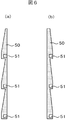
また、図6に導光板50の変形例を示す。図6(a)は、変形例の一つで、図5(a)の導光板の上面図のB−B‘断面図で表しており、LEDを設置する孔51側の厚みを厚くして、LEDから離れるに従い厚みを薄くする構成で、面発光する側を加工する。導光板の下側はフラットでこの下側に反射シートを配置する。また、図6(b)は、(a)とは逆の構成で、導光板の上面をフラットにし、導光板の下側で、LEDを設置する孔51側の厚みを厚くし、LEDから離れるに従い厚みを薄くする構成としている。
FIG. 6 shows a modification of the
次に反射シート40について説明する。図7は反射シート40を示す。反射シート40は、縦方向を3等分し、各々3等分した下部に孔32を設置する。孔32は矩形で、LED基板に搭載されているLED32を挿通させるものである。
Next, the
従って、反射シート40の矩形孔42は、複数のLEDを一定間隔で、横方向の寸法約50cmにおいて、約20個程度設けている。この孔32は、LED基板のLEDに対応している。
Accordingly, the
また、反射シート40には、導光板よりシャーシ10にねじで固定しているため、貫通孔31を各列に3個有している。
In addition, since the
図8は、シャーシ10を示し、図8(a)はその上面図で、図8(b)はシャーシ10の部分断面図である。シャーシ10の大きさは、液晶表示装置が例えば42インチであれば概略横100cm×縦66cmくらいの大きさである。シャーシ10は、一般に鉄板をプレス成形で製造している。また、寸法が概略横100cm×縦66cmくらいの大きさであれば、成形後反りが発生しやすい。そのため、鉄板の板圧を1mm程度と厚めにしたり、図1に示したように、背面より補強材110を設置し、固定している。
FIG. 8 shows the
さらに、シャーシ10に強度を持たせるため、中央の平板の部分には、リブ13を設けている。リブ13は、横長の長円形状としており、内側(バックライト側)に膨らみを持たせた構造としている。そして、図8では縦方向に3列の図を示しているが、3列に限らない。また、シャーシ10は、箱形状として、バックライトユニットを収納する形状とし、周囲はフランジを設けている。
Furthermore, in order to give the
さらに、図8(b)に示すように、シャーシ10のバックライト側に膨らんだリブの間に絶縁板20を設置する。絶縁板20は、シャーシ10と絶縁板20に載置するLED基板との電気接触を防止するとともに、LEDから発生する熱を発散させるようにしている。
Further, as shown in FIG. 8B, an insulating
図8(a)の左下に1か所絶縁板20を設置した場合を示しているが、このようにリブ13のサイドに絶縁板を設置する。このように絶縁板を複数個リブのサイドに設置する。
Although the case where the insulating
また、シャーシ10には、裏面にLED駆動基板を有しており、角穴11を設け、この角穴11を介してバックライトユニットのLED基板と接続している。
Further, the
また、シャーシ10の表面(バックライト側)には導光板を固定するねじ穴130(図2参照)を設置している。ねじ穴は、各2本ずつ4か所に設けている。
A screw hole 130 (see FIG. 2) for fixing the light guide plate is provided on the surface (backlight side) of the
さらに、シャーシ10に表面には、導光板50を位置決めするピン(図示せず)を設け、図5(a)の導光板50の位置決め孔53をシャーシ10に設けたボスに挿入し位置決めする。この位置決めは左右(水平方向)には僅かの自由度は備えているが、上下(垂直方向)には自由度はない。これは導光板とLEDの位置決めを厳しく設定しているためである。
Further, a pin (not shown) for positioning the
図9はシャーシ10の裏面を示す。
FIG. 9 shows the rear surface of the
シャーシ10の裏側には、補強材110を設置固定し、基板を取り付けるボスを設ける。
On the back side of the
シャーシ10の裏側に配置する回路基板は、LED駆動基板11、液晶表示装置全体の電源基板13、液晶パネルを駆動する液晶駆動基板12、メイン基板である信号処理基板14及びHDD装置15がある。HDD装置は必要に応じて外す場合がある。
Circuit boards arranged on the back side of the
このように本実施例では、各LED基板30を一体化せずに別体とし、LEDが格納される各孔51と対応する位置にそれぞれ取り付けている。それは、LEDからの熱により導光板50が膨張した際に、LEDと導光板50の孔51内の入射面との距離が変化しないようにするためである。LEDと入射面との距離が変化すると、LEDからの光の入射効率や導光板50の配光分布が大きく変化し、これが輝度むらの原因となる。これを防止すべく本実施例では、各孔51に対応するLED基板30をそれぞれ取り付けている。このようにすれば、導光板50の熱膨張とともにLED基板30も動くので、LEDの入射面との距離を一定に保つことがで、輝度むらの発生を抑制することができる。
As described above, in this embodiment, the
10‥シャーシ 20‥絶縁シート 30‥LED基板 40‥反射シート
50‥導光板 60‥拡散板 70‥拡散シート 80‥プリズムシート
90‥偏光反射シート 100‥モールドフレーム。
DESCRIPTION OF
Claims (6)
該LED光源からの光を液晶パネル側に導いて出射するための導光板と、
前記LED光源を駆動するための光源基板と、
前記LED光源、前記導光板及び前記LED光源基板が設置されるシャーシとを備え、
前記導光板の前記液晶パネルと対向する光出射面が複数の領域に分割され、その領域毎に映像に応じて光の強度を制御するバックライトユニットを搭載した液晶表示装置において、
前記導光板の大きさを、前記液晶パネルを縦横半分に分割した大きさとしたことを特徴とするバックライトユニットを搭載した液晶表示装置。 An LED light source;
A light guide plate for guiding and emitting light from the LED light source to the liquid crystal panel side;
A light source substrate for driving the LED light source;
A chassis on which the LED light source, the light guide plate and the LED light source substrate are installed;
In the liquid crystal display device equipped with a backlight unit that divides the light emitting surface of the light guide plate facing the liquid crystal panel into a plurality of regions and controls the intensity of light according to the image for each region.
A liquid crystal display device equipped with a backlight unit, wherein the light guide plate has a size obtained by dividing the liquid crystal panel into vertical and horizontal halves.
前記4分割した導光板には、水平方向に3列のLED光源基板を設置することを特徴とするバックライトユニットを搭載した液晶表示装置。 In the liquid crystal display device mounted with the backlight unit according to claim 1,
3. A liquid crystal display device equipped with a backlight unit, wherein the four divided light guide plates are provided with three rows of LED light source substrates in the horizontal direction.
前記4分割した導光板は、フラットであることを特徴とするバックライトユニットを搭載した液晶表示装置。 In the liquid crystal display device mounted with the backlight unit according to claim 1,
The liquid crystal display device mounted with a backlight unit, wherein the light guide plate divided into four is flat.
前記LED光源基板は、複数のLED光源を1列に並べて配置したことを特徴とするバックライトユニットを搭載した液晶表示装置。 In the liquid crystal display device mounted with the backlight unit according to claim 2,
The LED light source substrate is a liquid crystal display device equipped with a backlight unit in which a plurality of LED light sources are arranged in a line.
前記導光板は、表裏の少なくとも一方をパターニングしたことを特徴とするバックライトユニットを搭載した液晶表示装置。 In the liquid crystal display device mounted with the backlight unit according to claim 1,
The light guide plate is a liquid crystal display device equipped with a backlight unit in which at least one of the front and back surfaces is patterned.
前記導光板及び前記LED光源基板との間に反射シートを配置し、
該反射シートの大きさを、導体板とほぼ同じ大きさとしたことを特徴とするバックライトユニットを搭載した液晶表示装置。 In the liquid crystal display device mounted with the backlight unit according to claim 1,
A reflective sheet is disposed between the light guide plate and the LED light source substrate,
A liquid crystal display device mounted with a backlight unit, characterized in that the size of the reflection sheet is substantially the same as that of the conductor plate.
Priority Applications (5)
| Application Number | Priority Date | Filing Date | Title |
|---|---|---|---|
| JP2010270149A JP2012119252A (en) | 2010-12-03 | 2010-12-03 | Liquid crystal display apparatus |
| EP11009000A EP2461192A1 (en) | 2010-12-03 | 2011-11-11 | Liquid crystal display apparatus |
| CN2011103621043A CN102486582A (en) | 2010-12-03 | 2011-11-15 | Liquid crystal display apparatus |
| CN2011204526323U CN202548488U (en) | 2010-12-03 | 2011-11-15 | Liquid crystal display device |
| US13/296,277 US20120140144A1 (en) | 2010-12-03 | 2011-11-15 | Liquid crystal display apparatus |
Applications Claiming Priority (1)
| Application Number | Priority Date | Filing Date | Title |
|---|---|---|---|
| JP2010270149A JP2012119252A (en) | 2010-12-03 | 2010-12-03 | Liquid crystal display apparatus |
Publications (2)
| Publication Number | Publication Date |
|---|---|
| JP2012119252A true JP2012119252A (en) | 2012-06-21 |
| JP2012119252A5 JP2012119252A5 (en) | 2013-01-17 |
Family
ID=45400833
Family Applications (1)
| Application Number | Title | Priority Date | Filing Date |
|---|---|---|---|
| JP2010270149A Pending JP2012119252A (en) | 2010-12-03 | 2010-12-03 | Liquid crystal display apparatus |
Country Status (4)
| Country | Link |
|---|---|
| US (1) | US20120140144A1 (en) |
| EP (1) | EP2461192A1 (en) |
| JP (1) | JP2012119252A (en) |
| CN (2) | CN202548488U (en) |
Cited By (4)
| Publication number | Priority date | Publication date | Assignee | Title |
|---|---|---|---|---|
| JP2016506038A (en) * | 2012-12-18 | 2016-02-25 | コーニンクレッカ フィリップス エヌ ヴェKoninklijke Philips N.V. | Lighting strip, lighting system, panel support element and modular panel system |
| KR20170125657A (en) * | 2016-05-04 | 2017-11-15 | 엘지이노텍 주식회사 | Lighting module and lighting apparatus |
| KR20180024588A (en) * | 2016-08-30 | 2018-03-08 | 엘지이노텍 주식회사 | Lighting module and lighting apparatus |
| JP2019515459A (en) * | 2016-05-04 | 2019-06-06 | エルジー イノテック カンパニー リミテッド | LIGHTING MODULE AND LIGHTING APPARATUS COMPRISING THE SAME |
Families Citing this family (3)
| Publication number | Priority date | Publication date | Assignee | Title |
|---|---|---|---|---|
| US9162613B2 (en) * | 2012-08-29 | 2015-10-20 | Yao Hung Huang | Vehicle rear light assembly |
| JPWO2014141340A1 (en) * | 2013-03-11 | 2017-02-16 | パナソニックIpマネジメント株式会社 | Lighting device and display device |
| JP6554534B2 (en) * | 2015-03-10 | 2019-07-31 | シャープ株式会社 | Lighting device, display device, and television receiver |
Citations (5)
| Publication number | Priority date | Publication date | Assignee | Title |
|---|---|---|---|---|
| JP2006339043A (en) * | 2005-06-02 | 2006-12-14 | Fujifilm Holdings Corp | Planar lighting device, and liquid crystal display device with same |
| JP2006351375A (en) * | 2005-06-16 | 2006-12-28 | Mitsubishi Rayon Co Ltd | Surface light source device |
| JP2007317466A (en) * | 2006-05-25 | 2007-12-06 | Asahi Techno Kk | Surface light emitting device |
| JP2010108601A (en) * | 2008-10-28 | 2010-05-13 | Citizen Electronics Co Ltd | Planar light source and liquid crystal display |
| JP2010177160A (en) * | 2009-02-02 | 2010-08-12 | Enplas Corp | Planar light source device, and display using the same |
Family Cites Families (12)
| Publication number | Priority date | Publication date | Assignee | Title |
|---|---|---|---|---|
| KR20060000544A (en) * | 2004-06-29 | 2006-01-06 | 삼성전자주식회사 | Back light for display device, light source for display device, and light emitting diode using therefor |
| KR100780205B1 (en) * | 2006-04-21 | 2007-11-27 | 삼성전기주식회사 | Backlight unit for liquid crystal display device |
| EP2063171A4 (en) * | 2006-10-27 | 2010-12-01 | Sharp Kk | Light source device, backlight device, and liquid crystal display device |
| WO2009145548A2 (en) * | 2008-05-27 | 2009-12-03 | Lg Electronics Inc. | Led back-light unit and liquid crystal display device using the same |
| JP2010021131A (en) * | 2008-06-09 | 2010-01-28 | Hitachi Ltd | Display device and backlight unit used for the same |
| KR101101134B1 (en) * | 2008-07-03 | 2012-01-05 | 삼성엘이디 주식회사 | Led package and backlight unit having the same |
| TWI539621B (en) * | 2008-07-03 | 2016-06-21 | 三星電子股份有限公司 | Led package and backlight unit having the same |
| KR101287636B1 (en) * | 2008-08-25 | 2013-07-24 | 엘지디스플레이 주식회사 | Backlight unit and liquid crystal display device having the same |
| US8223296B2 (en) * | 2008-08-25 | 2012-07-17 | Lg Display Co. Ltd. | Backlight unit and liquid crystal display device having the same |
| US7905617B2 (en) * | 2008-09-23 | 2011-03-15 | Samsung LED. Co., Ltd. | Backlight unit |
| JP5263593B2 (en) * | 2008-10-07 | 2013-08-14 | ソニー株式会社 | Illumination device and display device |
| JP2010177076A (en) | 2009-01-30 | 2010-08-12 | Hitachi Ltd | Tandem surface light source device, and liquid crystal display device using the same |
-
2010
- 2010-12-03 JP JP2010270149A patent/JP2012119252A/en active Pending
-
2011
- 2011-11-11 EP EP11009000A patent/EP2461192A1/en not_active Withdrawn
- 2011-11-15 CN CN2011204526323U patent/CN202548488U/en not_active Expired - Fee Related
- 2011-11-15 US US13/296,277 patent/US20120140144A1/en not_active Abandoned
- 2011-11-15 CN CN2011103621043A patent/CN102486582A/en active Pending
Patent Citations (5)
| Publication number | Priority date | Publication date | Assignee | Title |
|---|---|---|---|---|
| JP2006339043A (en) * | 2005-06-02 | 2006-12-14 | Fujifilm Holdings Corp | Planar lighting device, and liquid crystal display device with same |
| JP2006351375A (en) * | 2005-06-16 | 2006-12-28 | Mitsubishi Rayon Co Ltd | Surface light source device |
| JP2007317466A (en) * | 2006-05-25 | 2007-12-06 | Asahi Techno Kk | Surface light emitting device |
| JP2010108601A (en) * | 2008-10-28 | 2010-05-13 | Citizen Electronics Co Ltd | Planar light source and liquid crystal display |
| JP2010177160A (en) * | 2009-02-02 | 2010-08-12 | Enplas Corp | Planar light source device, and display using the same |
Cited By (10)
| Publication number | Priority date | Publication date | Assignee | Title |
|---|---|---|---|---|
| JP2016506038A (en) * | 2012-12-18 | 2016-02-25 | コーニンクレッカ フィリップス エヌ ヴェKoninklijke Philips N.V. | Lighting strip, lighting system, panel support element and modular panel system |
| KR20170125657A (en) * | 2016-05-04 | 2017-11-15 | 엘지이노텍 주식회사 | Lighting module and lighting apparatus |
| JP2019515459A (en) * | 2016-05-04 | 2019-06-06 | エルジー イノテック カンパニー リミテッド | LIGHTING MODULE AND LIGHTING APPARATUS COMPRISING THE SAME |
| US11125396B2 (en) | 2016-05-04 | 2021-09-21 | Lg Innotek Co., Ltd. | Light module and lighting device having same |
| JP7126949B2 (en) | 2016-05-04 | 2022-08-29 | エルジー イノテック カンパニー リミテッド | Lighting module and lighting device provided with the same |
| KR102624157B1 (en) * | 2016-05-04 | 2024-01-19 | 엘지이노텍 주식회사 | Lighting module and lighting apparatus |
| KR20180024588A (en) * | 2016-08-30 | 2018-03-08 | 엘지이노텍 주식회사 | Lighting module and lighting apparatus |
| KR102628018B1 (en) * | 2016-08-30 | 2024-01-24 | 엘지이노텍 주식회사 | Lighting module and lighting apparatus |
| KR20240014546A (en) * | 2016-08-30 | 2024-02-01 | 엘지이노텍 주식회사 | Lighting module and lighting apparatus |
| KR102689015B1 (en) * | 2016-08-30 | 2024-07-29 | 엘지이노텍 주식회사 | Lighting module and lighting apparatus |
Also Published As
| Publication number | Publication date |
|---|---|
| CN202548488U (en) | 2012-11-21 |
| CN102486582A (en) | 2012-06-06 |
| US20120140144A1 (en) | 2012-06-07 |
| EP2461192A1 (en) | 2012-06-06 |
Similar Documents
| Publication | Publication Date | Title |
|---|---|---|
| TWI418898B (en) | Backlight unit and liquid crystal display using the same | |
| US8436957B2 (en) | Liquid crystal display device having good heat radiating function | |
| JP5509154B2 (en) | Light emitting device and display device | |
| JP2012118440A (en) | Liquid crystal display apparatus | |
| KR101343390B1 (en) | Backlight Unit Including Diffusing Plate and Liquid Crystal Display Device Using The Same | |
| KR100999780B1 (en) | Optical assembly, backlight unit having the same, and display apparatus thereof | |
| JP2012119252A (en) | Liquid crystal display apparatus | |
| KR20110003777A (en) | Optical assembly, backlight unit having the same, and display apparatus thereof | |
| KR20110097086A (en) | Backlight assembly and display apparatus having the same | |
| KR101020923B1 (en) | Optical assembly, backlight unit having the same, and display apparatus thereof | |
| JP7108484B2 (en) | display device and television receiver | |
| KR101028294B1 (en) | Optical assembly, backlight unit having the same, and display apparatus thereof | |
| KR101413140B1 (en) | Light diffusion plate having non-uniform local microlens array pattern and liquid crystal display device comprising the same | |
| KR20080036437A (en) | Backlight assembly and liquid crystal display comprising the same | |
| KR101296456B1 (en) | Back light Unit and Liquid Crystal Display using the same | |
| KR102002458B1 (en) | Liquid crystal display device | |
| JP5392930B2 (en) | Planar light source and liquid crystal display device | |
| KR101042698B1 (en) | Surface light source apparatus | |
| KR102066089B1 (en) | Back light unit and method for assembling the same | |
| KR101064088B1 (en) | Backlight unit and display device with optical assembly | |
| KR101658145B1 (en) | Back light unit and method for assembling the same | |
| KR101047704B1 (en) | Backlight unit and display device with optical assembly | |
| KR20120135652A (en) | Liquid crystal display device | |
| JP4517307B2 (en) | Surface light source device and image display device | |
| KR101072052B1 (en) | optical assembly, backlight unit having the same, and display apparatus thereof |
Legal Events
| Date | Code | Title | Description |
|---|---|---|---|
| A521 | Written amendment |
Free format text: JAPANESE INTERMEDIATE CODE: A523 Effective date: 20121122 |
|
| A621 | Written request for application examination |
Free format text: JAPANESE INTERMEDIATE CODE: A621 Effective date: 20121122 |
|
| A977 | Report on retrieval |
Free format text: JAPANESE INTERMEDIATE CODE: A971007 Effective date: 20130405 |
|
| A131 | Notification of reasons for refusal |
Free format text: JAPANESE INTERMEDIATE CODE: A131 Effective date: 20130416 |
|
| A02 | Decision of refusal |
Free format text: JAPANESE INTERMEDIATE CODE: A02 Effective date: 20130820 |