WO2016143616A1 - 光源、光源を含む装置、及び光源の製造方法 - Google Patents
光源、光源を含む装置、及び光源の製造方法 Download PDFInfo
- Publication number
- WO2016143616A1 WO2016143616A1 PCT/JP2016/056326 JP2016056326W WO2016143616A1 WO 2016143616 A1 WO2016143616 A1 WO 2016143616A1 JP 2016056326 W JP2016056326 W JP 2016056326W WO 2016143616 A1 WO2016143616 A1 WO 2016143616A1
- Authority
- WO
- WIPO (PCT)
- Prior art keywords
- white pigment
- light source
- pigment particles
- particles
- emitting element
- Prior art date
- Legal status (The legal status is an assumption and is not a legal conclusion. Google has not performed a legal analysis and makes no representation as to the accuracy of the status listed.)
- Ceased
Links
Images



Classifications
-
- H—ELECTRICITY
- H10—SEMICONDUCTOR DEVICES; ELECTRIC SOLID-STATE DEVICES NOT OTHERWISE PROVIDED FOR
- H10H—INORGANIC LIGHT-EMITTING SEMICONDUCTOR DEVICES HAVING POTENTIAL BARRIERS
- H10H20/00—Individual inorganic light-emitting semiconductor devices having potential barriers, e.g. light-emitting diodes [LED]
- H10H20/80—Constructional details
- H10H20/85—Packages
- H10H20/851—Wavelength conversion means
-
- H—ELECTRICITY
- H10—SEMICONDUCTOR DEVICES; ELECTRIC SOLID-STATE DEVICES NOT OTHERWISE PROVIDED FOR
- H10H—INORGANIC LIGHT-EMITTING SEMICONDUCTOR DEVICES HAVING POTENTIAL BARRIERS
- H10H20/00—Individual inorganic light-emitting semiconductor devices having potential barriers, e.g. light-emitting diodes [LED]
- H10H20/80—Constructional details
- H10H20/85—Packages
- H10H20/852—Encapsulations
- H10H20/854—Encapsulations characterised by their material, e.g. epoxy or silicone resins
Definitions
- the present invention relates to the structure and manufacturing method of a light source.
- the present invention relates to an apparatus including a light source.
- the device including the light source is, for example, an indoor lighting system, an outdoor lighting system, a lighting device inside or outside a vehicle, and a portable electronic device.
- a light source having a light emitting element and a sealing resin that contains phosphor particles and seals the light emitting element is known.
- the sealing resin that includes the phosphor particles and seals the light emitting element may be transparent.
- the sealing resin that includes the phosphor particles and seals the light emitting element may be a light-transmitting sealing resin.
- a light source that emits white light is known.
- a light emitting element there are a blue light emitting diode element (blue LED element) and a light source including phosphor particles and having a sealing resin for sealing the blue LED element.
- the phosphor particles of the light source include yttrium / aluminum / garnet phosphor (YAG phosphor) particles.
- the sealing resin containing YAG phosphor particles appears yellow as the color of the YAG phosphor particles when the blue LED element is not emitting light.
- the sealing resin containing the YAG phosphor particles may be seen from the outside of the luminaire.
- the color of the phosphor particles contained in the light source may affect the appearance of the device containing the light source.
- a light source having a light emitting element and a light transmissive member including phosphor particles disposed above the light emitting element has been disclosed. Even when not used as a light source, a light emitting device has been proposed in which a standby current is supplied to a light emitting element to cause the light emitting element to emit light slightly (Patent Document 1).
- a light-emitting device having a light-emitting element, a phosphor plate disposed on the light-emitting element, and a diffusion plate disposed on the phosphor plate has been proposed (Patent Document 2).
- a light-emitting diode having a light-emitting element, a reflecting mirror having a high-reflectivity reflecting surface disposed above the light-emitting surface of the light-emitting element, and a phosphor layer applied to one surface of the reflecting mirror has been proposed (patent) Reference 3).
- a light emitting device having a blue light emitting element and a phosphor unit has been proposed.
- the phosphor unit has a pair of substrates and a phosphor dispersion layer disposed between the pair of substrates.
- the pair of substrates may have a wavelength filter. Further, the pair of substrates may have a prism surface (Patent Document 4).
- One embodiment according to the present invention provides a light source having a structure in which the color of the phosphor particles is inconspicuous. Moreover, one of the embodiments according to the present invention provides an apparatus including a light source having a structure in which the color of the phosphor particles is inconspicuous. Furthermore, one of the embodiments according to the present invention presents a method of manufacturing a light source having a structure in which the color of the phosphor particles is not noticeable.
- the light source includes a light emitting element and a sealing resin that includes phosphor particles and white pigment particles to seal the light emitting element.
- the phosphor particles are located closer to the light emitting element than the white pigment particles.
- the light source may further include a substrate on which the light emitting element is electrically mounted. It is disclosed that a light-emitting element mounted on a substrate is sealed on the substrate by a sealing resin including phosphor particles and white pigment particles.
- the white pigment particles can have a ratio in the range of 0.5% to 1% of the total amount of the sealing resin including the phosphor particles and the white pigment particles.
- white pigment particles of a sealing resin including phosphor particles and white pigment particles are included in the sealing resin in the form of a layer.
- the layer of white pigment particles is located on at least a part of the outer surface of the sealing resin.
- the layer of white pigment particles has a thickness of at least 0.0025 mm.
- the layer of white pigment particles has a thickness in the range of 0.0025 mm to 0.005 mm.
- the layer of white pigment particles is in a position covering the light emitting surface of the light emitting element from above.
- the sealing resin containing the phosphor particles and the white pigment particles contains a silicone resin.
- the phosphor particles contained in the sealing resin contain yttrium, aluminum, and garnet.
- the white pigment particles contained in the sealing resin contain titanium oxide.
- the sealing resin is a cured silicone resin.
- the ratio of white pigment particles is 0.5% to 1% of the total amount of the silicone resin including phosphor particles and white pigment particles.
- the apparatus has a light source according to an embodiment of the present invention and a transparent cover that covers the light source.
- a light source manufacturing method includes electrically mounting a light emitting element on a substrate; the proportion of white pigment particles is the total amount of silicone resin containing phosphor particles and white pigment particles. Mixing phosphor particles and white pigment particles in a liquid silicone resin so that the ratio is 0.5% to 1%; a liquid silicone resin in which phosphor particles and white pigment particles are mixed.
- the white pigment particles are formed in a layer having a thickness of 0.025 mm or more and 0.005 mm or less in the silicone resin.
- FIG. 1 illustrates an embodiment of an apparatus including a light source according to an embodiment of the present invention.
- titanium oxide used as the white pigment
- the relationship between the concentration of titanium oxide contained in the sealing resin and the amount of light (lm) from the light-emitting element that passes through the white pigment particle layer is shown.
- titanium oxide used as the white pigment
- the relationship between the concentration of titanium oxide contained in the sealing resin and the light transmittance from the light emitting element that transmits the white pigment particle layer is shown.
- 2 shows a part of a manufacturing process of a light source according to an embodiment of the present invention.
- FIG. 6A is a schematic explanatory diagram illustrating a state where phosphor particles and white pigment particles are mixed in the sealing resin before the sealing resin is cured. 2 shows a part of a manufacturing process of a light source according to an embodiment of the present invention.
- FIG. 6B is a schematic explanatory diagram showing a state where phosphor particles are precipitated and white pigment particles are starting to move upward in the sealing resin.
- relative terms such as “below”, “above”, “above”, and “below” are distinct from certain elements, regions or portions shown in the figures. It may be used as a depiction of the relationship to an element, region or part of Of course, these terms are intended to include different orientations of the light source or device in addition to the orientation shown in the figures.
- FIG. 1 shows a top view of a light source according to an embodiment of the present invention.
- 2 shows a II-II cross-sectional view of the light source according to the embodiment of the present invention shown in FIG.
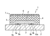
- the cross-sectional view of FIG. 2 illustrates the positional relationship between the phosphor particles 5 and the white pigment particles 6 in the sealing resin 4.
- the light source 1 includes a light emitting element 3, phosphor particles 5 and white pigment particles 6, and includes a sealing resin 4 that seals the light emitting element 3.
- the phosphor particles 5 are located closer to the light emitting element 3 than the white pigment particles 6.
- the first element electrode 3a of the light emitting element 3 is electrically connected to the first electrode pattern 9a of the substrate 2 via the bump 8a.
- the second element electrode 3b of the light emitting element 1 is electrically connected to the second electrode pattern 10a of the substrate 2 via the bumps 8b.
- the first electrode pattern 9 a of the substrate 2 is electrically connected to the first electrode 9.
- the second electrode pattern 10 a of the substrate 2 is electrically connected to the second electrode 10.
- a current can be supplied to the light source 1 from an external power source via the first electrode 9 and the second electrode 10 of the substrate 2.
- the electrode pattern and electrode arrangement and design can be freely selected by those skilled in the art.
- the light emitting element 3 can be electrically connected to the first electrode pattern 9a and the second electrode pattern 10a of the substrate 2 via metal wires instead of the bumps 8a and 8b. is there.
- the first element electrode 3 a and the second element electrode 3 b are located on the upper surface of the light emitting element 3.
- the number of the light emitting elements 3 may be one or plural.
- the plurality of light emitting elements 3 may be electrically connected in series and / or in parallel.
- the phosphor particles 5 included in the sealing resin 4 include, for example, yttrium / aluminum / garnet phosphor (YAG phosphor) particles.
- the sealing resin 4 containing YAG phosphor particles appears yellow as the color of the YAG phosphor particles when the blue LED element is not emitting light.
- the sealing resin 4 containing YAG phosphor particles may be seen from the outside of the lighting fixture.
- the phosphor particles are not limited to YAG phosphor particles.
- the phosphor particles can have various colors. When the color of the phosphor particles is visible from the outside, the appearance of the light source including the phosphor particles and / or the appearance of the device including the light source may be affected.
- the white pigment particles 6 in the sealing resin 4 including the phosphor particles 5 and the white pigment particles 6 form a layer 7 of the white pigment particles 6.
- the phosphor particles 5 and the white pigment particles 6 are contained in the sealing resin 4.
- a light source having a structure in which a white pigment plate is separately bonded onto a resin containing phosphor particles may have a separate adhesive layer or air layer interposed therebetween.
- the layer 7 of the white pigment particles 6 is difficult to separate from the sealing resin 4.
- the layer 7 of white pigment particles 6 is located on at least a part of the outer surface of the sealing resin 4. In the present embodiment, the layer 7 of the white pigment particles 6 is in a position that covers the light emitting surface 3 ′ of the light emitting element 3 from above.
- the light source 1 in which the layer 7 of the white pigment particles 6 has a thickness in the range of 0.0025 mm to 0.005 mm was able to ensure 70% or more of the light transmittance. Further, when the light source 1 in which the layer 7 of the white pigment particles 6 had a thickness in the range of 0.0025 mm or more and 0.005 mm or less was turned off, the light source 1 could show the color of the phosphor particles 5 inconspicuously.
- FIG. 3 shows an embodiment of an apparatus including a light source according to an embodiment of the present invention.
- FIG. 3 shows a light bulb as an example of an apparatus including the light source 1.
- the device 100 including the light source 1 has a cover 11.
- the cover 11 is transparent.
- transparent cover includes a cover having such a transparency that the outline of the sealing resin 4 can be seen through the cover.
- the light bulb which is the device 100 of the present embodiment, has a holder 12 on which the light source 1 is mounted, and a base 13 below the holder 12.
- the first terminal 13 a and the second terminal 13 b of the base 13 are electrically connected to the first electrode 9 and the second electrode 10 of the substrate 2 of the light source 1.
- the base 13 is shown as a screw-type base in this embodiment, those skilled in the art can freely select the shape of the base 13.
- the “apparatus” including the light source according to the embodiment of the present invention is not limited to the light bulb shown in FIG.
- the term “apparatus” here includes an apparatus in which a light source can be visually recognized from the outside. Therefore, the “device” may be, for example, an indoor lighting system including a downlight, an outdoor lighting system, a lighting device inside or outside a vehicle, or a portable electronic device.
- the structure of the light source 1 according to the embodiment of the present invention does not make the color of the phosphor particles 5 included in the sealing resin 4 stand out. Therefore, the influence of the color of the phosphor particles 5 on the appearance of the device 100 including the light source 1 can be suppressed.
- FIG. 4 shows the concentration of titanium oxide contained in the sealing resin 4 and the amount of light (lm) from the light emitting element 3 that passes through the layer 7 of white pigment particles 6 when titanium oxide is used as the white pigment. The relationship is shown. Note that the amount (lm) of light flux from the light-emitting element 3 when the concentration of titanium oxide contained in the sealing resin 4 is 0% varies depending on the number and luminance of the light-emitting elements 3.
- FIG. 5 shows the relationship between the concentration of titanium oxide contained in the sealing resin 4 and the transmittance of light from the light emitting element 3 that passes through the layer 7 of white pigment particles 6 when titanium oxide is used as the white pigment. Indicates.
- the proportion of titanium oxide is 1% of the total amount of the silicone resin containing titanium oxide which is the phosphor particles 5 and the white pigment particles 6, the color of the phosphor particles 5 contained in the sealing resin 4 of the light source 1 is Compared to 0.5%, the light source 1 became less noticeable when the light source 1 was not turned on.
- the proportion of titanium oxide is 1% of the total amount of the silicone resin containing the phosphor particles 5 and the white pigment particles 6 including the titanium oxide, the light flux transmitted through the layer 7 of the white pigment particles 6 of the sealing resin 4 The transmittance was about 75%.
- the proportion of titanium oxide is 0.5% to 1% of the total amount of the phosphor particles 5 and the silicone resin containing titanium oxide which is the white pigment particles 6, the light transmittance of the layer 7 of the white pigment particles 6 While ensuring 70% or more, the color of the phosphor particles 5 could be made inconspicuous.
- the method of manufacturing the light source 1 is to electrically mount the light emitting element 3 on the substrate 2; the ratio of the white pigment particles 6 to the phosphor particles 5 and the white pigment particles 6; Mixing phosphor particles 5 and white pigment particles 6 in a liquid silicone resin so that the ratio is 0.5% to 1% of the total amount of silicone resin contained; mixing phosphor particles 5 and white pigment particles 6 Sealing the light-emitting element 3 electrically mounted on the substrate 2 with a liquid silicone resin; white pigment particles 6 in the liquid silicone resin so that the phosphor particles 5 cover the light-emitting element 3.
- the heavier phosphor particles 5 are precipitated; the phosphor particles 5 heavier than the white pigment particles 6 are precipitated and arranged at a position close to the light emitting element 3, and the outer surface of the cured silicone resin. Firefly so that it is close to Curing the liquid silicone resin in which the light body particles 5 and the white pigment particles 6 are mixed.
- FIG. 6A and 6B show a part of the manufacturing process of the light source 1 according to the embodiment of the present invention.
- FIG. 6A is a schematic explanatory view showing a state where phosphor particles 5 and white pigment particles 6 are mixed in the sealing resin 4 before the sealing resin 4 is cured.
- FIG. 6B is a schematic explanatory diagram showing a state in which the phosphor particles 5 are precipitated and the white pigment particles 6 are starting to move upward in the sealing resin 4.
- the viscosity of the sealing resin 4 can be adjusted.
- the white pigment particles 6 lighter than the phosphor particles 5 are deposited on the phosphor particles 5 on which the white pigment particles 6 are precipitated before and / or during the curing of the sealing resin 4. As formed, the viscosity of the sealing resin 4 can be set.
- the white pigment particles 6 are formed in the layer 7 having a thickness of 0.025 mm or more and 0.005 mm or less in the silicone resin.
- the sealing resin 4 may contain particles having other effects in addition to the phosphor particles 5 and the white pigment particles 6.
- the sealing resin 4 may include particles having a diffusion effect and / or particles that transmit a specific wavelength.
- the phosphor particles 5 and the white pigment particles 6 are included in the sealing resin 4. Therefore, another member can be provided on the sealing resin 4.
- a diffusion plate and / or a specific wavelength transmission filter may be provided on the sealing resin 4.
Landscapes
- Led Device Packages (AREA)
Abstract
【課題】 本発明に係る実施形態の1つは、課題の一つとして、蛍光体粒子の色が目立たない構造の光源を提供する。 【解決手段】 発光素子(3)と、蛍光体粒子(5)と白色顔料粒子(6)を含み、発光素子(3)を封止する封止樹脂(4)と、を有し、発光素子(3)を封止する封止樹脂(4)内において、蛍光体粒子(5)は白色顔料粒子(6)よりも発光素子(3)に近い位置にある、光源(1)。
Description
本発明は、光源の構造と製法に関する。本発明は、光源を含む装置に関する。光源を含む装置は、例えば、室内照明システム、屋外照明システム、乗り物の車内外の照明装置、及び携帯電子機器である。
発光素子と、蛍光体粒子を含み発光素子を封止する封止樹脂を有する光源が知られている。蛍光体粒子を含み発光素子を封止する封止樹脂は、透明であっても良い。蛍光体粒子を含み発光素子を封止する封止樹脂は光透過性の封止樹脂であっても良い。発光素子に電流が流れると、発光素子が光を出す。蛍光体粒子は、発光素子の光によって励起されて、光を出す。発光素子に電流が流れると、発光素子を封止し蛍光体粒子を含む封止樹脂全体が、発光して見える。
例えば、白色に見える光を出す光源が知られている。発光素子として青色発光ダイオード素子(青色LED素子)と、蛍光体粒子を含み、青色LED素子を封止する封止樹脂を有する光源がある。この光源の蛍光体粒子は、イットリウム・アルミニウム・ガーネット蛍光体(YAG蛍光体)粒子を含む。YAG蛍光体粒子を含む封止樹脂は、青色LED素子が発光していない時、YAG蛍光体粒子の色である黄色に見える。光源が照明器具内に実装されると、照明器具の外側から、YAG蛍光体粒子を含む封止樹脂が見える場合がある。光源に含まれる蛍光体粒子の色が、その光源を含む装置の外観に影響を与えることがある。
発光素子と、発光素子の上方に配置した、蛍光体粒子を含む光透過部材を有する光源が開示された。光源として使用しない場合でも、発光素子に待機電流を流して発光素子をわずかに発光させる発光装置が提案された(特許文献1)。
発光素子と、発光素子の上に配置された蛍光体板と、蛍光体板の上に配置された拡散板を有する発光装置が提案された(特許文献2)。
発光素子と、発光素子の発光面の上方に配置された高反射率の反射面を有する反射鏡と、反射鏡の一面に塗布された蛍光体層と、を有する発光ダイオードが提案された(特許文献3)。
青色発光素子と、蛍光体ユニットを有する発光装置が提案された。蛍光体ユニットは、一対の基板と、一対の基板の間に配置された蛍光体分散層を有する。一対の基板は、波長フィルタを有していても良い。また、一対の基板は、プリズム面を有していても良い(特許文献4)。
本発明に係る実施形態の1つは、蛍光体粒子の色が目立たない構造の光源を提供する。また、本発明に係る実施形態の1つは、蛍光体粒子の色が目立たない構造の光源を含む装置を提供する。さらに、本発明に係る実施形態の1つは、蛍光体粒子の色が目立たない構造を持つ光源の製法を提示する。
本発明の第1の態様として、光源は、発光素子と、蛍光体粒子と白色顔料粒子を含み発光素子を封止する封止樹脂を有する。発光素子を封止する封止樹脂内において、蛍光体粒子は、白色顔料粒子よりも発光素子に近い位置にある。
光源は、さらに、発光素子が電気的に実装される基板を有していても良い。基板上に実装された発光素子は、蛍光体粒子と白色顔料粒子を含む封止樹脂によって、基板上において封止されることが開示される。
白色顔料粒子は、蛍光体粒子と白色顔料粒子を含む封止樹脂の全体量の、0.5%から1%の範囲にある割合とすることが出来る。
蛍光体粒子と白色顔料粒子を含む封止樹脂の白色顔料粒子は、層の形状で、封止樹脂に含まれていることが、開示される。
白色顔料粒子の層は、封止樹脂の外表面の少なくとも一部に位置することが、開示される。
白色顔料粒子の層は、少なくとも0.0025mmの厚みを有することが、開示される。
白色顔料粒子の層は、0.0025mm以上0.005mm以下の範囲の厚みを有することが、開示される。
白色顔料粒子の層は、発光素子の発光面を上方から覆う位置にあることが、開示される。
蛍光体粒子と白色顔料粒子を含む封止樹脂は、シリコーン樹脂を含むことが、開示される。
本発明の光源の実施形態の1つとして、封止樹脂に含まれる蛍光体粒子は、イットリウム、アルミニウム、ガーネットを含んでいることが、開示される。
封止樹脂に含まれる白色顔料粒子は、酸化チタンを含むことが、開示される。
封止樹脂は、硬化(cure)されたシリコーン樹脂であることが、開示される。
白色顔料粒子の割合は、蛍光体粒子と白色顔料粒子を含むシリコーン樹脂の全体量の0.5%から1%であることが、開示される。
本発明の第2の態様として、装置は、本発明の実施形態に係る光源と、光源を覆う透明なカバーを有することが、開示される。
本発明の第3の態様として、光源の製造方法は、発光素子を基板上に電気的に実装すること;白色顔料粒子の割合を、蛍光体粒子と白色顔料粒子を含むシリコーン樹脂の全体量の0.5%から1%の割合にするように、液状のシリコーン樹脂に蛍光体粒子と白色顔料粒子を混合させること;蛍光体粒子と白色顔料粒子を混合させた液状のシリコーン樹脂で、基板上に電気的に実装された発光素子を封止すること;蛍光体粒子が発光素子を覆うように、液状のシリコーン樹脂内において、白色顔料粒子よりも重い蛍光体粒子を沈殿させること;白色顔料粒子よりも重い蛍光体粒子を沈殿させて発光素子に近い位置に配置し、白色顔料粒子を硬化されたシリコーン樹脂の外表面に近い位置になるように蛍光体粒子と白色顔料粒子が混合された液状のシリコーン樹脂を硬化させること、を有することが、開示される。
白色顔料粒子が、シリコーン樹脂の中で、0.025mm以上0.005mm以下の厚みの層に形成されることが、本発明の製造方法の実施形態において開示される。
本発明の実施形態は、実施形態の示される添付の図面を参照して、以下により詳細に説明する。しかしながら、本発明は、多くの異なる形態において実施されることが可能である。したがって、ここに記載される実施形態に限定されるものとして解釈されるべきではない。本発明の実施形態は、本開示を詳細で完全なものとし、本発明の範囲を当業者に詳細に伝えるために提示される。
本明細書に使用されるように、「および/もしくは」という言葉は、関連して記載された項目の一つ、もしくは一つ以上の組み合わせのうちのいずれか、それらの組み合わせの全て、を含んでいる。
本明細書で用いられる「~の下の」や「~の上の」、「上方の」や「下方の」のような相対語は、図に示される、ある要素、領域もしくは部分と、別の要素、領域もしくは部分との関係を描写するものとして使用されている場合がある。当然ながら、これらの言葉は、図に示される方向に加えて、光源や装置の異なる向きを含むことを意図されている。
図1は、本発明の実施形態に係る光源の上面図を示す。図2は、図1で示される本発明の実施形態に係る光源のII-II断面図を示す。図2の断面図は、封止樹脂4内での蛍光体粒子5と白色顔料粒子6の位置関係を示す説明的に示す。光源1は、発光素子3と、蛍光体粒子5と白色顔料粒子6を含み、発光素子3を封止する封止樹脂4を有する。発光素子3を封止する封止樹脂4内において、蛍光体粒子5は白色顔料粒子6よりも発光素子3に近い位置にある。
図1で示す発光素子3は、発光素子3の下面に第1素子電極3aと第2素子電極3bを有する。発光素子3の第1素子電極3aは、バンプ8aを介して、基板2の第1電極パターン9aに電気的に接続される。発光素子1の第2素子電極3bは、バンプ8bを介して、基板2の第2電極パターン10aに電気的に接続される。基板2の第1電極パターン9aは、第1電極9に電気的に接続される。基板2の第2電極パターン10aは、第2電極10に電気的に接続される。基板2の第1電極9と第2電極10を介して、外部の電源から光源1に電流の供給が可能である。電極パターンや電極の配置やデザインについては、当業者によって自由に選択可能である。また、図1では、発光素子3は、バンプ8a,8bの代わりに、金属ワイヤーを介して、基板2の第1電極パターン9aと第2電極パターン10aに電気的に接続されることも可能である。この場合には、発光素子3の上面に第1素子電極3aと第2素子電極3bが位置する。
発光素子3の数は、一つでも良いし、複数設けても良い。複数の発光素子を封止樹脂4内に配置する場合、複数の発光素子3は、互いに電気的に直列接続および/もしくは並列接続されていても良い。
本発明の光源1の実施形態の1つとして、封止樹脂4に含まれる蛍光体粒子5は、例えば、イットリウム・アルミニウム・ガーネット蛍光体(YAG蛍光体)粒子を含む。YAG蛍光体粒子を含む封止樹脂4は、青色LED素子が発光していない時、YAG蛍光体粒子の色である黄色に見える。光源1が照明器具内に実装されると、照明器具の外側から、YAG蛍光体粒子を含む封止樹脂4が見える場合がある。なお、蛍光体粒子は、YAG蛍光体粒子に限定されるものではない。蛍光体粒子は、様々な色味を持つ可能性がある。蛍光体粒子の色味を外側から視認可能である場合、その蛍光体粒子を含む光源の外観および/もしくは光源を含む装置の外観に影響を与えることがある。
図2で示すように、蛍光体粒子5と白色顔料粒子6を含む封止樹脂4内の白色顔料粒子6は、白色顔料粒子6の層7を形成している。蛍光体粒子5と白色顔料粒子6は、封止樹脂4内に含まれている。蛍光体粒子が含まれる樹脂の上に白色顔料板を別個に接着する構造を持つ光源は、別個に接着層や空気層を介在する場合がある。本発明の実施形態に係る光源1では、別個の接着層や空気層は介在しないので、白色顔料粒子6の層7が封止樹脂4から分離しにくい。
白色顔料粒子6の層7は、封止樹脂4の外表面の少なくとも一部に位置する。本実施形態では、白色顔料粒子6の層7は、発光素子3の発光面3’を上方から覆う位置にある。
白色顔料粒子6の層7が、0.0025mm以上0.005mm以下の範囲の厚みを有する光源1は、光の透過率の70%以上を確保することが出来た。また、白色顔料粒子6の層7が、0.0025mm以上0.005mm以下の範囲の厚みを有する光源1の消灯時に、光源1は、蛍光体粒子5の色を目立たなく見せることが出来た。
図3は、本発明の実施形態に係る光源を含む装置の実施形態を示す。図3は、光源1を含む装置の一例として、電球を示す。光源1を含む装置100は、カバー11を有する。カバー11は透明である。ここで「透明なカバー」という言葉は、カバーを通して封止樹脂4の輪郭が見える程度の透明度を有するカバーも含む。
本実施形態の装置100である電球は、光源1が実装されるホルダ12と、ホルダ12の下方にベース13を有している。ベース13の第1端子13aと第2端子13bは、光源1の基板2の第1電極9と第2電極10に電気的に接続されている。ベース13は、本実施形態では、ねじ込み式の口金として示されているが、当業者はベース13の形状を自由に選択できる。
なお、本発明の実施形態に係る光源を含む「装置」は、図3で示される電球に限定されるものではない。ここでの「装置」という言葉は、外側から光源が視認出来る装置を含む。したがって、「装置」は、例えば、ダウンライトを含む室内照明システム、屋外照明システム、乗り物の車内外の照明装置、もしくは携帯電子機器であっても良い。本発明の実施形態に係る光源1の構造は、封止樹脂4に含まれる蛍光体粒子5の色を目立たせない。したがって、蛍光体粒子5の色味が、光源1を含む装置100の外観に与える影響を抑制出来る。
図4は、白色顔料として酸化チタンを使用した場合に、封止樹脂4に含まれる酸化チタンの濃度と、白色顔料粒子6の層7を透過する発光素子3からの光束の量(lm)との関係を示す。なお、封止樹脂4に含まれる酸化チタンの濃度が0%の時の発光素子3からの光束の量(lm)は、発光素子3の数や輝度によって異なる。図5は、白色顔料として酸化チタンを使用した場合に、封止樹脂4に含まれる酸化チタンの濃度と、白色顔料粒子6の層7を透過する発光素子3からの光の透過率との関係を示す。
酸化チタンの割合が、蛍光体粒子5と白色顔料粒子6である酸化チタンを含むシリコーン樹脂の全体量の0.5%の時、光源1の封止樹脂4に含まれる蛍光体粒子5の色は、光源1の非点灯時の目視で目立たなくなった。酸化チタンの割合が、蛍光体粒子5と白色顔料粒子6である酸化チタンを含むシリコーン樹脂の全体量の0.5%の時、封止樹脂4の白色顔料粒子6の層7を透過する光束光の透過率は約85%となった。
酸化チタンの割合が、蛍光体粒子5と白色顔料粒子6である酸化チタンを含むシリコーン樹脂の全体量の1%の時、光源1の封止樹脂4に含まれる蛍光体粒子5の色は、0.5%の時と比べて、光源1の非点灯時の目視で、さらに目立たなくなった。酸化チタンの割合が、蛍光体粒子5と白色顔料粒子6である酸化チタンを含むシリコーン樹脂の全体量の1%の時、封止樹脂4の白色顔料粒子6の層7を透過する光束光の透過率は約75%となった。
酸化チタンの割合が、蛍光体粒子5と、白色顔料粒子6である酸化チタンを含むシリコーン樹脂の全体量の0.5%から1%であれば、白色顔料粒子6の層7の光の透過率の70%以上を確保しながら、蛍光体粒子5の色を目立たなくすることが出来た。
本発明の実施形態の1つに係る光源1の製造方法は、発光素子3を基板2上に電気的に実装すること;白色顔料粒子6の割合を、蛍光体粒子5と白色顔料粒子6を含むシリコーン樹脂の全体量の0.5%から1%の割合にするように、液状のシリコーン樹脂に蛍光体粒子5と白色顔料粒子6を混合させること;蛍光体粒子5と白色顔料粒子6を混合させた液状のシリコーン樹脂で、基板2上に電気的に実装された発光素子3を封止すること;蛍光体粒子5が発光素子3を覆うように、液状のシリコーン樹脂内において、白色顔料粒子6よりも重い蛍光体粒子5を沈殿させること;白色顔料粒子6よりも重い蛍光体粒子5を沈殿させて発光素子3に近い位置に配置し、白色顔料粒子6を硬化されたシリコーン樹脂の外表面に近い位置になるように蛍光体粒子5と白色顔料粒子6が混合された液状のシリコーン樹脂を硬化させること、を有する。
図6A及び図6Bは、本発明の実施形態に係る光源1の製造過程の一部を示す。図6Aは、封止樹脂4の硬化前に、蛍光体粒子5と白色顔料粒子6が封止樹脂4内で混在している状態を示す概略説明図である。図6Bは、封止樹脂4内で、蛍光体粒子5が沈殿し、白色顔料粒子6が上方へ移動し始めている状態を示す概略説明図である。封止樹脂4の粘度は、調整可能である。本発明の光源1に係る実施形態では、封止樹脂4の硬化前および/もしくは硬化中に、蛍光体粒子5よりも軽い白色顔料粒子6が、沈殿する蛍光体粒子5の上に層7を形成するように、封止樹脂4の粘度を設定することが出来る。
白色顔料粒子6は、シリコーン樹脂の中で、0.025mm以上0.005mm以下の厚みの層7に形成される。
封止樹脂4は、蛍光体粒子5と白色顔料粒子6に加えて、別の効果を有する粒子を含んでいても良い。封止樹脂4は、拡散効果を有する粒子および/もしくは特定の波長を透過する粒子を含んでいても良い。
本発明の実施形態に係る光源1において、蛍光体粒子5と白色顔料粒子6は、封止樹脂4内に含まれている。したがって、封止樹脂4の上に別の部材を設けることが可能である。例えば、拡散板および/もしくは特定の波長透過フィルタを封止樹脂4上に設けても良い。
本発明の主題の教示から離れることなく、様々な構成要素の組み合わせが他にも可能である。したがって、本発明の主題はここに記載されて図面に図示された例示的実施形態に限定されるものとして解釈されるべきではなく、記載された様々な実施形態の要素の組み合わせを包含するものでもある。
Claims (16)
- 発光素子と、
蛍光体粒子と白色顔料粒子を含み、発光素子を封止する封止樹脂を有し、
発光素子を封止する封止樹脂内において、蛍光体粒子は、白色顔料粒子よりも発光素子に近い位置にある、光源。 - さらに、発光素子が電気的に実装される基板を有し、
基板上に実装された発光素子は、蛍光体粒子と白色顔料粒子を含む封止樹脂によって、基板上において封止される、請求項1の光源。 - 白色顔料粒子は、蛍光体粒子と白色顔料粒子を含む封止樹脂の全体量の、0.5%から1%の範囲の割合である、請求項1又は請求項2に記載の光源。
- 蛍光体粒子と白色顔料粒子を含む封止樹脂の白色顔料粒子は、層の形状で封止樹脂の中に含まれる、請求項1から請求項3のいずれか一つに記載の光源。
- 白色顔料粒子の層は、封止樹脂の外表面の少なくとも一部に位置する、請求項4に記載の光源。
- 白色顔料粒子の層は、少なくとも0.0025mmの厚みを有する、請求項4又は請求項5に記載の光源。
- 白色顔料粒子の層は、0.0025mm以上0.005mm以下の範囲の厚みを有する、請求項4又は請求項5に記載の光源。
- 白色顔料粒子の層は、発光素子の発光面を上方から覆う位置にある、請求項4から請求項7のいずれかに記載の光源。
- 蛍光体粒子と白色顔料粒子を含む封止樹脂は、シリコーン樹脂を含む、請求項1から請求項8のいずれか一つに記載の光源。
- 封止樹脂に含まれる蛍光体粒子は、イットリウム アルミニウム ガーネットを含む、請求項1から請求項9のいずれか一つに記載の光源。
- 封止樹脂に含まれる白色顔料粒子は、酸化チタンを含む、請求項1から請求項10のいずれか一つに記載の光源。
- 封止樹脂は硬化されたシリコーン樹脂である、請求項1から請求項11のいずれか一つに記載の光源。
- 白色顔料粒子の割合は、蛍光体粒子と白色顔料粒子を含むシリコーン樹脂の全体量の0.5%から1%である、請求項1から請求項12のいずれか一つに記載の光源。
- 請求項1から請求項13のいずれかに記載の光源と;
光源を覆う透明なカバーと;を有する装置。 - 発光素子を基板上に電気的に実装すること;
白色顔料粒子の割合を、蛍光体粒子と白色顔料粒子を含むシリコーン樹脂の全体量の0.5%から1%の割合にするように、液状のシリコーン樹脂に蛍光体粒子と白色顔料粒子を混合させること;
蛍光体粒子と白色顔料粒子を混合させた液状のシリコーン樹脂で、基板上に電気的に実装された発光素子を封止すること;
蛍光体粒子が発光素子を覆うように、液状のシリコーン樹脂内において、白色顔料粒子よりも重い蛍光体粒子を沈殿させること;
白色顔料粒子よりも重い蛍光体粒子を沈殿させて発光素子に近い位置に配置し、白色顔料粒子を硬化されたシリコーン樹脂の外表面に近い位置になるように蛍光体粒子と白色顔料粒子が混合された液状のシリコーン樹脂を硬化させること、を有する、光源の製造方法。 - 白色顔料粒子は、シリコーン樹脂の中で、0.025mm以上0.005mm以下の厚みの層に形成される、請求項15に記載の光源の製造方法。
Priority Applications (1)
| Application Number | Priority Date | Filing Date | Title |
|---|---|---|---|
| CN201690000456.0U CN207368012U (zh) | 2015-03-06 | 2016-03-02 | 光源以及含有光源的装置 |
Applications Claiming Priority (2)
| Application Number | Priority Date | Filing Date | Title |
|---|---|---|---|
| JP2015-044175 | 2015-03-06 | ||
| JP2015044175A JP2018073846A (ja) | 2015-03-06 | 2015-03-06 | 発光装置 |
Publications (1)
| Publication Number | Publication Date |
|---|---|
| WO2016143616A1 true WO2016143616A1 (ja) | 2016-09-15 |
Family
ID=56880394
Family Applications (1)
| Application Number | Title | Priority Date | Filing Date |
|---|---|---|---|
| PCT/JP2016/056326 Ceased WO2016143616A1 (ja) | 2015-03-06 | 2016-03-02 | 光源、光源を含む装置、及び光源の製造方法 |
Country Status (3)
| Country | Link |
|---|---|
| JP (1) | JP2018073846A (ja) |
| CN (1) | CN207368012U (ja) |
| WO (1) | WO2016143616A1 (ja) |
Citations (3)
| Publication number | Priority date | Publication date | Assignee | Title |
|---|---|---|---|---|
| JP2001077433A (ja) * | 1999-06-30 | 2001-03-23 | Nichia Chem Ind Ltd | 発光装置及びその形成方法 |
| JP2007227791A (ja) * | 2006-02-24 | 2007-09-06 | Nichia Chem Ind Ltd | 発光装置の製造方法および発光装置 |
| JP2012504860A (ja) * | 2008-10-01 | 2012-02-23 | コーニンクレッカ フィリップス エレクトロニクス エヌ ヴィ | 光抽出の増加及び非黄色のオフ状態色のための封止材における粒子を含むled |
-
2015
- 2015-03-06 JP JP2015044175A patent/JP2018073846A/ja active Pending
-
2016
- 2016-03-02 CN CN201690000456.0U patent/CN207368012U/zh not_active Expired - Lifetime
- 2016-03-02 WO PCT/JP2016/056326 patent/WO2016143616A1/ja not_active Ceased
Patent Citations (3)
| Publication number | Priority date | Publication date | Assignee | Title |
|---|---|---|---|---|
| JP2001077433A (ja) * | 1999-06-30 | 2001-03-23 | Nichia Chem Ind Ltd | 発光装置及びその形成方法 |
| JP2007227791A (ja) * | 2006-02-24 | 2007-09-06 | Nichia Chem Ind Ltd | 発光装置の製造方法および発光装置 |
| JP2012504860A (ja) * | 2008-10-01 | 2012-02-23 | コーニンクレッカ フィリップス エレクトロニクス エヌ ヴィ | 光抽出の増加及び非黄色のオフ状態色のための封止材における粒子を含むled |
Also Published As
| Publication number | Publication date |
|---|---|
| CN207368012U (zh) | 2018-05-15 |
| JP2018073846A (ja) | 2018-05-10 |
Similar Documents
| Publication | Publication Date | Title |
|---|---|---|
| US12142711B2 (en) | Light emitting diodes, components and related methods | |
| US8967829B2 (en) | Illumination device employing LEDS that has equivalent light distribution characteristics of incandescent lamps | |
| JP6369784B2 (ja) | 発光装置、及びそれを用いた照明用光源及び照明装置 | |
| CN107644869A (zh) | 发光装置 | |
| JP5443959B2 (ja) | 照明装置 | |
| US9297500B2 (en) | Light emitting module, lighting device, and lighting apparatus | |
| CN106662308A (zh) | 灯具 | |
| CN105593990B (zh) | 照明装置 | |
| CN102679206A (zh) | Led灯泡 | |
| WO2020125263A1 (zh) | 一种led封装表面遮挡结构 | |
| TW201640056A (zh) | 發光模組 | |
| US20120256198A1 (en) | Led package structure for increasing the light uniforming effect | |
| CN106481993A (zh) | Led模块和具有所述led模块的灯器具 | |
| CN102095155B (zh) | 发光单元及使用该发光单元的照明装置 | |
| JP2015082550A (ja) | 発光モジュール、照明装置および照明器具 | |
| WO2016143616A1 (ja) | 光源、光源を含む装置、及び光源の製造方法 | |
| JP2015018693A (ja) | 照明器具、照明装置および発光モジュール | |
| JP5452747B2 (ja) | 発光装置及び照明装置 | |
| CN209042236U (zh) | 灯具 | |
| CN202839602U (zh) | 一种降温性好的rgb白光led灯封装装置 | |
| US20120176771A1 (en) | Backlight Device for Liquid Crystal Display | |
| CN108548134A (zh) | 照明装置 | |
| JP6198127B2 (ja) | 照明用光源の製造方法、照明用光源及び照明装置 | |
| WO2015072120A1 (ja) | 発光装置、発光モジュール、照明器具及びランプ | |
| US20070045629A1 (en) | White light LED |
Legal Events
| Date | Code | Title | Description |
|---|---|---|---|
| 121 | Ep: the epo has been informed by wipo that ep was designated in this application |
Ref document number: 16761586 Country of ref document: EP Kind code of ref document: A1 |
|
| NENP | Non-entry into the national phase |
Ref country code: DE |
|
| 122 | Ep: pct application non-entry in european phase |
Ref document number: 16761586 Country of ref document: EP Kind code of ref document: A1 |
|
| NENP | Non-entry into the national phase |
Ref country code: JP |