WO2016143436A1 - レジスト下層膜の形成方法 - Google Patents
レジスト下層膜の形成方法 Download PDFInfo
- Publication number
- WO2016143436A1 WO2016143436A1 PCT/JP2016/053534 JP2016053534W WO2016143436A1 WO 2016143436 A1 WO2016143436 A1 WO 2016143436A1 JP 2016053534 W JP2016053534 W JP 2016053534W WO 2016143436 A1 WO2016143436 A1 WO 2016143436A1
- Authority
- WO
- WIPO (PCT)
- Prior art keywords
- underlayer film
- resist underlayer
- forming
- resist
- forming composition
- Prior art date
- Legal status (The legal status is an assumption and is not a legal conclusion. Google has not performed a legal analysis and makes no representation as to the accuracy of the status listed.)
- Ceased
Links
- FAUAZXVRLVIARB-UHFFFAOYSA-N C(C1OC1)N(CC1OC1)c1ccc(Cc(cc2)ccc2N(CC2OC2)CC2OC2)cc1 Chemical compound C(C1OC1)N(CC1OC1)c1ccc(Cc(cc2)ccc2N(CC2OC2)CC2OC2)cc1 FAUAZXVRLVIARB-UHFFFAOYSA-N 0.000 description 1
Classifications
-
- G—PHYSICS
- G03—PHOTOGRAPHY; CINEMATOGRAPHY; ANALOGOUS TECHNIQUES USING WAVES OTHER THAN OPTICAL WAVES; ELECTROGRAPHY; HOLOGRAPHY
- G03F—PHOTOMECHANICAL PRODUCTION OF TEXTURED OR PATTERNED SURFACES, e.g. FOR PRINTING, FOR PROCESSING OF SEMICONDUCTOR DEVICES; MATERIALS THEREFOR; ORIGINALS THEREFOR; APPARATUS SPECIALLY ADAPTED THEREFOR
- G03F7/00—Photomechanical, e.g. photolithographic, production of textured or patterned surfaces, e.g. printing surfaces; Materials therefor, e.g. comprising photoresists; Apparatus specially adapted therefor
- G03F7/004—Photosensitive materials
- G03F7/0046—Photosensitive materials with perfluoro compounds, e.g. for dry lithography
-
- C—CHEMISTRY; METALLURGY
- C07—ORGANIC CHEMISTRY
- C07C—ACYCLIC OR CARBOCYCLIC COMPOUNDS
- C07C67/00—Preparation of carboxylic acid esters
- C07C67/30—Preparation of carboxylic acid esters by modifying the acid moiety of the ester, such modification not being an introduction of an ester group
- C07C67/333—Preparation of carboxylic acid esters by modifying the acid moiety of the ester, such modification not being an introduction of an ester group by isomerisation; by change of size of the carbon skeleton
- C07C67/343—Preparation of carboxylic acid esters by modifying the acid moiety of the ester, such modification not being an introduction of an ester group by isomerisation; by change of size of the carbon skeleton by increase in the number of carbon atoms
- C07C67/347—Preparation of carboxylic acid esters by modifying the acid moiety of the ester, such modification not being an introduction of an ester group by isomerisation; by change of size of the carbon skeleton by increase in the number of carbon atoms by addition to unsaturated carbon-to-carbon bonds
-
- G—PHYSICS
- G03—PHOTOGRAPHY; CINEMATOGRAPHY; ANALOGOUS TECHNIQUES USING WAVES OTHER THAN OPTICAL WAVES; ELECTROGRAPHY; HOLOGRAPHY
- G03F—PHOTOMECHANICAL PRODUCTION OF TEXTURED OR PATTERNED SURFACES, e.g. FOR PRINTING, FOR PROCESSING OF SEMICONDUCTOR DEVICES; MATERIALS THEREFOR; ORIGINALS THEREFOR; APPARATUS SPECIALLY ADAPTED THEREFOR
- G03F7/00—Photomechanical, e.g. photolithographic, production of textured or patterned surfaces, e.g. printing surfaces; Materials therefor, e.g. comprising photoresists; Apparatus specially adapted therefor
- G03F7/004—Photosensitive materials
- G03F7/09—Photosensitive materials characterised by structural details, e.g. supports, auxiliary layers
- G03F7/11—Photosensitive materials characterised by structural details, e.g. supports, auxiliary layers having cover layers or intermediate layers, e.g. subbing layers
-
- C—CHEMISTRY; METALLURGY
- C07—ORGANIC CHEMISTRY
- C07C—ACYCLIC OR CARBOCYCLIC COMPOUNDS
- C07C69/00—Esters of carboxylic acids; Esters of carbonic or haloformic acids
- C07C69/74—Esters of carboxylic acids having an esterified carboxyl group bound to a carbon atom of a ring other than a six-membered aromatic ring
- C07C69/753—Esters of carboxylic acids having an esterified carboxyl group bound to a carbon atom of a ring other than a six-membered aromatic ring of polycyclic acids
-
- C—CHEMISTRY; METALLURGY
- C08—ORGANIC MACROMOLECULAR COMPOUNDS; THEIR PREPARATION OR CHEMICAL WORKING-UP; COMPOSITIONS BASED THEREON
- C08F—MACROMOLECULAR COMPOUNDS OBTAINED BY REACTIONS ONLY INVOLVING CARBON-TO-CARBON UNSATURATED BONDS
- C08F20/00—Homopolymers and copolymers of compounds having one or more unsaturated aliphatic radicals, each having only one carbon-to-carbon double bond, and only one being terminated by only one carboxyl radical or a salt, anhydride, ester, amide, imide or nitrile thereof
- C08F20/02—Monocarboxylic acids having less than ten carbon atoms, Derivatives thereof
- C08F20/10—Esters
- C08F20/34—Esters containing nitrogen, e.g. N,N-dimethylaminoethyl (meth)acrylate
- C08F20/36—Esters containing nitrogen, e.g. N,N-dimethylaminoethyl (meth)acrylate containing oxygen in addition to the carboxy oxygen, e.g. 2-N-morpholinoethyl (meth)acrylate or 2-isocyanatoethyl (meth)acrylate
-
- C—CHEMISTRY; METALLURGY
- C09—DYES; PAINTS; POLISHES; NATURAL RESINS; ADHESIVES; COMPOSITIONS NOT OTHERWISE PROVIDED FOR; APPLICATIONS OF MATERIALS NOT OTHERWISE PROVIDED FOR
- C09D—COATING COMPOSITIONS, e.g. PAINTS, VARNISHES OR LACQUERS; FILLING PASTES; CHEMICAL PAINT OR INK REMOVERS; INKS; CORRECTING FLUIDS; WOODSTAINS; PASTES OR SOLIDS FOR COLOURING OR PRINTING; USE OF MATERIALS THEREFOR
- C09D133/00—Coating compositions based on homopolymers or copolymers of compounds having one or more unsaturated aliphatic radicals, each having only one carbon-to-carbon double bond, and at least one being terminated by only one carboxyl radical, or of salts, anhydrides, esters, amides, imides, or nitriles thereof; Coating compositions based on derivatives of such polymers
- C09D133/04—Homopolymers or copolymers of esters
- C09D133/14—Homopolymers or copolymers of esters of esters containing halogen, nitrogen, sulfur or oxygen atoms in addition to the carboxy oxygen
-
- G—PHYSICS
- G03—PHOTOGRAPHY; CINEMATOGRAPHY; ANALOGOUS TECHNIQUES USING WAVES OTHER THAN OPTICAL WAVES; ELECTROGRAPHY; HOLOGRAPHY
- G03F—PHOTOMECHANICAL PRODUCTION OF TEXTURED OR PATTERNED SURFACES, e.g. FOR PRINTING, FOR PROCESSING OF SEMICONDUCTOR DEVICES; MATERIALS THEREFOR; ORIGINALS THEREFOR; APPARATUS SPECIALLY ADAPTED THEREFOR
- G03F7/00—Photomechanical, e.g. photolithographic, production of textured or patterned surfaces, e.g. printing surfaces; Materials therefor, e.g. comprising photoresists; Apparatus specially adapted therefor
- G03F7/004—Photosensitive materials
- G03F7/075—Silicon-containing compounds
- G03F7/0752—Silicon-containing compounds in non photosensitive layers or as additives, e.g. for dry lithography
-
- G—PHYSICS
- G03—PHOTOGRAPHY; CINEMATOGRAPHY; ANALOGOUS TECHNIQUES USING WAVES OTHER THAN OPTICAL WAVES; ELECTROGRAPHY; HOLOGRAPHY
- G03F—PHOTOMECHANICAL PRODUCTION OF TEXTURED OR PATTERNED SURFACES, e.g. FOR PRINTING, FOR PROCESSING OF SEMICONDUCTOR DEVICES; MATERIALS THEREFOR; ORIGINALS THEREFOR; APPARATUS SPECIALLY ADAPTED THEREFOR
- G03F7/00—Photomechanical, e.g. photolithographic, production of textured or patterned surfaces, e.g. printing surfaces; Materials therefor, e.g. comprising photoresists; Apparatus specially adapted therefor
- G03F7/004—Photosensitive materials
- G03F7/075—Silicon-containing compounds
- G03F7/0757—Macromolecular compounds containing Si-O, Si-C or Si-N bonds
-
- G—PHYSICS
- G03—PHOTOGRAPHY; CINEMATOGRAPHY; ANALOGOUS TECHNIQUES USING WAVES OTHER THAN OPTICAL WAVES; ELECTROGRAPHY; HOLOGRAPHY
- G03F—PHOTOMECHANICAL PRODUCTION OF TEXTURED OR PATTERNED SURFACES, e.g. FOR PRINTING, FOR PROCESSING OF SEMICONDUCTOR DEVICES; MATERIALS THEREFOR; ORIGINALS THEREFOR; APPARATUS SPECIALLY ADAPTED THEREFOR
- G03F7/00—Photomechanical, e.g. photolithographic, production of textured or patterned surfaces, e.g. printing surfaces; Materials therefor, e.g. comprising photoresists; Apparatus specially adapted therefor
- G03F7/004—Photosensitive materials
- G03F7/09—Photosensitive materials characterised by structural details, e.g. supports, auxiliary layers
- G03F7/094—Multilayer resist systems, e.g. planarising layers
-
- G—PHYSICS
- G03—PHOTOGRAPHY; CINEMATOGRAPHY; ANALOGOUS TECHNIQUES USING WAVES OTHER THAN OPTICAL WAVES; ELECTROGRAPHY; HOLOGRAPHY
- G03F—PHOTOMECHANICAL PRODUCTION OF TEXTURED OR PATTERNED SURFACES, e.g. FOR PRINTING, FOR PROCESSING OF SEMICONDUCTOR DEVICES; MATERIALS THEREFOR; ORIGINALS THEREFOR; APPARATUS SPECIALLY ADAPTED THEREFOR
- G03F7/00—Photomechanical, e.g. photolithographic, production of textured or patterned surfaces, e.g. printing surfaces; Materials therefor, e.g. comprising photoresists; Apparatus specially adapted therefor
- G03F7/16—Coating processes; Apparatus therefor
- G03F7/168—Finishing the coated layer, e.g. drying, baking, soaking
-
- H—ELECTRICITY
- H10—SEMICONDUCTOR DEVICES; ELECTRIC SOLID-STATE DEVICES NOT OTHERWISE PROVIDED FOR
- H10P—GENERIC PROCESSES OR APPARATUS FOR THE MANUFACTURE OR TREATMENT OF DEVICES COVERED BY CLASS H10
- H10P50/00—Etching of wafers, substrates or parts of devices
- H10P50/69—Etching of wafers, substrates or parts of devices using masks for semiconductor materials
- H10P50/691—Etching of wafers, substrates or parts of devices using masks for semiconductor materials for Group V materials or Group III-V materials
- H10P50/693—Etching of wafers, substrates or parts of devices using masks for semiconductor materials for Group V materials or Group III-V materials characterised by their size, orientation, disposition, behaviour or shape, in horizontal or vertical plane
- H10P50/695—Etching of wafers, substrates or parts of devices using masks for semiconductor materials for Group V materials or Group III-V materials characterised by their size, orientation, disposition, behaviour or shape, in horizontal or vertical plane characterised by the process involved to create the mask, e.g. lift-off masks or sidewalls or to modify the mask
-
- H—ELECTRICITY
- H10—SEMICONDUCTOR DEVICES; ELECTRIC SOLID-STATE DEVICES NOT OTHERWISE PROVIDED FOR
- H10P—GENERIC PROCESSES OR APPARATUS FOR THE MANUFACTURE OR TREATMENT OF DEVICES COVERED BY CLASS H10
- H10P76/00—Manufacture or treatment of masks on semiconductor bodies, e.g. by lithography or photolithography
- H10P76/20—Manufacture or treatment of masks on semiconductor bodies, e.g. by lithography or photolithography of masks comprising organic materials
- H10P76/204—Manufacture or treatment of masks on semiconductor bodies, e.g. by lithography or photolithography of masks comprising organic materials of organic photoresist masks
-
- C—CHEMISTRY; METALLURGY
- C07—ORGANIC CHEMISTRY
- C07C—ACYCLIC OR CARBOCYCLIC COMPOUNDS
- C07C2601/00—Systems containing only non-condensed rings
- C07C2601/02—Systems containing only non-condensed rings with a three-membered ring
-
- C—CHEMISTRY; METALLURGY
- C07—ORGANIC CHEMISTRY
- C07C—ACYCLIC OR CARBOCYCLIC COMPOUNDS
- C07C2604/00—Fullerenes, e.g. C60 buckminsterfullerene or C70
Definitions
- the present invention relates to a method for forming a resist underlayer film used in a lithography process, which is obtained from a composition containing a fullerene derivative as a solid content.
- Patent Document 1 and Patent Document 2 describe resist underlayer film forming compositions prepared using fullerene derivatives.
- an adduct (modifying group) is decomposed by heating to generate a carboxyl group. That is, by applying a solution containing a fullerene derivative having the adduct (modifying group) and baking at a temperature at which the adduct (modifying group) decomposes, the carbon content of the formed film is lower than before decomposition. Can be increased.
- the resist underlayer film forming composition is applied on a substrate and then heated at a temperature of 180 ° C. to 400 ° C. for a predetermined time on a hot plate.
- the resist underlayer film was formed by baking. And the said baking was performed in the air.
- An object of the present invention is to provide a method for forming a resist underlayer film having a high dry etching resistance to a gas containing a fluorocarbon, that is, a low dry etching rate, using a resist underlayer film forming composition containing a fullerene derivative.
- the present inventors have found that oxygen contained in about 20% by volume in the air during baking affects the dry etching resistance of the resist underlayer film to be formed. Then, the said subject was able to be solved by baking in the atmosphere of nitrogen, argon, or those mixtures.
- the first aspect of the present invention is: The following formula (1) for one fullerene molecule: (In the formula, two R's each independently represents an alkyl group having 1 to 10 carbon atoms.)
- a resist underlayer film forming composition containing a fullerene derivative having 1 to 6 molecules of malonic acid diester added, a compound having at least two epoxy groups and a solvent is applied on a substrate, and the resist underlayer film forming composition is In this method, the coated substrate is baked at least once at a temperature of 240 ° C. or higher in an atmosphere of nitrogen, argon, or a mixture thereof.
- the baking temperature in the atmosphere is, for example, 750 ° C. or lower.
- the oxygen concentration in the atmosphere is preferably 0.01 ppm to 100 ppm from the viewpoint of suppressing oxidation of the resist underlayer film to be formed.
- the oxygen concentration can be measured using a commercially available oxygen concentration meter.
- the second aspect of the present invention is Applying the intermediate layer forming composition on the resist underlayer film and baking to form a silicon-containing intermediate layer; and Forming a resist film on the silicon-containing intermediate layer; Forming a resist pattern by exposing and developing at least the resist film; and
- the pattern forming method includes a step of dry-etching the silicon-containing intermediate layer using a gas containing fluorocarbon using the resist pattern as a mask.
- the resist underlayer film formed according to the present invention suppresses oxidation of the film and improves dry etching resistance to a gas containing fluorocarbon. Can do.
- the fullerene derivative contained in the resist underlayer film forming composition used in the present invention has, for example, the following formula (2) in which both two Rs in the formula (1) represent a tert-butyl group: (In the formula, n represents an integer of 1 to 6.) It is a compound represented by these. However, the fullerene derivative is not specified as the fullerene derivative represented by the formula (2).
- the fullerene derivative contained in the resist underlayer film forming composition used in the present invention contains, as a main component, a 4-adduct obtained by adding 4 molecules of a malonic acid diester represented by the formula (1) to 1 molecule of fullerene. be able to.
- the malonic diester is added, not only the C 60, C 70, or C 60 can use a mixture of the C 70, also used mixtures containing higher fullerenes in addition to C 60 and C 70
- You can also Higher order fullerene is defined herein as a generic term for fullerenes having more than 70 carbon atoms (for example, C 76 , C 82 , C 84 , C 90 and C 96 ). By using the said mixture, cost can be reduced compared with the case where C60 or C70 is used.
- the epoxy compound contained in the resist underlayer film forming composition used in the present invention a compound having at least two epoxy groups is preferable.
- examples of such an epoxy compound include YH434L (manufactured by Nippon Kayaku Epoxy Manufacturing Co., Ltd.), GT401 (manufactured by Daicel Corporation), TETRAD-C (manufactured by Mitsubishi Gas Chemical Co., Ltd.), and HP-4700 (manufactured by DIC Corporation). Is mentioned.
- the epoxy compound is included in the range of, for example, 0.1% by mass to 500% by mass, preferably 1% by mass to 100% by mass with respect to the fullerene derivative.
- the resist underlayer film forming composition used in the present invention may further contain a surfactant.
- a surfactant for example, Ftop (registered trademark) EF301, EF303, EF352 (manufactured by Mitsubishi Materials Electronic Chemicals Co., Ltd.), MegaFuck (registered trademark) F171, F173, R-30, R-40 R-40LM (manufactured by DIC Corporation), Florard FC430, FC431 (manufactured by Sumitomo 3M Corporation), Asahi Guard [registered trademark] AG710, Surflon [registered trademark] S-382, SC101, SC102, SC103 SC104, SC105, SC106 (Asahi Glass Co., Ltd.) and other fluorosurfactants, and organosiloxane polymer KP341 (Shin-Etsu Chemical Co., Ltd.).
- the surfactant is contained in the range of, for example, 0.01% by mass to 10% by mass, and preferably 0.1% by mass to 5% by mass with respect to the fullerene derivative.
- the resist underlayer film forming composition used in the present invention may further contain an acid catalyst or a base catalyst.
- the acid catalyst include onium salts, diazomethane derivatives, glyoxime derivatives, bissulfone derivatives, ⁇ -ketosulfone derivatives, disulfone derivatives, nitrobenzyl sulfonate derivatives, sulfonate ester derivatives, and sulfonate ester derivatives of N-hydroxyimide compounds.
- the base catalyst include imidazole compounds, quaternary ammonium salts, phosphonium salts, amine compounds, aluminum chelate compounds, and organic phosphine compounds.
- 2-methylimidazole, 2-ethyl-4-methylimidazole, 1,8-diaza-bicyclo (5,4,0) undecene-7 trimethylamine, benzyldimethylamine, triethylamine, dimethylbenzylamine, 2 , 4,6-Trisdimethylaminomethylphenol and other amine compounds and salts thereof, quaternary ammonium salts such as tetramethylammonium chloride, benzyltrimethylammonium bromide, benzyltriethylammonium chloride, tetrabutylammonium bromide, aluminum chelate, tetra-n And organic phosphine compounds such as -butylphosphonium benzotriazolate and tetra-n-butylphosphonium-o, o-diethyl phosphorodithioate.
- quaternary ammonium salts such as tetramethylammonium chloride, benzyltrimethylam
- the acid catalyst or base catalyst is contained in the fullerene derivative in an amount of, for example, 0.1% by mass to 50% by mass, preferably 0.5% by mass to 40% by mass, and an adduct (modification group) of the fullerene derivative. It promotes the decomposition reaction and the crosslinking reaction.
- the resist underlayer film forming composition used in the present invention is used in a uniform solution state in which each of the above components is dissolved in a solvent.
- solvents include propylene glycol monomethyl ether acetate, cyclohexanone, 2-heptanone, ethyl lactate, o-xylene, toluene, o-dichlorobenzene, propylene glycol monomethyl ether, propylene glycol monopropyl ether, 1-methyl-2 -Pyrrolidone and ⁇ -butyrolactone.
- One kind selected from these solvents may be used, or two or more kinds may be used in combination.
- the prepared resist underlayer film forming composition is preferably used after being filtered using, for example, a filter having a pore size smaller than 0.1 ⁇ m or 0.1 ⁇ m.
- the resist underlayer film-forming composition after filtration is excellent in long-term storage stability at room temperature.
- Substrate a semiconductor substrate such as silicon on which a silicon oxide film, a silicon nitride film, or a silicon oxynitride film is formed, a silicon nitride substrate, a quartz substrate, a glass substrate (including alkali-free glass, low alkali glass, and crystallized glass). ), A glass substrate on which an ITO film is formed], and a resist underlayer film forming composition is applied by an appropriate application method such as a spinner or a coater.
- an appropriate application method such as a spinner or a coater.
- the substrate coated with the resist underlayer film forming composition is baked in an atmosphere of nitrogen, argon or a mixture thereof using a heating means such as a hot plate to form a resist underlayer film.
- a heating means such as a hot plate
- an optimum value is selected from a temperature range of 240 ° C. or higher and a time range of 0.3 to 10 minutes.
- the baking temperature is preferably a temperature at which the fullerene skeleton is not thermally decomposed.
- the upper limit of the baking temperature can be set higher than when baking in air, and a temperature of 500 ° C. or higher, for example, 750 ° C. can be set as the upper limit.
- membrane formed can be made high, so that baking temperature is high in the temperature range which a fullerene skeleton does not thermally decompose, 350 degreeC can be made into a lower limit, for example.
- the baking conditions may be changed, and the resist underlayer film may be formed by baking twice or more times.
- the resist underlayer film is formed by baking twice, it is preferable from the viewpoint of forming a dense film that the second baking temperature is set higher than the first baking temperature.
- the first baking temperature may be set to an appropriate temperature from a range of 240 ° C. to 600 ° C.
- the second baking temperature may be set to a temperature higher than the first baking temperature, for example, from a range of 500 ° C. to 750 ° C. it can.
- the thickness of the resist underlayer film to be formed is 0.01 ⁇ m to 3.0 ⁇ m, for example 0.05 ⁇ m to 1.0 ⁇ m.
- An intermediate layer forming composition is applied onto the resist underlayer film by an appropriate application method such as a spinner or a coater.
- the intermediate layer forming composition include a solution containing one or two or more alkoxysilane hydrolyzates and / or hydrolysis condensates and necessary additives, or a commercially available polysilane and necessary additives.
- the silicon-containing intermediate layer is formed by baking using a heating means such as a hot plate.
- a heating means such as a hot plate.
- an optimum value is selected from the range of temperature: 180 ° C. to 300 ° C. and time: 0.3 minutes to 10 minutes.
- the resist film is formed by a general method, that is, by applying a resist solution onto the intermediate layer and baking.
- the resist solution to be used is not particularly limited.
- Rohm and Haas Electronic Materials trade name: APEX-E, Sumitomo Chemical Co., trade name: PAR710, and Shin-Etsu Chemical Co., Ltd.
- Product name: SEPR430 is available.
- a photomask reticle
- any one of a KrF excimer laser, an ArF excimer laser, and EUV (extreme ultraviolet) can be used.
- PEB Post Exposure Bake
- alkaline developer When a positive resist solution is used, an alkaline developer is used for development.
- alkaline developers include aqueous solutions of alkali metal hydroxides such as potassium hydroxide and sodium hydroxide, aqueous solutions of quaternary ammonium hydroxides such as tetramethylammonium hydroxide, tetraethylammonium hydroxide and choline, ethanolamine, and propyl.
- alkali metal hydroxides such as potassium hydroxide and sodium hydroxide
- quaternary ammonium hydroxides such as tetramethylammonium hydroxide, tetraethylammonium hydroxide and choline
- ethanolamine ethanolamine
- propyl examples include amines and ethylenediamine.
- a surfactant can be added to these developers.
- the development conditions are appropriately selected from a development temperature of 5 ° C. to 50 ° C. and a development time of 10 seconds to 300 seconds.
- development can be easily performed at room temperature using a 2.38 mass% aqueous tetramethylammonium hydroxide solution that is widely used for developing photoresists.
- the silicon-containing intermediate layer is dry-etched using a gas containing fluorocarbon.
- a gas containing fluorocarbon examples include CF 4 , CHF 3 , CH 2 F 2 and C 4 F 8 .
- a gas containing a fluorocarbon a mixed gas of a fluorocarbon and an inert gas such as argon can be used.
- the reaction layer (organic phase) was wash
- the obtained organic phase was washed twice with 100 cm 3 of 1N sulfuric acid aqueous solution and then washed three times with 200 cm 3 of pure water.
- the solvent (1,2,4-trimethylbenzene) was distilled off under reduced pressure to obtain 9.50 g of a reddish brown solid.
- the obtained solid was fractionated by silica gel chromatography using a mixed solvent of n-hexane and ethyl acetate to obtain a fullerene derivative (malonic acid-di-tert-butyl ester adduct).
- the resist underlayer film forming composition obtained in Preparation Example 1 was applied onto a silicon wafer in “CLEAN TRACK ACT-8” manufactured by Tokyo Electron Limited. Then, the resist underlayer film (film thickness: 0.05 ⁇ m) is baked for 2 minutes at a temperature of 240 ° C., 300 ° C., 350 ° C. or 400 ° C. in a nitrogen atmosphere on a hot plate in which nitrogen gas is introduced for 10 hours or more. Formed.
- the resist underlayer film forming composition obtained in Comparative Preparation Example 1 was baked in air at 205 ° C. for 1 minute on a hot plate. 0.20 ⁇ m) was formed.
- the resist underlayer film formed by baking in a nitrogen atmosphere has a smaller dry etching rate ratio than the resist underlayer film formed by baking in air. That is, the resist underlayer film obtained by baking in a nitrogen atmosphere has improved dry etching resistance to CF 4 .
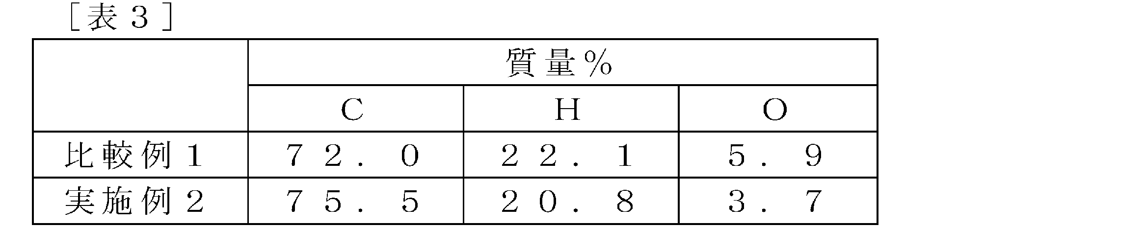
- the resist underlayer film formed by baking at 350 ° C. in a nitrogen atmosphere has an increased carbon concentration as compared with the resist underlayer film formed by baking at 240 ° C. in air. It can be seen that the oxygen concentration is decreasing.
Landscapes
- Chemical & Material Sciences (AREA)
- Organic Chemistry (AREA)
- Physics & Mathematics (AREA)
- General Physics & Mathematics (AREA)
- Engineering & Computer Science (AREA)
- Architecture (AREA)
- Structural Engineering (AREA)
- Spectroscopy & Molecular Physics (AREA)
- Wood Science & Technology (AREA)
- Materials Engineering (AREA)
- Life Sciences & Earth Sciences (AREA)
- Health & Medical Sciences (AREA)
- Chemical Kinetics & Catalysis (AREA)
- Medicinal Chemistry (AREA)
- Polymers & Plastics (AREA)
- Materials For Photolithography (AREA)
- Photosensitive Polymer And Photoresist Processing (AREA)
- Exposure Of Semiconductors, Excluding Electron Or Ion Beam Exposure (AREA)
- Exposure And Positioning Against Photoresist Photosensitive Materials (AREA)
- Organic Low-Molecular-Weight Compounds And Preparation Thereof (AREA)
Abstract
Description
フラーレン1分子に対して下記式(1):
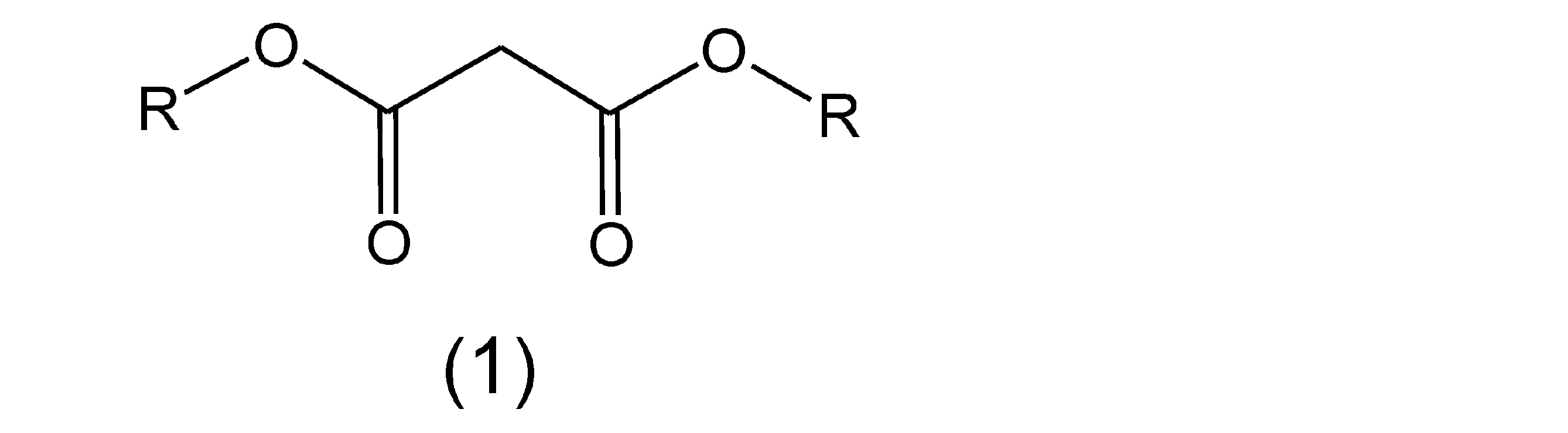
(式中、2つのRはそれぞれ独立に炭素原子数1乃至10のアルキル基を表す。)
で表されるマロン酸ジエステルが1乃至6分子付加したフラーレン誘導体、エポキシ基を少なくとも2つ有する化合物及び溶剤を含むレジスト下層膜形成組成物を基板上に塗布し、前記レジスト下層膜形成組成物が塗布された基板を、窒素、アルゴン又はそれらの混合物の雰囲気下で240℃以上の温度で少なくとも1回ベークする、レジスト下層膜の形成方法である。
前記レジスト下層膜上に中間層形成組成物を塗布し、ベークすることにより珪素含有中間層を形成する工程と、
前記珪素含有中間層上にレジスト膜を形成する工程と、
前記レジスト膜に対し少なくとも露光及び現像してレジストパターンを形成する工程と、
前記レジストパターンをマスクとして、フルオロカーボンを含むガスを用いて前記珪素含有中間層をドライエッチングする工程を有する、パターン形成方法である。
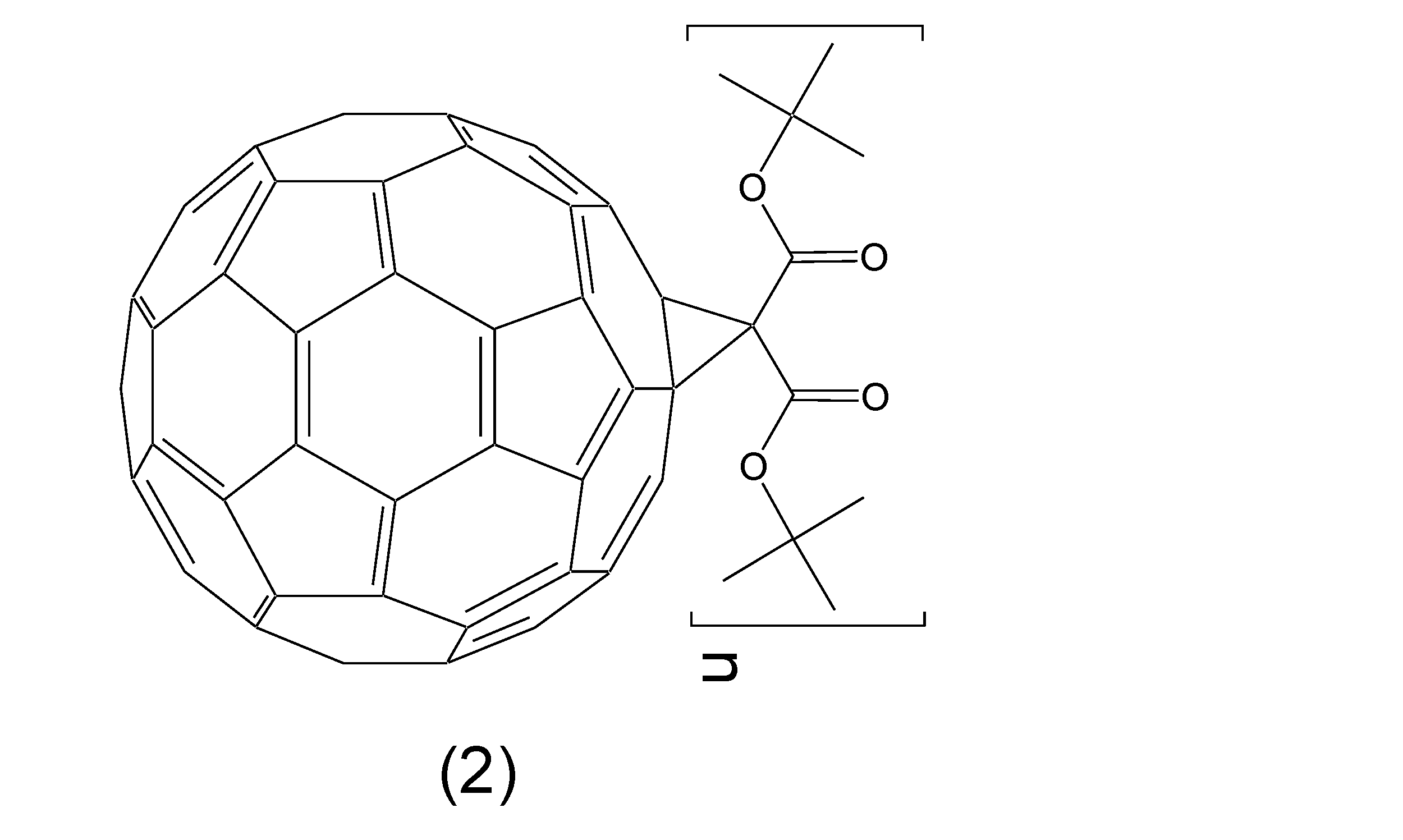
(式中、nは1乃至6の整数を表す。)
で表される化合物である。しかし、前記フラーレン誘導体は、この式(2)で表されるフラーレン誘導体に特定されるわけではない。
反応容器に窒素気流下マロン酸-ジ-tert-ブチル(Aldrich社製)9.80gを入れ、さらに1,2,4-トリメチルベンゼン150cm3とジアザビシクロ[5.4.0]-7-ウンデセン(1,8-diazabicyclo[5.4.0]undec-7-ene、東京化成工業株式会社製)6.50gを加えて撹拌しながら、温度を4℃に調整した。
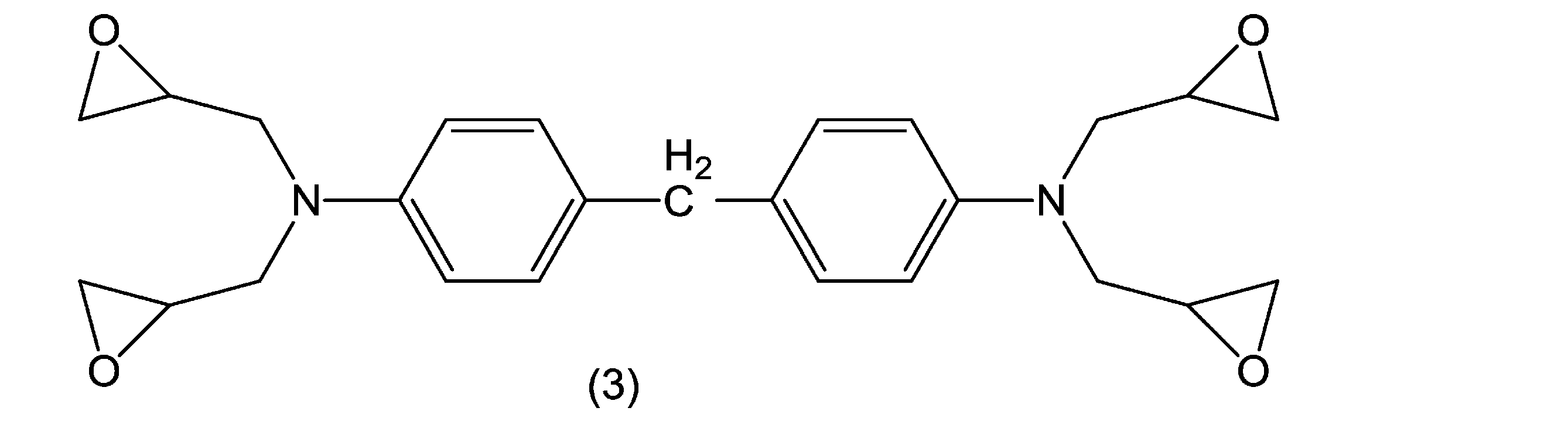
合成例1で得たフラーレン誘導体1.0gに、下記式(3)で表されるエポキシ化合物(新日化エポキシ製造株式会社製、商品名:YH434L)0.15g、界面活性剤としてメガファック〔登録商標〕R-40(DIC株式会社)0.001gを混合し、プロピレングリコールモノメチルエーテルアセテート7.0gに溶解させ溶液とした。その後、孔径0.10μmのポリエチレン製ミクロフィルターを用いてろ過し、更に、孔径0.05μmのポリエチレン製ミクロフィルターを用いてろ過して、レジスト下層膜形成組成物(溶液)を調製した。
クレゾールノボラック樹脂(市販品、重量平均分子量は4,000)1gに、プロピレングリコールモノメチルエーテル10.34g及びシクロヘキサノン2.59gを加えて溶解させ、多層膜によるリソグラフィープロセスに用いるレジスト下層膜形成組成物(溶液)を調製した。
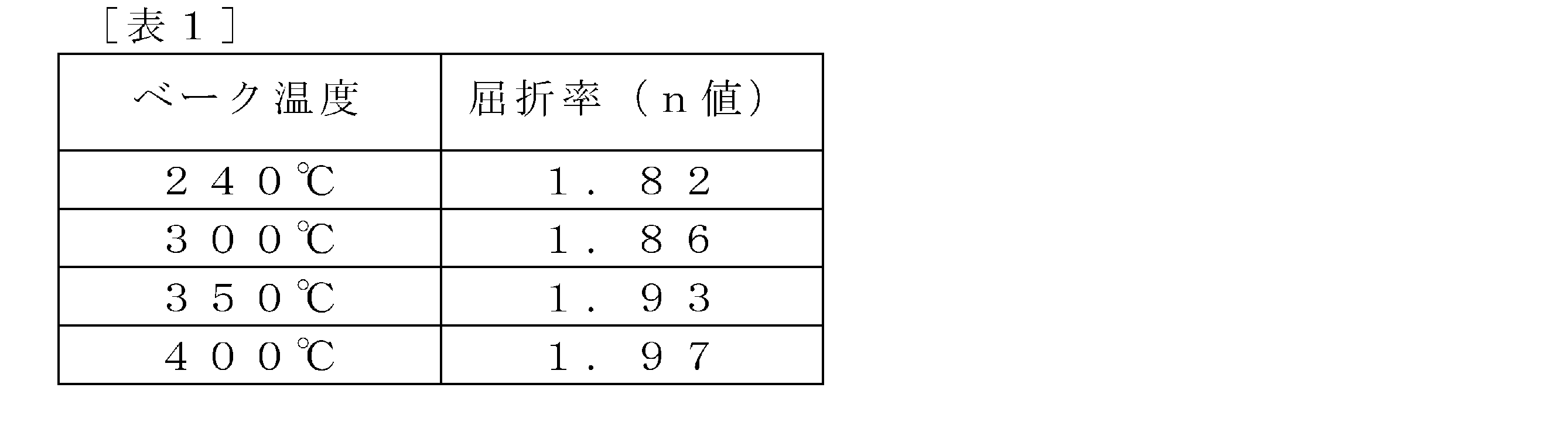
形成されたレジスト下層膜を、それぞれ分光エリプソメーター(J.A. Woollam社製、VUV-VASE VU-302)を用いて波長633nmでの屈折率(n値)を測定した。その結果を下記表1に示す。ベーク温度が高くなるほど、n値も高くなり、膜密度が向上することを示唆している。
ドライエッチング速度の測定には、下記のエッチング装置及びエッチングガスを用いた。
エッチング装置:RIE-10NR(サムコ株式会社製)
エッチングガス:CF4
実施例1、実施例2、比較例1及び比較例2のレジスト下層膜のドライエッチング速度を測定した。さらに、比較調製例1で得たレジスト下層膜形成組成物から形成されたレジスト下層膜のドライエッチング速度を測定し、後者のドライエッチング速度を1としたときの前者のドライエッチング速度を算出し、これをドライエッチング速度比と表した。その結果を下記表2に示す。

比較例1及び実施例2のレジスト下層膜について、元素分析を行った。元素分析結果は下記表3に示すとおりである。元素分析は、下記のラザフォード後方散乱分光(RBS)装置を用いて行った。
分析装置:高分解能RBS装置 HRBS500(株式会社神戸製鋼所製)
Claims (5)
- フラーレン1分子に対して下記式(1):

(式中、2つのRはそれぞれ独立に炭素原子数1乃至10のアルキル基を表す。)
で表されるマロン酸ジエステルが1乃至6分子付加したフラーレン誘導体、エポキシ基を少なくとも2つ有する化合物及び溶剤を含むレジスト下層膜形成組成物を基板上に塗布し、前記レジスト下層膜形成組成物が塗布された基板を、窒素、アルゴン又はそれらの混合物の雰囲気下で240℃以上の温度で少なくとも1回ベークする、レジスト下層膜の形成方法。 - 前記雰囲気下でのベーク温度は750℃以下である請求項1に記載のレジスト下層膜の形成方法。
- 前記雰囲気の酸素濃度は0.01ppm乃至100ppmである請求項1又は請求項2に記載のレジスト下層膜の形成方法。
- 前記レジスト下層膜形成組成物はさらに界面活性剤を含む請求項1乃至請求項3のいずれか一項に記載のレジスト下層膜の形成方法。
- 請求項1乃至請求項4のいずれか一項に記載の方法により形成されたレジスト下層膜上に中間層形成組成物を塗布し、ベークすることにより珪素含有中間層を形成する工程と、
前記珪素含有中間層上にレジスト膜を形成する工程と、
前記レジスト膜に対し少なくとも露光及び現像してレジストパターンを形成する工程と、
前記レジストパターンをマスクとして、フルオロカーボンを含むガスを用いて前記珪素含有中間層をドライエッチングする工程を有する、パターン形成方法。
Priority Applications (4)
| Application Number | Priority Date | Filing Date | Title |
|---|---|---|---|
| CN201680012680.6A CN107407883A (zh) | 2015-03-11 | 2016-02-05 | 抗蚀剂下层膜的形成方法 |
| KR1020177027786A KR102308765B1 (ko) | 2015-03-11 | 2016-02-05 | 레지스트 하층막의 형성방법 |
| US15/554,403 US10551737B2 (en) | 2015-03-11 | 2016-02-05 | Method for forming resist underlayer film |
| JP2017504921A JP6628052B2 (ja) | 2015-03-11 | 2016-02-05 | レジスト下層膜の形成方法 |
Applications Claiming Priority (2)
| Application Number | Priority Date | Filing Date | Title |
|---|---|---|---|
| JP2015-048760 | 2015-03-11 | ||
| JP2015048760 | 2015-03-11 |
Publications (1)
| Publication Number | Publication Date |
|---|---|
| WO2016143436A1 true WO2016143436A1 (ja) | 2016-09-15 |
Family
ID=56879349
Family Applications (1)
| Application Number | Title | Priority Date | Filing Date |
|---|---|---|---|
| PCT/JP2016/053534 Ceased WO2016143436A1 (ja) | 2015-03-11 | 2016-02-05 | レジスト下層膜の形成方法 |
Country Status (6)
| Country | Link |
|---|---|
| US (1) | US10551737B2 (ja) |
| JP (1) | JP6628052B2 (ja) |
| KR (1) | KR102308765B1 (ja) |
| CN (1) | CN107407883A (ja) |
| TW (1) | TWI689785B (ja) |
| WO (1) | WO2016143436A1 (ja) |
Cited By (2)
| Publication number | Priority date | Publication date | Assignee | Title |
|---|---|---|---|---|
| JP2017533464A (ja) * | 2014-10-08 | 2017-11-09 | アレックス フィリップ グラハム ロビンソンAlex Philip Graham ROBINSON | スピンオンハードマスク材料 |
| EP4239408A1 (en) | 2022-03-03 | 2023-09-06 | Shin-Etsu Chemical Co., Ltd. | Composition for forming organic film, patterning process, and compound |
Families Citing this family (3)
| Publication number | Priority date | Publication date | Assignee | Title |
|---|---|---|---|---|
| US11298249B2 (en) | 2018-06-07 | 2022-04-12 | Ossur Iceland Ehf | Prosthetic interface |
| CN109426100B (zh) * | 2018-10-29 | 2019-08-30 | 福建泓光半导体材料有限公司 | 一种耐刻蚀的光刻胶及其制备方法和应用以及光刻方法 |
| JP7390964B2 (ja) * | 2019-05-27 | 2023-12-04 | 信越化学工業株式会社 | 有機膜形成用材料、半導体装置製造用基板、及び有機膜の形成方法 |
Citations (9)
| Publication number | Priority date | Publication date | Assignee | Title |
|---|---|---|---|---|
| JP2000194128A (ja) * | 1998-12-28 | 2000-07-14 | Toshiba Corp | パタ―ントランスファ組成物及びパタ―ントランスファ方法 |
| WO2008062888A1 (en) * | 2006-11-20 | 2008-05-29 | Jsr Corporation | Composition for resist lower layer film formation and method for pattern formation |
| JP2008164806A (ja) * | 2006-12-27 | 2008-07-17 | Jsr Corp | レジスト下層膜形成用組成物及びパターン形成方法 |
| JP2009120538A (ja) * | 2007-11-15 | 2009-06-04 | Mitsubishi Chemicals Corp | フラーレン誘導体並びにその溶液及び膜 |
| JP2011150023A (ja) * | 2010-01-19 | 2011-08-04 | Shin-Etsu Chemical Co Ltd | レジスト下層膜形成用組成物、レジスト下層膜形成方法、及びパターン形成方法 |
| JP2011164201A (ja) * | 2010-02-05 | 2011-08-25 | Shin-Etsu Chemical Co Ltd | レジスト下層膜材料、レジスト下層膜形成方法、パターン形成方法、フラーレン誘導体 |
| WO2011108365A1 (ja) * | 2010-03-01 | 2011-09-09 | 日産化学工業株式会社 | フラーレン誘導体を含むレジスト下層膜形成組成物 |
| JP2012042895A (ja) * | 2010-08-23 | 2012-03-01 | Shin Etsu Chem Co Ltd | レジスト下層膜材料、レジスト下層膜形成方法、パターン形成方法、フラーレン誘導体 |
| WO2013117908A1 (en) * | 2012-02-10 | 2013-08-15 | The University Of Birmingham | Spin on hard-mask material |
Family Cites Families (6)
| Publication number | Priority date | Publication date | Assignee | Title |
|---|---|---|---|---|
| US5759666A (en) * | 1995-12-21 | 1998-06-02 | Minnesota Mining And Manufacturing Company | Carboxylic acid functional polyurethane polymers and blends thereof used in magnetic recording media |
| WO2005097883A2 (en) * | 2004-03-26 | 2005-10-20 | King Industries, Inc. | Method of producing a crosslinked coating in the manufacture of integrated circuits |
| US7745104B2 (en) * | 2006-08-10 | 2010-06-29 | Shin-Etsu Chemical Co., Ltd. | Bottom resist layer composition and patterning process using the same |
| US8361694B2 (en) * | 2007-04-06 | 2013-01-29 | Nissan Chemical Industries, Ltd. | Resist underlayer film forming composition |
| JP5077569B2 (ja) * | 2007-09-25 | 2012-11-21 | 信越化学工業株式会社 | パターン形成方法 |
| US20130194668A1 (en) * | 2012-01-30 | 2013-08-01 | Guardian Industries Corp. | Method of making coated article including anti-reflection coating with double coating layers including mesoporous materials, and products containing the same |
-
2016
- 2016-02-05 JP JP2017504921A patent/JP6628052B2/ja active Active
- 2016-02-05 KR KR1020177027786A patent/KR102308765B1/ko active Active
- 2016-02-05 US US15/554,403 patent/US10551737B2/en active Active
- 2016-02-05 CN CN201680012680.6A patent/CN107407883A/zh active Pending
- 2016-02-05 WO PCT/JP2016/053534 patent/WO2016143436A1/ja not_active Ceased
- 2016-02-18 TW TW105104770A patent/TWI689785B/zh active
Patent Citations (9)
| Publication number | Priority date | Publication date | Assignee | Title |
|---|---|---|---|---|
| JP2000194128A (ja) * | 1998-12-28 | 2000-07-14 | Toshiba Corp | パタ―ントランスファ組成物及びパタ―ントランスファ方法 |
| WO2008062888A1 (en) * | 2006-11-20 | 2008-05-29 | Jsr Corporation | Composition for resist lower layer film formation and method for pattern formation |
| JP2008164806A (ja) * | 2006-12-27 | 2008-07-17 | Jsr Corp | レジスト下層膜形成用組成物及びパターン形成方法 |
| JP2009120538A (ja) * | 2007-11-15 | 2009-06-04 | Mitsubishi Chemicals Corp | フラーレン誘導体並びにその溶液及び膜 |
| JP2011150023A (ja) * | 2010-01-19 | 2011-08-04 | Shin-Etsu Chemical Co Ltd | レジスト下層膜形成用組成物、レジスト下層膜形成方法、及びパターン形成方法 |
| JP2011164201A (ja) * | 2010-02-05 | 2011-08-25 | Shin-Etsu Chemical Co Ltd | レジスト下層膜材料、レジスト下層膜形成方法、パターン形成方法、フラーレン誘導体 |
| WO2011108365A1 (ja) * | 2010-03-01 | 2011-09-09 | 日産化学工業株式会社 | フラーレン誘導体を含むレジスト下層膜形成組成物 |
| JP2012042895A (ja) * | 2010-08-23 | 2012-03-01 | Shin Etsu Chem Co Ltd | レジスト下層膜材料、レジスト下層膜形成方法、パターン形成方法、フラーレン誘導体 |
| WO2013117908A1 (en) * | 2012-02-10 | 2013-08-15 | The University Of Birmingham | Spin on hard-mask material |
Cited By (3)
| Publication number | Priority date | Publication date | Assignee | Title |
|---|---|---|---|---|
| JP2017533464A (ja) * | 2014-10-08 | 2017-11-09 | アレックス フィリップ グラハム ロビンソンAlex Philip Graham ROBINSON | スピンオンハードマスク材料 |
| EP4239408A1 (en) | 2022-03-03 | 2023-09-06 | Shin-Etsu Chemical Co., Ltd. | Composition for forming organic film, patterning process, and compound |
| US12584023B2 (en) | 2022-03-03 | 2026-03-24 | Shin-Etsu Chemical Co., Ltd. | Composition for forming organic film, patterning process, and compound |
Also Published As
| Publication number | Publication date |
|---|---|
| US20180046078A1 (en) | 2018-02-15 |
| KR20170126967A (ko) | 2017-11-20 |
| TW201704881A (zh) | 2017-02-01 |
| JPWO2016143436A1 (ja) | 2017-12-21 |
| TWI689785B (zh) | 2020-04-01 |
| KR102308765B1 (ko) | 2021-10-05 |
| CN107407883A (zh) | 2017-11-28 |
| US10551737B2 (en) | 2020-02-04 |
| JP6628052B2 (ja) | 2020-01-08 |
Similar Documents
| Publication | Publication Date | Title |
|---|---|---|
| JP5757286B2 (ja) | フラーレン誘導体を含むレジスト下層膜形成組成物 | |
| KR101342024B1 (ko) | 나프탈렌 수지 유도체를 함유하는 리소그래피용 도포형 하층막 형성 조성물 | |
| JP6628052B2 (ja) | レジスト下層膜の形成方法 | |
| TWI865446B (zh) | 半導體基板用底漆及圖型形成方法 | |
| KR20140012111A (ko) | 레지스트 하층막 형성 조성물 및 이를 이용한 레지스트 패턴의 형성 방법 | |
| KR101684870B1 (ko) | 단분자층 또는 다분자층 형성용 조성물 | |
| KR102643360B1 (ko) | 레지스트 하층막 형성 조성물 | |
| KR102334790B1 (ko) | 나프톨아랄킬 수지를 포함하는 레지스트 하층막 형성 조성물 | |
| KR102324679B1 (ko) | 금속 산화물을 함유하는 재료, 이것의 제조 방법 및 이것의 사용 방법 | |
| TW202328817A (zh) | 光阻下層膜形成組成物 | |
| JP2017097240A (ja) | ケイ素含有膜形成用材料及びパターン形成方法 | |
| JP5835593B2 (ja) | シラン化合物及びそれを用いた単分子層又は多分子層形成用組成物 | |
| JP2022132962A (ja) | レジスト下層膜形成組成物 | |
| JP7301151B2 (ja) | 下層膜形成用組成物、レジストパターン形成方法、電子デバイスの製造方法 | |
| TWI850464B (zh) | 預濕液、抗蝕劑膜形成方法、圖案形成方法、套組 | |
| TW202602977A (zh) | 阻劑下層膜形成用組成物 | |
| JPWO2017154545A1 (ja) | レジストプロセス用膜形成材料、パターン形成方法及び重合体 | |
| TW202602963A (zh) | 阻劑下層膜形成用組成物 | |
| WO2024024490A1 (ja) | レジスト下層膜形成用組成物 |
Legal Events
| Date | Code | Title | Description |
|---|---|---|---|
| 121 | Ep: the epo has been informed by wipo that ep was designated in this application |
Ref document number: 16761408 Country of ref document: EP Kind code of ref document: A1 |
|
| ENP | Entry into the national phase |
Ref document number: 2017504921 Country of ref document: JP Kind code of ref document: A |
|
| WWE | Wipo information: entry into national phase |
Ref document number: 15554403 Country of ref document: US |
|
| NENP | Non-entry into the national phase |
Ref country code: DE |
|
| ENP | Entry into the national phase |
Ref document number: 20177027786 Country of ref document: KR Kind code of ref document: A |
|
| 122 | Ep: pct application non-entry in european phase |
Ref document number: 16761408 Country of ref document: EP Kind code of ref document: A1 |