WO2016143368A1 - リアクトル、接続部材、基板モジュール、および電気機器 - Google Patents
リアクトル、接続部材、基板モジュール、および電気機器 Download PDFInfo
- Publication number
- WO2016143368A1 WO2016143368A1 PCT/JP2016/050713 JP2016050713W WO2016143368A1 WO 2016143368 A1 WO2016143368 A1 WO 2016143368A1 JP 2016050713 W JP2016050713 W JP 2016050713W WO 2016143368 A1 WO2016143368 A1 WO 2016143368A1
- Authority
- WO
- WIPO (PCT)
- Prior art keywords
- substrate
- connection member
- electronic component
- connection
- spiral
- Prior art date
- Legal status (The legal status is an assumption and is not a legal conclusion. Google has not performed a legal analysis and makes no representation as to the accuracy of the status listed.)
- Ceased
Links
Images

Classifications
-
- H—ELECTRICITY
- H05—ELECTRIC TECHNIQUES NOT OTHERWISE PROVIDED FOR
- H05K—PRINTED CIRCUITS; CASINGS OR CONSTRUCTIONAL DETAILS OF ELECTRIC APPARATUS; MANUFACTURE OF ASSEMBLAGES OF ELECTRICAL COMPONENTS
- H05K1/00—Printed circuits
- H05K1/02—Details
- H05K1/0213—Electrical arrangements not otherwise provided for
- H05K1/0216—Reduction of cross-talk, noise or electromagnetic interference
- H05K1/023—Reduction of cross-talk, noise or electromagnetic interference using auxiliary mounted passive components or auxiliary substances
- H05K1/0233—Filters, inductors or a magnetic substance
-
- H—ELECTRICITY
- H01—ELECTRIC ELEMENTS
- H01F—MAGNETS; INDUCTANCES; TRANSFORMERS; SELECTION OF MATERIALS FOR THEIR MAGNETIC PROPERTIES
- H01F27/00—Details of transformers or inductances, in general
- H01F27/06—Mounting, supporting, or suspending transformers, reactors, or choke coils not being of the signal type
-
- H—ELECTRICITY
- H01—ELECTRIC ELEMENTS
- H01F—MAGNETS; INDUCTANCES; TRANSFORMERS; SELECTION OF MATERIALS FOR THEIR MAGNETIC PROPERTIES
- H01F27/00—Details of transformers or inductances, in general
- H01F27/08—Cooling; Ventilating
- H01F27/22—Cooling by heat conduction through solid or powdered fillings
-
- H—ELECTRICITY
- H01—ELECTRIC ELEMENTS
- H01F—MAGNETS; INDUCTANCES; TRANSFORMERS; SELECTION OF MATERIALS FOR THEIR MAGNETIC PROPERTIES
- H01F27/00—Details of transformers or inductances, in general
- H01F27/24—Magnetic cores
-
- H—ELECTRICITY
- H01—ELECTRIC ELEMENTS
- H01F—MAGNETS; INDUCTANCES; TRANSFORMERS; SELECTION OF MATERIALS FOR THEIR MAGNETIC PROPERTIES
- H01F27/00—Details of transformers or inductances, in general
- H01F27/28—Coils; Windings; Conductive connections
-
- H—ELECTRICITY
- H01—ELECTRIC ELEMENTS
- H01F—MAGNETS; INDUCTANCES; TRANSFORMERS; SELECTION OF MATERIALS FOR THEIR MAGNETIC PROPERTIES
- H01F27/00—Details of transformers or inductances, in general
- H01F27/28—Coils; Windings; Conductive connections
- H01F27/29—Terminals; Tapping arrangements for signal inductances
-
- H—ELECTRICITY
- H01—ELECTRIC ELEMENTS
- H01F—MAGNETS; INDUCTANCES; TRANSFORMERS; SELECTION OF MATERIALS FOR THEIR MAGNETIC PROPERTIES
- H01F27/00—Details of transformers or inductances, in general
- H01F27/40—Structural association with built-in electric component, e.g. fuse
-
- H—ELECTRICITY
- H01—ELECTRIC ELEMENTS
- H01F—MAGNETS; INDUCTANCES; TRANSFORMERS; SELECTION OF MATERIALS FOR THEIR MAGNETIC PROPERTIES
- H01F37/00—Fixed inductances not covered by group H01F17/00
-
- H—ELECTRICITY
- H05—ELECTRIC TECHNIQUES NOT OTHERWISE PROVIDED FOR
- H05K—PRINTED CIRCUITS; CASINGS OR CONSTRUCTIONAL DETAILS OF ELECTRIC APPARATUS; MANUFACTURE OF ASSEMBLAGES OF ELECTRICAL COMPONENTS
- H05K1/00—Printed circuits
- H05K1/02—Details
- H05K1/0213—Electrical arrangements not otherwise provided for
- H05K1/0263—High current adaptations, e.g. printed high current conductors or using auxiliary non-printed means; Fine and coarse circuit patterns on one circuit board
-
- H—ELECTRICITY
- H05—ELECTRIC TECHNIQUES NOT OTHERWISE PROVIDED FOR
- H05K—PRINTED CIRCUITS; CASINGS OR CONSTRUCTIONAL DETAILS OF ELECTRIC APPARATUS; MANUFACTURE OF ASSEMBLAGES OF ELECTRICAL COMPONENTS
- H05K3/00—Apparatus or processes for manufacturing printed circuits
- H05K3/36—Assembling printed circuits with other printed circuits
- H05K3/368—Assembling printed circuits with other printed circuits parallel to each other
-
- H—ELECTRICITY
- H05—ELECTRIC TECHNIQUES NOT OTHERWISE PROVIDED FOR
- H05K—PRINTED CIRCUITS; CASINGS OR CONSTRUCTIONAL DETAILS OF ELECTRIC APPARATUS; MANUFACTURE OF ASSEMBLAGES OF ELECTRICAL COMPONENTS
- H05K3/00—Apparatus or processes for manufacturing printed circuits
- H05K3/40—Forming printed elements for providing electric connections to or between printed circuits
-
- H—ELECTRICITY
- H01—ELECTRIC ELEMENTS
- H01F—MAGNETS; INDUCTANCES; TRANSFORMERS; SELECTION OF MATERIALS FOR THEIR MAGNETIC PROPERTIES
- H01F27/00—Details of transformers or inductances, in general
- H01F27/06—Mounting, supporting, or suspending transformers, reactors, or choke coils not being of the signal type
- H01F27/065—Mounting on printed circuit boards
-
- H—ELECTRICITY
- H01—ELECTRIC ELEMENTS
- H01F—MAGNETS; INDUCTANCES; TRANSFORMERS; SELECTION OF MATERIALS FOR THEIR MAGNETIC PROPERTIES
- H01F27/00—Details of transformers or inductances, in general
- H01F27/28—Coils; Windings; Conductive connections
- H01F27/2876—Cooling
-
- H—ELECTRICITY
- H05—ELECTRIC TECHNIQUES NOT OTHERWISE PROVIDED FOR
- H05K—PRINTED CIRCUITS; CASINGS OR CONSTRUCTIONAL DETAILS OF ELECTRIC APPARATUS; MANUFACTURE OF ASSEMBLAGES OF ELECTRICAL COMPONENTS
- H05K1/00—Printed circuits
- H05K1/02—Details
- H05K1/0201—Thermal arrangements, e.g. for cooling, heating or preventing overheating
- H05K1/0203—Cooling of mounted components
-
- H—ELECTRICITY
- H05—ELECTRIC TECHNIQUES NOT OTHERWISE PROVIDED FOR
- H05K—PRINTED CIRCUITS; CASINGS OR CONSTRUCTIONAL DETAILS OF ELECTRIC APPARATUS; MANUFACTURE OF ASSEMBLAGES OF ELECTRICAL COMPONENTS
- H05K1/00—Printed circuits
- H05K1/02—Details
- H05K1/14—Structural association of two or more printed circuits
- H05K1/142—Arrangements of planar printed circuit boards in the same plane, e.g. auxiliary printed circuit insert mounted in a main printed circuit
-
- H—ELECTRICITY
- H05—ELECTRIC TECHNIQUES NOT OTHERWISE PROVIDED FOR
- H05K—PRINTED CIRCUITS; CASINGS OR CONSTRUCTIONAL DETAILS OF ELECTRIC APPARATUS; MANUFACTURE OF ASSEMBLAGES OF ELECTRICAL COMPONENTS
- H05K2201/00—Indexing scheme relating to printed circuits covered by H05K1/00
- H05K2201/06—Thermal details
- H05K2201/066—Heatsink mounted on the surface of the printed circuit board [PCB]
-
- H—ELECTRICITY
- H05—ELECTRIC TECHNIQUES NOT OTHERWISE PROVIDED FOR
- H05K—PRINTED CIRCUITS; CASINGS OR CONSTRUCTIONAL DETAILS OF ELECTRIC APPARATUS; MANUFACTURE OF ASSEMBLAGES OF ELECTRICAL COMPONENTS
- H05K2201/00—Indexing scheme relating to printed circuits covered by H05K1/00
- H05K2201/10—Details of components or other objects attached to or integrated in a printed circuit board
- H05K2201/10007—Types of components
- H05K2201/1003—Non-printed inductor
-
- H—ELECTRICITY
- H05—ELECTRIC TECHNIQUES NOT OTHERWISE PROVIDED FOR
- H05K—PRINTED CIRCUITS; CASINGS OR CONSTRUCTIONAL DETAILS OF ELECTRIC APPARATUS; MANUFACTURE OF ASSEMBLAGES OF ELECTRICAL COMPONENTS
- H05K2201/00—Indexing scheme relating to printed circuits covered by H05K1/00
- H05K2201/10—Details of components or other objects attached to or integrated in a printed circuit board
- H05K2201/10007—Types of components
- H05K2201/10053—Switch
-
- H—ELECTRICITY
- H05—ELECTRIC TECHNIQUES NOT OTHERWISE PROVIDED FOR
- H05K—PRINTED CIRCUITS; CASINGS OR CONSTRUCTIONAL DETAILS OF ELECTRIC APPARATUS; MANUFACTURE OF ASSEMBLAGES OF ELECTRICAL COMPONENTS
- H05K2201/00—Indexing scheme relating to printed circuits covered by H05K1/00
- H05K2201/10—Details of components or other objects attached to or integrated in a printed circuit board
- H05K2201/10007—Types of components
- H05K2201/1006—Non-printed filter
-
- H—ELECTRICITY
- H05—ELECTRIC TECHNIQUES NOT OTHERWISE PROVIDED FOR
- H05K—PRINTED CIRCUITS; CASINGS OR CONSTRUCTIONAL DETAILS OF ELECTRIC APPARATUS; MANUFACTURE OF ASSEMBLAGES OF ELECTRICAL COMPONENTS
- H05K2201/00—Indexing scheme relating to printed circuits covered by H05K1/00
- H05K2201/10—Details of components or other objects attached to or integrated in a printed circuit board
- H05K2201/10227—Other objects, e.g. metallic pieces
- H05K2201/10265—Metallic coils or springs, e.g. as part of a connection element
-
- H—ELECTRICITY
- H05—ELECTRIC TECHNIQUES NOT OTHERWISE PROVIDED FOR
- H05K—PRINTED CIRCUITS; CASINGS OR CONSTRUCTIONAL DETAILS OF ELECTRIC APPARATUS; MANUFACTURE OF ASSEMBLAGES OF ELECTRICAL COMPONENTS
- H05K2201/00—Indexing scheme relating to printed circuits covered by H05K1/00
- H05K2201/10—Details of components or other objects attached to or integrated in a printed circuit board
- H05K2201/10227—Other objects, e.g. metallic pieces
- H05K2201/10272—Busbars, i.e. thick metal bars mounted on the printed circuit board [PCB] as high-current conductors
Definitions
- the present invention relates to a connection member, a reactor, a board module, and an electric device.
- Patent Literature 1 Japanese Patent Application Laid-Open No. 2012-164878
- connection points such as connection points between terminals and wiring.
- connection points When a relatively large pulse current flows through the lead wire, radiation noise is generated at the connection points, so it is preferable that the number of connection points is small.
- a reactor according to one embodiment of the present invention includes a winding, a magnetic core of the winding, and an electrical connection that extends from the winding, and at least a portion between the winding and the electronic component is spiral.
- the winding member and the connection member are formed of one conductive member.
- one conductive member may be a single bar member or a single plate member.
- the electronic component may be a substrate, and the end of the connection member may be directly fixed to the substrate.
- the electronic component may be a board, and the end of the connection member may be directly fixed to a terminal block on the board.
- connection member extends from one end of the winding and has at least a portion formed in a spiral shape, and the connection member extends from the other end of the winding and at least a portion formed in a spiral shape.
- the spiral portion of the first spiral portion and the spiral portion of the second spiral portion may be arranged to face each other.
- the spiral part of the first spiral part and the spiral part of the second spiral part may have the same shape.
- a substrate module includes the reactor and a substrate that is an electronic component electrically connected to the reactor.
- the substrate may include a switch circuit, and the switch circuit may input a pulse current to the reactor.
- An electric apparatus includes a housing having the substrate module, a first fixing member to which the reactor is fixed, and a second fixing member to which the substrate is fixed.
- a connection member is a connection member that electrically connects a first electronic component and a second electronic component, and is formed of one conductive member, and one end is electrically connected to the first electronic component. , The other end is electrically connected to the second electronic component, and at least a part between the one end and the other end is formed in a spiral shape.
- one conductive member may be a single bar member or a single plate member.
- the first electronic component may be a first substrate, and one end may be directly fixed to the first substrate.
- the first electronic component may be a first substrate, and one end may be directly fixed to a terminal block on the first substrate.
- the second electronic component may be a second substrate, and the other end may be directly fixed to the second substrate.
- the second electronic component may be a second substrate, and the other end may be directly fixed to a terminal block on the second substrate.
- a substrate module is the above-described connection member, a first electronic component, a first substrate having a first electric circuit, and a second electronic component, with the first electric circuit and the connection member interposed therebetween. And a second substrate having a second electric circuit electrically connected thereto.
- At least one of the first electric circuit and the second electric circuit includes a switch circuit, and the connection member transmits a pulse current output from the switch circuit between the first board and the second board. You can do it.
- At least one of the first electric circuit and the second electric circuit may include a noise filter circuit.
- An electrical apparatus includes a substrate module, a housing having a first fixing member to which the first substrate is fixed, and a second fixing member to which the second substrate is fixed.
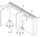
- FIG. 1 is an external perspective view showing an example of a board module 1000 according to the present embodiment.
- the board module 1000 includes a board 10, a board 20, a board 30, a connection member 100, and a connection member 200.
- the substrate 10, the substrate 20, and the substrate 30 each have an electric circuit.
- the electric circuit includes a switch circuit, a reactor, a noise filter circuit, and the like.
- the switch circuit may be a power module such as an IGBT module or a power MOSFET module.
- substrate 20 may be fixed to the heat sink 50 which is an example of a fixing member.
- substrate 30 may be fixed to the inner wall of the housing
- the inner wall of the housing is an example of a fixing member.
- the board module 1000 may be mounted on an electric device through which a relatively large current (for example, 1 A or more) flows.
- the substrate module 1000 may be mounted on an electrical device in which a pulse current flows by being switched by a switch circuit.
- the electric device may be, for example, a power conversion device such as a power conditioner, a motor drive device, a power supply device, or the like.
- the lead member is often used as the connection member for electrically connecting the substrates.
- Lead wires are manufactured by caulking terminal portions such as round terminals or Y terminals at both ends of an electric wire. When a relatively large pulse current flows through such a lead wire, radiation noise is generated at the connection point between the electric wire and the terminal portion. Radiated noise may adversely affect electronic circuits mounted on the board module 1000 or other external devices.
- the generation of radiation noise is suppressed by reducing the number of connection parts of connection members that electrically connect electronic components such as substrates.
- the connecting member 100 electrically and mechanically connects the substrate 10 and the substrate 20, and transmits current between the substrate 10 and the substrate 20.
- the substrate 10 is an example of a first electronic component and a first substrate
- the substrate 20 is an example of a second electronic component and a second substrate.
- the resistance value of the connecting member 100 is preferably low, for example, in order to efficiently transmit current while suppressing energy loss.
- the resistance value per unit length of the connecting member 100 is selected from the viewpoint of loss and heat generation depending on the amount of current to flow, but is preferably a low value.
- the connection member 100 is formed of one conductive member made of metal such as copper, copper alloy, or aluminum.
- One conductive member is preferably a material that does not apply a force and does not deform in shape.
- One conductive member may be a single bar member or a single plate member.
- connection member 100 is electrically connected to the substrate 10, and the other end of the connection member 100 is electrically connected to the substrate 20.
- One end of the connection member 100 may be mechanically directly connected to the substrate 10 by soldering or the like.
- One end of the connection member 100 may be mechanically directly connected to a terminal block on the substrate 10.
- one end of the connection member 100 may be indirectly and mechanically connected to the substrate 10 via a terminal such as a round terminal or a Y terminal separate from the connection member 100.
- the other end of the connection member 100 may be mechanically directly connected to the substrate 20 by soldering or the like.
- the other end of the connection member 100 may be mechanically directly connected to a terminal block on the substrate 20.
- the other end of the connection member 100 may be indirectly and mechanically connected to the substrate 20 via a terminal such as a round terminal or a Y terminal that is separate from the connection member 100.
- the connecting member 100 is formed in a spiral shape at least partly between one end and the other end.
- the connecting member 100 may be integrally formed by deforming one bar member or one plate member.
- connection member 200 electrically and mechanically connects the substrate 10 and the substrate 30 and transmits a current between the substrate 10 and the substrate 30.
- the connecting member 100 may transmit a pulse current between the substrate 10 and the substrate 20.
- the connection member 200 is formed of one conductive member such as a metal such as copper or a copper alloy.
- the connection member 100 includes a first connection part 104, a spiral part 102, and a second connection part 106.
- the first connection portion 104, the spiral portion 102, and the second connection portion 106 are integrally formed of one conductive member.
- the connecting member 100 may be formed by deforming a metal plate such as a single copper plate or a metal bar such as a single copper rod.
- the first connection portion 104 includes one end of the connection member 100 and is electrically and mechanically connected to the substrate 10.
- the first connection portion 104 may be directly fixed to the substrate 10 with solder.
- the first connection portion 104 has a terminal such as a round terminal or a Y terminal at an end portion, and is directly fixed to a terminal block provided on the substrate 10 using a screw or the like. May be connected.
- the spiral portion 102 extends from the first connection portion 104 and is formed integrally with the first connection portion 104, and at least a part thereof is spiral.
- the spiral portion 102 is formed by bending a plate-like or rod-like member into a winding shape at least half a turn or more than one turn.
- the spiral portion 102 may function as an air-core coil.
- the second connection portion 106 includes the other end of the connection member 100, extends from the side opposite to the first connection portion 104 of the spiral portion 102, is integrally formed with the spiral portion 102, and is electrically and mechanically connected to the substrate 20. Connected to.
- the second connection portion 106 may be directly fixed to the substrate 20 with solder.
- the second connection portion 106 has a terminal such as a round terminal or a Y terminal at the end, and is directly fixed to a terminal block provided on the substrate 20 using a screw or the like. May be connected.
- the 1st connection part 104, the spiral part 102, and the 2nd connection part 106 are integrally formed by deform
- the first connection portion 104, the spiral portion 102, and the second connection portion 106 may be integrally formed by deforming one metal plate or one metal rod. Therefore, radiation noise does not occur at the connection point between the terminal and the electric wire unlike the conventional lead wire.
- the conductive member is preferably a metal such as copper.
- the connection member 100 is formed of such a metal plate or metal rod, a certain degree of thickness or thickness is required in order to suppress the resistance to some extent. Therefore, the rigidity of the connecting member 100 is relatively high.
- the connecting member 100 is more rigid than the lead wire.
- the connecting member 100 has higher rigidity than a lead wire that is bundled with a plurality of electric wires such as thin copper wires and mechanically and electrically connected to the end portion by caulking a connection terminal.
- the rigidity of the connecting member 100 is ten times higher than the rigidity of such a lead wire.
- the connecting member 100 is more rigid than a lead wire having a rated voltage of 300 V or more and a maximum conductor resistance of 22.6 ⁇ / km or less, which is used when a relatively large current, for example, a pulse current of 10 A or more is passed. high.
- connecting member 100 in order to flow the above pulse current 30A, first connecting portion 104, spiral portion 102, the sectional area of the second connecting portion 106 is 8 mm 2 or more, more preferably 16 mm 2 More preferably, it is 30 mm 2 or more.
- the connection member 100 is preferably formed of a low-resistance conductive member in order to suppress heat generation due to current flow and suppress energy loss.
- a conductive member is preferably, for example, a metal such as copper, but such a metal has a Brinell hardness of HBW 80 to 150 in brass.
- the connection member 100 needs a certain length in order to connect the substrates. Thus, a structure having a large cross-sectional area, a high Young's modulus, and a certain length has high rigidity.
- the substrate module 1000 may be mounted in a housing.
- the substrate 10, the substrate 20, and the substrate 30 included in the substrate module 1000 may be fixed to separate fixing members in the housing.
- the substrate 10 and the substrate 20 may be fixed to the heat sink 50 incorporated in the housing, and the substrate 30 may be fixed to the inner wall of the housing via a column or the like.
- each of the plurality of fixing members may vibrate independently. If the rigidity of the connection member that mechanically connects between the boards is large, a large force is applied to the connection part between the board and the connection member, and there is a possibility of adverse effects such as poor connection or cracks at the connection part between the board and the connection member. There is.
- the connection member 100 according to the present embodiment such vibration can be absorbed in the spiral portion 102. Therefore, even when the substrate 10 and the substrate 20 mechanically connected by the highly rigid connection member 100 vibrate independently from each other, there is an adverse effect such as a crack in the connection portion between the substrate 10 and the substrate 20 and the connection member 100. Occurrence can be suppressed.
- the connection member 200 includes a first connection portion 204, a spiral portion 202, and a second connection portion 206. Similar to the connection member 100, the first connection portion 204, the spiral portion 202, and the second connection portion 206 are integrally formed by deforming one conductive member. Similarly to the connection member 100, the connection member 200 may be formed by deforming, for example, a metal plate such as a single copper plate or a metal bar such as a single copper rod.
- connection member 200 even when the substrate 10 and the substrate 30 are arranged vertically, the number of turns of the spiral portion 202 is adjusted to adjust the shape of the spiral portion 202.
- the substrate 10 and the substrate 30 can be electrically and mechanically connected by the connecting member 200.
- the connection member 100 and the connection member 200 may be covered with a resin or the like.
- connection member 100 and the connection member 200 that electrically and mechanically connect electronic components such as a substrate are formed by deforming one bar-like or plate-like conductive member. Yes. Therefore, since the connection location between components can be reduced, radiation noise generated at the connection location can be reduced. Further, the connection member 100 and the connection member 200 are at least partially formed in a spiral shape. Thus, even when an electronic component such as a substrate mechanically connected to the connection member 100 or the connection member 200 vibrates, the vibration can be absorbed by the spiral portion of the connection member 100 or the connection member 200. Therefore, it is possible to reduce adverse effects such as a connection failure or a crack at a connection portion between the connection member 100 or the connection member 200 and the electronic component.
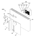
- FIG. 2 is an exploded perspective view showing an example of a substrate module 2000 according to another embodiment.
- the substrate module 2000 may be mounted on an electric device through which a relatively large current (for example, 10 A or more) flows.
- the substrate module 2000 may be mounted on an electric device in which a pulse current flows by being switched by a switch circuit.
- the electric device may be, for example, a power conversion device such as a power conditioner, a motor drive device, a power supply device, or the like.
- the substrate module 2000 includes a substrate 10, a substrate 20, and a reactor 300.
- Reactor 300 is electrically and mechanically connected to substrate 10 via heat sink 50.
- the substrate 10 is electrically connected to the substrate 20 through the connection member 100 described above.
- a reactor through which a relatively large current flows has a winding coil electrically connected to a substrate via a lead wire.
- the lead wire and the coil are caulked and fixed. Therefore, similarly to the connection between the substrates, in such a reactor, there is a high possibility that radiation noise is generated at the connection point between the coil and the lead wire. Therefore, in another embodiment, radiation noise generated in a reactor connected to an electronic component such as a substrate is reduced.
- the reactor 300 includes a winding 310, a magnetic core of the winding 310, and a connection member 320.
- the connection member 320 extends from the winding 310 and is electrically connected to the substrate 10, and at least a part between the winding 310 and the substrate 10 is formed in a spiral shape.
- the resistance values of the winding 310 and the connection member 320 are preferably low, for example, in order to efficiently transmit current while suppressing energy loss.
- the resistance values of the winding 310 and the connection member 320 are preferably 20 m ⁇ or less, more preferably 10 m ⁇ or less, and even more preferably 1 m ⁇ or less.
- the winding 310 and the connecting member 320 are formed of one conductive member such as a metal such as copper, copper alloy, gold, silver, or aluminum.
- One conductive member is preferably a material that does not easily deform.
- One conductive member may be a single bar member or a single plate member.
- the winding 310 and the connection member 320 may be integrally formed by deforming one bar member or one plate member. By forming the winding 310 and the connection member 320 in this way, the connection location between the winding 310 and the connection member 320 and the connection location of the connection member 320 can be reduced, thus reducing radiation noise generated at each connection location. it can.
- One end and the other end of the connection member 320 may be mechanically directly connected to the substrate 10 by soldering or the like.
- one end and the other end of the connection member 320 may be mechanically directly connected to the terminal block on the substrate 10.
- one end and the other end of the connection member 320 may be indirectly and mechanically connected to the substrate 10 via a terminal such as a round terminal or a Y terminal separate from the connection member 320.
- the connection member 320 includes a first connection part 322, a first spiral part 324, a second connection part 326, and a second spiral part 328.
- the first connection part 322 and the second connection part 326 may have terminals such as a round terminal and a Y terminal for connection to an electronic component such as the substrate 10.
- the first spiral portion 324 extends from one end of the winding 310 and is at least partially formed in a spiral shape.
- the second spiral portion 328 extends from the other end of the winding 310 and is at least partially formed in a spiral shape.
- the spiral portion of the first spiral portion 324 and the spiral portion of the second spiral portion 328 may have the same shape, and the first spiral portion 324 and the second spiral portion 328 may be disposed to face each other. .
- the direction of the current flowing through the first spiral portion 324 and the direction of the current flowing through the second spiral portion 328 are opposite to each other, so that the first spiral portion 324 and the second spiral portion 328 Even if radiation noise is generated, the radiation noise generated from each cancels out, so that the radiation noise can be further reduced. Therefore, by arranging the first spiral portion 324 and the second spiral portion 328 to face each other, the first spiral portion 324 and the second spiral portion 328 each function as an air-core coil and virtually function as a filter. be able to. Further, by arranging a magnetic core (core) inside each of the first spiral portion 324 and the second spiral portion 328, it can function as an AC filter or a DC filter.
- core magnetic core
- the heat sink 50 has a through hole 52 at a position facing the connection member 320 of the reactor 300.
- the substrate 10 has the through hole 16 at a position facing the connection member 320 of the reactor 300.
- the heat sink 50 is disposed between the reactor 300 and the substrate 10.
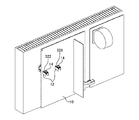
- the connection member 320 is connected to the substrate 10 through the through hole 52 and the through hole 16.
- the substrate 10 has a terminal block 12 disposed at a position facing the connection member 320. As shown in FIGS. 3 and 4, the first connection portion 322 and the second connection portion 326 are directly fixed to the terminal block 12 via the screws 14.
- connection member 320 is electrically and mechanically connected to the substrate 10 via the terminal block 12
- the reactor 300 may be electrically connected to the substrate 10 by directly fixing the first connection portion 322 and the second connection portion 326 to the substrate 10 with solder.
- the winding 310 and the connection member 320 are formed by one conductive member, a lead wire or the like is used for connection between the reactor 300 and the electronic component such as the substrate 10. Other members are unnecessary. Therefore, radiation noise generated at a connection location between components constituting other members such as a lead wire can be reduced.
- the connection member 320 is formed in a spiral shape, even if the substrate 10 or the reactor 300 vibrates, the vibration can be absorbed by the spiral portion of the connection member 320. Therefore, when the board
- Terminal block 14 Screw 50 Heat sink 100, 200 Connection member 102, 202 Spiral portion 104, 204 First connection portion 106, 206 Second connection portion 200 Connection member 300 Reactor 310 Winding 320 Connection member 322 First 1 connection part 324 1st spiral part 326 2nd connection part 328 2nd spiral part 1000 board module 2000 board module
Landscapes
- Engineering & Computer Science (AREA)
- Power Engineering (AREA)
- Microelectronics & Electronic Packaging (AREA)
- Manufacturing & Machinery (AREA)
- Physics & Mathematics (AREA)
- Electromagnetism (AREA)
- Dc-Dc Converters (AREA)
- Coils Of Transformers For General Uses (AREA)
- Power Conversion In General (AREA)
Abstract
電子部品間の接続部分での放射ノイズを低減する。リアクトルは、巻線と、巻線の磁心と、巻線から延伸して電子部品と電気的に接続し、巻線と電子部品との間の少なくとも一部が螺旋状に形成された接続部材とを備え、巻線および接続部材は、1つの導電部材で形成される。接続部材は、巻線の一端から延伸し、少なくとも一部が螺旋状に形成された第1螺旋部と、巻線の他端から延伸し、少なくとも一部が螺旋状に形成された第2螺旋部とを有し、第1螺旋部の螺旋状の部分と、第2螺旋部の螺旋状の部分とは、対向して配置されてよい。
Description
本発明は、接続部材、リアクトル、基板モジュール、および電気機器に関する。
特許文献1に示されているように、基板間または基板と電気回路との間は、例えば、リード線を介して接続されている。
特許文献1 特開2012-164878号公報
特許文献1 特開2012-164878号公報
上記のようなリード線は、端子と配線との接続点など複数の接続点がある。リード線に比較的大きなパルス電流などが流れる場合、接続点で放射ノイズが発生するので、接続点は少ないほうが好ましい。
本発明の一態様に係るリアクトルは、巻線と、巻線の磁心と、巻線から延伸して電子部品と電気的に接続し、巻線と電子部品との間の少なくとも一部が螺旋状に形成された接続部材とを備え、巻線及び接続部材は、1つの導電部材で形成される。
上記リアクトルにおいて、1つの導電部材は、一本の棒部材又は一枚の板部材でよい。
上記リアクトルにおいて、電子部品は、基板であり、接続部材の端部は、基板に直接固定されてよい。
上記リアクトルにおいて、電子部品は、基板であり、接続部材の端部は、基板上の端子台に直接固定されてよい。
上記リアクトルにおいて、接続部材は、巻線の一端から延伸し、少なくとも一部が螺旋状に形成された第1螺旋部と、巻線の他端から延伸し、少なくとも一部が螺旋状に形成された第2螺旋部とを有し、第1螺旋部の螺旋状の部分と、第2螺旋部の螺旋状の部分とは、対向して配置されていてよい。
上記リアクトルにおいて、第1螺旋部の螺旋状の部分と、第2螺旋部の螺旋状の部分とは、同一形状でよい。
本発明の一態様に係る基板モジュールは、上記リアクトルと、上記リアクトルと電気的に接続される電子部品である基板とを備える。
本発明の一態様に係る基板モジュールにおいて、基板は、スイッチ回路を含み、スイッチ回路は、パルス電流をリアクトルに入力してよい。
本発明の一態様に係る電気機器は、上記基板モジュールと、上記リアクトルが固定される第1固定部材と、上記基板が固定される第2固定部材と、を有する筐体を備える。
本発明の一態様に係る接続部材は、第1電子部品と第2電子部品とを電気的に接続する接続部材であって、1つの導電部材により形成され、一端が第1電子部品に電気的に接続され、他端が第2電子部品に電気的に接続され、一端と他端との間の少なくとも一部が螺旋状に形成されている。
上記接続部材において、1つの導電部材は、一本の棒部材又は一枚の板部材でよい。
上記接続部材において、第1電子部品は、第1基板であり、一端は、第1基板に直接固定されていてよい。
上記接続部品において、第1電子部品は、第1基板であり、一端は、第1基板上の端子台に直接固定されてよい。
上記接続部品において、第2電子部品は、第2基板であり、他端は、第2基板に直接固定されてよい。
上記接続部品は、第2電子部品は、第2基板であり、他端は、第2基板上の端子台に直接固定されてよい。
本発明の一態様に係る基板モジュールは、上記接続部材と、第1電子部品であり、第1電気回路を有する第1基板と、第2電子部品であり、第1電気回路と接続部材を介して電気的に接続される第2電気回路を有する第2基板とを備える。
上記基板モジュールにおいて、第1電気回路および第2電気回路の少なくとも一方は、スイッチ回路を含み、接続部材は、第1基板と第2基板との間で、スイッチ回路から出力されるパルス電流を伝達してよい。
上記基板モジュールにおいて、第1電気回路および第2電気回路の少なくとも一方は、ノイズフィルタ回路を含んでよい。
本発明の一態様に係る電気機器は、基板モジュールと、第1基板が固定される第1固定部材と、第2基板が固定される第2固定部材とを有する筐体とを備える。
なお、上記の発明の概要は、本発明の特徴の全てを列挙したものではない。また、これらの特徴群のサブコンビネーションもまた、発明となりうる。
以下、発明の実施の形態を通じて本発明を説明するが、以下の実施形態は請求の範囲にかかる発明を限定するものではない。また、実施形態の中で説明されている特徴の組み合わせの全てが発明の解決手段に必須であるとは限らない。
図1は、本実施形態に係る基板モジュール1000の一例を示す外観斜視図である。基板モジュール1000は、基板10、基板20、基板30、接続部材100、および接続部材200を備える。基板10、基板20、および基板30は、それぞれ電気回路を有する。電気回路は、スイッチ回路、リアクトル、ノイズフィルタ回路などを含む。スイッチ回路は、IGBTモジュール、パワーMOSFETモジュールなどのパワーモジュールでよい。基板10および基板20は、固定部材の一例であるヒートシンク50に固定されてよい。基板30は、ヒートシンク50とともに基板モジュールを内蔵する筐体の内壁に支柱などを介して固定されてよい。なお、筐体の内壁も固定部材の一例である。
基板モジュール1000は、比較的大きな電流(例えば、1A以上)が流れる電気機器に搭載されてよい。基板モジュール1000は、スイッチ回路によりスイッチングされることでパルス電流が流れる電気機器に搭載されてよい。電気機器は、例えば、パワーコンディショナなどの電力変換装置、モータ駆動機器、電源機器などでよい。
基板間を電気的に接続する接続部材は、リード線が用いられることが多い。リード線は、電線の両端に丸端子またはY端子などの端子部をかしめることで製造されている。このようなリード線に、比較的大きなパルス電流が流れる場合、電線と端子部との接続箇所で放射ノイズが発生する。放射ノイズは、基板モジュール1000に搭載される電子回路または外部の他の機器などに悪影響を与える可能性がある。
そこで、本実施形態では、基板などの電子部品間を電気的に接続する接続部材の接続箇所を削減することで、放射ノイズの発生を抑制する。
接続部材100は、基板10と基板20とを電気的かつ機械的に接続し、基板10と基板20との間で電流を伝達する。基板10は、第1電子部品および第1基板の一例であり、基板20は、第2電子部品および第2基板の一例である。
接続部材100の抵抗値は、例えば、エネルギー損失を抑制しつつ、効率的に電流を伝達するために、低いことが好ましい。例えば、接続部材100の単位長さ辺りの抵抗値は流す電流量によって損失や発熱の観点から選定されるが、低い値であることが好ましい。接続部材100は、銅、銅合金、アルミニウムなどの金属などで1つの導電部材により形成されている。1つの導電部材は、力を加えず形状変形しない材料であることが好ましい。1つの導電部材は、一本の棒部材または一枚の板部材でよい。
接続部材100の一端は、基板10に電気的に接続され、接続部材100の他端は、基板20に電気的に接続される。接続部材100の一端は、基板10に半田付けなどにより、機械的に直接接続されてもよい。また、接続部材100の一端は、基板10上の端子台に、機械的に直接接続されてもよい。あるいは、接続部材100の一端は、接続部材100とは別体の丸端子またはY端子などの端子を介して基板10に間接的にかつ機械的に接続されてもよい。接続部材100の他端は、基板20に半田付けなどにより、機械的に直接接続されてもよい。また、接続部材100の他端は、基板20上の端子台に、機械的に直接接続されてもよい。あるいは、接続部材100の他端は、接続部材100とは別体の丸端子またはY端子などの端子を介して基板20に間接的にかつ機械的に接続されてもよい。
接続部材100は、一端と他端との間の少なくとも一部が螺旋状に形成されている。接続部材100は、一本の棒部材または一枚の板部材を変形させて一体的に成形されてよい。このように接続部材100を成形することにより、接続部材100の接続箇所を削減できるので、接続部材100で発生する放射ノイズを低減できる。
接続部材200は、基板10と基板30とを電気的かつ機械的に接続し、基板10と基板30との間で電流を伝達する。接続部材100は、基板10と基板20との間でパルス電流を伝達してよい。接続部材200は、接続部材100と同様に、銅、銅合金などの金属などの1つの導電部材により形成されている。
接続部材100は、第1接続部104、螺旋部102、および第2接続部106を備える。第1接続部104、螺旋部102、および第2接続部106は、1つの導電部材により一体的に形成されている。接続部材100は、例えば、一枚の銅板などの金属板または一本の銅棒などの金属棒を変形させて成形してよい。
第1接続部104は、接続部材100の一端を含み、基板10と電気的および機械的に接続される。第1接続部104は、半田により基板10に直接固定されてよい。第1接続部104は、端部に丸端子またはY端子などの端子を有し、基板10に設けられた端子台にネジなどを用いて直接固定されることで、基板10に電気的および機械的に接続されてよい。
螺旋部102は、第1接続部104から延長し、第1接続部104と一体的に形成され、少なくとも一部が螺旋状である。螺旋部102は、板状または棒状の部材を巻線状に少なくとも半回転、または1回転以上曲げられることで、成形されている。螺旋部102は、空芯コイルとして機能してよい。第2接続部106は、接続部材100の他端を含み、螺旋部102の第1接続部104と反対側から延長し、螺旋部102と一体的に形成され、基板20と電気的および機械的に接続される。第2接続部106は、半田により基板20に直接固定されてよい。第2接続部106は、端部に丸端子またはY端子などの端子を有し、基板20に設けられた端子台にネジなどを用いて直接固定されることで、基板20に電気的および機械的に接続されてよい。
本実施形態によれば、第1接続部104、螺旋部102、および第2接続部106は、板状または棒状の1つの導電部材を変形することで一体的に形成されている。第1接続部104、螺旋部102、および第2接続部106は、一枚の金属板または一方の金属棒を変形させることで、一体的に形成されてよい。したがって、従来のリード線のように端子と電線との接続箇所で放射ノイズが発生することがない。
接続部材100に比較的大きな電流を流すためには、導電部材としては、例えば、銅などの金属が好ましい。このような金属の金属板または金属棒で接続部材100を形成する場合、抵抗をある程度に抑えるために、ある程度の厚みまたは太さが必要になる。したがって、このような接続部材100の剛性は比較的高くなる。接続部材100は、リード線より剛性が高い。接続部材100は、細い銅線などの複数の電線を束ねて端部に接続端子をかしめなどにより機械的および電気的に接続したリード線より剛性が高い。接続部材100の剛性は、このようなリード線の剛性より10倍以上高い。接続部材100は、例えば、比較的大きな電流、例えば10A以上のパルス電流を流す場合に用いられる、定格電圧300V以上、単位長さ辺りの最大導体抵抗22.6Ω/km以下のリード線より剛性が高い。
例えば、接続部材100は、30A以上のパルス電流が流れるようにするために、第1接続部104、螺旋部102、第2接続部106のそれぞれの断面積が8mm2以上、より好ましくは16mm2以上、さらに好ましくは30mm2以上である。また、接続部材100は、電流が流れることによる発熱を抑制し、エネルギー損失を抑制するために、低抵抗の導電部材により形成されることが好ましい。このような導電部材は、例えば、銅などの金属が好ましいが、このような金属は、黄銅では、ブリネル硬さ:HBW80~150である。さらに、接続部材100は、基板間を接続するためには、ある程度の長さが必要である。このように、断面積が大きく、ヤング率が高く、ある程度の長さがあるような構造体は、剛性が高くなる。
一方、基板モジュール1000は、筐体内に搭載されてよい。基板モジュール1000に含まれる基板10、基板20、および基板30は、筐体内のそれぞれ別個の固定部材に固定されてよい。例えば、基板10および基板20は、筐体に内蔵されるヒートシンク50、基板30は、筐体の内壁に支柱などを介して固定されてよい。
ここで、複数の固定部材のそれぞれは、独立して振動することがある。基板間を機械的に接続する接続部材の剛性が大きいと、基板と接続部材との接続箇所に大きな力が加わり、基板と接続部材との接続箇所で接続不良またはクラックなどの悪影響を与える可能性がある。しかし、本実施形態に係る接続部材100によれば、螺旋部102において、このような振動を吸収することができる。したがって、剛性の大きい接続部材100により機械的に接続された基板10と基板20とがそれぞれ独立して振動した場合でも、基板10および基板20と接続部材100との接続箇所にクラックなどの悪影響が発生することを抑制できる。
接続部材200は、第1接続部204、螺旋部202、および第2接続部206を備える。第1接続部204、螺旋部202、および第2接続部206は、接続部材100と同様に、1つの導電部材を変形することにより一体的に形成されている。接続部材200は、接続部材100と同様に、例えば、一枚の銅板などの金属板または一本の銅棒などの金属棒を変形させて成形してよい。
本実施形態に係る接続部材200によれば、基板10と、基板30とが、垂直に配置される場合でも、螺旋部202の巻き数などを調整して、螺旋部202の形状を調整することで、接続部材200により基板10と基板30とを電気的および機械的に接続することができる。なお、接続部材100および接続部材200は、樹脂などにより被覆されていてもよい。
以上、本実施形態によれば、基板などの電子部品間を電気的および機械的に接続する接続部材100および接続部材200が、棒状または板状の1つの導電部材を変形させることで形成されている。したがって、部品間の接続箇所を削減できるので、接続箇所で発生する放射ノイズを低減できる。また、接続部材100および接続部材200は、少なくとも一部が螺旋状に形成されている。これにより、接続部材100または接続部材200に機械的に接続されている基板などの電子部品が振動しても、その振動を接続部材100または接続部材200の螺旋部分で吸収できる。よって、接続部材100または接続部材200と電子部品との接続箇所での接続不良またはクラックなどの悪影響を低減できる。
図2は、他の実施形態に係る基板モジュール2000の一例を示す分解斜視図である。基板モジュール2000は、比較的大きな電流(例えば、10A以上)が流れる電気機器に搭載されてよい。基板モジュール2000は、スイッチ回路によりスイッチングされることでパルス電流が流れる電気機器に搭載されてよい。電気機器は、例えば、パワーコンディショナなどの電力変換装置、モータ駆動機器、電源機器などでよい。
基板モジュール2000は、基板10、基板20、およびリアクトル300を備える。リアクトル300は、ヒートシンク50を介して基板10に電気的および機械的に接続される。基板10は、上記の接続部材100を介して基板20と電気的に接続されている。
比較的大きな電流が流れるリアクトルは、巻線状のコイルを、リード線を介して基板に電気的に接続していることが多い。このようなリアクトルにおいて、リード線とコイルとは、かしめられて固定されている。したがって、基板間の接続と同様に、このようなリアクトルでは、コイルとリード線との接続箇所で、放射ノイズが発生する可能性が高い。そこで、他の実施形態では、基板などの電子部品に接続されるリアクトルで発生する放射ノイズを低減する。
リアクトル300は、巻線310と、巻線310の磁心と、接続部材320とを備える。接続部材320は、巻線310から延伸して基板10と電気的に接続し、巻線310と基板10との間の少なくとも一部が螺旋状に形成されている。巻線310および接続部材320の抵抗値は、例えば、エネルギー損失を抑制しつつ、効率的に電流を伝達するために、低いことが好ましい。例えば、巻線310および接続部材320の抵抗値は、20mΩ以下、より好ましく10mΩ以下、さらに好ましくは、1mΩ以下であることが好ましい。巻線310および接続部材320は、銅、銅合金、金、銀、アルミニウムなどの金属などの1つの導電部材により形成されている。1つの導電部材は、容易に変形しない材料であることが好ましい。1つの導電部材は、一本の棒部材または一枚の板部材でよい。
巻線310および接続部材320は、一本の棒部材または一枚の板部材を変形させて一体的に成形されてよい。このように巻線310および接続部材320を成形することにより、巻線310と接続部材320との接続箇所、接続部材320の接続箇所を削減できるので、それぞれの接続箇所で発生する放射ノイズを低減できる。接続部材320の一端および他端は、基板10に半田付けなどにより、機械的に直接接続されてもよい。または、接続部材320の一端および他端は、基板10上の端子台に、機械的に直接接続されてもよい。あるいは、接続部材320の一端および他端は、接続部材320とは別体の丸端子またはY端子などの端子を介して基板10に間接的にかつ機械的に接続されてもよい。
接続部材320は、第1接続部322、第1螺旋部324、第2接続部326、および第2螺旋部328を含む。第1接続部322および第2接続部326は、基板10などの電子部品と接続するための丸端子、Y端子などの端子を有してよい。第1螺旋部324は、巻線310の一端から延伸し、少なくとも一部が螺旋状に形成されている。第2螺旋部328は、巻線310の他端から延伸し、少なくとも一部が螺旋状に形成されている。
第1螺旋部324の螺旋状の部分と、第2螺旋部328の螺旋状の部分とは、同一形状でよく、第1螺旋部324および第2螺旋部328は、対向して配置されてよい。このように配置することで、第1螺旋部324に流れる電流の方向と、第2螺旋部328に流れる電流の方向とが逆向きになるので、第1螺旋部324および第2螺旋部328で、たとえ放射ノイズが発生したとしても、それぞれから発生する放射ノイズが打ち消し合うので、放射ノイズをさらに低減することができる。よって、第1螺旋部324および第2螺旋部328を対向して配置することで、第1螺旋部324および第2螺旋部328は、それぞれ空芯コイルとして機能し、仮想的にフィルタとして機能させることができる。また、第1螺旋部324および第2螺旋部328のそれぞれの内部に磁心(コア)を配置することで、ACフィルタまたはDCフィルタとして機能させることもできる。
ヒートシンク50は、リアクトル300の接続部材320に対向する位置に、貫通孔52を有する。基板10は、リアクトル300の接続部材320に対向する位置に貫通孔16を有する。ヒートシンク50は、リアクトル300と基板10との間に配置されている。接続部材320は、貫通孔52および貫通孔16を通って基板10に接続される。基板10は、接続部材320に対向する位置に配置された端子台12を有する。第1接続部322および第2接続部326は、図3および図4に示すように、ネジ14を介して端子台12に直接固定される。
なお、上記では、接続部材320は、端子台12を介して基板10に電気的および機械的に接続される例について説明した。しかし、例えば、第1接続部322および第2接続部326が、半田により、基板10に直接固定されることで、リアクトル300が基板10と電気的に接続されてよい。
以上、本実施形態に係るリアクトル300によれば、巻線310と接続部材320とが1つの導電部材により成形されるので、リアクトル300と、基板10などの電子部品との接続に、リード線などの他の部材が不要になる。よって、リード線などの他の部材を構成する部品間での接続箇所などで発生する放射ノイズを低減できる。また、接続部材320は、螺旋状に形成されているので、基板10またはリアクトル300が振動したとしても、その振動を接続部材320の螺旋部分で吸収できる。よって、基板10またはリアクトル300が振動した場合に、基板10と接続部材320との接続部分に大きな負荷がかかることがない。よって、基板10またはリアクトル300が振動した場合に、基板10と接続部材320との接続部分にクラックなどの悪影響が生じることを防止できる。
以上、本発明を実施の形態を用いて説明したが、本発明の技術的範囲は上記実施の形態に記載の範囲には限定されない。上記実施の形態に、多様な変更または改良を加えることが可能であることが当業者に明らかである。その様な変更または改良を加えた形態も本発明の技術的範囲に含まれ得ることが、請求の範囲の記載から明らかである。
請求の範囲、明細書、および図面中において示した装置、システム、プログラム、および方法における動作、手順、ステップ、および段階等の各処理の実行順序は、特段「より前に」、「先立って」等と明示しておらず、また、前の処理の出力を後の処理で用いるのでない限り、任意の順序で実現しうることに留意すべきである。請求の範囲、明細書、および図面中の動作フローに関して、便宜上「まず、」、「次に、」等を用いて説明したとしても、この順で実施することが必須であることを意味するものではない。
10,20,30 基板
12 端子台
14 ネジ
50 ヒートシンク
100,200 接続部材
102,202 螺旋部
104,204 第1接続部
106,206 第2接続部
200 接続部材
300 リアクトル
310 巻線
320 接続部材
322 第1接続部
324 第1螺旋部
326 第2接続部
328 第2螺旋部
1000 基板モジュール
2000 基板モジュール
12 端子台
14 ネジ
50 ヒートシンク
100,200 接続部材
102,202 螺旋部
104,204 第1接続部
106,206 第2接続部
200 接続部材
300 リアクトル
310 巻線
320 接続部材
322 第1接続部
324 第1螺旋部
326 第2接続部
328 第2螺旋部
1000 基板モジュール
2000 基板モジュール
Claims (19)
- 巻線と、
前記巻線の磁心と、
前記巻線から延伸して電子部品と電気的に接続し、前記巻線と前記電子部品との間の少なくとも一部が螺旋状に形成された接続部材と
を備え、
前記巻線及び前記接続部材は、1つの導電部材で形成される、リアクトル。 - 前記1つの導電部材は、一本の棒部材又は一枚の板部材である、請求項1に記載のリアクトル。
- 前記電子部品は、基板であり、
前記接続部材の端部は、前記基板に直接固定される、請求項1または請求項2に記載のリアクトル。 - 前記電子部品は、基板であり、
前記接続部材の端部は、前記基板上の端子台に直接固定される、請求項1または請求項2に記載のリアクトル。 - 前記接続部材は、前記巻線の一端から延伸し、少なくとも一部が螺旋状に形成された第1螺旋部と、前記巻線の他端から延伸し、少なくとも一部が螺旋状に形成された第2螺旋部とを有し、
前記第1螺旋部の螺旋状の部分と、前記第2螺旋部の螺旋状の部分とは、対向して配置されている、請求項1から請求項4のいずれか1つに記載のリアクトル。 - 前記第1螺旋部の螺旋状の部分と、前記第2螺旋部の螺旋状の部分とは、同一形状である、請求項5に記載のリアクトル。
- 請求項1から請求項6のいずれか1つに記載のリアクトルと、
前記リアクトルと電気的に接続される前記電子部品である基板と
を備える基板モジュール。 - 前記基板は、スイッチ回路を含み、前記スイッチ回路は、パルス電流を前記リアクトルに入力する、請求項7に記載の基板モジュール。
- 請求項7または請求項8に記載の基板モジュールと、
前記リアクトルが固定される第1固定部材と、前記基板が固定される第2固定部材と、を有する筐体を備える、電気機器。 - 第1電子部品と第2電子部品とを電気的に接続する接続部材であって、
1つの導電部材により形成され、
一端が前記第1電子部品に電気的に接続され、
他端が前記第2電子部品に電気的に接続され、
前記一端と前記他端との間の少なくとも一部が螺旋状に形成されている、接続部材。 - 前記1つの導電部材は、一本の棒部材又は一枚の板部材である、請求項10に記載の接続部材。
- 前記第1電子部品は、第1基板であり、
前記一端は、前記第1基板に直接固定される、請求項10または請求項11に記載の接続部材。 - 前記第1電子部品は、第1基板であり、
前記一端は、前記第1基板上の端子台に直接固定される、請求項10または請求項12に記載の接続部材。 - 前記第2電子部品は、第2基板であり、
前記他端は、前記第2基板に直接固定される、請求項10から請求項13のいずれか1つに記載の接続部材。 - 前記第2電子部品は、第2基板であり、
前記他端は、前記第2基板上の端子台に直接固定される、請求項10から請求項14のいずれか1つに記載の接続部材。 - 請求項10から請求項15のいずれか1つに記載の接続部材と、
前記第1電子部品であり、第1電気回路を有する第1基板と、
前記第2電子部品であり、前記第1電気回路と前記接続部材を介して電気的に接続される第2電気回路を有する第2基板と
を備える基板モジュール。 - 前記第1電気回路および前記第2電気回路の少なくとも一方は、スイッチ回路を含み、
前記接続部材は、前記第1基板と前記第2基板との間で、前記スイッチ回路から出力されるパルス電流を伝達する、請求項16に記載の基板モジュール。 - 前記第1電気回路および前記第2電気回路の少なくとも一方は、ノイズフィルタ回路を含む、請求項16または請求項17に記載の基板モジュール。
- 請求項16から請求項18のいずれか1つに記載の基板モジュールと、
前記第1基板が固定される第1固定部材と、前記第2基板が固定される第2固定部材とを有する筐体とを備える、電気機器。
Priority Applications (1)
| Application Number | Priority Date | Filing Date | Title |
|---|---|---|---|
| US15/553,384 US20180077792A1 (en) | 2015-03-10 | 2016-01-12 | Reactor, connection member, board module, and electric device |
Applications Claiming Priority (2)
| Application Number | Priority Date | Filing Date | Title |
|---|---|---|---|
| JP2015047142A JP6631018B2 (ja) | 2015-03-10 | 2015-03-10 | リアクトル、基板モジュール、および電気機器 |
| JP2015-047142 | 2015-03-10 |
Publications (1)
| Publication Number | Publication Date |
|---|---|
| WO2016143368A1 true WO2016143368A1 (ja) | 2016-09-15 |
Family
ID=56880238
Family Applications (1)
| Application Number | Title | Priority Date | Filing Date |
|---|---|---|---|
| PCT/JP2016/050713 Ceased WO2016143368A1 (ja) | 2015-03-10 | 2016-01-12 | リアクトル、接続部材、基板モジュール、および電気機器 |
Country Status (3)
| Country | Link |
|---|---|
| US (1) | US20180077792A1 (ja) |
| JP (1) | JP6631018B2 (ja) |
| WO (1) | WO2016143368A1 (ja) |
Families Citing this family (5)
| Publication number | Priority date | Publication date | Assignee | Title |
|---|---|---|---|---|
| DE102018219574A1 (de) * | 2018-11-15 | 2020-05-20 | Continental Automotive Gmbh | Schaltungsträger, (Leistungs-)Elektronikanordnung und elektrische Antriebsvorrichtung |
| CN210042640U (zh) * | 2018-12-29 | 2020-02-07 | 台达电子企业管理(上海)有限公司 | 电子设备及其功率模块 |
| DE102020208631A1 (de) * | 2020-07-09 | 2022-01-13 | Robert Bosch Gesellschaft mit beschränkter Haftung | Elektronikeinheit für ein Elektrogerät |
| EP4145474A1 (en) * | 2021-09-07 | 2023-03-08 | Abb Schweiz Ag | Cooled electrical assembly comprising choke coil |
| CN219534260U (zh) * | 2023-03-13 | 2023-08-15 | 阳光电源股份有限公司 | 电抗器、电气设备和光伏储能系统 |
Citations (5)
| Publication number | Priority date | Publication date | Assignee | Title |
|---|---|---|---|---|
| JP2003046275A (ja) * | 2001-07-31 | 2003-02-14 | Fujitsu Ltd | 携帯機器 |
| JP2007036515A (ja) * | 2005-07-26 | 2007-02-08 | Sumitomo Electric Ind Ltd | 同軸ケーブル接続構造 |
| WO2009044676A1 (ja) * | 2007-10-02 | 2009-04-09 | Sht Corporation Limited | コイル装置及びその製造方法 |
| JP2012164878A (ja) * | 2011-02-08 | 2012-08-30 | Sanyo Electric Co Ltd | パワーコンディショナ |
| JP2013051320A (ja) * | 2011-08-31 | 2013-03-14 | Mitsubishi Electric Corp | 電気機器の筐体 |
Family Cites Families (3)
| Publication number | Priority date | Publication date | Assignee | Title |
|---|---|---|---|---|
| US6232752B1 (en) * | 1999-11-10 | 2001-05-15 | Stephen R. Bissell | DC/DC converter with synchronous switching regulation |
| AU2006306522B9 (en) * | 2005-10-21 | 2011-12-08 | Deere & Company | Networked multi-role robotic vehicle |
| US7768370B2 (en) * | 2007-08-29 | 2010-08-03 | Hammond Power Solutions, Inc. | Method and apparatus for mounting a circuit board to a transformer |
-
2015
- 2015-03-10 JP JP2015047142A patent/JP6631018B2/ja not_active Expired - Fee Related
-
2016
- 2016-01-12 WO PCT/JP2016/050713 patent/WO2016143368A1/ja not_active Ceased
- 2016-01-12 US US15/553,384 patent/US20180077792A1/en not_active Abandoned
Patent Citations (5)
| Publication number | Priority date | Publication date | Assignee | Title |
|---|---|---|---|---|
| JP2003046275A (ja) * | 2001-07-31 | 2003-02-14 | Fujitsu Ltd | 携帯機器 |
| JP2007036515A (ja) * | 2005-07-26 | 2007-02-08 | Sumitomo Electric Ind Ltd | 同軸ケーブル接続構造 |
| WO2009044676A1 (ja) * | 2007-10-02 | 2009-04-09 | Sht Corporation Limited | コイル装置及びその製造方法 |
| JP2012164878A (ja) * | 2011-02-08 | 2012-08-30 | Sanyo Electric Co Ltd | パワーコンディショナ |
| JP2013051320A (ja) * | 2011-08-31 | 2013-03-14 | Mitsubishi Electric Corp | 電気機器の筐体 |
Also Published As
| Publication number | Publication date |
|---|---|
| JP6631018B2 (ja) | 2020-01-15 |
| JP2016167550A (ja) | 2016-09-15 |
| US20180077792A1 (en) | 2018-03-15 |
Similar Documents
| Publication | Publication Date | Title |
|---|---|---|
| JP5100694B2 (ja) | 半導体装置 | |
| JP6631018B2 (ja) | リアクトル、基板モジュール、および電気機器 | |
| EP2871921B1 (en) | Housings with embedded bus bars and standoffs | |
| US11956900B2 (en) | Electronic control unit and method for assembling electronic control unit | |
| JP6488688B2 (ja) | モジュール−端子台接続構造及び接続方法 | |
| JP2018007553A (ja) | 電動パワーステアリング装置 | |
| JP6175609B2 (ja) | リアクトルを有する装置、及びリアクトル | |
| WO2020246028A1 (ja) | ノイズフィルタ及び電源装置 | |
| JP4844512B2 (ja) | 回路基板と配線導体とを電気的に接続する端子の固定構造及び回路基板と配線導体とを電気的に接続する端子の固定方法 | |
| JP4389573B2 (ja) | 電源装置 | |
| CN103380662A (zh) | 基板以及基板的制造方法 | |
| JP2011074983A (ja) | 変速制御装置及び機電一体型電子制御装置 | |
| CN104518297B (zh) | 电子部件、电部件的连接构件 | |
| JP4322075B2 (ja) | 電源装置の大電流導電構造 | |
| CN114128412A (zh) | 电路结构体、电气连接箱及电路结构体的制造方法 | |
| CN108604492B (zh) | 电路结构体 | |
| JP5992485B2 (ja) | 車載用dcdcコンバータ | |
| CN111602237A (zh) | 具有得到改进的电接触的线路基座装置 | |
| WO2018042660A1 (ja) | 電子機器 | |
| JP6458241B2 (ja) | 巻線部品およびこれを用いた電源装置 | |
| CN219779228U (zh) | 接线端子、接线组件和电子设备 | |
| CN100590934C (zh) | 端子结构及其连接方法 | |
| JP4622646B2 (ja) | 半導体装置 | |
| WO2019012834A1 (ja) | 電源装置およびノイズ除去フィルタ | |
| JP2008251815A (ja) | 電子部品搭載基板 |
Legal Events
| Date | Code | Title | Description |
|---|---|---|---|
| 121 | Ep: the epo has been informed by wipo that ep was designated in this application |
Ref document number: 16761340 Country of ref document: EP Kind code of ref document: A1 |
|
| WWE | Wipo information: entry into national phase |
Ref document number: 15553384 Country of ref document: US |
|
| NENP | Non-entry into the national phase |
Ref country code: DE |
|
| 122 | Ep: pct application non-entry in european phase |
Ref document number: 16761340 Country of ref document: EP Kind code of ref document: A1 |