WO2016137264A1 - 마스타금형에서 탈형시키는 것을 특징으로 하는 미세회로를 가지는 플렉시블 회로기판의 제작방법과 그 제품 - Google Patents
마스타금형에서 탈형시키는 것을 특징으로 하는 미세회로를 가지는 플렉시블 회로기판의 제작방법과 그 제품 Download PDFInfo
- Publication number
- WO2016137264A1 WO2016137264A1 PCT/KR2016/001908 KR2016001908W WO2016137264A1 WO 2016137264 A1 WO2016137264 A1 WO 2016137264A1 KR 2016001908 W KR2016001908 W KR 2016001908W WO 2016137264 A1 WO2016137264 A1 WO 2016137264A1
- Authority
- WO
- WIPO (PCT)
- Prior art keywords
- circuit board
- master mold
- resin
- mold
- epoxy resin
- Prior art date
- Legal status (The legal status is an assumption and is not a legal conclusion. Google has not performed a legal analysis and makes no representation as to the accuracy of the status listed.)
- Ceased
Links
Images




Classifications
-
- H—ELECTRICITY
- H05—ELECTRIC TECHNIQUES NOT OTHERWISE PROVIDED FOR
- H05K—PRINTED CIRCUITS; CASINGS OR CONSTRUCTIONAL DETAILS OF ELECTRIC APPARATUS; MANUFACTURE OF ASSEMBLAGES OF ELECTRICAL COMPONENTS
- H05K3/00—Apparatus or processes for manufacturing printed circuits
- H05K3/10—Apparatus or processes for manufacturing printed circuits in which conductive material is applied to the insulating support in such a manner as to form the desired conductive pattern
- H05K3/101—Apparatus or processes for manufacturing printed circuits in which conductive material is applied to the insulating support in such a manner as to form the desired conductive pattern by casting or moulding of conductive material
-
- H—ELECTRICITY
- H05—ELECTRIC TECHNIQUES NOT OTHERWISE PROVIDED FOR
- H05K—PRINTED CIRCUITS; CASINGS OR CONSTRUCTIONAL DETAILS OF ELECTRIC APPARATUS; MANUFACTURE OF ASSEMBLAGES OF ELECTRICAL COMPONENTS
- H05K1/00—Printed circuits
- H05K1/02—Details
-
- H—ELECTRICITY
- H05—ELECTRIC TECHNIQUES NOT OTHERWISE PROVIDED FOR
- H05K—PRINTED CIRCUITS; CASINGS OR CONSTRUCTIONAL DETAILS OF ELECTRIC APPARATUS; MANUFACTURE OF ASSEMBLAGES OF ELECTRICAL COMPONENTS
- H05K1/00—Printed circuits
- H05K1/02—Details
- H05K1/0277—Bendability or stretchability details
- H05K1/028—Bending or folding regions of flexible printed circuits
-
- H—ELECTRICITY
- H05—ELECTRIC TECHNIQUES NOT OTHERWISE PROVIDED FOR
- H05K—PRINTED CIRCUITS; CASINGS OR CONSTRUCTIONAL DETAILS OF ELECTRIC APPARATUS; MANUFACTURE OF ASSEMBLAGES OF ELECTRICAL COMPONENTS
- H05K3/00—Apparatus or processes for manufacturing printed circuits
-
- H—ELECTRICITY
- H05—ELECTRIC TECHNIQUES NOT OTHERWISE PROVIDED FOR
- H05K—PRINTED CIRCUITS; CASINGS OR CONSTRUCTIONAL DETAILS OF ELECTRIC APPARATUS; MANUFACTURE OF ASSEMBLAGES OF ELECTRICAL COMPONENTS
- H05K3/00—Apparatus or processes for manufacturing printed circuits
- H05K3/0011—Working of insulating substrates or insulating layers
- H05K3/0014—Shaping of the substrate, e.g. by moulding
-
- H—ELECTRICITY
- H05—ELECTRIC TECHNIQUES NOT OTHERWISE PROVIDED FOR
- H05K—PRINTED CIRCUITS; CASINGS OR CONSTRUCTIONAL DETAILS OF ELECTRIC APPARATUS; MANUFACTURE OF ASSEMBLAGES OF ELECTRICAL COMPONENTS
- H05K3/00—Apparatus or processes for manufacturing printed circuits
- H05K3/10—Apparatus or processes for manufacturing printed circuits in which conductive material is applied to the insulating support in such a manner as to form the desired conductive pattern
-
- H—ELECTRICITY
- H05—ELECTRIC TECHNIQUES NOT OTHERWISE PROVIDED FOR
- H05K—PRINTED CIRCUITS; CASINGS OR CONSTRUCTIONAL DETAILS OF ELECTRIC APPARATUS; MANUFACTURE OF ASSEMBLAGES OF ELECTRICAL COMPONENTS
- H05K3/00—Apparatus or processes for manufacturing printed circuits
- H05K3/22—Secondary treatment of printed circuits
- H05K3/28—Applying non-metallic protective coatings
Definitions
- the present invention relates to a method of manufacturing a flexible circuit board having a microcircuit characterized by demolding from a master mold and a product thereof.
- the present invention is directed to a method of forming a circuit on a substrate and a circuit board thereby.
- Substrates include both flexible and non-flexible forms.
- FPCBs flexible ones
- PCB circuit board that does not bend
- the circuit board of the present invention is composed of a circuit part by curing the silver paste.
- the present invention selects a method of manufacturing a hardened silver paste circuit in a mold first and then bonding the hardened silver paste circuit to a substrate.
- the present invention provides a method of manufacturing the most productive and precise circuit board.
- a thin copper thin film formed on a substrate is used.
- a photoresist is applied on the copper thin film, and a microcircuit is produced through exposure, development and etching.
- the present invention has been invented based on such a conventional technique.
- the present invention provides a method of forming a circuit portion in a mold, bonding the circuit portion to another substrate in the mold, and demolding the substrate and the circuit portion bonded to the substrate from the mold.
- the mold is made of Teflon resin having excellent releasability, and the circuit portion is formed by filling silver paste in the intaglio portion of the Teflon resin mold.
- the substrate is a chemically stable polyimide film, and the circuit portion is bonded to the silver paste through the epoxy resin.
- the mold is separated.
- a fine circuit board is not made by a conventional etching method, so that the productivity is excellent and an ultra-precision fine circuit board can be made.
- circuit board When the circuit board is flexible, it is often referred to as FPCB.
- the present invention not only includes the FPCB, but also applies to the manufacture of a rigid substrate having no substrate.
- etching process a variety of processes are necessary for each product.
- the photoresist is uniformly applied to the substrate on which the copper thin film is formed. Then, an exposure part is formed in the shape of a pattern through an exposure operation. After that, the required circuit boards are manufactured through developing and etching processes.
- the present invention allows a microcircuit substrate to be manufactured by a method of adhering a silver paste made of a circuit portion to a substrate without undergoing the exposure development etching process.
- An important point of the present invention is that the circuit portion of the silver paste can be formed cleanly and precisely.
- the circuit is formed through a printing method.
- the present invention is characterized in that the circuit portion is formed in the shape of the mold by filling a silver paste into the recess of the mold.
- the silver paste is filled only in the recess of the mold, and the core technology of the present invention is such that the silver paste is not buried at all on other portions.
- the present invention uses a master mold made of Teflon resin.
- Teflon resin mold One of the characteristics of the Teflon resin mold is excellent release property. In a Teflon resin mold, it is also necessary to make the surface except the recessed part into a mirror surface. Based on the excellent release property of Teflon resin, even if the surface of the mold made of silver paste is pasted with silver paste, once it is squeezed, the silver paste is removed cleanly.
- the circuit width of silver paste can be manufactured as much as 1 micrometer. Even if the precision of the master mold is precise, the product's precision can correspond to the precision of the master mold.
- the microcircuit board made of the present invention can be excellently increased the electrical conductivity.
- the present invention uses a mold formed with a release layer or a material having a release property.
- the mold is provided with a recess.
- the silver paste is filled in only the recesses of the mold, and the filling is heated to harden the silver paste.
- the release mold and the substrate having the cured silver paste are bonded to each other through an adhesive resin. When the said adhesive resin is fully hardened, it demolds.
- Silver paste is firmly bonded to the substrate by an adhesive.
- the process of enlarging the space between the circuit and the circuit of the silver paste formed on the substrate may constitute a more robust circuit.
- the resin is filled and cured again by the silver paste formed on the substrate and the recess formed by the silver paste.
- This process allows the circuit to have a buried form.
- the embedded circuit is firmly bonded to the substrate so that it does not fall off from the substrate.
- Economics of the present invention can produce a precise circuit board.
- the circuit part is manufactured by a simple method in the master mold made of fluorine resin.
- the material of the substrate can use a variety of materials.
- the polyimide film that is most commonly used in FPCB can be used.
- Polyimide films are chemically stable and durable.
- FPCB products having a polyimide film produced by the present invention as a substrate have an advantage of maintaining flatness.
- the present invention adopts a method of bonding a film already made of a polyimide film with an epoxy resin.
- 1 is an explanatory diagram of a model mold.
- FIG. 5 is an explanatory view illustrating bonding the substrate and the cured silver paste through an adhesive.
- FIG. 6 illustrates a circuit board demodulated from a master mold.
- FIG. 7 is an explanatory diagram for explaining a fabrication of a buried circuit board.
- FIG. 8 is an explanatory diagram for explaining a polishing step of a buried circuit board.
- 9 is an explanatory diagram of a fully embedded circuit board.
- 10 and 11 are explanatory views of a fully embedded circuit board having openings.
- 1 is an explanatory diagram of a model mold.
- the model mold is defined as a mold for manufacturing a master mold.
- the model mold is processed by electroforming or laser processing.
- Producing through electroplating applies a photoresist to a substrate to which electricity is supplied, and performs exposure through a pattern on the photoresist. After the exposure operation, a developing step is performed, and after the developing step, plating is performed thickly.
- the surface of the model mold is formed with a concave portion 2 and a convex portion 1.
- concave and convex portions having a line width of several micrometers are essential.
- a fine circuit is comprised by the said recessed part and the convex part.
- the size of the concave portion and the convex portion can be adjusted to form an extremely precise circuit portion.
- the line width of the circuit section ranges from 1 micrometer to several tens of micrometers and the depth of the circuit section can range from several micrometers to tens of micrometers.
- a photoresist is uniformly applied to a conductive plate such as a stainless steel plate, an exposure and development are performed on the photoresist using a photomask, and a post-development plating process is performed. Make the workpiece.
- the thickness of the photosensitive layer coincides with the thickness of the circuit portion.
- This pole casting becomes a model mold.
- the exposure of the photosensitive layer to taper is one of the core technologies.
- the tapering of exposure depends on the function of the exposure machine.
- the grape paste 29 is exposed to the conductive substrate 31 in a tapered shape.
- the space portion is configured in the shape of the reverse taper 30.
- the electroplated plating body 32 filled in the space portion forms a reverse taper shape.
- the electroplated workpiece 34 is demolded from the conductive substrate 35. At this time, the taper facilitates demoulding.
- the present invention is one of the core technologies of the present invention to form a tapered concave portion and a convex portion to facilitate the demolding.
- the tapered exposure in order to perform such tapered exposure, can be easily performed by using the line light source exposure machine using the lenticular invented by the present inventor.
- laser processing is another example.
- the line width of the circuit part of several micrometers can be processed through laser processing.
- such a fine model mold (3) is the electroformed work by plating or laser processing on a metal substrate in general, the model mold in the present invention is a metal mold.
- the master mold 4 can be produced by pouring a liquid resin into the master mold 6.
- a master mold made of resin may be made through a press by heating heat to a resin film made of a film or flat plate in a mold form.
- a plate formed of a teflon resin in the form of a plate is placed on a model mold by electroforming, and is heated and pressurized.
- a film type Teflon resin is used, and the film can be processed by forming a reinforcing material such as a metal plate material so as to maintain the shape of a flat plate.
- Teflon resin is excellent in releasability, the silver paste is not adhered to the master mold made of the Teflon resin.
- the master mold of the Teflon resin is used in the present invention that the epoxy resin used as the adhesive cannot exert the adhesive force.
- a master mold made of a metal may be used.
- a release layer should be formed on the metal master mold.
- a release agent In order to form the release layer, a release agent must be coated or a release material is applied.
- In the present invention can be produced by replicating a plurality of master mold from the model mold. In this way, a large number of molds can be manufactured that are duplicated from the model molds.
- this is called a master mold.
- the recessed part of the model mold 6 becomes the convex part 5 of the master mold 4, and the convex part of the model mold becomes the recessed part of a master mold.
- a mold release layer may be formed on the surface of the master mold or the mold may be easily demolded through a coating for mold release.
- the master mold can be made of metal or a variety of resins.
- the Teflon resin mold itself is excellent in releasability. In this case, the master mold does not require a release layer or a coating for release. What was demolded from a model mold turns into the master mold 7 of FIG.
- Teflon resin has superior characteristics to general plastics, and has excellent heat resistance, chemical resistance, low temperature resistance, electrical insulation, high frequency characteristics, and non-tackiness and low friction characteristics.
- Fluorine resin can be compressed and extruded using fluorine resin raw material to produce various kinds of materials.
- Teflon resin On the surface of Teflon resin, almost all materials do not stick together.
- the melting point of fluorocarbon resin varies depending on the type of product, but is in the range of 270 to 327 degrees.
- Teflon can be used from -260 degrees Celsius to +260 degrees Celsius, withstands 300 degrees Celsius for short time use, and TEFLON FEP can be used continuously at 232 degrees Celsius.
- Teflon's surface is less likely to get water or oil. The surface is therefore not contaminated and can be easily cleaned. Teflon's coefficient of friction generally varies slightly depending on speed and load, but is about 0.5 to 0.20. Teflon generally shows stability in all chemicals. Teflon has very high electrical characteristics even in the wide frequency range. Non-insulating as well as good surface resistivity. Even at extremely low temperatures, their physical properties remain unchanged. Teflon is also used at temperatures as low as minus 260 degrees Celsius.
- the master mold made of Teflon resin in the present invention can be easily replaced by applying Teflon coating to a general mold. Therefore, the Teflon resin mold of the present invention can be replaced by the word Teflon coating mold, which is also the subject of the present invention.
- the silver paste 8 is filled in the recess of the master mold made of Teflon resin.
- the silver paste 10 enters only the recess of the master mold.
- the silver paste buried in the convex part of the master mold is easily removed by squeeze.
- the silver paste filled in the recess is cured by heating.
- the hardened silver paste acts as a circuit part for conducting electricity.
- the upper surface of the convex water of the master mold and the upper surface of the silver paste are polished.
- the silver paste arranged by squeeze on the surface of the convex portion of the master mold of the fluororesin may remain slightly. After the hardened silver paste is cured, it remains crushed without any bonding force on the surface of the convex portion.
- the operation can proceed without polishing.
- the filling of the metal layer into the recessed portion of the master mold by spattering is possible without filling the silver paste.
- the metal layer is formed on the convex portion by the spattering.
- FIG. 5 is an explanatory view illustrating bonding the substrate and the cured silver paste through an adhesive.
- the substrate is applied in various forms such as a hard substrate, a transparent substrate, an opaque substrate, an epoxy substrate, a rigid resin substrate, a film, a transparent film, an opaque film, a polyimide film, a transparent polyimide film, and an opaque polyimide film.
- the substrate of the bending material becomes an FPCB substrate.
- the most representative substrate material of FPCB is polyimide film.
- binders may also be used.
- Various adhesive resins, UV resins, polyimide resins, epoxy resins and the like are used.
- the adhesive is chosen according to the properties required for the product.
- an epoxy resin is used.
- the polyimide resin is cured only by providing a structure that allows the gas to be released to the outside.
- Epoxy resin is easy to bond with the polyimide film and has good adhesive strength.
- the epoxy resin is excellent in adhesion to the cured silver paste.
- the polyimide film 11 and the master mold filled with the hardened silver paste are bonded together by the epoxy resin 13.
- the liquid epoxy resin can be applied to the surface of the master mold uniformly.
- a liquid epoxy resin can also be apply
- the metal layer accumulated in the concave portion by the spatter ring and the metal layer accumulated in the convex portion can be bonded to the polyimide film layer through the epoxy resin.
- FIG. 6 illustrates a circuit board demodulated from a master mold.
- the epoxy resin 16 can be cured even in a state where there is no air permeability.
- the polyimide resin is selected as the binder, curing does not occur in a state where there is no air permeability. Therefore, the polyimide resin must be cured first at an appropriate temperature and then bonded.
- the epoxy resin 16 is excellent in the bonding degree with the polyimide film 17.
- the epoxy resin is also excellent in bonding with the cured silver paste (15).
- Epoxy resin is one of the most widely used plastics, and its role in the chemical, electrical, mechanical, and civil engineering industries is very important as adhesives, paints, laminated products, molds, and molded products.
- Epoxy is used with hardeners because of its high reactivity.
- An epoxy resin reacts with a hardening
- Epoxy resin can be bonded to anything except silicon resin, fluorine resin, polyethylene, polypropylene, and the like.
- An epoxy resin is also used for adhesion of copper foil.
- the molding conditions are a molding temperature of 140 to 160 ° C, a molding pressure of 100 to 200 kgf / cm 2, a curing time of about 100 to 200 sec / mm, and after-baking after molding, the performance of the molded article is further improved.
- this molding material does not by-product volatiles at the time of hardening, there is little dimensional change of hardened
- it since it is rich in fluidity and can be molded even at a relatively low pressure, it is suitable for molded articles having many complicated shapes or inserts.
- the substrate is detached from the master mold.
- the substrate detached from the master mold becomes a circuit board having a circuit portion formed on a polyimide film.
- the space portion 14 exists between the circuit portion and the circuit portion.
- a master mold made of a release layer or a master mold made of Teflon resin is easily demolded because of excellent mold release.
- the demolded circuit board becomes a polyimide FPCB.
- the structure of the ultra-precise circuit whose circuit line width is several micrometers is possible.
- the polyimide circuit board manufactured by the method of the present invention has a feature that can maintain flatness.
- the polyimide film bends well, and curling occurs depending on the environment.
- the curl phenomenon explains the drying phenomenon.
- the epoxy layer bonded to the polyimide film and the metal layer formed by hardened silver paste or spattering contribute to maintaining the flatness of the polyimide film.
- the polyimide circuit board in the present invention Since the polyimide circuit board in the present invention has no curling phenomenon, it is laminated to produce a multilayer board.
- FIG. 7 is an explanatory diagram for explaining a fabrication of a buried circuit board.
- Polyimide films have high thermal stability and effective mechanical properties.
- Polyimide (PI) film is a cutting-edge, high-performance industrial material that can withstand high temperatures of 400 degrees or more and low temperatures of minus 269 degrees.
- Polyimide is a heat resistant polymer with high mechanical strength, impact resistance and good dimensional stability. Electrical insulation, wear resistance and chemical resistance are also good. It is also flame retardant. The disadvantage is that most of the thermosetting properties are poor.
- polyimide in the form of film has become a prominent material in the use of FPC.
- Polyimide film has been developed into a COF (Chip On Flexible Printed Circuit or Chip On Film), and has a dimensional stability and mechanical properties that can be surface-mounted as well as the role of simply bendable electrical conductors.
- COF Chip On Flexible Printed Circuit or Chip On Film
- Copper foil laminated polyimide film is a material for flexible circuit boards (FPCB) in which a polyimide film and copper foil are laminated using a heat resistant flame retardant epoxy adhesive. It has excellent heat resistance, chemical resistance, and excellent electrical and mechanical properties, making it a very suitable material for products requiring high functionality, miniaturization, and light weight such as mobile phones and digital cameras.
- FPCB flexible circuit boards
- a space portion 14 is formed between the circuit portion and the adjacent circuit portion.
- the circuit part When the space part is filled with non-conductive resin, the circuit part is firmly attached to the substrate.
- an epoxy resin is filled in the space portion, and the filled epoxy resin 18 is cured.
- the side of the circuit portion is buried, the surface is exposed state is defined as a buried circuit board.
- a liquid polyimide resin may be used as the non-conductive resin to be filled.
- liquid polyimide resin is easily cured by heating in air.
- FIG. 8 is an explanatory diagram for explaining a polishing step of a buried circuit board.
- the surface of the circuit board is cleaned through the micropolishing machine 19.
- 9 is an explanatory diagram of a fully embedded circuit board.
- the circuit portion 21 cured in the polyimide film 23 is bonded to the epoxy resin layer 22.
- Covering the entire upper portion of the circuit portion including the space portion with non-conductive resin 20 not only secures the circuit portion to the substrate, but also insulates the circuit.
- the nonconductive resin uses an epoxy resin.
- non-conductive resin can also use polyimide resin.
- a circuit board completely embedded to the side of the circuit part and the surface of the circuit part is defined as a fully embedded circuit board.
- 10 and 11 are explanatory views of a fully embedded circuit board having openings.
- an opening is formed by cutting a portion of an upper portion of a fully embedded circuit board as a fully embedded circuit board having an opening.
- the openings are formed in this manner to expose a portion of the circuit portion, so that an electrical connection can be made to the exposed circuit portion.
- a cover 25 is formed on a part of the buried circuit board.
- the cover may be made of a material such as adhesive tape.
- a photosensitive material is coated on the buried circuit board.
- the non-conductive resin 24 is applied to the upper portion of the buried circuit board and cured.
- the lower portion of the non-conductive resin 24 is filled with an epoxy resin 27 between the circuit portions 26.
- the said nonconductive resin can be made into a liquid epoxy resin.
- liquid polyimide resin can be used.
- the lid 25 is removed.
- the exposed circuit portion 28 can be electrically connected to another circuit.
- the photoresist is subjected to tapered exposure to start the production.
- the photolith 29 is exposed on the conductor flat plate 31, and the exposure and development are performed in a tapered structure.
- the tapered photoresist 29 and the tapered space portion 30 are formed.
- Demolding the electroformed workpiece 34 from the conductor plate 35 results in a mold that is easily demoldable.
- the present invention includes a method of manufacturing a flexible circuit board having a microcircuit and a flexible circuit board having a microcircuit made by the method.
- the present invention includes a flexible circuit board having a microcircuit and a manufacturing method thereof, wherein a circuit part composed of an energizing circuit is bonded to a polyimide film substrate by an epoxy resin.
- the present invention also includes a circuit board is embedded or fully embedded.
- circuit portion 22 epoxy resin layer 23: polyimide film
Landscapes
- Engineering & Computer Science (AREA)
- Microelectronics & Electronic Packaging (AREA)
- Manufacturing & Machinery (AREA)
- Moulds For Moulding Plastics Or The Like (AREA)
- Manufacturing Of Printed Wiring (AREA)
Abstract
본 발명은 미세회로를 가지는 회로기판과 그 제작에 대한 것이다. 본 발명은 오목부와 볼록부를 통하여 미세회로가 형성된 전주금형으로부터, 오목부와 볼록부를 통하여 미세회로가 형성된 마스타 금형을 제작하여 사용한다. 본 발명의 마스타금형은 불소수지 소재로 제작이 되는 것을 특징으로 한다. 본 발명은 상기 마스타 금형의 오목부에 실버페이스트를 충진하고, 가열장치를 통하여 상기 실버페이스를 경화시킨다. 그 후, 마스타 금형의 볼록부의 표면부와 경화된 실버페이스트의 노출 표면부에 에폭시 수지를 도포한다. 상기 에폭시 수지의 상부에 폴리이미드 필름을 접합시킨다. 상기 에폭시 수지를 경화시킨 후, 마스타 금형을 탈형시켜서 미세회로를 갖는 회로기판을 제작한다.
Description
본 발명은 마스타금형에서 탈형시키는 것을 특징으로 하는 미세회로를 가지는 플렉시블 회로기판의 제작방법과 그 제품에 대한 것이다.
본 발명은 기판에 회로를 형성하는 방법과 그에 의한 회로기판에 대한 것을 발명의 대상으로 한다.
기판은 플렉시블한 것과 휘지 않는 형태를 모두 포함한다.
일반적으로 플렉시블한 것을 FPCB라 칭한다. 휘지 아니하는 회로기판을 PCB라 칭한다.
본 발명의 회로기판은 실버페이스트를 경화하여 회로부로 구성을 한다. 경화된 실버페이스트를 회로로 구성하는 기술은 다양하게 존재한다. 기판에 어떤 방법으로 경화된 실버페이스트를 접합시키는지가 중요하다.
또한 어떠한 방법으로 실버페이스트를 회로로 구성시키는가도 중요하다. 이러한 공법에 따라서 제품의 질과 생산성을 현격하게 달라진다. 본 발명은 경화되어진 실버페이스트 회로를 금형에서 먼저 제작한 후, 상기 경화된 실버페이스트 회로부를 기판에 접합시키는 방법을 선택한다.
이와 같은 동일한 과정으로 제작을 한다 하더라도, 어떤 금형을 사용하느냐에 따라서 제품의 품질이 결정될 뿐만 아니라, 같은 공정을 밟는다 하더라도 금형의 성격에 따라서 제품의 제작이 불가능할 수가 있다. 본 발명은 가장 생산성이 있고 정밀한 회로기판을 제작하는 방법을 제공한다.
일반적으로 회로를 만들기 위하여서는, 기판에 얇게 동 박막이 형성된 것을 사용한다. 상기 동박막의 위에 포토리지스트를 도포하고, 노광과 현상 및 에칭을 통하여 미세회로를 제작한다.
실버페이스트를 충진하여 미세회로를 만드는 기술로는, 기판에 음각을 형성하고, 상기 음각부에 실버페이스트를 충진하여 회로를 만드는 기술이 공지되어져 있다.
본 발명은 종래의 이러한 기술을 바탕으로 발명이 되었다.
본 발명은 금형에 회로부를 형성하고, 상기 회로부를 금형내에서 다른 기판에 접합을 시키고, 기판과 기판에 접합된 회로부를 금형으로부터 탈형을 시키는 공법을 제시한다.
이러한 작업을 위하여, 금형을 이형성이 탁월한 테프론 수지로 제작을 하며, 회로부는 테프론 수지 금형의 음각부에 실버페이스트를 충진하여 형성한다.
본 발명에서 기판은 화학적으로 안정성이 큰 폴리이미드 필름을 사용하며, 상기 회로부를 에폭시수지를 통하여 실버페이스트와 접합시킨다.
회로부가 에폭시 수지를 통하여 기판에 견고히 결합된 후에는 금형을 분리시킨다.
본 발명에서는 미세한 회로기판을 종래의 에칭방법에 의하여 하지 않고, 생산성이 뛰어나며 초정밀 미세 회로기판을 만들 수가 있도록 한다.
회로기판이 플렉시블한 경우에 흔히 FPCB라 칭한다.
본 발명은 FPCB를 포함할 뿐만 아니라, 기판이 휘지아니하는 견고한 기판의 제작에도 적용이 됨은 물론이다. 에칭공정으로 FPCB를 제작할 경우, 매 제품마다 여러 가지의 공정이 반드시 필요가 되어진다.
구리 박막이 형성된 기판에 포토리지스를 균일하게 도포한다. 그 후 노광작업을 통하여 패턴의 형상대로 노광부를 형성한다. 그 후 현상작업과 에칭공정을 통하여 필요로 하는 회로기판을 제작한다.
본 발명은 이러한 노광 현상 에칭 공정을 거치지 않고, 회로부로 만들어진 실버페이스트를 기판에 접착시키는 방법으로 미세회로 기판을 제작하게 한다. 본 발명에서 중요한 점은 실버페이스트의 회로부를 깨끗하고 균일하게 정밀하게 형성할 수가 있다는 것이다.
일반적으로 실버페이스트를 사용하여 회로를 구성할 경우, 프린트 방법을 통하여 회로를 구성한다. 그러나 본 발명에서는 금형의 오목부에 실버페이스트를 충진하여 금형의 형태대로 회로부를 구성하는 것이 특징이다.
금형의 오목부에만 실버페이스트가 충진되고, 다른 부위에는 실버페이스트가 전혀 묻어 있지 않도록 하는 것이 본 발명의 핵심기술이 된다. 이를 위하여 본 발명에서는 테프론 수지로 만들어진 마스타금형을 사용한다.
테프론 수지 금형의 특성중의 하나는 탁월한 이형성을 들 수가 있다. 테프론 수지 금형에 있어서, 오목부를 제외한 면을 경면으로 만든 것도 필요하다. 테프론 수지의 탁월한 이형성을 바탕으로, 경면으로 만들어진 금형의 표면에는 실버페이스트를 묻더라도, 한번 스퀴즈로 훑게 되면 실버페이스트가 깨끗하게 제거가 된다.
또한 실버페이스트를 가열하여 경화시킨 후, 테프론 수지 금형으로부터 분리하여 낼 때, 탈형이 극히 용이한 것이 특징이다.
양산으로 제품을 생산하기 위해, 반복적으로 작업을 실시할 수가 있는 특징이 있다. 실버페이스트의 회로선폭은 1 마이크로미터수준으로 얼마든지 제작이 가능하다. 마스타금형의 정밀도를 정밀하게 하더라도 제품의 정밀도를 마스타금형의 정밀도에 얼마든지 대응이 가능하다.
또한 마스타금형의 오목부를 깊게 하면, 실버페이스트로 구성되는 회로의 두께가 두껍게 할 수가 있다. 따라서 본 발명으로 만들어지는 미세회로기판은 통전성을 탁월하게 높일 수가 있게 된다.
본 발명은 이형층이 형성되거나, 이형성이 있는 소재로 형성된 금형을 사용한다. 금형에는 오목부를 구비한다.
상기 금형의 오목부에만 실버페이스트를 충진하며, 충진 후 가열하여 실버페이스트를 경화시킨다. 상기 경화된 실버페이스트를 갖는 이형성 금형과 기판을 접착성 수지를 통하여 접합시킨다. 상기 접착성 수지가 완전히 경화가 되었을 때, 탈형시킨다.
기판에는 실버페이스트가 접착제에 의하여 견고히 결합되어져 있다.
기판에 형성된 실버페이스트의 회로와 회로 사이에 있는 공간부를 매우는 공정을 통하여 더욱 견고한 회로를 구성할 수도 있다. 이를 위하여서, 기판에 형성된 실버페이스트와 실버페이스트로 형성되는 오목부에 다시 수지를 충진시키어 경화시킨다.
이 같은 공정을 통하여 회로가 매립된 형태를 가지게 한다. 매립된 회로는 기판에 결합력이 견고하여 기판으로부터 탈락되는 일이 없게된다.
본 발명 경제적은 정밀한 회로기판을 양산할 수가 있다.
초정밀한 회로기판의 제작에 있어서, 기존의 공법에서는 노광 현상 에칭의 공정이 필수적이었다.
그러나 본 발명에서는 불소수지로 제작된 마스타금형에서 회로부를 간단한 방법으로 제작을 한다.
물론 기판의 소재는 다양한 소재를 사용을 할 수가 있다. 가장 보편적으로 FPCB에서 사용이 되는 폴리이미드 필름을 사용할 수가 있음은 물론이다.
폴리이미드 필름은 화학적으로 안정되며, 내구성이 검정되어진 소재이다.
본 발명에 의하여 제작이 되는 폴리이미드 필름을 기판으로 하는 FPCB제품은 평탄도를 유지할 수가 있는 장점이 있다.
마스타금형에 액상의 폴리이미드 수지를 도포시키고, 폴리이미드 수지를 경화시켜서 기판으로 사용하고자 할 경우, 통상 가열에 의하여 폴리이미드 기판에 휨이 생기는 현상이 발생한다.
본 발명은 이러한 휨(컬링현상)을 방지하기 위하여, 이미 폴리이미드 필름으로 제작이 된 필름을 에폭시 수지로 접합시키는 공법을 채택한다.
이 경우에는 컬링현상이 방지가 된다.
도 1은 모형금형에 대한 설명도이다.
도 2, 도 3은 마스타 금형의 설명도이다.
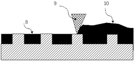
도 4는 마스타금형에 실버페이스트를 충진하는 것을 설명하는 설명도이다.
도 5는 기판과 경화된 실버페이스트를 접착제를 통하여 결합시키는 것을 설명하는 설명도이다.
도 6은 마스타금형으로부터 탈형시킨 회로기판을 설명한다.
도 7은 매립형 회로기판을 제작하는 것을 설명하는 설명도이다.
도 8은 매립형 회로기판의 연마공정을 설명하는 설명도이다.
도 9는 완전매립형 회로기판에 대한 설명도이다.
도 10, 도 11은은 개구부를 형성한 완전매립형 회로기판의 설명도이다.
도 12는 탈형을 용이하게 하기 위한 테이퍼 구조에 대한 설명도이다.
도 1은 모형금형에 대한 설명도이다.
본 발명에서는 모형금형은 마스타금형을 제작하기 위한 금형으로 정의한다.
본 발명에서 모형금형은 전주가공 또는 레이저 가공에 의하여 가공이 된다.
전주가공을 통하여 제작한다는 것은, 통전되는 기판에 포토리지스트를 도포한 하고, 상기 포토리지스트에 패턴을 통한 노광작업을 시행한다. 상기 노광작업 이후에는 현상공정을 거치며, 상기 현상공정 후에는 도금을 두텁게 실시한다.
상기 두터운 도금체를 기판으로부터 탈형하여 제작되어 얻어지는 것이 전주가공을 통하여 제작되는 모형금형이 된다.
모형금형의 표면은 오목부(2)와 볼록부(1)가 형성되어 진다.
초정밀한 미세회로를 구성하기 위하여서는 수 마이크로미터의 선폭을 갖는 오목부와 볼록부의 구성이 필수적이다.
상기 오목부와 볼록부에 의하여 미세한 회로가 구성이 되게 된다.
본 발명에서는 오목부와 볼록부의 크기를 조절하여, 초정밀한 회로부를 구성할 수가 있도록 한다. 회로부의 선폭의 크기는 1 마이크로미터에서 수 십 마이크로미터로 하며, 회로부의 깊이는 수 마이크로미터에서 수 십 마이크로미터에 이르도록 한다.
이러한 정밀한 오목부와 볼록부를 형성하기 위하여서는, 스테인레스 평판과 같은 도전성 평판에 포토리지스트를 균일하게 도포하고, 포토마스크를 사용하여 포토리지스트에 노광 및 현상을 하고, 현상 후 도금공정을 행하는 전주가공물을 만든다.
감광층의 두께가 회로부의 두께와 일치하게 된다.
이 전주가공물이 모형금형이 된다.
이때, 감광층을 노광시킴에 있어서, 감광층을 테이퍼 지게 노광을 시킴으로 전주가공물이 용이하게 탈형되도록 하는 것이 바람직하다.
전주가공물이 용이하게 탈형이 된다는 것은 이후의 마스타금형이 용이하게 탈형이 되는 것을 의미하며, 이는 후술할 경화되어진 실버페이스트의 탈형이 용이하다는 것을 의미한다.
이와같이 감광층을 테이퍼지게 노광을 시키는 것은 핵심기술의 하나이다. 이같이 테이퍼지게 노광을 시키는 것을 노광기의 기능에 달려져 있다.
테이퍼진 것에 대한 것은 도 12를 참고로 설명을 하겠다.
도전성 기판(31)에 포도리지스터(29)가 테이퍼 진 형상으로 노광이 되게 한다.
공간부는 역테이퍼(30)의 형상으로 구성된다.
도전체(33)에 전기를 통전시키어 도금을 실행하면, 공간부에 채워진 전주도금체(32)는 역테이퍼의 형상을 제작이 된다.
전주도금이 완성되면, 전주가공물(34)을 도전성 기판(35)으로부터 탈형을 시킨다. 이때, 테이퍼가 있음으로 인하여 탈형이 용이하게 된다.
본 발명에서는 이같이 탈형을 용이하게 하도록 테이퍼 진 오목부와 볼록부를 형성하는 것이 본 발명의 핵심기술의 하나로 한다.
본 발명에서는 이러한 테이퍼진 노광을 행하기 위하여 본 발명인이 발명한 렌티큐라를 이용한 선광원 노광기를 사용하면 용이하게 테어퍼진 노광을 시킬 수가 있다.
모형금형을 제작함에 있어서, 또다른 실시예로서는 레이저 가공을 들 수가 있다. 그러나 레이저 가공을 할 경우에는 테이퍼진 회로부를 제작하는 것이 용이하지 않다.
가공방법으로서는 레이저 가공을 통하여 수 마이크로미터의 회로부의 선폭을 가공할 수가 있는 것이다.
일반적으로 이러한 미세 정밀한 모형금형(3)은 도금에 의한 전주가공물이거나 금속기판에 레이저로 가공을 하는 것이 일반적이므로, 본 발명에서 모형금형은 금속금형이 된다.
도 2, 도 3은 마스타 금형의 설명도이다.
도 1에서 설명한 모형금형으로부터 복제되는 금형을 만들 수가 있다.
모형금형(6)에 액상의 수지를 부어서 마스타금형(4)를 제작할 수가 있다.
또는 모형금형에 필름 형태로 만들어진 수지 필름 또는 평판의 형태로 만들어진 수지판재에 열을 가열하여 프레스를 통하여 수지로 제작이 되는 마스타금형을 만들 수가 있다.
본 발명에서의 가장 대표적인 실시예로는, 전주가공에 의한 모형금형에 평판형태의 테프론 수지로 형성된 판재를 놓고, 가열 및 가압하여 성형한다.
성형이 마치면 냉각 후 탈형을 하게 되면, 정밀하게 모형금형의 형상을 복제한 마스타금형이 만들어 진다.
또 다른 실시예로서는 필름 형태의 테프론 수지를 사용하고, 상기 필름에는 평판의 형태를 유지하도록 하기 위하여, 금속판재 등의 보강재를 구성하여 가공을 할 수가 있다.
수지로 만드는 것 중에서 테프론 수지로 마스타금형을 만드는 이유로는 탈형의 용이함을 위한 이유가 가장 크다. 테프론 수지는 이형성이 탁월하여, 상기 테프론 수지로 만든 마스타금형에는 실버페이스트가 접착이 되지 못한다.
또한 상기 테프론 수지의 마스타금형에는 접착제로 사용되는 에폭시 수지가 접착력을 발휘할 수가 없다는 점을 본 발명에서 이용을 하는 것이다.
본 발명에서의 또다른 실시예로는 금속으로 구성되는 마스타금형을 사용할 수가 있다. 이 경우에는 상기 금속의 마스타 금형에 이형층을 형성하여야 한다.
이형층을 형성하기 위하여서는 이형제를 코팅하거나 이형물질을 도포하여야 한다.
본 발명에서는 모형금형으로부터 다수개의 마스타금형을 복제하여 제작을 할 수가 있다. 이 같이 모형금형으로부터 복제되어진 금형을 다수 개를 제작할 수가 있는데,
본 발명에서는 이를 마스타금형이라 칭한다.
모형금형(6)의 오목부가 마스타금형(4)의 볼록부(5)가 되며, 모형금형의 볼록부는 마스타금형의 오목부가 된다.
마스타금형을 사용하여 제품을 만들 경우, 금형으로부터 탈형이 되는 제품이 마스타금형으로부터 잘 떨어져 나오는 것이 중요하다.
이러한 탈형을 위하여서 마스타금형의 표면에 이형층을 형성하거나 이형을 위한 코팅을 통하여 탈형이 용이하게 할 수가 있다.
마스타금형을 만드는 소재는 금속이나 다양한 형태의 수지를 사용할 수가 있다.
본 발명의 실시예로서는 테프론 수지를 사용한 것을 들 수가 있다.
테프론 수지로 마스타금형을 제작하게 되면, 테프론 수지 금형 자체가 이형성이 뛰어나다. 이 경우에는 마스타금형에 이형층이나 이형을 위한 코팅이 필요가 없게 된다. 모형금형으로부터 탈형시킨 것이 도 3의 마스타금형(7)이 된다.
도 4는 마스타금형에 실버페이스트를 충진하는 것을 설명하는 설명도이다.
테프론 수지로 만든 마스타금형의 실시예를 중심으로 설명을 한다.
본 발명에서 사용이 되는 테프론수지 또는 불소수지에 대하여 상술한다.
테프론수지는 일반 플라스틱류보다 우수한 특성을 가지고 있으며, 일반 플라스틱에 비하여 내열성,내약품성,내저온성,전기절연성,고주파특성이 등이 매우 뛰어나며, 비점착성과 저마찰 특성도 갖추고 있다.
불소수지는 불소수지 원료를 사용하여 압축, 압출 성형하여 여러 종류의 소재 제작이 가능하다.
테프론 수지 표면 위에는 거의 모든 물질이 달라붙지 않는 특징이 있다.
불소수지의 융점은 제품 종류에 따라서 다르나 270도에서 327도 사이의 범주이다.
테프론은 -260도씨에서 +260도씨까지 사용할 수 있으며 단시간 사용의 경우 300도씨에서도 견디어 내며 TEFLON FEP는 232도씨에서 연속사용이 가능하다.
테프론 표면에는 물이나 기름이 잘 묻지 않는다. 따라서 표면이 오염되지 않을 뿐만 아니라 쉽게 청소할 수 있다. 테프론의 마찰계수는 일반적으로 속도, 부하에 따라 약간씩 차이가 있지만 약 0.5~0.20이다. 테프론은 일반적으로 모든 화학제품에 안정성을 보여준다. 테프론은 광역의 주파수내에서도 매우 높은 전기적 특성을 가지고 있다. 비절연성은 물론 우수한 표면 저항율을 갖는다. 극히 낮은 온도에서도 그 물리적 특징이 변하지 않고 유지된다. 테프론은 영하 260도씨의 낮은 온도에서도 사용된다.
본 발명에서의 테프론 수지로 만든 마스타 금형은 일반 금형에 테프론 코팅을 행한 것으로 용이하게 대체를 할 수가 있다. 따라서 본 발명의 테프론 수지 금형은 테프론코팅 금형이라는 단어로 대체가 가능하며, 이것 역시 본 발명의 청구대상으로 한다.
본 발명에서는 먼저, 테프론 수지로 만들어진 마스타금형의 오목부에 실버페이스트(8)를 충진한다.
스퀴즈(9)를 통하여 실버페이스트(10)는 마스타금형의 오목부에만 들어가게 한다.
테프론 수지로 만든 마스타 금형의 볼록부의 평면이 깨끗하고, 경면이 되어질수록 볼록부에 묻어 있는 실버페이스트의 제거는 용이하여 진다.
마스타 금형의 볼록부의 평면이 깨끗하고, 경면이 되면 스퀴즈로 한번 훑어 지나가더라도 볼록부의 평면에 묻은 실버페이스트는 깨끗하게 제거가 된다.
이것은 본 발명에 있어서 대단히 중요한 기술이 된다.
이형층이 형성된 마스타금형 또는 테프론 수지 마스타금형에서는, 마스타금형의 볼록부에 묻어진 실버페이스트는 스퀴즈에 의하여 용이하게 제거된다.
오목부에 충진된 실버페이스트는 가열하여 경화시킨다.
경화되어진 실버페이스트는 전기가 통하는 회로부의 역할을 하게 된다.
실버페이스트가 경화된 이후에, 마스타금형의 볼록수의 상부와 실버페이스트의 상부면을 연마한다.
불소수지의 마스타금형의 볼록부의 표면부에 스퀴즈로 정리된 실버페이스트가 조금은 미소하게 남아있을 수가 있다. 이같이 잔존되어진 미소의 실버페이스트는 경화되어진 후에는 볼록부의 표면부에 어떤 결합력이 없이 그냥 엊혀져 있는 상태가 된다.
이를 입도가 극히 미세한 연마제를 통하여 연마하여 제거한다. 이러한 연마를 통하여 불소수지의 마스타금형의 표면은 더욱 매끄러워 지게 된다.
경우에 따라서는 연마없이 작업을 진행시킬 수가 있다.
본 발명에서의 또다른 실시예로, 실버페이스트를 충진하지 않고, 스파트링에 의하여 금속층을 마스타금형의 오목부에 충진하는 것을 들 수가 있다.
물론 스파트링에 의하여 볼록부에도 금속층이 형성이 된다.
오목부에 금속층이 거의 다 충진되었을 때, 볼록부에 쌓여진 금속층은 제거한다.
이형성이 강한 테프론 수지 금형의 경우에는 볼록부에 쌓여진 금속층의 제거는 용이하다.
도 5는 기판과 경화된 실버페이스트를 접착제를 통하여 결합시키는 것을 설명하는 설명도이다.
기판은 경질기판, 투명기판, 불투명 기판, 에폭시 기판, 경질의 수지 기판, 필름, 투명 필름, 불투명 필름, 폴리이미드 필름, 투명 폴리이미드 필름, 불투명 폴리이미드 필름 등의 다양한 형태가 적용이 된다.
휘어지는 소재의 기판을 사용할 경우 FPCB 기판이 되는 것이다.
FPCB의 가장 대표적인 기판 소재는 폴리이미드 필름이 사용된다.
접합제 역시 다양한 것이 사용이 가능하다. 각종 접착성 수지, 유브이 수지, 폴리이미드 수지, 에폭시 수지 등이 사용되어진다.
제품에 필요한 특성에 따라서 접착제가 선택된다.
본 발명의 가장 대표적인 실시예로서는 에폭시 수지를 사용한다.
그 이유로는 공기가 통하는 않은 상태에서도 자체 경화가 일어나기 때문이다.
또한 잘 깨어지지 아니하고 접착력이 우수하기 때문이다.
만약 폴리이미드 수지를 사용하게 될 경우에는 방출되어지는 가스가 외부로 빠져 나가도록 하는 구조를 제공하여야만 폴리이미드 수지가 경화가 된다.
에폭시 수지는 폴리이미드 필름과 접착이 용이하며, 접착강도가 좋다.
또한 충격에도 강하며, 휨에도 견딜 수가 있다.
또한 에폭시 수지는 경화된 실버페이스트에도 접착성이 우수하다.
폴리이미드 필름(11)과, 경화된 실버페이스트가 충진된 마스타금형을, 에폭시 수지(13)에 의하여 접합을 시킨다.
액상의 에폭시 수지를 마스타금형의 표면에 균일하게 도포시키어 실시할 수가 있다.
액상의 에폭시 수지를 폴리이미드 필름에 균일하게 도포시키어 실시를 할 수도 있다.
이때, 균일한 에폭시 수지의 도포막을 형성하는 것이 바람직하다.
이를 위하여 롤러(12)를 사용하여 일정한 두께를 유지시킬 수가 있다.
스파트링에 의하여 오목부에 금속층이 쌓여지고, 볼록부에 쌓여진 금속층은 제거된 경우의 실시예에 대하여, 에폭시 수지를 통하여 폴리이이드 필름층에 결합을 시킬 수가 있음으로 물론이다.
도 6은 마스타금형으로부터 탈형시킨 회로기판을 설명한다.
에폭시 수지를 도포한 후, 가열하여 경화시킨다.
에폭시 수지(16)는 통기성이 전혀 없는 상태에서도 경화가 가능하다.
폴리이미드 수지를 접합제로 선택할 경우에는, 통기성이 전혀 없는 상태에서는 경화가 일어나지 않게 되므로, 먼저 적당한 온도에서 폴리이미드 수지를 경화를 시킨 후, 접합을 시킬 필요가 있다.
에폭시 수지(16)는 폴리이미드 필름(17)과의 결합도가 뛰어나다.
또한 에폭시 수지는 경화된 실버페이스트(15)와의 결합도도 뛰어나다.
에폭시 수지는 가장 용도가 넓은 플라스틱의 하나이며 접착제, 도료, 적층품, 주형품, 성형품등으로서 화학, 전기, 기계, 토목공업의 분야에서 다하고 있는 역할은 대단히 중요한 것이다.
에폭시는 반응성이 크기 때문에 경화제와 함께 사용한다. 에폭시 수지는 경화제에 반응해, 그 성질은 경화제의 종류나 배합비, 혹은 경화조건 등에 의해서 크게 달라진다. 에폭시 수지는 규소수지, 불소수지, 폴리에틸렌, 폴리프로필렌등을 제외하고는 무엇이든 접착할 수가 있다. 에폭시 수지 접착제는 액상, 페이스트상, 분말상, 봉상 등 여러 가지가 있으며, 액상이 가장 널리 사용되고 있다.
에폭시 수지는 동박의 접착에도 사용된다.
전자부품의 봉입성형(엔캡슐레이션)용으로 사용되기도 한다.
압축성형의 경우, 성형조건은 성형온도 140~160℃, 성형압력 100~200kgf/㎠, 경화시간 약 100~200sec/mm 이며, 성형후의 아프터 베이킹 함으로써 성형품의 성능은 더욱 향상된다.
이 성형재료는 경화 때에 휘발물질을 부생하지 않으므로 경화물의 치수변화가 적고 전기적 성질도 양호하다. 또한 유동성이 풍부하고 비교적 저압에서도 성형할 수 있으므로 복잡한 형상이나 인서트가 많은 성형품에 적합한 것이다.
치수안정성, 전기적 성능이 뛰어나기 때문에 주로 인서트가 많은 전기부품이나 치수정도가 요구되는 기계부품에 사용된다.
전자부품의 트랜스퍼 봉입성형에 일반화되고, 특히 반도체에 있어서는 그 대부분이 에폭시수지로 밀봉되고 있다.
에폭시 수지가 경화되어, 경화된 실버페이스트와 폴리이미드 필름이 접착이 된 이후에는 마스타금형으로부터 기판을 탈착시킨다.
마스타금형으로부터 탈착되어진 기판은 폴리이미드 필름에 회로부가 구성된 회로기판이 된다. 회로부와 회로부 사이에는 공간부(14)가 존재한다.
이형층이 형성된 마스타금형 또는 테프론 수지로 만들어진 마스타금형은 이형성이 탁월하므로 탈형이 용이하다.
폴리이미드 필름을 사용하고, 에폭시 수지를 접착제로 사용한 경우, 탈형 되어진 회로기판은 폴리이미드 FPCB가 된다.
본 발명에서는 회로의 선폭이 수 마이크로미터의 초정밀한 회로의 구성이 얼마든지 가능하다.
본 발명의 방법으로 제작된 폴리이미드 회로기판은 평판도를 유지할 수가 있는 특징이 있다.
폴리이미드 필름은 잘 휘어지며, 환경에 따라서 컬현상이 발생한다.
컬현상이란 말리는 현상을 설명한다.
폴리이미드 필름에 결합되는 에폭시와 경화된 실버페이스트 또는 스파트링에 의하여 형성된 금속층은 폴리이미드 필름이 평탄도를 유지하도록 하는 데 기여를 한다.
본 발명에서의 폴리이미드 회로기판은 컬현상이 없으므로 적층하여 다층의 기판을 제작
도 7은 매립형 회로기판을 제작하는 것을 설명하는 설명도이다.
폴리이미드 필름은 높은 열 안정성 및 효과적인 기계적 특성을 가진다. 폴리이미드(PI) 필름은 영상 400도 이상의 고온이나 영하 269도의 저온을 견디며, 얇고 굴곡성이 뛰어난 첨단 고기능성 산업용 소재이다.
내화학성, 내마모성도 강해 열악한 환경에서 안정적인 성능 유지가 필요한 분야에 널리 쓰인다. 주로 연성회로기판(FPCB)의 원판에 사용된다.
폴리이미드는 내열성 고분자로, 기계적 강도가 높고 충격에 강하며 치수안정성이 좋다. 전기절연성과 내마모성, 내약품성도 좋다. 또한 난연성이다. 단점은 대부분 열경화성으로 성형성이 나쁘다.
전자기기의 소형화 및 고집적화에 따라 필름 형태의 폴리이미드가 FPC의 용도에서 크게 각광받는 소재가 되었다.
폴리이미드 필름은 COF(Chip On Flexible Printed Circuit 혹은 Chip On Film 등으로 발전하여, 단순히 구부릴 수 있는 전기도선 역할 뿐 아니라 부품의 표면실장이 가능한 정도의 치수안정성과 기계적 물성을 가진다.
동박적층 폴리이미드필름은 내열 난연성 에폭시계 접착제를 사용하여 폴리이미드 필름과 동박을 적층시킨 연성회로기판(FPCB)용 재료이다. 탁월한 내열성과 내화학성, 그리고 우수한 전기적, 기계적 특성을 모두 지니고 있어 휴대폰, 디지털 카메라등의 고기능성, 소형화, 경량화가 요구되는 제품에 매우 적합한 재료이다.
본 발명에서 탈형되어진 폴리이미드 회로기판에서, 회로부와 이웃하는 회로부의 사이에는 공간부(14)가 형성되어져 있다.
이러한 공간부를 비전도성의 수지로 매립하게 되면 더욱 회로부가 기판에 견고히 부착을 하게 된다.
이러한 목적을 위하여, 실시예로서, 공간부에 에폭시 수지를 충진하고, 충진된 에폭시 수지(18)를 경화를 시킨다.
본 발명에서는 회로부의 측면은 매립이 되고, 표면은 노출된 상태를 매립형 회로기판이라 정의한다.
충진되어지는 비도전성 수지는 액상의 폴리이미드 수지를 사용할 수도 있다.
액상의 폴리이미드 수지가 공기중에서 가열에 의하여 경화가 용이하기 때문이다.
도 8은 매립형 회로기판의 연마공정을 설명하는 설명도이다.
에폭시 수지가 경화 된 후, 회로기판의 표면을 미세연마기(19)를 통하여 깨끗하게 정리를 한다.
도 9는 완전매립형 회로기판에 대한 설명도이다.
탈형되어진 폴리이미드 회로기판은, 폴리이미드필름(23)에 경화된 회로부(21)가 에폭시 수지층(22)에 결합된 상태이다.
이때, 회로부와 이웃하는 회로부의 사이에는 공간부가 형성되어져 있다.
이러한 공간부를 포함한 회로부의 상부 전체를 비전도성의 수지(20)로 덮으면 회로부가 기판에 견고히 부착을 하게 될 뿐만 아니라, 회로가 절연 된다.
실시예로서, 비전도성 수지는 에폭시 수지를 사용한다. 물론 비전도성 수지는 폴리이미드 수지도 사용을 할 수가 있다.
본 발명에서는 회로부의 측면과 회로부의 표면까지 완전히 매립된 회로기판을 완전매립형 회로기판이라 정의한다.
도 10, 도 11은은 개구부를 형성한 완전매립형 회로기판의 설명도이다.
도 11에서와 같이 완전매립형 회로기판에서 상부의 일부를 절개하여 개구부를 형성시킨 것을 개구부를 형성한 완전매립형 회로기판이라 정의한다.
이같이 개구부를 형성하여 일부의 회로부를 노출시키어, 노출된 회로부에 전기적 연결을 할 수가 있도록 하기 위한 것이다.
이를 제작하기 위하여서는 먼저, 도 10과 같이 제작공정이 필요하다.
먼저 도 7에서와 같이 매립형 회로기판의 일부에 덮개(25)를 구성한다.
덮개는 접착테이프 등과 같은 소재를 사용할 수가 있다.
또한 덮개를 형성하기 위하여, 감광재를 사용할 수도 있다.
이를 위하여 먼저 매립형 회로기판의 상부에 감광재를 도포한다.
상기 감광재에 노광 및 현상공정을 통하여 필요한 부위만 감광재를 남기어 정밀하게 덮개를 제작할 수가 있다. 감광재를 사용하여 덮개를 형성한 경우, 덮개의 제거도 용이하게 된다. 즉 화학적으로 처리하여 쉽게 덮개의 제거가 가능하게 된다.
덮개(25)를 형성 후, 매립형회로기판의 상부에 비도전성 수지(24)를 도포하고, 경화시킨다.
비도전성 수지(24)의 하부에는 회로부(26) 사이 사이에 에폭시 수지(27)가 충진된 상태이다.
상기 비도전성 수지는 액상의 에폭시 수지로 할 수가 있다.
또는 액상의 폴리이미드 수지를 사용할 수가 있다.
비도전성 수지가 경화된 후에, 덮개(25)를 제거한다.
덮개가 제거된 부분은 도 11에서와 같이 회로부(28)가 노출된다.
노출된 회로부(28)는 전기적으로 다른 회로에 연결을 시킬 수가 있다.
도 12는 탈형을 용이하게 하기 위한 테이퍼 구조에 대한 설명도이다.
전주가공물을 통하여 금형을 제작할 때, 포토리지스트에 대하여 테이퍼진 노광작업을 실시하여 제작을 시작한다.
도전체 평판(31) 위에 포토리리스트(29)를 노광시키어, 테이퍼 진 구조로 노광과 현상을 진행한다.
테이퍼 진 포토리지스트(29)와 테이퍼 진 공간부(30)가 형성된다.
도전체 평판(33)에 전기를 연결하여 도금을 시작하면 전주가공물(32)가 형성된다.
전주가공물(34)을 도전체 평판(35)로부터 탈형시키면 탈형이 용이한 금형이 만들어 진다.
본 발명은 미세회로를 가지는 플렉시블 회로기판의 제작방법과 그 방법으로 만들어진 미세회로를 가지는 플렉시블 회로기판을 포함한다.
본 발명은 통전회로로 구성되는 회로부가 에폭시 수지에 의하여 폴리이드미 필름기판에 결합된 것을 특징으로 하는 미세회로를 가지는 플렉시블 회로기판과 그 제작방법을 포함한다.
또한 본 발명은 회로기판이 매립형 또는 완전매립형으로 구성된 것도 포함한다.
본 발명은, 본 발명에 속하는 기술 분야에서 통상의 지식을 가진 자가 본 발명의 기술적 사상을 벗어나지 않는 범위 내에서 여러 가지 치환 변형이 가능하므로, 본 발명은 전술한 실시예 및 첨부된 도면에만 한정되는 것은 아니다.
[부호의 설명]
1: 볼록부 2: 오목부 3: 모형금형 4: 마스타금형
5: 볼록부 6: 모형금형 7: 마스타금형 8: 실버페이스트
9: 스퀴즈 10: 실버페이스트 11: 폴리이미드 필름
12: 롤러 13: 에폭시 수지 14: 공간부
15: 경화된 실버페이스트 16: 에폭시 수지 17: 폴리이미드 필름
18: 충진된 에폭시 수지 19: 미세연마기 20: 비전도성의 수지
21: 회로부 22: 에폭시 수지층 23: 폴리이미드필름
24: 비도전성 수지 25: 덮개 26: 회로부 27: 에폭시 수지
28: 회로부
Claims (18)
- 오목부와 볼록부를 통하여 미세회로가 형성된 전주금형으로부터, 오목부와 볼록부를 통하여 미세회로가 형성된 마스타금형을 제작하고;상기 마스타금형의 오목부에 실버페이스트를 충진하고, 가열장치를 통하여 상기 실버페이스를 경화시키며;마스타금형의 볼록부의 표면부와 경화된 실버페이스트의 노출 표면부에 에폭시 수지를 도포하며;상기 에폭시 수지를 통하여 폴리이미드 필름을 접합시키고, 에폭시 수지를 경화시킨 후;마스타금형을 탈형시키는 것을 특징으로 하는 미세회로를 가지는 플렉시블 회로기판의 제작방법.
- 제 1항에 있어서, 상기 마스타 금형은 테프론 수지로 제작되는 것을 특징으로 하는 미세회로를 가지는 플렉시블 회로기판의 제작방법.
- 제 1항에 있어서, 마스타 금형은 금속 또는 수지로서 제작되는 것을 특징으로 하는 미세회로를 가지는 플렉시블 회로기판의 제작방법.
- 제 3항에 있어서, 금형의 표면에 이형층을 형성하여 사용하는 것을 특징으로 하는 미세회로를 가지는 플렉시블 회로기판의 제작방법.
- 제 1항에서 제 4항의 어느 한 항에 있어서, 에폭시 수지를 대신하여 폴리이미드 수지 또는 유브이 수지 액상수지로 사용하는 것을 특징으로 하는 미세회로를 가지는 플렉시블 회로기판의 제작방법.
- 제 1항에서 제 6항의 어느 한 항에 의하여 제작된 것을 특징으로 하는 미세회로를 가지는 플렉시블 회로기판.
- 통전회로로 구성되는 경화된 실버페이스트가 에폭시 수지에 의하여 폴리이드미 필름기판에 결합된 것을 특징으로 하는 미세회로를 가지는 플렉시블 회로기판.
- 제 7항에 있어서, 실버페이스트가 매립형으로 구성된 것을 특징으로 하는 미세회로를 가지는 플렉시블 회로기판.
- 제 7항에 있어서, 실버페이스트가 완전매립형으로 구성된 것을 특징으로 하는 미세회로를 가지는 플렉시블 회로기판.
- 오목부와 볼록부를 통하여 미세회로가 형성된 전주금형으로부터, 오목부와 볼록부를 통하여 미세회로가 형성된 마스타 금형을 제작하고;상기 마스타 금형의 오목부에 스파터링에 의하여 금속층을 형성하고;마스타 금형의 볼록부의 표면부와 오목부의 스파터링 금속층에 에폭시 수지를 도포하며;상기 에폭시 수지를 통하여 폴리이미드 필름을 접합시키고, 에폭시 수지를 경화시킨 후;마스타 금형을 탈형시키는 것을 특징으로 하는 미세회로를 가지는 플렉시블 회로기판의 제작방법.
- 제 10항에 있어서, 상기 마스타 금형은 테프론 수지로 제작되는 것을 특징으로 하는 미세회로를 가지는 플렉시블 회로기판의 제작방법.
- 제 10항에 있어서, 마스타 금형은 금속 또는 수지로서 제작되는 것을 특징으로 하는 미세회로를 가지는 플렉시블 회로기판의 제작방법.
- 제 12항에 있어서, 금형의 표면에 이형층을 형성하여 사용하는 것을 특징으로 하는 미세회로를 가지는 플렉시블 회로기판의 제작방법.
- 제 10항에서 제 13항의 어느 한 항에 있어서, 에폭시 수지를 대신하여 폴리이미드 수지 또는 유브이 수지 액상수지로 사용하는 것을 특징으로 하는 미세회로를 가지는 플렉시블 회로기판의 제작방법.
- 제 10항에서 제 14항의 어느 한 항에 의하여 제작된 것을 특징으로 하는 미세회로를 가지는 플렉시블 회로기판.
- 마스타금형의 오목부에 통전회로로 구성되는 스파트링에 의한 금속층이, 에폭시 수지에 의하여 폴리이드미 필름기판에 결합된 것을 특징으로 하는 미세회로를 가지는 플렉시블 회로기판.
- 제 16항에 있어서, 스파터링 금속층이 매립형으로 구성된 것을 특징으로 하는 미세회로를 가지는 플렉시블 회로기판.
- 제 16항에 있어서, 스파터링 금속층이 완전매립형으로 구성된 것을 특징으로 하는 미세회로를 가지는 플렉시블 회로기판.
Applications Claiming Priority (2)
| Application Number | Priority Date | Filing Date | Title |
|---|---|---|---|
| KR10-2015-0027219 | 2015-02-26 | ||
| KR1020150027219A KR20160104346A (ko) | 2015-02-26 | 2015-02-26 | 마스타금형에서 탈형시키는 것을 특징으로 하는 미세회로를 가지는 플렉시블 회로기판의 제작방법과 그 제품 |
Publications (1)
| Publication Number | Publication Date |
|---|---|
| WO2016137264A1 true WO2016137264A1 (ko) | 2016-09-01 |
Family
ID=56789734
Family Applications (1)
| Application Number | Title | Priority Date | Filing Date |
|---|---|---|---|
| PCT/KR2016/001908 Ceased WO2016137264A1 (ko) | 2015-02-26 | 2016-02-26 | 마스타금형에서 탈형시키는 것을 특징으로 하는 미세회로를 가지는 플렉시블 회로기판의 제작방법과 그 제품 |
Country Status (2)
| Country | Link |
|---|---|
| KR (1) | KR20160104346A (ko) |
| WO (1) | WO2016137264A1 (ko) |
Cited By (2)
| Publication number | Priority date | Publication date | Assignee | Title |
|---|---|---|---|---|
| CN111712054A (zh) * | 2020-07-29 | 2020-09-25 | 欣强电子(清远)有限公司 | 一种软板覆盖膜快速贴合方法 |
| CN113990760A (zh) * | 2021-10-26 | 2022-01-28 | 苏州链芯半导体科技有限公司 | 一种改进性的柔性无芯3d印刷集成电路模压工艺 |
Families Citing this family (1)
| Publication number | Priority date | Publication date | Assignee | Title |
|---|---|---|---|---|
| WO2018131960A1 (ko) * | 2017-01-13 | 2018-07-19 | 성낙훈 | 전주가공법에 의하여 제작되는 금형과 그 제작방법 |
Citations (5)
| Publication number | Priority date | Publication date | Assignee | Title |
|---|---|---|---|---|
| KR101118987B1 (ko) * | 2009-09-11 | 2012-03-12 | (주)티에스티아이테크 | 광학부재의 제조 방법 |
| US20130233605A1 (en) * | 2012-03-12 | 2013-09-12 | Industrial Technology Research Institute | Solid electrolytic capacitor and circuit board having the same |
| KR101361171B1 (ko) * | 2012-11-02 | 2014-02-10 | 주식회사 엔엔피 | 기판 제조 방법 |
| KR20140037635A (ko) * | 2012-09-19 | 2014-03-27 | 성낙훈 | 도전성 페이스트를 충진시켜서 회로기판을 제작하는 방법과 그 방법에 의하여 제작된 회로기판 |
| KR20140094131A (ko) * | 2013-01-21 | 2014-07-30 | 성낙훈 | 음각부에 실버페이스트를 충진시켜 극미세 도전성 회로부를 구성하는 기판의 제조방법과 그에 의한 기판. |
-
2015
- 2015-02-26 KR KR1020150027219A patent/KR20160104346A/ko not_active Withdrawn
-
2016
- 2016-02-26 WO PCT/KR2016/001908 patent/WO2016137264A1/ko not_active Ceased
Patent Citations (5)
| Publication number | Priority date | Publication date | Assignee | Title |
|---|---|---|---|---|
| KR101118987B1 (ko) * | 2009-09-11 | 2012-03-12 | (주)티에스티아이테크 | 광학부재의 제조 방법 |
| US20130233605A1 (en) * | 2012-03-12 | 2013-09-12 | Industrial Technology Research Institute | Solid electrolytic capacitor and circuit board having the same |
| KR20140037635A (ko) * | 2012-09-19 | 2014-03-27 | 성낙훈 | 도전성 페이스트를 충진시켜서 회로기판을 제작하는 방법과 그 방법에 의하여 제작된 회로기판 |
| KR101361171B1 (ko) * | 2012-11-02 | 2014-02-10 | 주식회사 엔엔피 | 기판 제조 방법 |
| KR20140094131A (ko) * | 2013-01-21 | 2014-07-30 | 성낙훈 | 음각부에 실버페이스트를 충진시켜 극미세 도전성 회로부를 구성하는 기판의 제조방법과 그에 의한 기판. |
Cited By (3)
| Publication number | Priority date | Publication date | Assignee | Title |
|---|---|---|---|---|
| CN111712054A (zh) * | 2020-07-29 | 2020-09-25 | 欣强电子(清远)有限公司 | 一种软板覆盖膜快速贴合方法 |
| CN111712054B (zh) * | 2020-07-29 | 2021-09-28 | 欣强电子(清远)有限公司 | 一种软板覆盖膜快速贴合方法 |
| CN113990760A (zh) * | 2021-10-26 | 2022-01-28 | 苏州链芯半导体科技有限公司 | 一种改进性的柔性无芯3d印刷集成电路模压工艺 |
Also Published As
| Publication number | Publication date |
|---|---|
| KR20160104346A (ko) | 2016-09-05 |
Similar Documents
| Publication | Publication Date | Title |
|---|---|---|
| WO2015106480A1 (zh) | 电磁波屏蔽膜以及包含屏蔽膜的线路板的制作方法 | |
| WO2014137192A2 (ko) | 금속 세선을 포함하는 투명 기판 및 그 제조 방법 | |
| WO2015072775A1 (ko) | 연성인쇄회로기판과 그 제조 방법 | |
| WO2015122721A1 (ko) | 마스터 몰드의 제조방법, 이로 제조된 마스터 몰드, 투명포토마스크의 제조방법, 이로 제조된 투명포토마스크 및 상기 투명포토마스크를 이용한 전도성 메쉬패턴의 제조방법 | |
| WO2015026026A1 (ko) | 프로세스 모듈 및 그 제조 방법과, 프로세스 모듈을 이용한 기판 처리 방법 | |
| WO2012087059A2 (en) | Printed circuit board and method for manufacturing the same | |
| WO2012087058A2 (en) | Printed circuit board and method for manufacturing the same | |
| WO2014178639A1 (ko) | 연성인쇄회로기판 및 그 제조 방법 | |
| WO2021080305A1 (ko) | 인쇄회로기판 | |
| WO2018147678A1 (ko) | 시드층을 이용한 회로형성방법 및 시드층의 선택적 에칭을 위한 에칭액 조성물 | |
| WO2018044053A1 (ko) | 연성인쇄회로기판 제조 방법 및 이에 의해 제조된 연성인쇄회로기판 | |
| WO2012087060A2 (en) | Printed circuit board and method for manufacturing the same | |
| WO2018221876A1 (ko) | 연성인쇄회로기판 제조 방법 및 이에 의해 제조된 연성인쇄회로기판 | |
| WO2020180145A1 (ko) | 패키징 기판 및 이를 포함하는 반도체 장치 | |
| KR20160092686A (ko) | 전도성 유동성 소재로 성형된 미세회로를 접착제를 사용하여 기판에 접합시킨 반도체 기판과 그 제조방법 | |
| KR20160104346A (ko) | 마스타금형에서 탈형시키는 것을 특징으로 하는 미세회로를 가지는 플렉시블 회로기판의 제작방법과 그 제품 | |
| EP2856501A1 (en) | Semiconductor package substrate, package system using the same and method for manufacturing thereof | |
| KR102412346B1 (ko) | 미세회로 기판과 그 제조방법 | |
| WO2019107819A1 (ko) | 인쇄회로기판 제조방법 | |
| WO2015076465A1 (ko) | 금속 박판을 적층한 반도체 검사 패드 및 제조방법 | |
| JP2016176090A (ja) | 電鋳型、電鋳母型及び電鋳母型の製造方法 | |
| WO2014129852A1 (ko) | 터치패널센서 및 그 제조방법 | |
| WO2014025144A1 (ko) | 시료보관기구의 제조방법 및 시료보관기구 | |
| WO2015099451A1 (ko) | 연성 인쇄회로기판 형성용 절연 수지 시트 및 이의 제조방법, 이를 포함하는 인쇄회로기판 | |
| WO2018131960A1 (ko) | 전주가공법에 의하여 제작되는 금형과 그 제작방법 |
Legal Events
| Date | Code | Title | Description |
|---|---|---|---|
| 121 | Ep: the epo has been informed by wipo that ep was designated in this application |
Ref document number: 16755914 Country of ref document: EP Kind code of ref document: A1 |
|
| NENP | Non-entry into the national phase |
Ref country code: DE |
|
| 32PN | Ep: public notification in the ep bulletin as address of the adressee cannot be established |
Free format text: NOTING OF LOSS OF RIGHTS PURSUANT TO RULE 112(1) EPC (EPO FORM 1205A DATED 16.01.2018) |
|
| 122 | Ep: pct application non-entry in european phase |
Ref document number: 16755914 Country of ref document: EP Kind code of ref document: A1 |