WO2016136502A1 - 固体撮像素子、および電子装置 - Google Patents
固体撮像素子、および電子装置 Download PDFInfo
- Publication number
- WO2016136502A1 WO2016136502A1 PCT/JP2016/054145 JP2016054145W WO2016136502A1 WO 2016136502 A1 WO2016136502 A1 WO 2016136502A1 JP 2016054145 W JP2016054145 W JP 2016054145W WO 2016136502 A1 WO2016136502 A1 WO 2016136502A1
- Authority
- WO
- WIPO (PCT)
- Prior art keywords
- light
- photoelectric conversion
- wavelength
- solid
- conversion unit
- Prior art date
- Legal status (The legal status is an assumption and is not a legal conclusion. Google has not performed a legal analysis and makes no representation as to the accuracy of the status listed.)
- Ceased
Links
Images











Classifications
-
- H—ELECTRICITY
- H10—SEMICONDUCTOR DEVICES; ELECTRIC SOLID-STATE DEVICES NOT OTHERWISE PROVIDED FOR
- H10F—INORGANIC SEMICONDUCTOR DEVICES SENSITIVE TO INFRARED RADIATION, LIGHT, ELECTROMAGNETIC RADIATION OF SHORTER WAVELENGTH OR CORPUSCULAR RADIATION
- H10F39/00—Integrated devices, or assemblies of multiple devices, comprising at least one element covered by group H10F30/00, e.g. radiation detectors comprising photodiode arrays
- H10F39/10—Integrated devices
- H10F39/12—Image sensors
-
- B—PERFORMING OPERATIONS; TRANSPORTING
- B82—NANOTECHNOLOGY
- B82Y—SPECIFIC USES OR APPLICATIONS OF NANOSTRUCTURES; MEASUREMENT OR ANALYSIS OF NANOSTRUCTURES; MANUFACTURE OR TREATMENT OF NANOSTRUCTURES
- B82Y15/00—Nanotechnology for interacting, sensing or actuating, e.g. quantum dots as markers in protein assays or molecular motors
-
- H—ELECTRICITY
- H10—SEMICONDUCTOR DEVICES; ELECTRIC SOLID-STATE DEVICES NOT OTHERWISE PROVIDED FOR
- H10F—INORGANIC SEMICONDUCTOR DEVICES SENSITIVE TO INFRARED RADIATION, LIGHT, ELECTROMAGNETIC RADIATION OF SHORTER WAVELENGTH OR CORPUSCULAR RADIATION
- H10F39/00—Integrated devices, or assemblies of multiple devices, comprising at least one element covered by group H10F30/00, e.g. radiation detectors comprising photodiode arrays
- H10F39/10—Integrated devices
- H10F39/12—Image sensors
- H10F39/18—Complementary metal-oxide-semiconductor [CMOS] image sensors; Photodiode array image sensors
- H10F39/182—Colour image sensors
- H10F39/1825—Multicolour image sensors having stacked structure, e.g. NPN, NPNPN or multiple quantum well [MQW] structures
-
- H—ELECTRICITY
- H10—SEMICONDUCTOR DEVICES; ELECTRIC SOLID-STATE DEVICES NOT OTHERWISE PROVIDED FOR
- H10F—INORGANIC SEMICONDUCTOR DEVICES SENSITIVE TO INFRARED RADIATION, LIGHT, ELECTROMAGNETIC RADIATION OF SHORTER WAVELENGTH OR CORPUSCULAR RADIATION
- H10F39/00—Integrated devices, or assemblies of multiple devices, comprising at least one element covered by group H10F30/00, e.g. radiation detectors comprising photodiode arrays
- H10F39/80—Constructional details of image sensors
- H10F39/805—Coatings
- H10F39/8053—Colour filters
-
- H—ELECTRICITY
- H10—SEMICONDUCTOR DEVICES; ELECTRIC SOLID-STATE DEVICES NOT OTHERWISE PROVIDED FOR
- H10F—INORGANIC SEMICONDUCTOR DEVICES SENSITIVE TO INFRARED RADIATION, LIGHT, ELECTROMAGNETIC RADIATION OF SHORTER WAVELENGTH OR CORPUSCULAR RADIATION
- H10F39/00—Integrated devices, or assemblies of multiple devices, comprising at least one element covered by group H10F30/00, e.g. radiation detectors comprising photodiode arrays
- H10F39/80—Constructional details of image sensors
- H10F39/806—Optical elements or arrangements associated with the image sensors
-
- H—ELECTRICITY
- H10—SEMICONDUCTOR DEVICES; ELECTRIC SOLID-STATE DEVICES NOT OTHERWISE PROVIDED FOR
- H10K—ORGANIC ELECTRIC SOLID-STATE DEVICES
- H10K39/00—Integrated devices, or assemblies of multiple devices, comprising at least one organic radiation-sensitive element covered by group H10K30/00
- H10K39/30—Devices controlled by radiation
- H10K39/32—Organic image sensors
-
- H—ELECTRICITY
- H10—SEMICONDUCTOR DEVICES; ELECTRIC SOLID-STATE DEVICES NOT OTHERWISE PROVIDED FOR
- H10F—INORGANIC SEMICONDUCTOR DEVICES SENSITIVE TO INFRARED RADIATION, LIGHT, ELECTROMAGNETIC RADIATION OF SHORTER WAVELENGTH OR CORPUSCULAR RADIATION
- H10F39/00—Integrated devices, or assemblies of multiple devices, comprising at least one element covered by group H10F30/00, e.g. radiation detectors comprising photodiode arrays
- H10F39/80—Constructional details of image sensors
- H10F39/806—Optical elements or arrangements associated with the image sensors
- H10F39/8063—Microlenses
Definitions
- the present disclosure relates to a solid-state imaging device and an electronic device, and more particularly, to a solid-state imaging device and an electronic device suitable for use when each pixel has a vertical spectral structure.
- each pixel in a solid-state imaging device has been provided with a color filter colored in different colors such as R, G, and B for each pixel, and a PD (photograph) is provided according to incident light input through the color filter.
- a photoelectric conversion unit including a diode generates electric charges by photoelectric conversion.
- each pixel outputs a monochrome pixel signal corresponding to the color of the color filter.
- each pixel region of the solid-state imaging device has a vertical spectral configuration in which organic photoelectric conversion films and a plurality of PDs are stacked in the vertical direction so that each pixel can output pixel signals of a plurality of colors simultaneously.
- a solid-state image sensor has been proposed (see, for example, Patent Document 1).
- FIG. 1 is a cross-sectional view showing an example of a solid-state imaging device having a longitudinal spectral configuration.
- the solid-state imaging device has an organic photoelectric conversion film 1 having a selective sensitivity to a G (Green) component of incident light and a selective sensitivity to a B (Blue) component in order from the light incident side.
- a second PD (R-PD) 3 having a selective sensitivity to the R (Red) component.
- the G component of the incident light is absorbed by the organic photoelectric conversion film 1
- the B component is absorbed by the first PD 2
- the R component is absorbed by the second PD 3 and converted into electric charge.
- the R component passes through the first PD 2 and enters the second PD 3, or the B component that cannot be absorbed (converted) by the first PD 2 is incident on the second PD 3. Due to the structure shown in Fig. 1, color mixing cannot be avoided. Such a color mixture causes a lack of sensitivity at the same time. This problem will be described with reference to FIG.
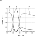
- FIG. 2 shows the spectral sensitivity characteristics of the solid-state imaging device shown in FIG. That is, the curve G in the figure shows the spectral sensitivity of the organic photoelectric conversion film 1, the curve B shows the spectral sensitivity of the first PD2, and the curve R shows the spectral sensitivity of the second PD3.
- the first PD 2 absorbs the R component (around 550 to 700 nm) in addition to the B component that should be absorbed originally.
- the second PD 3 absorbs the B component (around 400 to 550 nm) in addition to the R component that should be absorbed originally.
- the matrix coefficient at the time of the color correction calculation increases, and as a result, the image quality deterioration (SN ratio deterioration) is caused by the color correction calculation. .
- the present disclosure has been made in view of such circumstances, and is intended to suppress color mixing and sensitivity reduction in each pixel of a solid-state imaging device having a longitudinal spectral structure.
- the solid-state imaging device is a solid-state imaging device including a vertical-direction spectral structure pixel in which a plurality of photoelectric conversion units are stacked, and the vertical-direction spectral structure pixel is a first of the incident light.
- a first photoelectric conversion unit that generates a charge in response to light of a second wavelength and a second photoelectric component that generates a charge in response to light of a second wavelength among the incident light that has passed through the first photoelectric conversion unit
- a first spectroscopic unit that is formed on the upper surface of the first photoelectric conversion unit and that bends the traveling direction of the light of the first wavelength of the incident light in a lateral direction.
- the first spectroscopic unit can bend the traveling direction of the light having the first wavelength of the incident light in the extending direction of the first photoelectric conversion unit.
- the first beam splitting unit can go straight without changing the traveling direction of light other than the first wavelength of the incident light.
- the first spectroscopic unit may be a diffraction grating.
- the first spectroscopic unit may be a metal nanoparticle or a metal nanowire.
- the thickness of the layer of the first photoelectric conversion unit can be made thinner than the operation thickness of the second photoelectric conversion unit.
- the vertical spectral structure pixel may further include a third photoelectric conversion unit that generates an electric charge in response to light having a third wavelength of incident light, and the first photoelectric conversion unit includes the first photoelectric conversion unit. 3, a charge is generated in response to the light having the first wavelength whose traveling direction is bent by the first spectroscopic unit, and the second photoelectric conversion unit An electric charge can be generated according to light of the second wavelength among the incident light transmitted through the photoelectric conversion unit, the first spectroscopic unit, and the first photoelectric conversion unit.
- the first and second photoelectric conversion units can be PDs, and the third photoelectric conversion unit can be an organic photoelectric conversion film.
- the solid-state imaging device further includes a non-longitudinal direction spectral structure pixel including a third photoelectric conversion unit that generates charges in response to light having a third wavelength of incident light. Can do.
- the first to third photoelectric conversion units can be PDs.
- the non-vertical direction spectral structure pixel may further include a color filter that transmits only light of the third wavelength on an upper surface of the third photoelectric conversion unit.
- a color filter that transmits only light of the first and second wavelengths can be further provided on the upper surface of the spectroscopic unit.
- the vertical spectral structure pixel includes a third photoelectric conversion unit that generates charges in response to light having a third wavelength of incident light, and the input surface formed on an upper surface of the third photoelectric conversion unit.
- a second spectroscopic unit that bends the traveling direction of the light having the third wavelength in the lateral direction, and the third photoelectric conversion unit includes the first spectroscopic unit and the first spectroscopic unit.
- a charge is generated in response to the light having the third wavelength among the incident light transmitted through the photoelectric conversion unit, and the second photoelectric conversion unit is configured to include the first spectroscopic unit and the first photoelectric conversion unit. Charges can be generated in response to light of the second wavelength of the incident light transmitted through the first, second spectroscopic, and third photoelectric conversion units.
- the second spectroscopic unit may be a diffraction grating, a metal nanoparticle, or a metal nanowire.
- the first to third photoelectric conversion units can be PDs.
- the vertical direction spectral structure pixel may further include a condensing unit for condensing the incident light near the center of the vertical direction spectral structure pixel.
- the light of the first wavelength can be B component light
- the light of the second wavelength can be R component light
- the light of the third wavelength can be G component light
- An electronic device is an electronic device including a solid-state imaging device including a vertical spectral structure pixel in which a plurality of photoelectric conversion units are stacked, and the vertical spectral structure pixel includes incident light.
- a first photoelectric conversion unit that generates a charge in response to light having a first wavelength, and a charge that corresponds to light having a second wavelength in the incident light transmitted through the first photoelectric conversion unit.
- a second photoelectric conversion unit that generates light, and a first spectroscopic unit that is formed on an upper surface of the first photoelectric conversion unit and that bends the traveling direction of the light having the first wavelength of the incident light in a lateral direction.
- the traveling direction of the light having the first wavelength of incident light is bent in the lateral direction, and the light is transmitted in accordance with the light having the first wavelength. Charge is generated.
- color mixing and sensitivity reduction in each pixel can be suppressed.
- FIG. 1 It is sectional drawing which shows an example of a structure of the solid-state image sensor which has the conventional longitudinal direction spectral structure. It is a figure which shows the spectral sensitivity characteristic of the solid-state image sensor shown by FIG. It is a schematic sectional drawing of the solid-state image sensor which has the vertical direction spectral structure to which this indication is applied. It is a figure which shows the spectral sensitivity characteristic which can be anticipated with respect to the solid-state image sensor shown by FIG. It is a figure for demonstrating the diffraction conditions of a diffraction grating. It is a figure which shows the structure of the solid-state image sensor employ
- FIG. 3 is a schematic cross-sectional view of a solid-state imaging device having a longitudinal spectral structure to which the present disclosure is applied.
- This solid-state imaging device is configured by sequentially stacking the diffraction grating 11, the first PD 12, and the second PD 13 in the vertical direction from the light incident surface side.
- an on-chip lens that collects incident light near the center of the pixel is formed on the upper surface side of the diffraction grating 11, and between the diffraction grating 11 and the on-chip lens.
- the diffraction grating 11 diffracts light of a predetermined wavelength corresponding to the arrangement period w of the scatterers constituting the diffraction grating 11 in the horizontal direction (lateral direction) out of the incident light. Light of other wavelengths is transmitted without being diffracted.
- the period w is set so that the diffraction grating 11 diffracts the light having the wavelength absorbed by the first PD 12 and transmits the light having the wavelength absorbed by the second PD 13.
- 1st PD12 absorbs short wavelength light, such as B (blue) component, and converts it into an electric charge.
- the second PD 13 absorbs long-wavelength light such as an R (Red) component and converts it into electric charges. It should be noted that the thickness of the layer of the first PD 12 is made thinner than the conventional one.
- the B component when light is incident, the B component is diffracted laterally by the diffraction grating 11 and absorbed by the first PD 12 to be converted into electric charge. At this time, since the B component proceeds in the direction in which the first PD 12 is stretched, it does not leak into the second PD 13. In addition, since the optical path length of the B component in the first PD 12 becomes longer than the thickness of the layer, the B component can be efficiently absorbed by the first PD 12. Although illustration is omitted, in order to avoid color mixing between adjacent pixels, a reflecting plate or a film that absorbs light may be provided at the boundary between the pixels to block leakage light.
- the R component of the incident light that has not been diffracted by the diffraction grating 11 passes through the first PD 12 and is absorbed by the second PD 13 to be converted into electric charge. Since the optical path length when the R component passes through the first PD 12 (that is, the thickness of the layer of the first PD 12) is shorter than the conventional one, the amount of absorption of the R component in the first PD 12 can be reduced. it can.
- FIG. 4 shows spectral sensitivity characteristics that can be expected from the solid-state imaging device shown in FIG. That is, the curve G in the figure shows the spectral characteristics expected for the organic photoelectric conversion film (not shown), the curve B shows the expected spectral characteristics for the first PD 12, and the curve R shows the spectral characteristics expected for the second PD 13.
- the sensitivity to the B component by the first PD 12 increases and the absorption of the R component (around 550 nm to 700 nm) decreases.
- the curve R shows, an increase in sensitivity to the R component by the second PD 13 and a decrease in absorption of the B component (around 400 nm to 550 nm) can be expected.
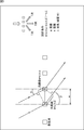
- FIG. 5 shows an example of a diffraction grating.
- a plurality of scatterers constituting the diffraction grating are arranged with a period w, and incident light is incident at an angle ⁇ .
- interference occurs due to a plurality of scattered lights.
- the optical path difference between two adjacent light beams is w ⁇ sin ⁇ on the incident side, and the optical path difference is w on the exit side. ⁇ Sin ⁇ .
- the condition for strengthening by interference is expressed by the following equation (1) in consideration of the minus ⁇ side on the emission side.
- w ⁇ (sin ⁇ ⁇ sin ⁇ ) m ⁇ ⁇ (1)
- n is the refractive index of the medium.
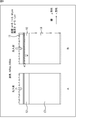
- FIG. 6 shows a configuration example of a solid-state imaging device adopted for wave simulation.
- FIG. 1A shows a conventional configuration example in which the first PD 12 and the second PD 13 are stacked in the Si substrate and the diffraction grating 11 is not provided.
- FIG. 7B is a configuration example to which the present disclosure is applied, in which the first PD 12 and the second PD 13 are stacked in the Si substrate, and the diffraction grating 11 is provided on the second PD 13.
- the first PD 12 absorbs short wavelength light such as the B component
- the second PD 13 absorbs long wavelength light such as the R component.
- the wavelength of incident light is 460 nm (B component) and 640 nm (R component)
- the period w of the diffraction grating 11 is 0.1 to 0.18 ⁇ m (100 to 180 nm)
- the groove depth d is 0.1 ⁇ m. .
- FIG. 7 shows a simulation result when the wavelength of incident light is 460 nm.
- FIG. 6A shows the case where the diffraction grating 11 is not provided
- FIG. 6B shows the case where the diffraction grating 11 is provided.
- the layer thickness of the first PD 12 is 0.6 ⁇ m
- the period w of the diffraction grating 11 is 0.13 ⁇ m.
- FIG. 8 shows a simulation result when the wavelength of incident light is 640 nm.
- FIG. 6A shows the case where the diffraction grating 11 is not provided
- FIG. 6B shows the case where the diffraction grating 11 is provided.
- the layer thickness of the first PD 12 is 0.6 ⁇ m
- the period w of the diffraction grating 11 is 0.13 ⁇ m.
- FIG. 7A and FIG. 8A show that when the diffraction grating 11 is not provided, both the B component and the R component go straight in the vertical direction in the Si substrate.
- the B component is diffracted and travels in the lateral direction in the first PD 12 from the results shown in FIG. 7B and FIG. 8B.
- the R component goes straight in the vertical direction. This is because the diffraction condition is satisfied for the B component and the diffraction condition is not satisfied for the R component.
- the B component since the absorption coefficient is large, the influence of the color mixture on the adjacent pixels is small even if the image proceeds in the horizontal direction.
- a reflecting plate or a film that absorbs light may be provided at the boundary between the pixels to block leakage light.
- FIG. 9 shows the light absorption sensitivity improvement rate of the first PD 12 (curve B) and the second PD 13 (curve R) when the period w of the diffraction grating 11 is changed.
- the sensitivity improvement rate is 1 when the diffraction grating 11 is not provided. In the case shown in the figure, it is assumed that the diffraction grating 11 is provided in the xy direction.
- the sensitivity is significantly improved in the first PD 12 that absorbs the B component.
- FIG. 10 shows a wave simulation result when the wavelength of the incident light is 640 nm and the period w of the diffraction grating 11 is changed from 0.1 to 0.18 ⁇ m. From FIG. A to FIG. w is increased.
- the R component hardly diffracts in the lateral direction when the period w is from 0.1 to 0.16 ⁇ m, and the R component is diffracted in the lateral direction when the cycle w is 0.18 ⁇ m. You can see that Therefore, it can be said that the optimum range of the period w for preventing the R component from being mixed with adjacent pixels is 0.1 to 0.16 ⁇ m.
- the value B is the sensitivity of the first PD 12 to light having a wavelength of 460 nm
- the value ⁇ B is the sensitivity of the first PD 12 to light having a wavelength of 640 nm
- the value R is the sensitivity of the second PD 13 to light having a wavelength of 640 nm
- the value ⁇ R is the sensitivity of the second PD 13 to light having a wavelength of 460 nm.
- the value ⁇ B / B is defined as a color mixing index in the first PD 12
- the value ⁇ R / R is defined as a color mixing index in the second PD 13.
- both the indexes ⁇ B / B and ⁇ R / R are decreased when the diffraction grating 11 is provided, compared to when the diffraction grating 11 is not provided. This means that the color mixture is decreasing.
- the reason why the index ⁇ B / B decreases is considered to be that the value PD, which is the denominator of the index ⁇ B / B, increases as the absorption of light having a wavelength of 460 nm in the first PD 12 increases.
- the reason why the index ⁇ R / R is decreasing is that light having a wavelength of 460 nm reaching the second PD 13 decreases, absorption in the second PD 13 decreases, and the value ⁇ R that is a numerator of the index ⁇ R / R decreases. This is probably because of this.
- the color mixture in the same pixel can be reduced by providing the diffraction grating 11. Thereby, the noise propagation after the signal processing of the color correction calculation can be reduced, and the deterioration of the SN ratio can be suppressed.
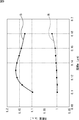
- FIG. 12 shows the sensitivity to the R component (wavelength 640 nm) in the second PD 13 when the layer thickness of the first PD 12 is changed in the range of 0.4 to 0.6 ⁇ m.
- FIG. 13 shows the color mixture index ⁇ B / B of the first PD 12 when the thickness of the layer of the first PD 12 is changed in the range of 0.4 to 0.6 ⁇ m.
- the period w of the diffraction grating 11 in FIGS. 12 and 13 is 0.13 ⁇ m.
- the spectral sensitivity characteristics can be further improved by providing the diffraction grating 11 and further reducing the thickness of the first PD 12 layer.
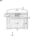
- FIG. 14 illustrates a first configuration example of the solid-state imaging element according to the embodiment of the present disclosure.
- the solid-state imaging device 20 includes an on-chip lens (OCL) 21, an organic photoelectric conversion film 22, a diffraction grating 23, a first PD (B-PD) 24, and a second PD (R-PD) 25 in order from the light incident side.
- OCL on-chip lens
- B-PD organic photoelectric conversion film
- R-PD second PD
- the electrode is provided in each of the organic photoelectric converting film 22, 1st PD24, and 2nd PD25, the detailed description is abbreviate
- the on-chip lens 21 collects incident light near the center of the pixel.
- the organic photoelectric conversion film 22 absorbs the G component light of the incident light and converts it into charges.
- the diffraction grating 23 diffracts the B component of the incident light transmitted through the organic photoelectric conversion film 22 in the lateral direction and causes other components to travel straight.
- the period w of the diffraction grating 23 is in the range of 0.1 to 0.16 ⁇ m, for example, 0.13 ⁇ m (130 nm), and the groove depth d is, for example, 100 nm.
- the first PD 24 absorbs the B component diffracted by the diffraction grating 23 and converts it into electric charges.
- the thickness of the first PD 24 is 0.6 ⁇ m or less, for example, 0.5 ⁇ m.
- the second PD 25 absorbs the R component of the incident light transmitted through the first PD 24 and converts it into electric charges.
- the layer of the second PD 25 is formed with a thickness of 2.5 ⁇ m, for example.
- incident light is collected near the center of the pixel by the on-chip lens 21, and first, the G component light of the incident light is absorbed by the organic photoelectric conversion film 22 and converted into electric charge. Next, the B component of the incident light transmitted through the organic photoelectric conversion film 22 is diffracted in the lateral direction by the diffraction grating 23 and absorbed by the first PD 24 to be converted into electric charges. The R component of the incident light that travels straight without being diffracted by the diffraction grating 23 is absorbed by the second PD 25 and converted into electric charge.
- a reflecting plate or a film that absorbs light may be provided at the boundary between the pixels to block leakage light.
- the diffraction grating 23 in which scatterers are arranged at an appropriate period is provided and the first PD 24 having a thin layer is formed, color mixing for each pixel is unavoidable structurally. Can be suppressed, and a decrease in sensitivity of each color component is suppressed.
- the photosensitivity characteristics of each pixel of the solid-state image sensor 20 approach the ideal spectrum, the matrix coefficient of the color correction calculation in the subsequent stage of the solid-state image sensor 20 is suppressed, and as a result, the deterioration of the SN ratio is suppressed. An image with an image quality can be obtained.
- FIG. 15 illustrates a second configuration example of the solid-state imaging element according to the embodiment of the present disclosure.
- the solid-state imaging device 30 includes a first pixel 30A that simultaneously outputs a pixel signal of a B component and an R component, and a second pixel 30B that outputs a pixel signal of a G component. Is arranged.
- the first pixel 30A includes, in order from the light incident side, an on-chip lens 31, an on-chip color filter (OCCF) 32M colored with magenta, a diffraction grating 33, and a first PD ( B-PD) 34 and second PD (R-PD) 35 are laminated.
- the second pixel 30B is configured by laminating an on-chip lens 31, an on-chip color filter 32G colored with G (Green), and a third PD (G-PD) 36 in order from the light incident side.
- the first PD 34, the second PD 35, and the third PD 36 are each provided with an electrode, but detailed description thereof is omitted.
- the on-chip lens 31 collects incident light near the center of the pixel.
- the on-chip color filter 32 is colored magenta or G in pixel units.
- the diffraction grating 33 diffracts the B component of the incident light transmitted through the on-chip color filter 32M in the lateral direction and causes other components to travel straight.
- the period w of the diffraction grating 33 is in the range of 0.1 to 0.16 ⁇ m, for example, 0.13 ⁇ m (130 nm), and the groove depth d is, for example, 100 nm.
- the first PD 34 absorbs the B component diffracted by the diffraction grating 33 and converts it into electric charges.
- the first PD 34 is formed with a thickness of 0.6 ⁇ m or less, for example, 0.5 ⁇ m.
- the second PD 35 absorbs the R component of the incident light transmitted through the first PD 34 and converts it into electric charges.
- the thickness of the second PD 35 is, for example, 2.5 ⁇ m.
- the third PD 36 absorbs the G component of the incident light transmitted through the on-chip color filter 32G and converts it into electric charges.
- first pixel 30 ⁇ / b> A of the solid-state imaging device 30 incident light is collected near the center of the pixel by the on-chip lens 31, and the B component of the incident light transmitted through the on-chip color filter 32 ⁇ / b> M is laterally transmitted by the diffraction grating 33. It is diffracted and absorbed by the first PD 34 to be converted into electric charge. The R component of the incident light that travels straight without being diffracted by the diffraction grating 33 is absorbed by the second PD 35 and converted into an electric charge.
- a reflecting plate or a film that absorbs light may be provided at the boundary between the pixels to block leakage light.
- the incident light is condensed near the center of the pixel by the on-chip lens 31, and the G component of the incident light transmitted through the on-chip color filter 32G is absorbed by the third PD 36 and converted into electric charge. .
- the first pixel 30A of the solid-state imaging device 30 is provided with a diffraction grating 33 in which scatterers are arranged at an appropriate period, and further, a thinned first PD 34 is formed. It is possible to suppress color mixture for each pixel that is not present, and to suppress a decrease in sensitivity of each color component. Further, since the photosensitivity characteristic of each pixel of the solid-state image sensor 30 approaches the ideal spectrum, the matrix coefficient of the color correction calculation in the subsequent stage of the solid-state image sensor 30 can be suppressed low, and as a result, the deterioration of the SN ratio can be suppressed. An image with an image quality can be obtained.
- FIG. 16 illustrates a third configuration example of the solid-state imaging element according to the embodiment of the present disclosure.
- the solid-state imaging device 40 includes, in order from the light incident side, an on-chip lens 41, a B diffraction grating 42, a first PD (B-PD) 43, a G diffraction grating 44, a second PD (G-PD) 45, and A third PD (R-PD) 46 is laminated.
- the first PD 43, the second PD 45, and the third PD 46 are each provided with an electrode, but detailed description thereof is omitted.
- the on-chip lens 41 condenses incident light near the center of the pixel.
- the B diffraction grating 42 diffracts the B component of the incident light in the lateral direction and causes other components to travel straight.
- the period w of the B diffraction grating 42 is in the range of 0.1 to 0.16 ⁇ m, for example, 0.13 ⁇ m (130 nm), and the groove depth d is, for example, 100 nm.
- the first PD 43 absorbs the B component diffracted by the B diffraction grating 33 and converts it into charges.
- the first PD 43 is formed with a thickness of 0.6 ⁇ m or less, for example, 0.5 ⁇ m.
- the G diffraction grating 44 diffracts the G component of the incident light in the lateral direction and causes other components to travel straight.
- the period w of the G diffraction grating 44 is in the range of 0.1 to 0.16 ⁇ m, for example, 0.15 ⁇ m (150 nm), and the groove depth d is, for example, 100 nm.
- the second PD 45 absorbs the G component diffracted by the G diffraction grating 44 and converts it into charges.
- the thickness of the second PD45 is formed to be 1.8 ⁇ m, for example.
- 3rd PD46 absorbs R component of the incident light which permeate
- the layer thickness of the third PD 46 is, for example, 2.6 ⁇ m.
- incident light is collected near the center of the pixel by the on-chip lens 41, and its B component is diffracted laterally by the B diffraction grating 42 and absorbed by the first PD 34 to be converted into electric charge.
- the incident light that has traveled straight without being diffracted by the diffraction grating 33 is diffracted in the lateral direction by the G diffraction grating 44 and absorbed by the second PD 45 to be converted into electric charges.
- the R component of the incident light transmitted through the first PD 43 and the second PD 45 is absorbed by the third PD 46 and converted into electric charges.
- a reflecting plate or a film that absorbs light may be provided at the boundary between the pixels to block leakage light.
- the B diffraction grating 42 and the G diffraction grating 44 in which scatterers are arranged at an appropriate period are provided, and further, the first PD 43 and the second PD 45 that are thinned are formed.
- the matrix coefficient of the color correction calculation at the subsequent stage of the solid-state image sensor 40 is suppressed, and as a result, the deterioration of the SN ratio is suppressed. An image with an image quality can be obtained.
- FIG. 17 shows a manufacturing process of the solid-state imaging device 40.
- the third PD 46 and the second PD 45 are formed in the Si substrate. Specifically, an n-type (or p-type) impurity is doped into the Si substrate by ion implantation, the impurity is activated by annealing, or an n-type (or p-type) impurity is doped during Si epitaxial growth. Thus, the third PD 46 and the second PD 45 are formed.
- the n-type impurity P, As, Sb, Bi, or the like can be adopted.
- As the p-type impurity B, In or the like can be adopted.
- the G diffraction grating 44 is formed on the outermost surface of the second PD 45. Specifically, after applying a resist film at equal intervals by a lithography technique on a film of an inorganic material (oxide, nitride, etc.) having a lower refractive index than Si, periodic diffraction by G is performed by dry etching. A lattice 44 is formed. Thereafter, the damaged layer on the surface may be further removed by chemical etching and tapered.
- the first PD 43 is formed in the same manner as the second PD 45 and the like.
- the B diffraction grating 42 is formed on the first PD 43. Specifically, a resist film is formed at equal intervals by lithography, and then the unevenness that becomes the B diffraction grating 42 is formed by dry etching. Finally, a through electrode is formed.
- light of a predetermined wavelength of incident light is generated by surface plasmon resonance (SPR) generated by arranging metal nanoparticles or nanowires instead of the diffraction grating. It bends in the horizontal direction.
- SPR surface plasmon resonance
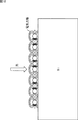
- FIG. 18 shows the principle of surface plasmon resonance.
- surface plasmon resonance occurs when metal nanoparticles (or metal nanowires) are arranged on the Si surface.
- metal nanoparticles In metal nanoparticles, a photoelectric field and plasmon are coupled to cause light absorption, and an electric field that is significantly enhanced locally is generated. At this time, the light energy is converted into surface plasmons, which propagate through the metal surface or between the metal surfaces, allowing the light to travel in the lateral direction. Furthermore, this electric field can be absorbed from the Si surface as near-field light.
- silver can be used as the metal material that resonates with the light of the B component
- gold can be used as the material that resonates with the light of the G component.
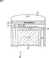
- FIG. 19 illustrates a fourth configuration example of the solid-state imaging element according to the embodiment of the present disclosure.
- This solid-state image pickup device 50 is a modification of the solid-state image pickup device 20 shown in FIG. 14, in which the diffraction grating 23 in the solid-state image pickup device 20 is replaced with silver nanoparticles (which may be silver nanowires) 51 having a diameter of 100 nm or less. It is.
- the other components are denoted by the same reference numerals as those of the solid-state imaging device 20, and the description thereof is omitted.
- silver nanoparticles 51 for example, silver nanoparticles are colloidally dispersed in an organic liquid in advance and applied to the outermost surface of the first PD 24 by spin coating, or silver nanoparticles are formed by vacuum deposition. Can be attached.
- the arrangement of the silver nanoparticles 51 is not necessarily the Si surface but may be in the vicinity of the Si surface in order to reduce dark current.
- the near-field light may be disposed in a range where it reaches Si, for example, at a distance of 300 nm or less from the Si surface.
- solid-state imaging device 50 surface plasmons are generated by the silver nanoparticles 51 according to the light of the B component, the B component propagates in the lateral direction, and other components travel straight. Therefore, the same operations and effects as those of the solid-state image sensor 20 can be obtained.
- FIG. 20 illustrates a fifth configuration example of the solid-state imaging element according to the embodiment of the present disclosure.
- This solid-state imaging device 60 is a modification of the solid-state imaging device 30 shown in FIG. 15, and silver nanoparticles (or silver nanowires) having a diameter of 100 nm or less as the diffraction grating 33 in the first pixel 30A of the solid-state imaging device 30 are used. 61 is substituted.
- Other components are denoted by the same reference numerals as those of the solid-state imaging device 30, and the description thereof is omitted.
- the formation of the silver nanoparticles 61 is the same as the formation of the silver nanoparticles 51 in the solid-state imaging device 50, the description thereof is omitted.
- solid-state imaging device 60 surface plasmons are generated by the silver nanoparticles 61 according to the light of the B component, the B component propagates in the lateral direction, and the other components travel straight. Therefore, the same operation and effect as the solid-state imaging device 50 can be obtained.
- FIG. 21 is a diagram illustrating a usage example in which the above-described solid-state imaging device is used.
- the solid-state imaging device described above can be used in various cases for sensing light such as visible light, infrared light, ultraviolet light, and X-ray as follows.
- Devices for taking images for viewing such as digital cameras and mobile devices with camera functions
- Devices used for traffic such as in-vehicle sensors that capture the back, surroundings, and interiors of vehicles, surveillance cameras that monitor traveling vehicles and roads, and ranging sensors that measure distances between vehicles, etc.
- Equipment used for home appliances such as TVs, refrigerators, air conditioners, etc. to take pictures and operate the equipment according to the gestures ⁇ Endoscopes, equipment that performs blood vessel photography by receiving infrared light, etc.
- Equipment used for medical and health care ⁇ Security equipment such as security surveillance cameras and personal authentication cameras ⁇ Skin measuring instrument for photographing skin and scalp photography Such as a microscope to do beauty Equipment used for sports-Equipment used for sports such as action cameras and wearable cameras for sports applications-Used for agriculture such as cameras for monitoring the condition of fields and crops apparatus
- a solid-state imaging device including a vertical spectral structure pixel in which a plurality of photoelectric conversion units are stacked,
- the vertical spectral structure pixel is A first photoelectric conversion unit that generates a charge in response to light of a first wavelength of incident light;
- a second photoelectric conversion unit that generates a charge in response to light having a second wavelength among the incident light transmitted through the first photoelectric conversion unit;
- a solid-state imaging device comprising: a first spectroscopic unit that is formed on an upper surface of the first photoelectric conversion unit and bends the traveling direction of the light having the first wavelength of the incident light in a lateral direction.
- the vertical spectral structure pixel is A third photoelectric converter that generates a charge in response to light of the third wavelength of incident light;
- the first photoelectric conversion unit transmits the third photoelectric conversion unit, and generates a charge according to the light of the first wavelength whose traveling direction is bent by the first spectroscopic unit,
- the second photoelectric conversion unit is configured to respond to light having the second wavelength among the incident light transmitted through the third photoelectric conversion unit, the first spectroscopic unit, and the first photoelectric conversion unit.
- the solid-state imaging device according to any one of (1) to (6).
- the first and second photoelectric conversion units are PDs
- the first to third photoelectric conversion units are PDs.
- the non-longitudinal spectral structure pixel is A color filter that transmits only the light of the third wavelength on the upper surface of the third photoelectric conversion unit;
- the vertical spectral structure pixel is The solid-state imaging device according to (9) or (10), further including a color filter that transmits only light of the first and second wavelengths on an upper surface of the first spectroscopic unit.
- the vertical spectral structure pixel is A third photoelectric conversion unit that generates a charge in response to light of a third wavelength of incident light; A second spectroscopic unit formed on an upper surface of the third photoelectric conversion unit and configured to bend a traveling direction of the light having the third wavelength of the incident light in a lateral direction; The third photoelectric conversion unit generates an electric charge according to light of the third wavelength among the incident light transmitted through the first spectroscopic unit and the first photoelectric conversion unit, The second photoelectric conversion unit includes the first light splitting unit, the first photoelectric conversion unit, the second light splitting unit, and the third photoelectric conversion unit of the incident light transmitted through the third photoelectric conversion unit.
- the solid-state imaging device according to any one of (1) to (6), wherein charge is generated in response to light having a wavelength of 2.
- the solid-state imaging device wherein the second spectroscopic unit is a diffraction grating, a metal nanoparticle, or a metal nanowire.
- or 3rd photoelectric conversion part is PD.
- the solid-state image sensor as described in said (12).
- the vertical spectral structure pixel is The solid-state imaging device according to any one of (1) to (14), further including a condensing unit that condenses the incident light near a center of the vertical spectral structure pixel.
- the light of the first wavelength is B component light
- the light of the second wavelength is R component light
- the solid-state imaging device according to any one of (7) to (15), wherein the light having the third wavelength is G-component light.
- (17) In an electronic device equipped with a solid-state imaging device including a vertical spectral structure pixel in which a plurality of photoelectric conversion units are stacked, The vertical spectral structure pixel is A first photoelectric conversion unit that generates a charge in response to light of a first wavelength of incident light; A second photoelectric conversion unit that generates a charge in response to light having a second wavelength among the incident light transmitted through the first photoelectric conversion unit;
- An electronic device comprising: a first spectroscopic unit formed on an upper surface of the first photoelectric conversion unit and configured to bend a traveling direction of the light having the first wavelength of the incident light in a lateral direction.
Landscapes
- Chemical & Material Sciences (AREA)
- Engineering & Computer Science (AREA)
- Nanotechnology (AREA)
- Health & Medical Sciences (AREA)
- Life Sciences & Earth Sciences (AREA)
- General Health & Medical Sciences (AREA)
- Molecular Biology (AREA)
- Crystallography & Structural Chemistry (AREA)
- Solid State Image Pick-Up Elements (AREA)
- Transforming Light Signals Into Electric Signals (AREA)
- Color Television Image Signal Generators (AREA)
Abstract
Description
図3は、本開示を適用した縦方向分光構造を有する固体撮像素子の概略断面図である。
次に、回折格子による作用について説明する。
w・(sinα±sinβ)=m・λ ・・・(1)
w≒λ0/n ・・・(2)
次に、第1PD12の層の厚さを薄くすることの効果について説明する。
次に、図14は、本開示の実施の形態である固体撮像素子の第1の構成例を示している。
次に、図15は、本開示の実施の形態である固体撮像素子の第2の構成例を示している。
次に、図16は、本開示の実施の形態である固体撮像素子の第3の構成例を示している。
上述した固体撮像素子の第1乃至第3の構成例では、入射光のうちの所定の波長の光を回折格子によって回折させるようにした。
図19は、本開示の実施の形態である固体撮像素子の第4の構成例を示している。この固体撮像素子50は、図14に示された固体撮像素子20の変形例であり、固体撮像素子20における回折格子23を直径100nm以下の銀ナノ粒子(銀ナノワイヤでもよい)51に置換したものである。その他の構成要素については、固体撮像素子20の構成要素と同一の符号を付しているので、その説明は省略する。
図20は、本開示の実施の形態である固体撮像素子の第5の構成例を示している。この固体撮像素子60は、図15に示された固体撮像素子30の変形例であり、固体撮像素子30の第1画素30Aにおける回折格子33を直径100nm以下の銀ナノ粒子(銀ナノワイヤでもよい)61に置換したものである。その他の構成要素については、固体撮像素子30の構成要素と同一の符号を付しているので、その説明は省略する。
図21は、上述の固体撮像素子を使用する使用例を示す図である。
・自動停止等の安全運転や、運転者の状態の認識等のために、自動車の前方や後方、周囲、車内等を撮影する車載用センサ、走行車両や道路を監視する監視カメラ、車両間等の測距を行う測距センサ等の、交通の用に供される装置
・ユーザのジェスチャを撮影して、そのジェスチャに従った機器操作を行うために、TVや、冷蔵庫、エアーコンディショナ等の家電に供される装置
・内視鏡や、赤外光の受光による血管撮影を行う装置等の、医療やヘルスケアの用に供される装置
・防犯用途の監視カメラや、人物認証用途のカメラ等の、セキュリティの用に供される装置
・肌を撮影する肌測定器や、頭皮を撮影するマイクロスコープ等の、美容の用に供される装置
・スポーツ用途等向けのアクションカメラやウェアラブルカメラ等の、スポーツの用に供される装置
・畑や作物の状態を監視するためのカメラ等の、農業の用に供される装置
(1)
複数の光電変換部が積層された縦方向分光構造画素を含む固体撮像素子において、
前記縦方向分光構造画素は、
入射光のうちの第1の波長の光に応じて電荷を発生する第1の光電変換部と、
前記第1の光電変換部を透過した前記入射光のうちの第2の波長の光に応じて電荷を発生する第2の光電変換部と、
前記第1の光電変換部の上面に形成された、前記入射光の前記第1の波長の光の進行方向を横方向に曲げる第1の分光部とを備える
固体撮像素子。
(2)
前記第1の分光部は、前記入射光の前記第1の波長の光の進行方向を、前記第1の光電変換部の延伸方向に曲げる
前記(1)に記載の固体撮像素子。
(3)
前記第1の分光部は、前記入射光の前記第1の波長以外の光の進行方向を変えずに直進させる
前記(1)または(2)に記載の固体撮像素子。
(4)
前記第1の分光部は、回折格子である
前記(1)から(3)のいずれかに記載の固体撮像素子。
(5)
前記第1の分光部は、金属ナノ粒子または金属ナノワイヤである
前記(1)から(3)のいずれかに記載の固体撮像素子。
(6)
前記第1の光電変換部の層の厚さは、前記第2の光電変換部の操作の厚さに比較して薄く形成されている
前記(1)から(5)のいずれかに記載の固体撮像素子。
(7)
前記縦方向分光構造画素は、
入射光のうちの第3の波長の光に応じて電荷を発生する第3の光電変換部をさらに備え、
前記第1の光電変換部は、前記第3の光電変換部を透過し、前記第1の分光部によって進行方向が曲げられた前記第1の波長の光に応じて電荷を発生し、
前記第2の光電変換部は、前記第3の光電変換部、前記第1の分光部、および前記第1の光電変換部を透過した前記入射光のうちの前記第2の波長の光に応じて電荷を発生する
前記(1)から(6)のいずれかに記載の固体撮像素子。
(8)
前記第1および第2の光電変換部は、PDであり、
前記第3の光電変換部は、有機光電変換膜である
前記(1)から(7)のいずれかに記載の固体撮像素子。
(9)
入射光のうちの第3の波長の光に応じて電荷を発生する第3の光電変換部を備える非縦方向分光構造画素をさらに含む
前記(1)から(6)のいずれかに記載の固体撮像素子。
(10)
前記第1乃至第3の光電変換部は、PDである
前記(9)に記載の固体撮像素子。
(11)
前記非縦方向分光構造画素は、
前記第3の光電変換部の上面に前記第3の波長の光のみを透過するカラーフィルタをさらに備え、
前記縦方向分光構造画素は、
前記第1の分光部の上面に前記第1および第2の波長の光のみを透過するカラーフィルタをさらに備える
前記(9)または(10)に記載の固体撮像素子。
(12)
前記縦方向分光構造画素は、
入射光のうちの第3の波長の光に応じて電荷を発生する第3の光電変換部と、
前記第3の光電変換部の上面に形成された、前記入射光の前記第3の波長の光の進行方向を横方向に曲げる第2の分光部とをさらに備え、
前記第3の光電変換部は、前記第1の分光部、および前記第1の光電変換部を透過した前記入射光のうちの前記第3の波長の光に応じて電荷を発生し、
前記第2の光電変換部は、前記第1の分光部、前記第1の光電変換部、前記第2の分光部、および前記第3の光電変換部を透過した前記入射光のうちの前記第2の波長の光に応じて電荷を発生する
前記(1)から(6)のいずれかに記載の固体撮像素子。
(13)
前記第2の分光部は、回折格子、金属ナノ粒子、または金属ナノワイヤである
前記(12)に記載の固体撮像素子。
(14)
前記第1乃至第3の光電変換部は、PDである
前記(12)に記載の固体撮像素子。
(15)
前記縦方向分光構造画素は、
前記入射光を前記縦方向分光構造画素の中央付近に集光させる集光部をさらに備える
前記(1)から(14)のいずれかに記載の固体撮像素子。
(16)
前記第1の波長の光は、B成分の光であり、
前記第2の波長の光は、R成分の光であり、
前記第3の波長の光は、G成分の光である
前記(7)から(15)のいずれかに記載の固体撮像素子。
(17)
複数の光電変換部が積層された縦方向分光構造画素を含む固体撮像素子が搭載された電子装置において、
前記縦方向分光構造画素は、
入射光のうちの第1の波長の光に応じて電荷を発生する第1の光電変換部と、
前記第1の光電変換部を透過した前記入射光のうちの第2の波長の光に応じて電荷を発生する第2の光電変換部と、
前記第1の光電変換部の上面に形成された、前記入射光の前記第1の波長の光の進行方向を横方向に曲げる第1の分光部とを備える
電子装置。
Claims (17)
- 複数の光電変換部が積層された縦方向分光構造画素を含む固体撮像素子において、
前記縦方向分光構造画素は、
入射光のうちの第1の波長の光に応じて電荷を発生する第1の光電変換部と、
前記第1の光電変換部を透過した前記入射光のうちの第2の波長の光に応じて電荷を発生する第2の光電変換部と、
前記第1の光電変換部の上面に形成された、前記入射光の前記第1の波長の光の進行方向を横方向に曲げる第1の分光部とを備える
固体撮像素子。 - 前記第1の分光部は、前記入射光の前記第1の波長の光の進行方向を、前記第1の光電変換部の延伸方向に曲げる
請求項1に記載の固体撮像素子。 - 前記第1の分光部は、前記入射光の前記第1の波長以外の光の進行方向を変えずに直進させる
請求項2に記載の固体撮像素子。 - 前記第1の分光部は、回折格子である
請求項2に記載の固体撮像素子。 - 前記第1の分光部は、金属ナノ粒子または金属ナノワイヤである
請求項2に記載の固体撮像素子。 - 前記第1の光電変換部の層の厚さは、前記第2の光電変換部の操作の厚さに比較して薄く形成されている
請求項2に記載の固体撮像素子。 - 前記縦方向分光構造画素は、
入射光のうちの第3の波長の光に応じて電荷を発生する第3の光電変換部をさらに備え、
前記第1の光電変換部は、前記第3の光電変換部を透過し、前記第1の分光部によって進行方向が曲げられた前記第1の波長の光に応じて電荷を発生し、
前記第2の光電変換部は、前記第3の光電変換部、前記第1の分光部、および前記第1の光電変換部を透過した前記入射光のうちの前記第2の波長の光に応じて電荷を発生する
請求項2に記載の固体撮像素子。 - 前記第1および第2の光電変換部は、PDであり、
前記第3の光電変換部は、有機光電変換膜である
請求項7に記載の固体撮像素子。 - 入射光のうちの第3の波長の光に応じて電荷を発生する第3の光電変換部を備える非縦方向分光構造画素をさらに含む
請求項2に記載の固体撮像素子。 - 前記第1乃至第3の光電変換部は、PDである
請求項9に記載の固体撮像素子。 - 前記非縦方向分光構造画素は、
前記第3の光電変換部の上面に前記第3の波長の光のみを透過するカラーフィルタをさらに備え、
前記縦方向分光構造画素は、
前記第1の分光部の上面に前記第1および第2の波長の光のみを透過するカラーフィルタをさらに備える
請求項9に記載の固体撮像素子。 - 前記縦方向分光構造画素は、
入射光のうちの第3の波長の光に応じて電荷を発生する第3の光電変換部と、
前記第3の光電変換部の上面に形成された、前記入射光の前記第3の波長の光の進行方向を横方向に曲げる第2の分光部とをさらに備え、
前記第3の光電変換部は、前記第1の分光部、および前記第1の光電変換部を透過した前記入射光のうちの前記第3の波長の光に応じて電荷を発生し、
前記第2の光電変換部は、前記第1の分光部、前記第1の光電変換部、前記第2の分光部、および前記第3の光電変換部を透過した前記入射光のうちの前記第2の波長の光に応じて電荷を発生する
請求項2に記載の固体撮像素子。 - 前記第2の分光部は、回折格子、金属ナノ粒子、または金属ナノワイヤである
請求項12に記載の固体撮像素子。 - 前記第1乃至第3の光電変換部は、PDである
請求項12に記載の固体撮像素子。 - 前記縦方向分光構造画素は、
前記入射光を前記縦方向分光構造画素の中央付近に集光させる集光部をさらに備える
請求項2に記載の固体撮像素子。 - 前記第1の波長の光は、B成分の光であり、
前記第2の波長の光は、R成分の光であり、
前記第3の波長の光は、G成分の光である
請求項7に記載の固体撮像素子。 - 複数の光電変換部が積層された縦方向分光構造画素を含む固体撮像素子が搭載された電子装置において、
前記縦方向分光構造画素は、
入射光のうちの第1の波長の光に応じて電荷を発生する第1の光電変換部と、
前記第1の光電変換部を透過した前記入射光のうちの第2の波長の光に応じて電荷を発生する第2の光電変換部と、
前記第1の光電変換部の上面に形成された、前記入射光の前記第1の波長の光の進行方向を横方向に曲げる第1の分光部とを備える
電子装置。
Priority Applications (3)
| Application Number | Priority Date | Filing Date | Title |
|---|---|---|---|
| JP2017502072A JPWO2016136502A1 (ja) | 2015-02-26 | 2016-02-12 | 固体撮像素子、および電子装置 |
| US15/549,231 US10403662B2 (en) | 2015-02-26 | 2016-02-12 | Solid-state imaging element and electronic apparatus |
| CN201680011090.1A CN107251224B (zh) | 2015-02-26 | 2016-02-12 | 固态成像元件和电子设备 |
Applications Claiming Priority (2)
| Application Number | Priority Date | Filing Date | Title |
|---|---|---|---|
| JP2015-036248 | 2015-02-26 | ||
| JP2015036248 | 2015-02-26 |
Publications (1)
| Publication Number | Publication Date |
|---|---|
| WO2016136502A1 true WO2016136502A1 (ja) | 2016-09-01 |
Family
ID=56789572
Family Applications (1)
| Application Number | Title | Priority Date | Filing Date |
|---|---|---|---|
| PCT/JP2016/054145 Ceased WO2016136502A1 (ja) | 2015-02-26 | 2016-02-12 | 固体撮像素子、および電子装置 |
Country Status (4)
| Country | Link |
|---|---|
| US (1) | US10403662B2 (ja) |
| JP (1) | JPWO2016136502A1 (ja) |
| CN (1) | CN107251224B (ja) |
| WO (1) | WO2016136502A1 (ja) |
Cited By (4)
| Publication number | Priority date | Publication date | Assignee | Title |
|---|---|---|---|---|
| JPWO2021015070A1 (ja) * | 2019-07-22 | 2021-01-28 | ||
| WO2021140958A1 (ja) * | 2020-01-10 | 2021-07-15 | ソニーセミコンダクタソリューションズ株式会社 | 撮像素子、製造方法、並びに電子機器 |
| JP2024526783A (ja) * | 2021-07-16 | 2024-07-19 | ホアウェイ・テクノロジーズ・カンパニー・リミテッド | 画像センサ及び電子デバイス |
| JP2024153671A (ja) * | 2019-06-21 | 2024-10-29 | ソニーセミコンダクタソリューションズ株式会社 | 光電変換素子、光検出装置、光検出システム、電子機器および移動体 |
Families Citing this family (9)
| Publication number | Priority date | Publication date | Assignee | Title |
|---|---|---|---|---|
| CN107438148B (zh) * | 2016-05-27 | 2021-08-24 | 松下知识产权经营株式会社 | 摄像系统 |
| JP6920110B2 (ja) * | 2017-06-13 | 2021-08-18 | ルネサスエレクトロニクス株式会社 | 固体撮像素子およびその製造方法 |
| EP3671837B1 (en) | 2018-12-21 | 2023-11-29 | ams Sensors Belgium BVBA | Pixel of a semiconductor image sensor and method of manufacturing a pixel |
| CN110611778B (zh) * | 2019-09-06 | 2022-04-12 | Oppo广东移动通信有限公司 | 图像传感器、图像处理方法和装置、及存储介质 |
| CN110677605B (zh) * | 2019-09-12 | 2022-04-12 | Oppo广东移动通信有限公司 | 一种叠层cis、图像处理方法及存储介质和终端设备 |
| CN110691207A (zh) * | 2019-09-18 | 2020-01-14 | Oppo广东移动通信有限公司 | 一种图像传感器及图像处理方法、存储介质 |
| CN110691208B (zh) * | 2019-09-24 | 2022-05-27 | Oppo广东移动通信有限公司 | 图像传感器、图像处理方法和装置、及存储介质 |
| CN110650301B (zh) * | 2019-10-14 | 2022-03-01 | Oppo广东移动通信有限公司 | 图像传感器及成像方法、设备 |
| US12402422B2 (en) * | 2023-06-20 | 2025-08-26 | Taiwan Semiconductor Manufacturing Company, Ltd. | Near infrared light sensor with improved light coupling and CMOS image sensor including same |
Citations (4)
| Publication number | Priority date | Publication date | Assignee | Title |
|---|---|---|---|---|
| JP2011138950A (ja) * | 2009-12-28 | 2011-07-14 | Sony Corp | 半導体装置及び電子機器 |
| JP2011180426A (ja) * | 2010-03-02 | 2011-09-15 | Canon Inc | 分光装置 |
| JP2013093553A (ja) * | 2011-10-04 | 2013-05-16 | Canon Inc | 光電変換装置及びその製造方法、並びに光電変換システム |
| JP2014078673A (ja) * | 2012-09-20 | 2014-05-01 | Sony Corp | 固体撮像装置および固体撮像装置の製造方法ならびに電子機器 |
Family Cites Families (11)
| Publication number | Priority date | Publication date | Assignee | Title |
|---|---|---|---|---|
| US7742208B2 (en) * | 2006-08-21 | 2010-06-22 | Brother International Corporation | Holographic display and methods of manufacture and use |
| FR2914754B1 (fr) * | 2007-04-05 | 2009-07-17 | Commissariat Energie Atomique | Dispositif de concentration de lumiere plan a epaisseur reduite |
| US7639355B2 (en) * | 2007-06-26 | 2009-12-29 | Hewlett-Packard Development Company, L.P. | Electric-field-enhancement structure and detection apparatus using same |
| KR101385250B1 (ko) * | 2007-12-11 | 2014-04-16 | 삼성전자주식회사 | Cmos 이미지 센서 |
| JP5320989B2 (ja) * | 2008-11-07 | 2013-10-23 | ソニー株式会社 | 固体撮像装置、及び電子機器 |
| JP2013084785A (ja) * | 2011-10-11 | 2013-05-09 | Sony Corp | 固体撮像装置、撮像装置 |
| JP2013115417A (ja) * | 2011-11-24 | 2013-06-10 | Ren Solation Co Ltd | 光電変換素子及びその製造方法 |
| CN104205333B (zh) * | 2012-04-02 | 2017-04-12 | 索尼半导体解决方案公司 | 图像拾取单元和电子设备 |
| CN103681728B (zh) | 2012-09-20 | 2018-04-24 | 索尼公司 | 固体摄像装置及其方法以及电子设备 |
| JP2014127519A (ja) * | 2012-12-25 | 2014-07-07 | Sony Corp | 固体撮像素子、及び、電子機器 |
| JP6130221B2 (ja) * | 2013-05-24 | 2017-05-17 | ソニー株式会社 | 固体撮像装置、および電子機器 |
-
2016
- 2016-02-12 JP JP2017502072A patent/JPWO2016136502A1/ja active Pending
- 2016-02-12 CN CN201680011090.1A patent/CN107251224B/zh not_active Expired - Fee Related
- 2016-02-12 US US15/549,231 patent/US10403662B2/en active Active
- 2016-02-12 WO PCT/JP2016/054145 patent/WO2016136502A1/ja not_active Ceased
Patent Citations (4)
| Publication number | Priority date | Publication date | Assignee | Title |
|---|---|---|---|---|
| JP2011138950A (ja) * | 2009-12-28 | 2011-07-14 | Sony Corp | 半導体装置及び電子機器 |
| JP2011180426A (ja) * | 2010-03-02 | 2011-09-15 | Canon Inc | 分光装置 |
| JP2013093553A (ja) * | 2011-10-04 | 2013-05-16 | Canon Inc | 光電変換装置及びその製造方法、並びに光電変換システム |
| JP2014078673A (ja) * | 2012-09-20 | 2014-05-01 | Sony Corp | 固体撮像装置および固体撮像装置の製造方法ならびに電子機器 |
Cited By (6)
| Publication number | Priority date | Publication date | Assignee | Title |
|---|---|---|---|---|
| JP2024153671A (ja) * | 2019-06-21 | 2024-10-29 | ソニーセミコンダクタソリューションズ株式会社 | 光電変換素子、光検出装置、光検出システム、電子機器および移動体 |
| JPWO2021015070A1 (ja) * | 2019-07-22 | 2021-01-28 | ||
| WO2021015070A1 (ja) * | 2019-07-22 | 2021-01-28 | 国立大学法人静岡大学 | 画素、固体撮像装置及び画素の製造方法 |
| JP7493250B2 (ja) | 2019-07-22 | 2024-05-31 | 国立大学法人静岡大学 | 画素、固体撮像装置及び画素の製造方法 |
| WO2021140958A1 (ja) * | 2020-01-10 | 2021-07-15 | ソニーセミコンダクタソリューションズ株式会社 | 撮像素子、製造方法、並びに電子機器 |
| JP2024526783A (ja) * | 2021-07-16 | 2024-07-19 | ホアウェイ・テクノロジーズ・カンパニー・リミテッド | 画像センサ及び電子デバイス |
Also Published As
| Publication number | Publication date |
|---|---|
| US20180040653A1 (en) | 2018-02-08 |
| CN107251224B (zh) | 2022-06-14 |
| CN107251224A (zh) | 2017-10-13 |
| US10403662B2 (en) | 2019-09-03 |
| JPWO2016136502A1 (ja) | 2017-12-07 |
Similar Documents
| Publication | Publication Date | Title |
|---|---|---|
| JPWO2016136502A1 (ja) | 固体撮像素子、および電子装置 | |
| US20220146726A1 (en) | Solid-state imaging device and electronic apparatus | |
| JP7023109B2 (ja) | 固体撮像装置 | |
| TWI416715B (zh) | A solid-state imaging device, a manufacturing method of a solid-state imaging device, and an electronic device | |
| US20120292521A1 (en) | Two-dimensional solid-state imaging device | |
| JP7574860B2 (ja) | 撮像素子及び撮像装置 | |
| US10490586B2 (en) | Solid-state imaging device with light shielding films, method of manufacturing the same, and electronic apparatus | |
| US12408458B2 (en) | Photoelectric conversion element and light receiving device | |
| WO2016129406A1 (ja) | 撮像素子、および電子装置 | |
| CN102257410A (zh) | 光学元件、包含光学元件的图像传感器和包含图像传感器的图像拾取装置 | |
| EP4242702B1 (en) | Optical element, imaging element, and imaging device | |
| WO2017038542A1 (ja) | 固体撮像素子、および電子装置 | |
| CN111989783A (zh) | 摄像装置及摄像系统 | |
| WO2010007792A1 (ja) | 固体撮像素子 | |
| KR100905230B1 (ko) | 이미지 센서 | |
| WO2020085115A1 (ja) | センサ素子および製造方法、並びに電子機器 | |
| WO2020122038A1 (ja) | 固体撮像素子、固体撮像素子の製造方法、及び電子機器 | |
| WO2019097936A1 (ja) | 固体撮像素子及び電子装置 | |
| US20120256285A1 (en) | Solid-state imaging device and electronic apparatus | |
| US20240170514A1 (en) | Solid-state imaging element and electronic apparatus | |
| EP4212920B1 (en) | Optical element, imaging element, and imaging device | |
| WO2023132133A1 (ja) | 光検出装置及び電子機器 | |
| WO2017119317A1 (ja) | 固体撮像素子および製造方法、並びに電子機器 | |
| WO2023021632A1 (ja) | 光学素子、撮像素子及び撮像装置 |
Legal Events
| Date | Code | Title | Description |
|---|---|---|---|
| 121 | Ep: the epo has been informed by wipo that ep was designated in this application |
Ref document number: 16755249 Country of ref document: EP Kind code of ref document: A1 |
|
| ENP | Entry into the national phase |
Ref document number: 2017502072 Country of ref document: JP Kind code of ref document: A |
|
| WWE | Wipo information: entry into national phase |
Ref document number: 15549231 Country of ref document: US |
|
| NENP | Non-entry into the national phase |
Ref country code: DE |
|
| 122 | Ep: pct application non-entry in european phase |
Ref document number: 16755249 Country of ref document: EP Kind code of ref document: A1 |