WO2016136115A1 - 電力変換装置 - Google Patents
電力変換装置 Download PDFInfo
- Publication number
- WO2016136115A1 WO2016136115A1 PCT/JP2015/086234 JP2015086234W WO2016136115A1 WO 2016136115 A1 WO2016136115 A1 WO 2016136115A1 JP 2015086234 W JP2015086234 W JP 2015086234W WO 2016136115 A1 WO2016136115 A1 WO 2016136115A1
- Authority
- WO
- WIPO (PCT)
- Prior art keywords
- partition
- partition wall
- base plate
- circuit unit
- housing
- Prior art date
- Legal status (The legal status is an assumption and is not a legal conclusion. Google has not performed a legal analysis and makes no representation as to the accuracy of the status listed.)
- Ceased
Links
Images





Classifications
-
- H—ELECTRICITY
- H02—GENERATION; CONVERSION OR DISTRIBUTION OF ELECTRIC POWER
- H02M—APPARATUS FOR CONVERSION BETWEEN AC AND AC, BETWEEN AC AND DC, OR BETWEEN DC AND DC, AND FOR USE WITH MAINS OR SIMILAR POWER SUPPLY SYSTEMS; CONVERSION OF DC OR AC INPUT POWER INTO SURGE OUTPUT POWER; CONTROL OR REGULATION THEREOF
- H02M1/00—Details of apparatus for conversion
- H02M1/44—Circuits or arrangements for compensating for electromagnetic interference in converters or inverters
-
- H—ELECTRICITY
- H02—GENERATION; CONVERSION OR DISTRIBUTION OF ELECTRIC POWER
- H02M—APPARATUS FOR CONVERSION BETWEEN AC AND AC, BETWEEN AC AND DC, OR BETWEEN DC AND DC, AND FOR USE WITH MAINS OR SIMILAR POWER SUPPLY SYSTEMS; CONVERSION OF DC OR AC INPUT POWER INTO SURGE OUTPUT POWER; CONTROL OR REGULATION THEREOF
- H02M3/00—Conversion of DC power input into DC power output
- H02M3/22—Conversion of DC power input into DC power output with intermediate conversion into AC
- H02M3/24—Conversion of DC power input into DC power output with intermediate conversion into AC by static converters
- H02M3/28—Conversion of DC power input into DC power output with intermediate conversion into AC by static converters using discharge tubes with control electrode or semiconductor devices with control electrode to produce the intermediate AC
- H02M3/325—Conversion of DC power input into DC power output with intermediate conversion into AC by static converters using discharge tubes with control electrode or semiconductor devices with control electrode to produce the intermediate AC using devices of a triode or a transistor type requiring continuous application of a control signal
- H02M3/335—Conversion of DC power input into DC power output with intermediate conversion into AC by static converters using discharge tubes with control electrode or semiconductor devices with control electrode to produce the intermediate AC using devices of a triode or a transistor type requiring continuous application of a control signal using semiconductor devices only
- H02M3/33569—Conversion of DC power input into DC power output with intermediate conversion into AC by static converters using discharge tubes with control electrode or semiconductor devices with control electrode to produce the intermediate AC using devices of a triode or a transistor type requiring continuous application of a control signal using semiconductor devices only having several active switching elements
- H02M3/33573—Full-bridge at primary side of an isolation transformer
-
- H—ELECTRICITY
- H02—GENERATION; CONVERSION OR DISTRIBUTION OF ELECTRIC POWER
- H02M—APPARATUS FOR CONVERSION BETWEEN AC AND AC, BETWEEN AC AND DC, OR BETWEEN DC AND DC, AND FOR USE WITH MAINS OR SIMILAR POWER SUPPLY SYSTEMS; CONVERSION OF DC OR AC INPUT POWER INTO SURGE OUTPUT POWER; CONTROL OR REGULATION THEREOF
- H02M3/00—Conversion of DC power input into DC power output
- H02M3/22—Conversion of DC power input into DC power output with intermediate conversion into AC
- H02M3/24—Conversion of DC power input into DC power output with intermediate conversion into AC by static converters
- H02M3/28—Conversion of DC power input into DC power output with intermediate conversion into AC by static converters using discharge tubes with control electrode or semiconductor devices with control electrode to produce the intermediate AC
- H02M3/325—Conversion of DC power input into DC power output with intermediate conversion into AC by static converters using discharge tubes with control electrode or semiconductor devices with control electrode to produce the intermediate AC using devices of a triode or a transistor type requiring continuous application of a control signal
- H02M3/335—Conversion of DC power input into DC power output with intermediate conversion into AC by static converters using discharge tubes with control electrode or semiconductor devices with control electrode to produce the intermediate AC using devices of a triode or a transistor type requiring continuous application of a control signal using semiconductor devices only
- H02M3/33569—Conversion of DC power input into DC power output with intermediate conversion into AC by static converters using discharge tubes with control electrode or semiconductor devices with control electrode to produce the intermediate AC using devices of a triode or a transistor type requiring continuous application of a control signal using semiconductor devices only having several active switching elements
- H02M3/33576—Conversion of DC power input into DC power output with intermediate conversion into AC by static converters using discharge tubes with control electrode or semiconductor devices with control electrode to produce the intermediate AC using devices of a triode or a transistor type requiring continuous application of a control signal using semiconductor devices only having several active switching elements having at least one active switching element at the secondary side of an isolation transformer
- H02M3/33592—Conversion of DC power input into DC power output with intermediate conversion into AC by static converters using discharge tubes with control electrode or semiconductor devices with control electrode to produce the intermediate AC using devices of a triode or a transistor type requiring continuous application of a control signal using semiconductor devices only having several active switching elements having at least one active switching element at the secondary side of an isolation transformer having a synchronous rectifier circuit or a synchronous freewheeling circuit at the secondary side of an isolation transformer
-
- H—ELECTRICITY
- H05—ELECTRIC TECHNIQUES NOT OTHERWISE PROVIDED FOR
- H05K—PRINTED CIRCUITS; CASINGS OR CONSTRUCTIONAL DETAILS OF ELECTRIC APPARATUS; MANUFACTURE OF ASSEMBLAGES OF ELECTRICAL COMPONENTS
- H05K5/00—Casings, cabinets or drawers for electric apparatus
- H05K5/02—Details
- H05K5/0217—Mechanical details of casings
-
- H—ELECTRICITY
- H05—ELECTRIC TECHNIQUES NOT OTHERWISE PROVIDED FOR
- H05K—PRINTED CIRCUITS; CASINGS OR CONSTRUCTIONAL DETAILS OF ELECTRIC APPARATUS; MANUFACTURE OF ASSEMBLAGES OF ELECTRICAL COMPONENTS
- H05K5/00—Casings, cabinets or drawers for electric apparatus
- H05K5/04—Metal casings
-
- H—ELECTRICITY
- H02—GENERATION; CONVERSION OR DISTRIBUTION OF ELECTRIC POWER
- H02M—APPARATUS FOR CONVERSION BETWEEN AC AND AC, BETWEEN AC AND DC, OR BETWEEN DC AND DC, AND FOR USE WITH MAINS OR SIMILAR POWER SUPPLY SYSTEMS; CONVERSION OF DC OR AC INPUT POWER INTO SURGE OUTPUT POWER; CONTROL OR REGULATION THEREOF
- H02M3/00—Conversion of DC power input into DC power output
- H02M3/01—Resonant DC/DC converters
Definitions
- the present invention relates to a power converter such as a DC-DC converter or an inverter.
- high-voltage storage batteries for driving power
- inverters for driving the motor by converting the DC high-voltage output of the high-voltage storage battery to AC high-voltage output
- the device and a DC-DC converter device that converts a DC high voltage output of a high voltage storage battery into a DC low voltage output and supplies power to a low voltage load such as a vehicle light or a radio are mounted.
- the DC-DC converter device includes a high voltage switching circuit that converts a DC high voltage into an AC high voltage, a transformer that converts an AC high voltage into an AC low voltage, a low voltage switching circuit that converts an AC low voltage into a DC low voltage, DC A filter circuit for reducing noise conduction to the outside of the DC converter device and a control circuit for generating a control signal for the switching circuit are provided.
- the DC-DC converter device has a problem that electromagnetic noise leaking from the switching circuit and the transformer may propagate to the filter circuit and the control circuit to be electromagnetically coupled.
- a shield wall for shielding the output filter from the step-up / high-voltage circuit portion having the switching element is provided in the metal casing, and the metal base plate is fastened to the upper surface of the shield wall. According to this structure, it is described that radiation noise from the switching element is absorbed by the shield wall and electromagnetic noise superimposed on the output filter can be reduced. Further, there is shown a structure in which a first shield wall that shields the output filter and the switching element is provided, and a second shield wall that separates the output filter, the output terminal, and the bus bar is provided on the base plate. . The second shield wall is disposed between the output filter and the output terminal, and the output filter is disposed between the first shield wall and the second shield wall (for example, Patent Document 1). FIG. 9).
- the electromagnetic noise propagated to the output filter through the gap between the shield wall and the base plate cannot be sufficiently suppressed. Can not.
- the output filter is disposed between the first shield wall and the second shield wall. Therefore, the electromagnetic noise propagated to the output filter through the gap between the first shield wall and the base plate cannot be suppressed.
- a power conversion device includes an active circuit unit that emits noise, a filter circuit unit on an output side, a first space that houses an active circuit unit and a filter circuit unit, and a second space. And a base plate that is provided so as to cover at least the first space and is electrically connected to the casing, and the casing includes the first space and the second space.
- the base plate has a first partition wall, the base plate is disposed to cover the first space, and has a second partition wall along the first partition wall.
- the second partition wall has the first space. It arrange
- a power converter includes a DC-DC converter circuit, an output-side filter circuit unit connected to the DC-DC converter circuit, an inverter circuit, a DC-DC converter circuit, and a filter.
- a metal case that houses a circuit unit and an inverter circuit, and a metal base plate that is electrically connected to the metal case, the case including a DC-DC converter circuit and an inverter circuit
- a first casing-side partition that shields the filter circuit section from the side wall and a side wall disposed around the filter circuit section, the casing being partitioned by the first casing-side partition wall and the side wall of the casing,
- the first plate is disposed along the inner surface of the side wall, and extends toward the filter circuit unit side. Has base plate side bulkhead That.
- the present invention it is possible to reduce noise propagated from the noise generation circuit unit to the filter circuit unit.
- FIG. 5 is a sectional view taken along line VV in FIG. 2. The side view which looked at FIG. 5 from the x direction.
- the typical sectional view showing the shield structure of Embodiment 2 of the present invention The side view which looked at FIG. 7 from the x direction. Sectional drawing which shows Embodiment 3 of the electromagnetic noise propagation reduction structure of this invention. The side view which looked at FIG. 9 from the x direction. Sectional drawing which shows Embodiment 4 of the electromagnetic noise propagation reduction structure of this invention. The side view which looked at FIG. 11 from the x direction. Sectional drawing which shows Embodiment 5 of the electromagnetic noise propagation reduction structure of this invention. The side view which looked at FIG. 13 from the x direction. Sectional drawing which shows Embodiment 6 of the electromagnetic noise propagation reduction structure of this invention. The side view which looked at FIG. 15 from the x direction. Sectional drawing which shows Embodiment 7 of the power converter device of this invention. The comparison figure of the electromagnetic noise reduction effect of each Example. The figure explaining the modification of a 1st partition.
- Embodiment 1 DC-DC converters mounted on automobiles that obtain driving power by an electric motor are generally high-voltage switching circuits. ⁇ Minimum basic configuration of transformer, low voltage side rectifier circuit and control circuit.
- a DC-DC converter generally receives a DC high-voltage power supply of several hundred volts for driving an electric motor. In a high-voltage switching circuit, the DC-DC converter receives a switching signal supplied from a control circuit and performs a switching operation.
- the control circuit is a circuit for calculating and controlling the switching operation at the time of DC-AC conversion, and calculates and controls the optimum switching period according to the power state between the two power sources or by an external communication command. Circuit.
- the high voltage system circuit and the low voltage system circuit require electrical insulation for safety reasons.
- a high voltage system circuit has a high voltage but a relatively small current (about 30 A), and a low voltage system circuit has a relatively low voltage but a large current (up to 200 A). Degree).
- the DC-DC converter 100 is a device that performs power conversion from a high-voltage battery to a low-voltage battery.
- the DC-DC converter 100 is not limited to one direction, but in both directions, that is, conversion from a DC high-voltage power source to a DC low-voltage power source. Also included are those that convert DC low voltage power supplies to DC high voltage power supplies.
- FIG. 1 is a diagram showing an embodiment of a circuit configuration of the DC-DC converter 100.
- a DC-DC converter 100 shown as an embodiment of the present invention includes a high voltage switching circuit unit 110, a low voltage switching circuit unit 120, a filter circuit unit 130 on the output side, A transformer Tr provided between the switching circuit unit 110 and the low voltage switching circuit unit 120 and a filter circuit unit 140 on the input side are provided.
- Switching control of the high voltage switching circuit unit 110 and the low voltage switching circuit unit 120 is performed by a control circuit unit configured on a control circuit board 151 (see FIGS. 3 and 5 and the like). Note that the control circuit portion formed on the control circuit board 151 is not shown in FIG.
- the high voltage switching circuit unit 110 includes switching elements H1 to H4 formed of MOSFETs or the like connected as an H bridge type switching circuit, a resonance coil Lr, and a smoothing capacitor Cin.
- the smoothing capacitor Cin is disposed on the input side of the H-bridge type switching circuit, and smoothes the input current input to the high voltage switching circuit unit 110.
- a gate resistor (not shown) is connected to the gate terminals of the switching elements H1 to H4.
- the high voltage switching circuit unit 110 surrounded by a broken line in FIG. 1 is provided on a wiring circuit board in which the switching elements H1 to H4 constituting the high voltage switching circuit unit 110 are H-bridge connected.
- other electronic components other than the power semiconductor module ⁇ which is the switching elements H1 to H4, the smoothing capacitor Cin, and the resonance coil Lr are mounted on the wired circuit board, and their wiring patterns are also provided.
- the low voltage switching circuit unit 120 includes four switching elements S1, S2, S3, and S4 formed of MOSFETs, a coil Lout, and capacitors Cc and Cout.
- the low voltage switching circuit unit 120 performs rectification by the synchronous rectification method, realizes surge absorption by the active clamp method, reduces the breakdown voltage of the circuit components, and reduces the size of the device.
- the configuration of the low voltage rectifier circuit unit is not necessarily the same as that of the synchronous rectification method, and may be a diode rectification method, regardless of whether an active clamp method is adopted.
- a gate resistor (not shown) is connected to the gate terminals of the MOSFETs S1 to S4.
- the output-side filter circuit unit 130 includes an inductor Lf and a filter capacitor Cf.
- the noise filter circuit on the output side is not limited to the circuit configuration as shown in FIG. Of course, you may implement
- a control circuit unit (not shown) formed on the control circuit board 151 generates a switching signal to be supplied to the high voltage switching circuit unit 110 and the low voltage switching circuit unit 120, and operates as a whole of the DC-DC converter 100. Take control.
- the filter circuit unit 140 on the input side includes a common mode filter Lcmn and a capacitor Cy between the high voltage power supply and the smoothing capacitor Cin. This prevents common mode noise from being conducted to the high voltage power supply and the battery cable.
- the filter circuit unit 130 is basically composed of a coil and a capacitor, but may be composed only of a capacitor. Note that the circuit of FIG. 1 does not indicate the number of elements, but is an example of a circuit symbol. Of course, you may implement
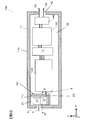
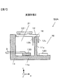
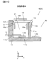
- FIG. 2 is a schematic plan view of Embodiment 1 of the power conversion device of the present invention
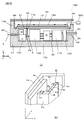
- FIG. 3A is a schematic cross-sectional view of the power conversion device illustrated in FIG. 2,
- FIG. Is a perspective view of the vicinity of the filter housing portion.
- the x direction, the y direction, and the z direction are as illustrated.
- Embodiment 1 of the present invention uses a DC-DC converter 100 as an example of a power conversion device.
- a DC-DC converter 100 that is a power converter includes a casing 11 and a case lid 14 that is fixed to the casing 11 by a fixing means (not shown) such as a fastening member.
- the housing 11 and the case lid 14 are made of metal such as aluminum die cast, for example.
- the casing 11 is electrically connected to the body or chassis of the automobile on which the DC-DC converter 100 is mounted, and the ground potential is the same as that of the vehicle body.
- the casing 11 has a substantially rectangular shape in plan view, and as shown in FIG. 3A, the casing 11 is formed substantially perpendicular to the bottom 11a. It has a peripheral side wall 11b and is formed in a box shape.
- the casing 11 is formed with a first partition wall 11c extending substantially perpendicular to the bottom portion 11a.
- the first partition wall 11 c is integrally formed with the housing 11.
- the first partition wall 11c is formed in a substantially L shape at one corner portion of the peripheral side wall 11b, and has a rectangular filter storage portion together with the peripheral side wall 11b at the corner portion. 31 is formed.
- the filter storage unit 31 stores an inductor Lf and a filter capacitor Cf that constitute the filter circuit unit 130. Further, an output terminal (not shown) connected to the filter circuit unit 130 is accommodated. An output bus bar 3 is connected to the output terminal, and the output bus bar 3 extends to the outside from an opening 41 formed in the peripheral side wall 11b.
- a space excluding the filter storage portion 31 of the housing 11 is a conversion circuit portion storage portion 32.
- the conversion circuit unit storage unit 32 stores a high voltage switching circuit unit 110, a low voltage switching circuit unit 120, a transformer Tr, and an input side filter circuit unit 140.
- the filter circuit unit 140 is provided with an input terminal (not shown), and input DC bus bars 2a and 2b are connected to the input terminal.
- the DC bus bars 2a and 2b are connected to an opening 42 formed in the peripheral side wall 11b. It is extended outside.
- a shield member (not shown) is interposed between the bus bar 3 and the opening 41, and between the DC bus bars 2a, 2b and the opening 42 to block electromagnetic noise from the outside. It is structured.
- a stepped portion 44 is formed on the inner surface of the peripheral side wall 11 b of the housing 11.
- the step portion 44 is formed at a position higher than any of the components arranged in the housing 11, and the base plate 12 is placed on the step portion 44.
- a control circuit board 151 is disposed on the base plate 12.
- the control circuit board 151 is fixed to the base plate 12 by a fastening member or the like.
- the case lid 14 is disposed on the control circuit board 151.
- the switching elements H1 to H4 are thermally coupled to the bottom 11a of the housing 11.
- the bottom 11a of the housing 11 is thermally coupled to a cooling flow path component having a cooling flow path for a coolant such as cooling water, and the switching elements H1 to H4 are connected via the housing 11. It is cooled by the cooling flow path component.
- This cooling structure is the same for other heat generating members such as the switching elements S1, S2, S3, S4 and the transformer Tr constituting the low voltage switching circuit unit 120.
- the filter circuit section 130 is electrically connected to the low voltage switching circuit section 120 by a connection bus bar 5 that passes through the opening 43 provided in the first partition wall 11c.
- a connection bus bar 5 that passes through the opening 43 provided in the first partition wall 11c.
- the inductor Lf disposed in the filter housing portion 31, that is, the one end surface of the ferrite core is disposed in close contact with the first partition wall 11c, The opening 43 is blocked. Therefore, electromagnetic noise is not propagated into the filter housing portion 31 through the opening 43.
- the control circuit board 151 is connected with a low-electric power source 500.
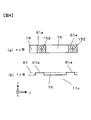
- FIG. 4A and 4B are enlarged views of the first partition wall shown in FIG. 2, and FIG. 4A is a plan view showing a part of the upper surface of the first partition wall 11c.
- 4 (b) is a side view of FIG. 4 (a) viewed from the x direction.
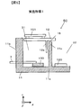
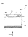
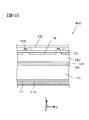
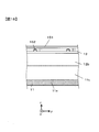
- 5 is a cross-sectional view taken along the line VV of FIG. 2, and
- FIG. 6 is a side view of FIG. 5 viewed from the x direction.
- a recess 16 is formed in the upper surface 61 of the first partition wall 11c.
- the upper surface 61 is provided with a plurality of attachment portions 61 a protruding upward (Z direction) with respect to the recess 16 and separated by the recess 16.
- the base plate 12 is fastened and fixed to the mounting portion 61a by a fastening member 152 such as a screw (see FIGS. 4 and 6).
- the base plate 12 and the first partition 11 c are electrically connected by being fastened by a fastening member 152.
- the upper part of the filter storage unit 31 is covered with the base plate 12.
- a control circuit board 151 having a control circuit unit is fixed to a region corresponding to the filter storage unit 31 on the upper surface of the base plate 12 by a fastening member.
- the fastening member connects the ground pattern (not shown) of the control circuit unit to the base plate 12.
- the recess 16 of the first partition 11c forms a gap between the first partition 11c and the base plate 12.
- FIG. 4A the illustration of the base plate 12 is omitted, and the relationship between the fastening member 152 and the mounting portion of the first partition 11c is clarified.
- the base plate 12 is integrally formed with a second partition 12b along the first partition 11c.
- the second partition 12b is illustrated by a two-dot chain line in FIG.
- the second partition wall 12b is disposed between the first partition wall 11c and the filter circuit unit 130 in the filter storage unit 31, and the first partition wall 11b is slightly spaced from the first partition wall 11c. It is formed along the entire length of the partition wall 11c.
- the second partition 12b extends from the bottom surface of the base plate 12 toward the bottom 11a of the housing 11 to the middle of the first partition 11c.
- the length of the second partition 12b in the z direction that is, the vertical direction is shorter than the length of the first partition 11c in the z direction.
- the vertical length of the second partition wall 12b needs to be at least larger than the depth of the recess 16 of the first partition wall 11c.
- the length of the second partition wall 12b in the vertical direction is desirably increased as long as the arrangement of the constituent members of the filter circuit unit 130 is not hindered.
- the electromagnetic noise propagation reduction structure 50 illustrated in FIG. 2 includes the first partition wall 11c and the second partition wall 12b. Next, the operation of the electromagnetic noise propagation reduction structure 50 will be described.
- the electromagnetic noise radiated from the low voltage switching circuit unit 120 is absorbed by the first partition 11c. However, a part of the electromagnetic noise enters the filter housing part 31 from the recess 16 provided in the first partition wall 11c.
- the electromagnetic noise is attenuated depending on the width and length of the gap serving as a propagation path of the electromagnetic noise.
- the length of the gap serving as the propagation path of electromagnetic noise is the thickness of the first partition wall 11c, in other words, In this case, only the length in the x direction or the y direction is obtained.
- the second partition wall 12b is formed adjacent to the first partition wall 11c.
- the length of the gap serving as an electromagnetic noise propagation path is apparently increased by the length in which the first partition 11c and the second partition 12b overlap. For this reason, compared with the structure partitioned only by the 1st partition 11c, the reduction effect of electromagnetic noise can be enlarged.
- the housing 11 is preferably grounded to the vehicle body.
- the second partition 12 b can also be disposed between the first partition 11 c and the low-voltage switching circuit unit 120 in the conversion circuit unit storage unit 32.
- electromagnetic noise radiated from the low voltage switching circuit unit 120 is obtained.
- it is directly absorbed by the second partition 12b before the first partition 11c and propagates to the base plate 12.
- electromagnetic noise propagates to the control circuit unit provided on the control circuit board 151 via the base plate 12.
- the vertical length of the second side wall 12b disposed between the first partition 11c and the low voltage switching circuit unit 120 cannot be increased so much. In other words, the length of the gap that becomes the propagation path of electromagnetic noise cannot be made too long.
- Embodiment 1 of the present invention in which the second partition wall 12b is disposed between the first partition wall 11c and the filter circuit unit 130, there is a concern about electromagnetic coupling with other circuits such as a comparison structure. Absent. Therefore, the length of the gap serving as the propagation path of electromagnetic noise can be made sufficiently long, and the effect of reducing propagation of electromagnetic noise can be increased.
- the reason for forming the recess 16 in the upper surface 61 of the first partition wall 11c will be described.
- the upper surface 61 of the first partition 11c is fastened in surface contact with the base plate 12. For this reason, there is a possibility that the base plate 12 and the upper surface 61 of the first partition wall 11c are abutted against each other or rubbed and worn by external vibration or impact, and metal powder may be generated.
- the generation of metal powder due to wear may cause problems such as a short circuit of the circuit portion.
- the concave portion 16 is formed in advance on the upper surface 61 of the first partition wall 11c.
- the structure in which the recess 16 is not formed on the upper surface 61 of the first partition wall 11c It is good.
- the DC-DC converter 100 has the following effects.
- the second partition wall 12 b provided on the metal base plate 12 is electrically and mechanically fixed to the first partition wall 11 c provided on the metal housing 11 by the fastening member 152.
- the second partition 12b is formed over the entire length along the first partition 11c with a slight gap from the first partition 11c. For this reason, the length of the propagation path of electromagnetic noise becomes long, and the effect of reducing electromagnetic noise can be increased.
- the second partition wall 12 b is disposed between the low voltage switching circuit unit 120 and the filter circuit unit 130. For this reason, only the part of the electromagnetic noise radiated from the low voltage switching circuit unit 120 that penetrates from the recess 16 that is the gap between the first partition 11c and the base plate 12 is propagated to the second partition 12b. The Therefore, the amount of electromagnetic noise absorbed by the base plate 12 is smaller than the structure in which the second partition is disposed closer to the low voltage switching circuit unit 120 than the first partition 11c. That is, there is almost no influence on other circuits via the base plate 12. For this reason, the length of the propagation path of electromagnetic noise can be sufficiently increased by the second partition wall 12b and the first partition wall 11c, and a large electromagnetic noise reduction effect can be obtained.
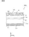
- FIG. 7 is a cross-sectional view showing Embodiment 2 of the electromagnetic noise propagation reducing structure of the present invention
- FIG. 8 is a side view of FIG. 7 viewed from the x direction. 7 and 8 correspond to FIGS. 5 and 6 of the first embodiment, respectively.
- the DC-DC converter 100 according to the second embodiment includes an electromagnetic noise propagation reduction structure 50A.
- the electromagnetic noise propagation reduction structure 50A further includes a third partition wall 12c with respect to the electromagnetic noise propagation reduction structure 50 of the first embodiment. That is, the base plate 12 of the second embodiment has a structure in which the third partition 12c is integrally formed with the second partition 12b.
- the second partition wall 12b is disposed between the first partition wall 11c and the filter circuit unit 130.
- the third partition wall 12 c is disposed between the first partition wall 11 c and the low voltage switching circuit unit 120.
- the third partition wall 12c is formed along the entire length of the first partition wall 11c with a slight gap from the first partition wall 11c.
- the third partition wall 12c extends toward the bottom 11a of the bottom casing 11 of the base plate 12 up to the middle of the first partition wall 11c.
- the vertical length of the third partition wall 12c is shorter than that of the second partition wall 12b.
- the electromagnetic noise propagation reduction structure 50A of the second embodiment includes the first partition 11c and the third partition 12c, the electromagnetic noise propagation path is longer than that of the electromagnetic noise propagation reduction structure 50 of the first embodiment. ing. Therefore, the electromagnetic noise reduction effect can be further increased.
- the vertical length of the third partition 12c is made shorter than that of the second partition 12b.
- the third partition 12c and the second partition 12b can have substantially the same vertical length.
- the vertical length of the second partition wall 12b may be shorter than that of the third partition wall 12c because of the layout of the filter circuit unit 130 stored in the filter storage unit 31.
- FIG. 9 is a cross-sectional view showing Embodiment 3 of the electromagnetic noise propagation reduction structure of the present invention
- FIG. 10 is a side view of FIG. 9 viewed from the x direction.
- the DC-DC converter 100 shown in the third embodiment includes an electromagnetic noise propagation reduction structure 50B.
- the electromagnetic noise propagation reduction structure 50 ⁇ / b> B is formed in the vicinity of the inner surface of the peripheral side wall 11 b of the housing 11 and the side end surface 62 of the base plate 12.
- the filter storage portion 31 aligns one corner portion of the partition wall 11c at one of the four corner portions of the rectangular housing 11. And concluded.
- a gap 17 is formed between the inner surface of the peripheral side wall 11b of the housing 11 and the side end surface 62 of the base plate 12 due to tolerances and variations in mounting. Is done.
- 4th partition 12d extended toward the bottom part 11a of the base board 12 is integrally molded by the bottom face of the location facing the surrounding side wall 11b of the base board 12. As shown in FIG.
- the fourth partition wall 12d is formed over the entire length of the filter storage portion 31 along the inner surface of the peripheral side wall 11b with a slight gap from the inner surface of the peripheral side wall 11b of the housing 11.
- the fourth partition 12d extends toward the bottom 11a of the housing 11 up to the middle of the height of the peripheral side wall 11b.
- the electromagnetic noise propagation reduction structure 50B that increases the length of the propagation path of electromagnetic noise is formed by the peripheral side wall 11b of the housing 11 and the fourth partition wall 12d of the base plate 12.
- This electromagnetic noise propagation reducing structure 50B suppresses electromagnetic noise propagating to the filter circuit unit 130 through the gap 17.
- Other structures in the third embodiment are the same as those in the first embodiment, and corresponding members and parts are denoted by the same reference numerals and description thereof is omitted.
- the DC-DC converter 100 of the third embodiment also has an effect of reducing electromagnetic noise propagated to the filter circuit unit 130, as in the first embodiment.
- the third embodiment is particularly suitable when electric noise propagated from the peripheral side wall 11b of the housing 11 and the side end face 62 of the base plate 12 is large.
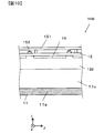
- FIG. 11 is a sectional view showing Embodiment 4 of the electromagnetic noise propagation reducing structure of the present invention
- FIG. 12 is a side view of FIG. 11 viewed from the x direction.
- the DC-DC converter 100 according to the fourth embodiment includes an electromagnetic noise propagation reduction structure 50C.
- the electromagnetic noise propagation reduction structure 50C has a structure in which the electromagnetic noise propagation reduction structure 50A of the second embodiment and the electromagnetic noise propagation reduction structure 50B of the third embodiment are combined.
- the base plate 12 has a structure in which the second partition 12b, the third partition 12c, and the fourth partition 12d are integrally formed.
- Other structures of the fourth embodiment are the same as those of the first embodiment, and corresponding members and parts are denoted by the same reference numerals and description thereof is omitted. Since the fourth embodiment has the effects of the second and third embodiments, the electromagnetic noise reduction effect can be further increased.
- FIG. 13 is a cross-sectional view showing Embodiment 5 of the electromagnetic noise propagation reduction structure of the present invention
- FIG. 14 is a side view of FIG. 13 viewed from the x direction.
- the DC-DC converter 100 according to the fifth embodiment includes an electromagnetic noise propagation reduction structure 50D.
- the electromagnetic noise propagation reduction structure 50D includes a first partition wall 11c, a fifth partition wall 11d, and a second partition wall 12b and a fourth partition wall 12d that are integrally formed with the base plate 12, respectively. ing.
- the fifth partition wall 11d is disposed between the second partition wall 12b and the filter circuit unit 130.
- the fifth partition 11d has a structure similar to that of the first partition 11c. That is, the concave portion 16 and the attachment portion 61a (see FIG. 4B) are formed on the upper surface of the fifth partition 11d.
- the base plate 12 is fastened to the attachment portion 61a of the fifth partition wall 11d by the fastening member 152.
- Other structures in the fifth embodiment are the same as those in the first embodiment, and corresponding members and parts are denoted by the same reference numerals and description thereof is omitted.
- the electromagnetic noise propagation reduction structure 50D of the fifth embodiment has a structure in which the third partition 12c of the fourth embodiment is replaced with a fifth partition 11d. That is, in the fourth embodiment, the third partition wall 12c is disposed closer to the low voltage switching circuit unit 120 than the first partition wall 11c, whereas in the fifth embodiment, the fifth partition wall 11d includes the first partition wall 12c. It arrange
- the possibility that the electromagnetic noise absorbed by the electromagnetic noise propagation reducing structure 50D is electromagnetically coupled to other circuits is smaller.
- the propagation path of electromagnetic noise can be made longer, so that the effect of suppressing electromagnetic noise can be further increased than in the fourth embodiment.
- FIG. 15 is a sectional view showing Embodiment 6 of the electromagnetic noise propagation reducing structure of the present invention
- FIG. 16 is a side view of FIG. 15 viewed from the x direction.
- the DC-DC converter 100 according to the sixth embodiment includes an electromagnetic noise propagation reduction structure 50E.
- the electromagnetic noise propagation reduction structure 50E is similar to the electromagnetic noise propagation reduction structure 50 of the first embodiment.
- the electromagnetic noise propagation reducing structure 50E is different from the electromagnetic noise propagation reducing structure 50 of the first embodiment in that the concave portion 16 is not formed on the upper surface 61 of the first partition wall 11c.
- the recess 16 of the first partition wall 11c is abutted against or rubbed with each other when the base plate 12 and the upper surface 61 of the second partition wall 12b are subjected to vibration or impact. It is formed to prevent wear and generation of metal powder.
- the DC-DC converter 100 is installed in an environment that is hardly subjected to vibration or impact, it is not necessary to form the recess 16 in the first partition wall 11c.
- Other structures of the sixth embodiment are the same as those of the first embodiment, and corresponding members and parts are denoted by the same reference numerals, and description thereof is omitted.
- Electromagnetic noise propagates in the filter housing 31 from this gap. However, since the propagation path of electromagnetic noise is long formed by the first partition wall 11c and the second partition wall 12b, the propagation of electromagnetic noise is suppressed.
- the structure where the recessed part 16 is not formed in the 1st partition 11c was illustrated as a structure applied to the electromagnetic noise propagation reduction structure 50 of Embodiment 1.
- FIG. a structure in which the recess 16 is not formed in the first partition 11c can be applied to the electromagnetic noise propagation reduction structures 50B to 50D of the second to fifth embodiments.
- FIG. 17 is sectional drawing which shows Embodiment 7 of the power converter device of this invention.
- a power conversion device 100A shown in FIG. 17 includes a DC-DC converter circuit 100 and an inverter circuit 200 housed in the housing 11.
- the inverter circuit 200 includes a plurality of switching elements formed of, for example, IGBT, and constitutes an inverter together with the capacitor module. The inverter converts the DC high voltage output of the high voltage storage battery into AC high voltage to drive the motor.
- the housing 11 is integrally formed with a partition wall 71 extending in the x direction, which is the longitudinal direction, in the middle of the y direction, that is, the width direction.
- the partition wall 71 is connected to one side wall 72 of the pair of side walls 72 and 73 extending in the y direction of the peripheral side wall 11 b, and is separated from the other side wall 73.
- An opening 74 is formed in the space between the partition wall 71 and the other side wall 73.
- the inverter circuit 200 is connected to the DC-DC converter 100 by DC bus bars 2 a and 2 b inserted through the opening 74.
- one of the electromagnetic noise propagation reducing structures 50 and 50A to 50E of the first to sixth embodiments is formed at one corner of the casing 11. . Therefore, as described in the first to sixth embodiments, the electromagnetic noise radiated from the DC-DC converter 100 and the inverter circuit 200 is transmitted to the filter circuit unit 130 on the output side by the electromagnetic noise propagation reduction structures 50 and 50A to 50E. Propagation is suppressed.
- the power conversion device is a power conversion device 100A having a structure in which a DC-DC converter 100 and an inverter circuit 200 are housed in a metal casing 11.
- Example 1 the electromagnetic noise propagation reduction structure 50 illustrated in FIG.
- Example 2 the electromagnetic noise propagation reduction structure 50A illustrated in FIG.
- Example 3 the electromagnetic noise propagation reduction structure 50B illustrated in FIG.
- Example 4 the electromagnetic noise propagation reduction structure 50C illustrated in FIG.
- an electromagnetic noise propagation reduction structure in which a partition wall is integrally formed on the base plate 12 on the low voltage switching circuit portion 120 side than the first partition wall 11c (see the comparative example shown in FIG. 18) is manufactured. did.
- the measurement reference structure was a structure having only the first partition wall in the housing 11 (see the measurement reference structure in FIG. 18).
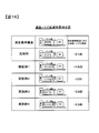
- FIG. 18 shows the results of measuring the increase and decrease of electromagnetic noise in each of Examples 1 to 4 and the comparative example with respect to the measurement reference structure.
- the electromagnetic noise with respect to the measurement reference structure was only reduced by 0.7 dB in the comparative example.
- the electromagnetic noise was reduced by 1.8 dB, 2.0 dB, 3.5 dB, and 6.2 dB, respectively.
- the first partition 11 c is exemplified as a structure integrally formed with the housing 11.
- the first partition 11c may be formed as a separate member from the casing 11 and joined by welding or the like.
- a groove is formed in one of the housing 11 and the first partition wall 11c, and a protrusion is provided on the other, and both members are integrated by shrink fitting or cold fitting, or the groove and the protrusion are fitted.
- the fastening member may be used for fastening.
- the groove and the protrusion are integrated by shrink fitting or cold fitting, or the groove and the protrusion are fitted. In the state, it may be fastened by a fastening member.
- the filter storage part 31 was formed in the corner part of the housing
- the filter housing part 31 is formed so that the peripheral side wall 11b is formed in a U shape in plan view, and the opening is closed by the U-shaped opening.
- the partition wall 11c is formed.
- the first partition 11c is linear, and the electromagnetic noise propagation reduction structure may be formed linearly along the first partition 11c.
- the first partition 11 c may be formed in a U shape in plan view, and the U-shaped opening may be closed by the side wall of the housing 11. it can.
- the electromagnetic noise propagation reduction structure is preferably formed in a U shape along the first partition 11c.
- the first partition 11 c can be formed in a frame shape inside the peripheral side wall 11 b of the housing 11.
- the electromagnetic noise propagation reduction structure is preferably formed in a frame shape along the first partition wall 11c.
- the ground pattern of the control circuit portion formed on the control circuit board 151 is exemplified as a structure in which the base plate 12 is fixed to the fastening member 152 and has the same potential.
- the ground pattern of the control circuit unit may be connected to the base plate 12 via a capacitor.
- the DC-DC converter 100 and the inverter 200 are illustrated as active circuits that radiate noise.
- the present invention is not limited to this, and can be applied to other power conversion devices.
- the present invention is not limited to the above embodiment.
- the active circuit unit and the filter circuit unit What is necessary is just to provide the base plate which has the housing
- the housing and the base plate may be formed from a conductive material, and are not limited to metal.
Landscapes
- Engineering & Computer Science (AREA)
- Power Engineering (AREA)
- Microelectronics & Electronic Packaging (AREA)
- Physics & Mathematics (AREA)
- Electromagnetism (AREA)
- Dc-Dc Converters (AREA)
- Shielding Devices Or Components To Electric Or Magnetic Fields (AREA)
Abstract
電力変換装置は、ノイズを放射する能動回路部と、出力側のフィルタ回路部と、能動回路部とフィルタ回路部とをそれぞれ収納する第1の空間および第2の空間を有する筐体と、少なくとも第1の空間を覆うように設けられ、筐体と電気的に接続されるベース板とを備え、筐体は、第1の空間と第2の空間とを区画する第1の隔壁を有し、ベース板は、第1の空間を覆って配置され、かつ、第1の隔壁に沿う第2の隔壁を有し、第2の隔壁は、第1の空間内においてフィルタ回路部と第1の隔壁との間に配置されている。
Description
本発明は、例えば、DC-DCコンバータまたはインバータ等の電力変換装置に関する。
ハイブリッド車やプラグインハイブリッド車、電気自動車などの車両には、動力駆動用の高電圧蓄電池と、高電圧蓄電池の直流高電圧出力を交流高電圧出力に電力変換してモータを駆動するためのインバータ装置と、高電圧蓄電池の直流高電圧出力を直流低電圧出力に変換して車両のライトやラジオなどの低電圧負荷へ電力供給を行うDC-DCコンバータ装置等が搭載されている。
DC-DCコンバータ装置は、直流高電圧を交流高電圧に変換する高電圧スイッチング回路、交流高電圧を交流低電圧に変換するトランス、交流低電圧を直流低電圧に変換する低電圧スイッチング回路、DC-DCコンバータ装置の外部へのノイズ伝導を低減させるフィルタ回路、スイッチング回路の制御信号を生成する制御回路を備えている。DC-DCコンバータ装置は、スイッチング回路およびトランスから漏れる電磁ノイズが、フィルタ回路や制御回路に伝播して電磁結合する可能性があるという課題を有している。
電磁ノイズの伝播を抑制する下記の構造が知られている。
金属製の筐体に、出力フィルタを、スイッチング素子を有する昇圧・高圧回路部からシールドするためのシールド壁を設け、シールド壁の上面に金属製のベース板を締結する。この構造によれば、スイッチング素子からの放射ノイズがシールド壁で吸収され、出力フィルタに重畳される電磁ノイズを低減することができると記載されている。さらに、出力フィルタとスイッチング素子とをシールドする第1のシールド壁を設けると共に、ベース板に、出力フィルタと、出力端子およびバスバとを分離する第2のシールド壁を設けた構造が示されている。第2のシールド壁は、出力フィルタと出力端子との間に配置されており、出力フィルタは、第1のシールド壁と第2のシールド壁との間に配置されている(例えば、特許文献1の図9参照)。
金属製の筐体に、出力フィルタを、スイッチング素子を有する昇圧・高圧回路部からシールドするためのシールド壁を設け、シールド壁の上面に金属製のベース板を締結する。この構造によれば、スイッチング素子からの放射ノイズがシールド壁で吸収され、出力フィルタに重畳される電磁ノイズを低減することができると記載されている。さらに、出力フィルタとスイッチング素子とをシールドする第1のシールド壁を設けると共に、ベース板に、出力フィルタと、出力端子およびバスバとを分離する第2のシールド壁を設けた構造が示されている。第2のシールド壁は、出力フィルタと出力端子との間に配置されており、出力フィルタは、第1のシールド壁と第2のシールド壁との間に配置されている(例えば、特許文献1の図9参照)。
金属製の筐体に形成したシールド壁と金属製のベース板とを締結するだけの構造では、シールド壁とベース板との隙間を介して出力フィルタに伝播される電磁ノイズを十分に抑えることはできない。また、ベース板に、出力フィルタと、出力端子およびバスバとを分離する第2のシールド壁を設けたとしても、出力フィルタは、第1のシールド壁と第2のシールド壁との間に配置されているので、第1のシールド壁とベース板との隙間を介して出力フィルタに伝播される電磁ノイズを抑えることはできない。
本発明の一の態様によると、電力変換装置は、ノイズを放射する能動回路部と、出力側のフィルタ回路部と、能動回路部とフィルタ回路部とをそれぞれ収納する第1の空間および第2の空間を有する筐体と、少なくとも第1の空間を覆うように設けられ、筐体と電気的に接続されるベース板とを備え、筐体は、第1の空間と第2の空間とを区画する第1の隔壁を有し、ベース板は、第1の空間を覆って配置され、かつ、第1の隔壁に沿う第2の隔壁を有し、第2の隔壁は、第1の空間内においてフィルタ回路部と第1の隔壁との間に配置されている。
本発明の他の態様によると、電力変換装置は、DC-DCコンバータ回路と、DC-DCコンバータ回路に接続された出力側のフィルタ回路部と、インバータ回路と、DC-DCコンバータ回路と、フィルタ回路部と、インバータ回路とを収納する金属製の筐体と、金属製の筐体と電気的に接続される金属製のベース板とを備え、筐体は、DC-DCコンバータ回路およびインバータ回路からフィルタ回路部をシールドする第1の筐体側隔壁およびフィルタ回路部の周囲に配置された側壁を有し、筐体は、第1の筐体側隔壁と筐体の側壁とで区画され、フィルタ回路部が収納される第1の空間を有し、ベース板は、第1の空間を覆って配置され、かつ、側壁の内面に沿って形成され、フィルタ回路部側に延出された第1のベース板側隔壁を有する。
本発明の他の態様によると、電力変換装置は、DC-DCコンバータ回路と、DC-DCコンバータ回路に接続された出力側のフィルタ回路部と、インバータ回路と、DC-DCコンバータ回路と、フィルタ回路部と、インバータ回路とを収納する金属製の筐体と、金属製の筐体と電気的に接続される金属製のベース板とを備え、筐体は、DC-DCコンバータ回路およびインバータ回路からフィルタ回路部をシールドする第1の筐体側隔壁およびフィルタ回路部の周囲に配置された側壁を有し、筐体は、第1の筐体側隔壁と筐体の側壁とで区画され、フィルタ回路部が収納される第1の空間を有し、ベース板は、第1の空間を覆って配置され、かつ、側壁の内面に沿って形成され、フィルタ回路部側に延出された第1のベース板側隔壁を有する。
本発明によれば、ノイズ発生回路部からフィルタ回路部に伝播されるノイズの低減を図ることができる。
-実施形態1-
電動モータによって駆動動力を得る自動車(モータのみを駆動動力源とする自動車、補助的駆動動力としてモータを使用する自動車いずれも含む)へ搭載されるDC-DCコンバータは一般的に、高電圧スイッチング回路・トランス・低電圧側整流回路・制御回路を最小基本構成とする。DC―DCコンバータは一般的に、電動モータを駆動するための数百Vの直流高電圧電源の供給を受け、高電圧スイッチング回路において、制御回路より供給されるスイッチング信号を受けて、スイッチング動作を行い交流高電圧化し、トランスにより交流高電圧を交流低電圧へ電圧変換を行い、その後、整流・直流化して、車両補機類に十数Vの直流低電圧電源を供給する機能をもつ。
電動モータによって駆動動力を得る自動車(モータのみを駆動動力源とする自動車、補助的駆動動力としてモータを使用する自動車いずれも含む)へ搭載されるDC-DCコンバータは一般的に、高電圧スイッチング回路・トランス・低電圧側整流回路・制御回路を最小基本構成とする。DC―DCコンバータは一般的に、電動モータを駆動するための数百Vの直流高電圧電源の供給を受け、高電圧スイッチング回路において、制御回路より供給されるスイッチング信号を受けて、スイッチング動作を行い交流高電圧化し、トランスにより交流高電圧を交流低電圧へ電圧変換を行い、その後、整流・直流化して、車両補機類に十数Vの直流低電圧電源を供給する機能をもつ。
制御回路は直流-交流変換の際のスイッチング動作を演算・制御するための回路であり、上記両電源間の電力状態に応じ、または外部からの通信指令によって、最適なスイッチング期間を算出し制御する回路である。自動車に搭載される電力変換を行う機器においては、安全上の理由から、高電圧系回路と低電圧系回路は、電気的な絶縁を必要とする。筐体が導電性金属で構成される場合、多くは筐体電位と車両ボディを同電位とし、低電圧系の基準電位(いわゆる筐体接地=グラウンド電位)としている。ただし、車載という条件から、小型化・一体ユニット化要求が強く、高電圧系回路と低電圧系回路は、車両ボディと同一電位とした筐体内に一括収納して、一体型ユニットを構成し、電力変換機能を達成する場合がほとんどである。なお、DC-DCコンバータの一般的な電力変換特性として、高電圧系回路は電圧が高いが比較的小電流(~30A程度)、低電圧系回路は比較的電圧が低いが大電流(~200A程度)という特性を持つ。
これら高電圧系回路と低電圧系回路を、同一筐体内に収納する場合、筐体内配置における各々の回路系の前記のような電力変換特性・相互位置関係及び配置距離・筐体およびフレームの配置状況などにより、高電圧系回路の電圧依存性ノイズおよび低電圧系の電流依存性ノイズが他回路系に電磁結合するといった現象が発生する。この結果、DC-DCコンバータとしての基本機能である電力変換機能の誤動作や、ノイズ規制値(各国法規制及び顧客要求仕様)を満たせないといった問題が発生する。
これらの問題を改善するためには、回路の見直しはもちろんであるが、新たにノイズ対策用構造部品として、シールドケースや導通強化部品を追加する必要が生じ、結果、製品としてコストアップや体積・重量の増加を招く。
以下、図1~6を参照して本発明の実施形態1を説明する。
なお、各図において同一要素については同一の符号を記し、重複する説明は省略する。
以下、図1~6を参照して本発明の実施形態1を説明する。
なお、各図において同一要素については同一の符号を記し、重複する説明は省略する。
(DC-DCコンバータの回路構成)
DC-DCコンバータ100について説明する。このDC-DCコンバータ100は高電圧バッテリから低電圧バッテリへの電力変換を行う装置であるが、一方向に限らず、両方向、即ち、直流高電圧電源から直流低電圧電源への変換、逆に直流低電圧電源から直流高電圧電源への変換を行うものも含む。図1はDC-DCコンバータ100の回路構成の一実施の形態を示す図である。
DC-DCコンバータ100について説明する。このDC-DCコンバータ100は高電圧バッテリから低電圧バッテリへの電力変換を行う装置であるが、一方向に限らず、両方向、即ち、直流高電圧電源から直流低電圧電源への変換、逆に直流低電圧電源から直流高電圧電源への変換を行うものも含む。図1はDC-DCコンバータ100の回路構成の一実施の形態を示す図である。
図1に示すように、本発明の一実施の形態として示すDC-DCコンバータ100は、高電圧スイッチング回路部110と、低電圧スイッチング回路部120と、出力側のフィルタ回路部130と、高電圧スイッチング回路部110と低電圧スイッチング回路部120との間に設けられたトランスTrと、入力側のフィルタ回路部140を備えている。高電圧スイッチング回路部110と低電圧スイッチング回路部120のスイッチング制御は制御回路基板151(図3、5等参照)上に構成された制御回路部により行われる。なお、制御回路基板151に回路形成された制御回路部は図1には図示されていない。
高電圧スイッチング回路部110は、Hブリッジ型スイッチング回路として接続されたMOSFET等で形成されたスイッチング素子H1~H4と、共振コイルLrと、平滑コンデンサCinを備える。平滑コンデンサCinは、Hブリッジ型スイッチング回路の入力側に配置され、高電圧スイッチング回路部110に入力される入力電流を平滑にする。なお、スイッチング素子H1~H4のゲート端子には図示しないゲート抵抗が接続されている。
図1の破線で囲った高電圧スイッチング回路部110は、高電圧スイッチング回路部110を構成するスイッチング素子H1~H4をHブリッジ接続する配線回路基板上に設けられる。また、この配線回路基板には、スイッチング素子H1~H4であるパワー半導体モジュール 、平滑コンデンサCin、および共振コイルLrを除くその他の電子部品が実装されるとともに、それらの配線パターンも設けられる。
低電圧スイッチング回路部120は、MOSFET等で形成される4つのスイッチング素子S1、S2、S3、S4と、コイルLoutと、コンデンサCc及びCoutを備えている。低電圧スイッチング回路部120は、同期整流方式による整流を行い、アクティブクランプ方式によりサージ吸収を実現し、回路部品の低耐圧化を図り、装置を小型化している。なお、低電圧整流回路部の構成は、上記同期整流方式と同じ必要はなく、ダイオード整流方式でも構わないし、アクティブクランプ方式の採否を問わない。
なお、MOSFET S1~S4のゲート端子には図示しないゲート抵抗が接続されている。
なお、MOSFET S1~S4のゲート端子には図示しないゲート抵抗が接続されている。
出力側のフィルタ回路部130は、インダクタLfおよびフィルタコンデンサCfを備えている。
なお、出力側のノイズフィルタ回路は図1に示すような回路構成に限定しない。当然、複数の素子を用いて実現しても構わない。
なお、出力側のノイズフィルタ回路は図1に示すような回路構成に限定しない。当然、複数の素子を用いて実現しても構わない。
図1の破線で囲った低電圧スイッチング回路部120は、スイッチング素子S1~S4を接続する配線が回路基板上に設けられる。また、この回路基板には、図1に示す電子部品のうちコイルLoutを除く電子部品が実装されるとともに、それらの配線パターンも設けられる。
制御回路基板151に回路形成された制御回路部(図示せず)は、高電圧スイッチング回路部110および低電圧スイッチング回路部120へ供給するスイッチング信号を生成し、且つDC-DCコンバータ100全体の動作制御を行う。
制御回路基板151に回路形成された制御回路部(図示せず)は、高電圧スイッチング回路部110および低電圧スイッチング回路部120へ供給するスイッチング信号を生成し、且つDC-DCコンバータ100全体の動作制御を行う。
入力側のフィルタ回路部140は、高電圧電源と平滑化コンデンサCinの間にコモンモードフィルタLcmnとコンデンサCyが備えられている。これにより、高電圧電源およびバッテリケーブルにコモンモードノイズが伝導することを防いでいる。フィルタ回路部130は、基本的にはコイル及びコンデンサで構成されるが、コンデンサのみで構成されるものでも構わない。なお、図1の回路は素子数を示すものではなく、回路記号例である。当然、複数の素子を用いて実現しても構わない。また、入力側のフィルタ回路部140は必ずしも必要ではなく、製品仕様に応じて採否を決めればよい。
次に、DC-DCコンバータ100の全体構造について説明する。
次に、DC-DCコンバータ100の全体構造について説明する。
(DC-DCコンバータの全体構造)
図2は、本発明の電力変換装置の実施形態1の模式的平面図であり、図3(a)は、図2に図示された電力変換装置の模式的断面図であり、図3(b)は、フィルタ収納部周辺の斜視図である。
なお、以下において、x方向、y方向およびz方向を図示の通りとする。
本発明の実施形態1は、電力変換装置としてDC-DCコンバータ100を例とする。
電力変換装置であるDC-DCコンバータ100は、筐体11および筐体11に締結部材等の固定手段(図示せず)により固定されるケース蓋14を備えている。図1に図示されたDC-DCコンバータ100の回路部品は、筐体11内に収容される。筐体11およびケース蓋14は、例えば、アルミダイキャスト等の金属により形成されている。筐体11はDC-DCコンバータ100が搭載される自動車のボディまたはシャーシに電気的に接続され、グラウンド電位は、車両ボディと同電位となっている。
筐体11は、図2に図示されるように、平面視でほぼ矩形形状を有し、図3(a)に図示されるように、底部11aと、この底部11aにほぼ垂直に形成された周側壁11bとを有し、ボックス状に形成されている。筐体11には、底部11aに対してほぼ垂直に延在された第1の隔壁11cが形成されている。第1の隔壁11cは、筐体11と一体成形されている。第1の隔壁11cは、図3(b)に示されるように、周側壁11bの1つのコーナー部に、ほぼL字形状に形成され、コーナー部における周側壁11bと共に、矩形形状のフィルタ収納部31を形成する。フィルタ収納部31には、フィルタ回路部130を構成するインダクタLfとフィルタコンデンサCfとが収納されている。また、フィルタ回路部130に接続された不図示の出力端子が収納されている。この出力端子には出力用のバスバ3が接続され、出力用のバスバ3は、周側壁11bに形成された開口41から外部に延出されている。
筐体11のフィルタ収納部31を除く空間は、変換用回路部収納部32となっている。変換用回路部収納部32には、高電圧スイッチング回路部110と、低電圧スイッチング回路部120と、トランスTrと、入力側のフィルタ回路部140とが収納されている。フィルタ回路部140には、不図示の入力端子が設けられ、この入力端子には入力用の直流バスバ2a、2bが接続され、直流バスバ2a、2bは、周側壁11bに形成された開口42から外部に延出されている。
なお、図示はしないが、バスバ3と開口41の間、および直流バスバ2a、2bと開口42との間には、不図示のシールド部材が介装されており、外部からの電磁ノイズを遮断する構造とされている。
なお、図示はしないが、バスバ3と開口41の間、および直流バスバ2a、2bと開口42との間には、不図示のシールド部材が介装されており、外部からの電磁ノイズを遮断する構造とされている。
図3(a)、(b)に図示されるように、筐体11の周側壁11bの内面には、段部44が形成されている。段部44は、筐体11内に配置される部品のいずれよりも高い位置に形成されており、この段部44上にベース板12が載置されている。ベース板12上に、制御回路基板151が配置されている。制御回路基板151は、締結部材等によりベース板12に固定されている。ケース蓋14は、制御回路基板151上に配置されている。
図示はしないが、スイッチング素子H1~H4は、筐体11の底部11aに熱結合されている。筐体11の底部11aは、図示はしないが、冷却水などの冷媒の冷却流路を備えた冷却流路構成部材に熱結合されており、スイッチング素子H1~H4は、筐体11を介して冷却流路構成部材によって冷却される。この冷却構造は、低電圧スイッチング回路部120を構成するスイッチング素子S1、S2、S3、S4やトランスTr等、他の発熱部材に対しても同様である。
フィルタ回路部130は、第1の隔壁11cに設けられた開口43を挿通する接続用のバスバ5により、低電圧スイッチング回路部120に電気的に接続されている。図2、図3(a)に図示されるように、フィルタ収納部31内に配置されたインダクタLf、すなわち、フェライトコアの一端面が第1の隔壁11cに密着した状態で配置されており、開口43を塞いでいる。従って、電磁ノイズが開口43を介してフィルタ収納部31内に伝播されることはない。なお、図3(a)に示されるように、制御回路基板151には、弱電系の電源500が接続されている。
(電磁ノイズ伝播低減構造)
図2の点線で囲まれた領域には、電磁ノイズ伝播低減構造50が設けられている。
図4(a)、(b)は図2に図示された第1の隔壁の拡大図であり、図4(a)は第1の隔壁11cの上面の一部を示す平面図であり、図4(b)は、図4(a)をx方向から観た側面図である。図5は、図2のV-V線断面図であり、図6は、図5をx方向から観た側面図である。
図3(b)および図4(a)、(b)に図示されるように、第1の隔壁11cの上面61には、凹部16が形成されている。換言すれば、上面61には、凹部16に対して上方(Z方向)に突き出す複数の取付部61aが、凹部16で分離して設けられている。
図2の点線で囲まれた領域には、電磁ノイズ伝播低減構造50が設けられている。
図4(a)、(b)は図2に図示された第1の隔壁の拡大図であり、図4(a)は第1の隔壁11cの上面の一部を示す平面図であり、図4(b)は、図4(a)をx方向から観た側面図である。図5は、図2のV-V線断面図であり、図6は、図5をx方向から観た側面図である。
図3(b)および図4(a)、(b)に図示されるように、第1の隔壁11cの上面61には、凹部16が形成されている。換言すれば、上面61には、凹部16に対して上方(Z方向)に突き出す複数の取付部61aが、凹部16で分離して設けられている。
ベース板12は、この取付部61aにねじ等の締結部材152(図4、図6参照)により締結され固定されている。ベース板12と第1の隔壁11cとは、締結部材152により締結されることにより電気的に接続されている。フィルタ収納部31の上部は、ベース板12により覆われる。図5に図示されるように、ベース板12の上面におけるフィルタ収納部31に対応する領域には、制御回路部を有する制御回路基板151が、締結部材により固定される。締結部材は、制御回路部の接地パターン(図示せず)をベース板12に接続する。
ベース板12と第1の隔壁11cとの締結構造において、第1の隔壁11cの凹部16は、第1の隔壁11cとベース板12との隙間を形成する。なお、図4(a)では、ベース板12の図示を省略して、締結部材152と第1の隔壁11cの取付部との関連を明確にしている。
図5に示すように、ベース板12には、第1の隔壁11cに沿う第2の隔壁12bが一体成形されている。第2の隔壁12bは、図3(b)では、二点鎖線により図示されている。第2の隔壁12bは、フィルタ収納部31内において、第1の隔壁11cとフィルタ回路部130との間に配置されており、第1の隔壁11cとわずかな隙間を存して、第1の隔壁11cの全長に沿って形成されている。第2の隔壁12bは、ベース板12の底面から筐体11の底部11aに向けて、第1の隔壁11cの中間まで延出されている。第2の隔壁12bのz方向、すなわち上下方向の長さは、第1の隔壁11cのz方向の長さよりも短い。第2の隔壁12bの上下方向の長さは、少なくとも、第1の隔壁11cの凹部16の深さより大きくする必要である。第2の隔壁12bの上下方向の長さは、フィルタ回路部130の構成部材の配置に支障がない限り、大きくすることが望ましい。
このように、図2に図示された電磁ノイズ伝播低減構造50は、第1の隔壁11cおよび第2の隔壁12bにより構成される。
次に、電磁ノイズ伝播低減構造50による作用について説明する。
このように、図2に図示された電磁ノイズ伝播低減構造50は、第1の隔壁11cおよび第2の隔壁12bにより構成される。
次に、電磁ノイズ伝播低減構造50による作用について説明する。
低電圧スイッチング回路部120から放射される電磁ノイズは、第1の隔壁11cにより吸収される。しかし、電磁ノイズの一部は、第1の隔壁11cに設けられた凹部16からフィルタ収納部31内に侵入する。電磁ノイズがフィルタ回路部130に伝播して電磁結合するとフィルタ性能が低下する恐れがある。電磁ノイズは、電磁ノイズの伝播経路となる隙間の幅および長さの大きさに依存して減衰する。フィルタ収納部31と変換用回路部収納部32とが第1の隔壁11cのみで区画されている場合、電磁ノイズの伝播経路となる隙間の長さは、第1の隔壁11cの厚さ、換言すればx方向またはy方向の長さのみである。本発明の実施形態1では、第1の隔壁11cに隣接して第2の隔壁12bを形成した。この構造では、電磁ノイズの伝播経路となる隙間の長さは、見掛け上、第1の隔壁11cと第2の隔壁12bとが重なる長さだけ長くなる。このため、第1の隔壁11cのみで区画されている構造に比し、電磁ノイズの低減効果を大きくすることができる。
なお、上述したように、筐体11は、車両ボディに接地することが好ましい。
なお、上述したように、筐体11は、車両ボディに接地することが好ましい。
ここで、第2の隔壁12bを、変換用回路部収納部32内において、第1の隔壁11cと低電圧スイッチング回路部120との間に配置することもできる。しかし、第2の隔壁12bを、第1の隔壁11cより低電圧スイッチング回路部120側に配置する構造(以下、「対比構造」とする)では、低電圧スイッチング回路部120から放射される電磁ノイズが、直接、第1の隔壁11cより手前の第2の隔壁12bに吸収されてベース板12に伝播する。
電磁ノイズが、第1の隔壁11cより手前の第2の隔壁12bに吸収されてベース板12に吸収された場合、ベース板12を介して制御回路基板151に設けられた制御回路部等に伝播するため、第1の隔壁11cを介して筐体11からグラウンドに落ちる場合に比し、制御回路部等、他の回路と電磁結合する恐れが高い。このため、対比構造においては、第1の隔壁11cと低電圧スイッチング回路部120との間に配置する第2の側壁12bの上下方向の長さをあまり大きくすることができない。つまり、電磁ノイズの伝播経路となる隙間の長さを余り長くすることができない。
電磁ノイズが、第1の隔壁11cより手前の第2の隔壁12bに吸収されてベース板12に吸収された場合、ベース板12を介して制御回路基板151に設けられた制御回路部等に伝播するため、第1の隔壁11cを介して筐体11からグラウンドに落ちる場合に比し、制御回路部等、他の回路と電磁結合する恐れが高い。このため、対比構造においては、第1の隔壁11cと低電圧スイッチング回路部120との間に配置する第2の側壁12bの上下方向の長さをあまり大きくすることができない。つまり、電磁ノイズの伝播経路となる隙間の長さを余り長くすることができない。
これに対し、第2の隔壁12bを、第1の隔壁11cとフィルタ回路部130との間に配置した本発明の実施形態1では、対比構造のような他の回路との電磁結合の懸念がない。従って、電磁ノイズの伝播経路となる隙間の長さを十分な長さにすることが可能であり、電磁ノイズの伝播の低減効果を大きくすることができる。
なお、第1の隔壁11cの上面61に凹部16を形成する理由について説明する。
第1の隔壁11cの上面61はベース板12と面接触して締結されている。このため、外部からの振動や衝撃により、ベース板12と第1の隔壁11cの上面61とが、相互に当接したり擦れたりして摩耗し、金属粉が発生する可能性がある。摩耗により金属粉が発生することは、回路部の短絡等の不具合を生じる恐れがある。
第1の隔壁11cの上面61に凹部16を設けることにより、第1の隔壁11cの取付部61aの面積は小さくなり、摩耗による金属粉の発生を抑制することができる。このため、前以て、第1の隔壁11cの上面61に凹部16を形成しておくのである。
しかし、DC-DCコンバータ100が、振動や衝撃をほとんど受けることが無いような環境下に設置されるならば、上記実施形態1において、第1の隔壁11cの上面61に凹部16を形成しない構造としてもよい。
以上説明したように、実施形態1のDC-DCコンバータ100によれば以下の効果を奏する。
(1)金属製の筐体11に設けた第1の隔壁11cに、金属製のベース板12に設けられた第2の隔壁12bを、締結部材152により電気的および機械的に固定した。第2の隔壁12bは、第1の隔壁11cと僅かな隙間を存して、第1の隔壁11cに沿って、その全長に亘って形成されている。このため、電磁ノイズの伝播経路の長さが長くなり、電磁ノイズの低減効果を大きくすることができる。
(1)金属製の筐体11に設けた第1の隔壁11cに、金属製のベース板12に設けられた第2の隔壁12bを、締結部材152により電気的および機械的に固定した。第2の隔壁12bは、第1の隔壁11cと僅かな隙間を存して、第1の隔壁11cに沿って、その全長に亘って形成されている。このため、電磁ノイズの伝播経路の長さが長くなり、電磁ノイズの低減効果を大きくすることができる。
(2)第2の隔壁12bが、低電圧スイッチング回路部120とフィルタ回路部130との間に配置されている。このため、第2の隔壁12bには、低電圧スイッチング回路部120から放射される電磁ノイズのうち、第1の隔壁11cとベース板12との隙間である凹部16から侵入する分のみが伝播される。従って、第2の隔壁が、第1の隔壁11cよりも低電圧スイッチング回路部120側に配置される構造に比し、ベース板12に吸収される電磁ノイズの量が少ない。つまり、ベース板12を介して他の回路が受ける影響はほとんどない。このため、第2の隔壁12bと第1の隔壁11cとにより、電磁ノイズの伝播経路の長さを十分に大きくして、大きな電磁ノイズ低減効果を得ることができる。
-実施形態2-
図7は、本発明の電磁ノイズ伝播低減構造の実施形態2を示す断面図であり、図8は、図7をx方向から観た側面図である。図7、図8は、それぞれ、実施形態1の図5、図6に対応する図である。
実施形態2のDC-DCコンバータ100は、電磁ノイズ伝播低減構造50Aを備えている。電磁ノイズ伝播低減構造50Aは、実施形態1の電磁ノイズ伝播低減構造50に対し、さらに、第3の隔壁12cを備えている。
すなわち、実施形態2のベース板12は、第2の隔壁12bと共に第3の隔壁12cが一体成形された構造を有する。
図7は、本発明の電磁ノイズ伝播低減構造の実施形態2を示す断面図であり、図8は、図7をx方向から観た側面図である。図7、図8は、それぞれ、実施形態1の図5、図6に対応する図である。
実施形態2のDC-DCコンバータ100は、電磁ノイズ伝播低減構造50Aを備えている。電磁ノイズ伝播低減構造50Aは、実施形態1の電磁ノイズ伝播低減構造50に対し、さらに、第3の隔壁12cを備えている。
すなわち、実施形態2のベース板12は、第2の隔壁12bと共に第3の隔壁12cが一体成形された構造を有する。
第2の隔壁12bは、実施形態1と同様、第1の隔壁11cとフィルタ回路部130との間に配置されている。第3の隔壁12cは、第1の隔壁11cと低電圧スイッチング回路部120との間に配置されている。第3の隔壁12cは、第1の隔壁11cとわずかな隙間を存して、第1の隔壁11cの全長に沿って形成されている。第3の隔壁12cは、ベース板12の底面筐体11の底部11aに向けて、第1の隔壁11cの中間まで延出されている。第3の隔壁12cの上下方向の長さは、第2の隔壁12bよりも短い。
実施形態2の他の構造は、実施形態1と同様であり、対応する部材、部位に同一の参照符号を付して、説明を省略する。
実施形態2の他の構造は、実施形態1と同様であり、対応する部材、部位に同一の参照符号を付して、説明を省略する。
実施形態2の電磁ノイズ伝播低減構造50Aでは、第1の隔壁11cと第3の隔壁12cを有するので、この分、電磁ノイズの伝播経路が実施形態1の電磁ノイズ伝播低減構造50よりも長くなっている。
従って、電磁ノイズの低減効果をより大きくすることができる。
従って、電磁ノイズの低減効果をより大きくすることができる。
なお、上述したように、第3の隔壁12cの上下方向の長さを大きくすると、ベース板12に吸収される電磁ノイズの量が増大するので、この長さを余り大きくすることはできない。このため、図7に示す例では、第3の隔壁12cの上下方向の長さを、第2の隔壁12bよりも短くしている。しかし、他の回路への影響が小さければ、第3の隔壁12cと第2の隔壁12bとは、上下方向の長さをほぼ同じにすることができる。また、フィルタ収納部31内に収納されるフィルタ回路部130のレイアウトの関係で、第2の隔壁12bの上下方向の長さを、第3の隔壁12cよりも短くしてもよい。
-実施形態3-
図9は、本発明の電磁ノイズ伝播低減構造の実施形態3を示す断面図であり、図10は、図9をx方向から観た側面図である。
実施形態3に示すDC-DCコンバータ100は、電磁ノイズ伝播低減構造50Bを備えている。
電磁ノイズ伝播低減構造50Bは、筐体11の周側壁11bの内面とベース板12の側端面62の近傍に形成されている。
図2、図3(b)に図示されるように、フィルタ収納部31は、矩形形状の筐体11の4つのコーナー部の内の1か所に、隔壁11cの1つのコーナー部を位置合わせして締結される。ベース板12を、隔壁11cに締結する際、筐体11の上記周側壁11bの内面とベース板12の上記側端面62との間には、公差や取付時のばらつきに起因する隙間17が形成される。
ベース板12の周側壁11bと対向する箇所の底面には、ベース板12の底部11aに向かって延出された第4の隔壁12dが一体成形されている。第4の隔壁12dは、筐体11の周側壁11bの内面とわずかな隙間を存して、周側壁11bの内面に沿って、フィルタ収納部31内の全長に亘って形成されている。第4の隔壁12dは、筐体11の底部11aに向けて、周側壁11bの高さの中間まで延出されている。
すなわち、筐体11の周側壁11bとベース板12の第4の隔壁12dにより、電磁ノイズの伝播経路の長さを長くする電磁ノイズ伝播低減構造50Bが形成されている。この電磁ノイズ伝播低減構造50Bにより隙間17を介してフィルタ回路部130に伝播される電磁ノイズが抑制される。
実施形態3における他の構造は、実施形態1と同様であり、対応する部材、部位に同一の符号を付して説明を省略する。
実施形態3における他の構造は、実施形態1と同様であり、対応する部材、部位に同一の符号を付して説明を省略する。
実施形態3のDC-DCコンバータ100も、実施形態1と同様、フィルタ回路部130に伝播される電磁ノイズを低減する効果を奏する。実施形態3は、特に、筐体11の周側壁11bとベース板12の側端面62から伝播される電ノイズが大きい場合に適する。
-実施形態4-
図11は、本発明の電磁ノイズ伝播低減構造の実施形態4を示す断面図であり、図12は、図11をx方向から観た側面図である。
実施形態4のDC-DCコンバータ100は、電磁ノイズ伝播低減構造50Cを備えている。電磁ノイズ伝播低減構造50Cは、実施形態2の電磁ノイズ伝播低減構造50Aと実施形態3の電磁ノイズ伝播低減構造50Bとを組み合わせた構造を有する。
図11は、本発明の電磁ノイズ伝播低減構造の実施形態4を示す断面図であり、図12は、図11をx方向から観た側面図である。
実施形態4のDC-DCコンバータ100は、電磁ノイズ伝播低減構造50Cを備えている。電磁ノイズ伝播低減構造50Cは、実施形態2の電磁ノイズ伝播低減構造50Aと実施形態3の電磁ノイズ伝播低減構造50Bとを組み合わせた構造を有する。
すなわち、ベース板12は、第2の隔壁12bと、第3の隔壁12cと、第4の隔壁12dとが一体成形された構造を有する。
実施形態4の他の構造は、実施形態1と同様であり、対応する部材、部位に同一の符号を付して説明を省略する。
実施形態4は、実施形態2および実施形態3の効果を有しているので、電磁ノイズの低減効果をさらに大きくすることができる。
実施形態4の他の構造は、実施形態1と同様であり、対応する部材、部位に同一の符号を付して説明を省略する。
実施形態4は、実施形態2および実施形態3の効果を有しているので、電磁ノイズの低減効果をさらに大きくすることができる。
-実施形態5-
図13は、本発明の電磁ノイズ伝播低減構造の実施形態5を示す断面図であり、図14は、図13をx方向から観た側面図である。
実施形態5のDC-DCコンバータ100は、電磁ノイズ伝播低減構造50Dを備えている。電磁ノイズ伝播低減構造50Dは、筐体11に一体成形された第1の隔壁11c、第5の隔壁11d、およびベース板12に一体成形された第2の隔壁12b、第4の隔壁12dを備えている。
図13は、本発明の電磁ノイズ伝播低減構造の実施形態5を示す断面図であり、図14は、図13をx方向から観た側面図である。
実施形態5のDC-DCコンバータ100は、電磁ノイズ伝播低減構造50Dを備えている。電磁ノイズ伝播低減構造50Dは、筐体11に一体成形された第1の隔壁11c、第5の隔壁11d、およびベース板12に一体成形された第2の隔壁12b、第4の隔壁12dを備えている。
第5の隔壁11dは、第2の隔壁12bとフィルタ回路部130との間に配置されている。第5の隔壁11dは、第1の隔壁11cと同様な構造を有している。すなわち、第5の隔壁11dの上面には凹部16および取付部61a(図4(b)参照)が形成されている。ベース板12は、締結部材152により第5の隔壁11dの取付部61aに締結される。
実施形態5における他の構造は、実施形態1と同様であり、対応する部材、部位に同一の符号を付して説明を省略する。
実施形態5における他の構造は、実施形態1と同様であり、対応する部材、部位に同一の符号を付して説明を省略する。
実施形態5の電磁ノイズ伝播低減構造50Dは、実施形態4の第3の隔壁12cを、第5の隔壁11dに置換したような構造となっている。すなわち、実施形態4では、第3の隔壁12cが第1の隔壁11cよりも低電圧スイッチング回路部120側に配置されているに対し、実施形態5では、第5の隔壁11dは、第1の隔壁11cよりもフィルタ回路部130側に配置されている。しかも、実施形態4では、第3の隔壁12cがベース板12に一体成形されているに対し、第5の隔壁11dは筐体11に一体成形されている。このため、実施形態4の電磁ノイズ伝播低減構造50Cに比し、電磁ノイズ伝播低減構造50Dにより吸収される電磁ノイズが他の回路と電磁結合する可能性がより小さい。これに伴って、電磁ノイズの伝播経路をより長くすることが可能となるので、実施形態4よりも、さらに、電磁ノイズの抑制効果を大きくすることができる。
-実施形態6-
図15は、本発明の電磁ノイズ伝播低減構造の実施形態6を示す断面図であり、図16は、図15をx方向から観た側面図である。
実施形態6のDC-DCコンバータ100は、電磁ノイズ伝播低減構造50Eを備えている。
電磁ノイズ伝播低減構造50Eは、実施形態1の電磁ノイズ伝播低減構造50と類似する。しかし、電磁ノイズ伝播低減構造50Eは、第1の隔壁11cには、その上面61に凹部16が形成されていない点で、実施形態1の電磁ノイズ伝播低減構造50と相違する。
実施形態1において説明した通り、第1の隔壁11cの凹部16は、ベース板12と第2の隔壁12bの上面61とが、振動や衝撃を受けた際に、相互に当接したり擦れたりして摩耗し、金属粉が発生することを防止するために形成される。しかし、DC-DCコンバータ100が、振動や衝撃をほとんど受けることが無いような環境下に設置されるならば、第1の隔壁11cに凹部16を形成する必要は無い。
実施形態6の他の構造は、実施形態1と同様であり、対応する部材、部位に同一の参照符号を付して、説明を省略する。
第1の隔壁11cの上面61に凹部16が形成されておらず、上面61が平坦であっても、上面61とベース板12の底面とが面接触する領域には、微小な隙間が存在する。この隙間から電磁ノイズがフィルタ収納部31内に伝播する。しかし、電磁ノイズの伝播経路は、第1の隔壁11cと第2の隔壁12bにより長く形成されているので、電磁ノイズの伝播は抑制される。
なお、上記では、第1の隔壁11cに凹部16が形成されない構造を、実施形態1の電磁ノイズ伝播低減構造50に適用した構造として例示した。しかし、第1の隔壁11cに凹部16が形成されない構造を、第2~第5の実施形態それぞれの電磁ノイズ伝播低減構造50B~50Dに適用することもできる。
-実施形態7-
図17は、本発明の電力変換装置の実施形態7を示す断面図である。
図17に示される電力変換装置100Aは、筐体11内に収納されたDC-DCコンバータ回路100とインバータ回路200とを備える。インバータ回路200は、図示はしないが、例えばIGBT等で形成される複数のスイッチング素子を備え、コンデンサモジュールと共にインバータを構成する。インバータは、高電圧蓄電池の直流高電圧出力を交流高電圧に電力変換してモータを駆動する。
図17は、本発明の電力変換装置の実施形態7を示す断面図である。
図17に示される電力変換装置100Aは、筐体11内に収納されたDC-DCコンバータ回路100とインバータ回路200とを備える。インバータ回路200は、図示はしないが、例えばIGBT等で形成される複数のスイッチング素子を備え、コンデンサモジュールと共にインバータを構成する。インバータは、高電圧蓄電池の直流高電圧出力を交流高電圧に電力変換してモータを駆動する。
筐体11には、y方向、すなわち、幅方向の中間に、長手方向であるx方向に延在された仕切り壁71が一体成形されている。仕切り壁71は、周側壁11bのy方向に延在される一対の側壁72、73のうちの一方の側壁72に連結され、他方の側壁73からは離間されている。仕切り壁71と他方の側壁73との離間部には、開口74が形成されている。インバータ回路200は、開口74に挿通された直流バスバ2a、2bによりDC-DCコンバータ100に接続されている。
図2に図示されるDC-DCコンバータ100と同様、筐体11の1つのコーナー部には、実施形態1~6の電磁ノイズ伝播低減構造50、50A~50Eのいずれか一つが形成されている。従って、実施形態1~6において説明したように、DC-DCコンバータ100およびインバータ回路200から放射される電磁ノイズは、電磁ノイズ伝播低減構造50、50A~50Eにより、出力側のフィルタ回路部130への伝播が抑制される。
(電磁ノイズの低減効果)
以下の実施例により、本発明の電磁ノイズ伝播低減構造50、50A~50によるノイズ低減効果を検証した。
電力変換装置は、図17に図示されるように、金属製の筐体11内に、DC-DCコンバータ100とインバータ回路200が収納された構造を備える電力変換装置100Aとした。
実施例1は、筐体11内に図5に図示される電磁ノイズ伝播低減構造50を形成した。
実施例2は、筐体11内に図7に図示される電磁ノイズ伝播低減構造50Aを形成した。
実施例3は、筐体11内に図9に図示される電磁ノイズ伝播低減構造50Bを形成した。
実施例4は、筐体11内に図11に図示される電磁ノイズ伝播低減構造50Cを形成した。
比較として、ベース板12に、第1の隔壁11cよりも低電圧スイッチング回路部120側に隔壁が一体形成された電磁ノイズ伝播低減構造(図18に図示された比較例の図を参照)を作製した。
測定基準構造は、筐体11に第1の隔壁のみを有する構造(図18の測定基準構造参照)とした。
測定基準構造に対する各実施例1~4および比較例の電磁ノイズの増減を測定した結果を図18に示す。
図18に示されるように、測定基準構造に対する電磁ノイズは、比較例では0.7dBの低減が見られただけであった。
これに対し、実施例1~4では、電磁ノイズは、それぞれ、1.8dB、2.0dB、3.5dB、6.2dBの低減が見られた。
このように、本発明の各実施形態では、比較例に対し、大きな電磁ノイズ低減効果を得られることが確認された。
図18に示されるように、測定基準構造に対する電磁ノイズは、比較例では0.7dBの低減が見られただけであった。
これに対し、実施例1~4では、電磁ノイズは、それぞれ、1.8dB、2.0dB、3.5dB、6.2dBの低減が見られた。
このように、本発明の各実施形態では、比較例に対し、大きな電磁ノイズ低減効果を得られることが確認された。
なお、上記実施形態では、第1の隔壁11cを筐体11に一体成形した構造として例示した。しかし、第1の隔壁11cを筐体11とは別部材として形成し、溶接などにより接合するようにしてもよい。または、筐体11と第1の隔壁11cとの一方に溝を形成し、他方に突起を設け、両部材を焼嵌めや冷し嵌めにより一体化したり、溝と突起とを嵌合した状態で、締結部材により締結したりするようしてもよい。
ベース板12と第2~第4の隔壁12b~12dについても同様であり、一体成形する以外に、溝と突起とを焼嵌めや冷し嵌めにより一体化したり、溝と突起とを嵌合した状態で、締結部材により締結したりするようしてもよい。
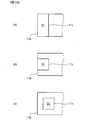
上記実施形態において、フィルタ収納部31は、筐体11のコーナー部に形成され、L字形状の第1の隔壁11cによりフィルタ回路部130と仕切られている構造として例示した。しかし、図19(a)に示すように、フィルタ収納部31は、周側壁11bを、平面視でコ字形状に形成し、コ字形状の開口部に、この開口部を塞ぐように第1の隔壁11cを形成する構造とすることもできる。この構造の場合には、第1の隔壁11cは、直線状となり、電磁ノイズ伝播低減構造も、第1の隔壁11cに沿う直線状に形成すればよい。
逆に、図19(b)に示すように、第1の隔壁11cを平面視でコ字形状に形成し、このコ字形状の開口部を、筐体11の側壁で塞ぐ構造とすることもできる。この構造では、電磁ノイズ伝播低減構造は、第1の隔壁11cに沿って、コ字形状に形成することが望ましい。
さらに、図19(c)に示すように、第1の隔壁11cを、筐体11の周側壁11bの内部に、枠状に形成することもできる。この構造では、電磁ノイズ伝播低減構造は、第1の隔壁11cに沿って枠状に形成することが望ましい。
逆に、図19(b)に示すように、第1の隔壁11cを平面視でコ字形状に形成し、このコ字形状の開口部を、筐体11の側壁で塞ぐ構造とすることもできる。この構造では、電磁ノイズ伝播低減構造は、第1の隔壁11cに沿って、コ字形状に形成することが望ましい。
さらに、図19(c)に示すように、第1の隔壁11cを、筐体11の周側壁11bの内部に、枠状に形成することもできる。この構造では、電磁ノイズ伝播低減構造は、第1の隔壁11cに沿って枠状に形成することが望ましい。
制御回路基板151に形成された制御回路部の接地パターンは、ベース板12に締結部材152に固定されて同電位とされている構造として例示した。しかし、制御回路部の接地パターンは、コンデンサを介してベース板12に接続するようにしてもよい。
上記実施形態では、ノイズを放射する能動回路として、DC-DCコンバータ100およびインバータ200を例示した。しかし、本発明は、これに限らず、他の電力変換装置に対しても適用が可能である。
以上の説明は一例であり、本発明は上記実施形態に限定されない。
要は、金属など導電性を有する材料で形成された筐体内に、ノイズを放射する能動回路部と、出力側のフィルタ回路部とが形成された電力変換装置において、能動回路部とフィルタ回路部との間に配置された第1の隔壁を有する筐体と、第1の隔壁とフィルタ回路部の間に配置された第2の隔壁を有するベース板とを備えるものであればよい。筐体やベース板は導電性を持つ素材から形成されればよく、金属製に限定されない。
要は、金属など導電性を有する材料で形成された筐体内に、ノイズを放射する能動回路部と、出力側のフィルタ回路部とが形成された電力変換装置において、能動回路部とフィルタ回路部との間に配置された第1の隔壁を有する筐体と、第1の隔壁とフィルタ回路部の間に配置された第2の隔壁を有するベース板とを備えるものであればよい。筐体やベース板は導電性を持つ素材から形成されればよく、金属製に限定されない。
次の優先権基礎出願の開示内容は引用文としてここに組み込まれる。
日本国特許出願2015年第35485号(2015年2月25日出願)
日本国特許出願2015年第35485号(2015年2月25日出願)
11 筐体
11b 周側壁
11c 第1の隔壁
11d 第5の隔壁
12 ベース板
12b 第2の隔壁
12c 第3の隔壁
12d 第4の隔壁
14 ケース蓋
16 凹部
17 隙間
31 フィルタ収納部
32 変換用回路部収納部
50、50A~50E 電磁ノイズ伝播低減構造
61 上面
61a 取付部(締結用突部)
71 仕切り壁
72 側壁
100 電力変換装置(DCDCコンバータ)
100A 電力変換装置
110 高電圧スイッチング回路部
120 低電圧スイッチング回路部(能動回路部)
130、140 フィルタ回路部
151 制御回路基板
200 インバータ回路(能動回路部)
11b 周側壁
11c 第1の隔壁
11d 第5の隔壁
12 ベース板
12b 第2の隔壁
12c 第3の隔壁
12d 第4の隔壁
14 ケース蓋
16 凹部
17 隙間
31 フィルタ収納部
32 変換用回路部収納部
50、50A~50E 電磁ノイズ伝播低減構造
61 上面
61a 取付部(締結用突部)
71 仕切り壁
72 側壁
100 電力変換装置(DCDCコンバータ)
100A 電力変換装置
110 高電圧スイッチング回路部
120 低電圧スイッチング回路部(能動回路部)
130、140 フィルタ回路部
151 制御回路基板
200 インバータ回路(能動回路部)
Claims (11)
- ノイズを放射する能動回路部と、
出力側のフィルタ回路部と、
前記能動回路部と前記フィルタ回路部とをそれぞれ収納する第1の空間および第2の空間を有する筐体と、
少なくとも前記第1の空間を覆うように設けられ、前記筐体と電気的に接続されるベース板とを備え、
前記筐体は、前記第1の空間と前記第2の空間とを区画する第1の隔壁を有し、
前記ベース板は、前記第1の空間を覆って配置され、かつ、前記第1の隔壁に沿う第2の隔壁を有し、
前記第2の隔壁は、前記第1の空間内において前記フィルタ回路部と前記第1の隔壁との間に配置されている、電力変換装置。 - 請求項1に記載の電力変換装置において、
前記第1の隔壁は、前記筐体に一体成形されており、
前記第2の隔壁は、前記ベース板に一体成形されている、電力変換装置。 - 請求項2に記載の電力変換装置において、
前記ベース板は、前記第1の隔壁の上面に締結部材により締結されている、電力変換装置。 - 請求項3に記載の電力変換装置において、
前記第1の隔壁の前記上面には、前記ベース板が面接触で締結される締結用突部が形成されている、電力変換装置。 - 請求項1に記載の電力変換装置において、
前記ベース板は、前記第1の隔壁よりも前記能動回路部側に、前記第1の隔壁に沿う第3の隔壁を有する、電力変換装置。 - 請求項1に記載の電力変換装置において、
前記筐体は、前記フィルタ回路部の周囲に設けられた側壁を有し、
前記ベース板は、前記第1の空間において前記側壁の内面に沿って形成された第4の隔壁を有する、電力変換装置。 - 請求項6に記載の電力変換装置において、
前記第4の隔壁は、前記ベース板に一体成形されている、電力変換装置。 - 請求項1から請求項4、請求項6、請求項7のいずれか1項に記載の電力変換装置において、
前記筐体は、前記第2の隔壁よりも前記フィルタ回路部側に、前記第1の隔壁に沿う第5の隔壁を有する、電力変換装置。 - DC-DCコンバータ回路と、
前記DC-DCコンバータ回路に接続された出力側のフィルタ回路部と、
インバータ回路と、
前記DC-DCコンバータ回路と、前記フィルタ回路部と、前記インバータ回路とを収納する金属製の筐体と、
前記金属製の筐体と電気的に接続される金属製のベース板とを備え、
前記筐体は、前記DC-DCコンバータ回路および前記インバータ回路から前記フィルタ回路部をシールドする第1の筐体側隔壁および前記フィルタ回路部の周囲に配置された側壁を有し、
前記筐体は、前記第1の筐体側隔壁と前記筐体の前記側壁とで区画され、前記フィルタ回路部が収納される第1の空間を有し、
前記ベース板は、前記第1の空間を覆って配置され、かつ、前記側壁の内面に沿って形成され、前記フィルタ回路部側に延出された第1のベース板側隔壁を有する、電力変換装置。 - 請求項9に記載の電力変換装置において、
前記ベース板は、さらに、前記第1の筐体側隔壁と前記DC-DCコンバータ回路との間に配置された第2のベース板側隔壁を有する、電力変換装置。 - 請求項10に記載の電力変換装置において、
前記筐体は、さらに、前記第1の筐体側隔壁と前記フィルタ回路部との間に配置された第2の筐体側隔壁を有する、電力変換装置。
Priority Applications (3)
| Application Number | Priority Date | Filing Date | Title |
|---|---|---|---|
| CN201580069194.3A CN107112902B (zh) | 2015-02-25 | 2015-12-25 | 电力变换装置 |
| US15/545,762 US10103619B2 (en) | 2015-02-25 | 2015-12-25 | Electric power conversion device |
| DE112015005695.5T DE112015005695T5 (de) | 2015-02-25 | 2015-12-25 | Vorrichtung zum Umsetzen elektrischer Leistung |
Applications Claiming Priority (2)
| Application Number | Priority Date | Filing Date | Title |
|---|---|---|---|
| JP2015035485A JP6218150B2 (ja) | 2015-02-25 | 2015-02-25 | 電力変換装置 |
| JP2015-035485 | 2015-02-25 |
Publications (1)
| Publication Number | Publication Date |
|---|---|
| WO2016136115A1 true WO2016136115A1 (ja) | 2016-09-01 |
Family
ID=56788199
Family Applications (1)
| Application Number | Title | Priority Date | Filing Date |
|---|---|---|---|
| PCT/JP2015/086234 Ceased WO2016136115A1 (ja) | 2015-02-25 | 2015-12-25 | 電力変換装置 |
Country Status (5)
| Country | Link |
|---|---|
| US (1) | US10103619B2 (ja) |
| JP (1) | JP6218150B2 (ja) |
| CN (1) | CN107112902B (ja) |
| DE (1) | DE112015005695T5 (ja) |
| WO (1) | WO2016136115A1 (ja) |
Families Citing this family (10)
| Publication number | Priority date | Publication date | Assignee | Title |
|---|---|---|---|---|
| CN108123617B (zh) * | 2016-11-29 | 2020-05-05 | 台达电子企业管理(上海)有限公司 | 用于安装高低压转换电路的装置、高低压转换系统及电源 |
| JP7052609B2 (ja) * | 2018-07-11 | 2022-04-12 | 株式会社デンソー | 電力変換装置 |
| DE102018129415B4 (de) * | 2018-11-22 | 2024-07-04 | Dr. Ing. H.C. F. Porsche Aktiengesellschaft | Ladevorrichtung für ein Fahrzeug und Fahrzeug mit einer Ladevorrichtung |
| CN113615227A (zh) | 2019-01-10 | 2021-11-05 | Mhm微技术责任有限公司 | 可连接网络的感测装置 |
| CN113826315B (zh) * | 2019-05-13 | 2025-01-03 | 日立安斯泰莫株式会社 | 电力转换装置 |
| US12119756B2 (en) * | 2020-04-20 | 2024-10-15 | Hitachi Industrial Equipment Systems Co., Ltd. | Power conversion device |
| JP7515588B2 (ja) | 2020-07-03 | 2024-07-12 | 三菱電機株式会社 | 電力変換装置 |
| JP7322835B2 (ja) * | 2020-08-21 | 2023-08-08 | 株式会社デンソー | 電力変換装置 |
| JP7563487B2 (ja) * | 2020-12-21 | 2024-10-08 | 株式会社村田製作所 | スイッチング電源装置 |
| WO2023276797A1 (ja) * | 2021-06-28 | 2023-01-05 | 株式会社村田製作所 | スイッチング電源装置 |
Citations (4)
| Publication number | Priority date | Publication date | Assignee | Title |
|---|---|---|---|---|
| JPS6045479U (ja) * | 1983-09-05 | 1985-03-30 | 松下電器産業株式会社 | 電子機器筐体 |
| JPH11299260A (ja) * | 1998-04-15 | 1999-10-29 | Matsushita Electric Works Ltd | 電源装置 |
| JP2013090533A (ja) * | 2011-10-21 | 2013-05-13 | Denso Corp | 電源装置 |
| JP2013099057A (ja) * | 2011-10-31 | 2013-05-20 | Hitachi Automotive Systems Ltd | 電子装置 |
Family Cites Families (8)
| Publication number | Priority date | Publication date | Assignee | Title |
|---|---|---|---|---|
| JPS62162891U (ja) * | 1986-04-03 | 1987-10-16 | ||
| US4717990A (en) * | 1986-05-30 | 1988-01-05 | Motorola, Inc. | Double-shielded housing for RF circuitry |
| DE10019696B4 (de) * | 1999-04-22 | 2007-06-06 | International Rectifier Corp., El Segundo | Schaltung zur Verringerung von Störstrahlung in Motorspeiseschaltungsanwendungen |
| JP3961812B2 (ja) * | 2001-10-31 | 2007-08-22 | 富士通株式会社 | 電源装置及びその制御方法 |
| US6965514B2 (en) * | 2002-01-16 | 2005-11-15 | Rockwell Automation Technologies, Inc. | Fluid cooled vehicle drive module |
| CN103262400A (zh) * | 2010-08-18 | 2013-08-21 | 芬斯克斯有限公司 | 基于电池的甚高频开关功率变换器 |
| EP2787627B1 (en) * | 2011-11-28 | 2022-12-07 | Nissan Motor Co., Ltd. | Power conversion device |
| JP5789576B2 (ja) * | 2012-09-14 | 2015-10-07 | 日立オートモティブシステムズ株式会社 | 電力変換装置 |
-
2015
- 2015-02-25 JP JP2015035485A patent/JP6218150B2/ja active Active
- 2015-12-25 US US15/545,762 patent/US10103619B2/en active Active
- 2015-12-25 CN CN201580069194.3A patent/CN107112902B/zh active Active
- 2015-12-25 DE DE112015005695.5T patent/DE112015005695T5/de active Pending
- 2015-12-25 WO PCT/JP2015/086234 patent/WO2016136115A1/ja not_active Ceased
Patent Citations (4)
| Publication number | Priority date | Publication date | Assignee | Title |
|---|---|---|---|---|
| JPS6045479U (ja) * | 1983-09-05 | 1985-03-30 | 松下電器産業株式会社 | 電子機器筐体 |
| JPH11299260A (ja) * | 1998-04-15 | 1999-10-29 | Matsushita Electric Works Ltd | 電源装置 |
| JP2013090533A (ja) * | 2011-10-21 | 2013-05-13 | Denso Corp | 電源装置 |
| JP2013099057A (ja) * | 2011-10-31 | 2013-05-20 | Hitachi Automotive Systems Ltd | 電子装置 |
Also Published As
| Publication number | Publication date |
|---|---|
| JP6218150B2 (ja) | 2017-10-25 |
| CN107112902A (zh) | 2017-08-29 |
| DE112015005695T5 (de) | 2017-09-07 |
| JP2016158423A (ja) | 2016-09-01 |
| US20180019663A1 (en) | 2018-01-18 |
| US10103619B2 (en) | 2018-10-16 |
| CN107112902B (zh) | 2019-09-10 |
Similar Documents
| Publication | Publication Date | Title |
|---|---|---|
| JP6218150B2 (ja) | 電力変換装置 | |
| JP5743851B2 (ja) | 電子装置 | |
| JP6175556B2 (ja) | 電力変換装置 | |
| JP6101484B2 (ja) | Dc−dcコンバータ | |
| US10128770B2 (en) | Converter and electric power conversion apparatus | |
| JP6897671B2 (ja) | 車載用の電力変換装置 | |
| JP6104347B1 (ja) | 電力変換装置 | |
| US9425695B2 (en) | DC-DC converter | |
| WO2014033852A1 (ja) | 車載用電力変換装置 | |
| EP3057216B1 (en) | Dc-dc converter device | |
| JP6486443B1 (ja) | 電力変換装置 | |
| JP6719021B2 (ja) | 電力変換装置 | |
| KR20080094828A (ko) | 캐패시터 장치 | |
| JP4396627B2 (ja) | 電力変換装置 | |
| US20170222570A1 (en) | Power Conversion Device | |
| JP2008054384A (ja) | 電力変換装置 | |
| JP5941773B2 (ja) | Dc−dcコンバータ | |
| JP6851999B2 (ja) | 電力変換装置 | |
| CN111313656B (zh) | 电源装置 |
Legal Events
| Date | Code | Title | Description |
|---|---|---|---|
| 121 | Ep: the epo has been informed by wipo that ep was designated in this application |
Ref document number: 15883405 Country of ref document: EP Kind code of ref document: A1 |
|
| WWE | Wipo information: entry into national phase |
Ref document number: 112015005695 Country of ref document: DE |
|
| WWE | Wipo information: entry into national phase |
Ref document number: 15545762 Country of ref document: US |
|
| 122 | Ep: pct application non-entry in european phase |
Ref document number: 15883405 Country of ref document: EP Kind code of ref document: A1 |