WO2016132847A1 - Cu合金膜およびCu積層膜 - Google Patents
Cu合金膜およびCu積層膜 Download PDFInfo
- Publication number
- WO2016132847A1 WO2016132847A1 PCT/JP2016/052499 JP2016052499W WO2016132847A1 WO 2016132847 A1 WO2016132847 A1 WO 2016132847A1 JP 2016052499 W JP2016052499 W JP 2016052499W WO 2016132847 A1 WO2016132847 A1 WO 2016132847A1
- Authority
- WO
- WIPO (PCT)
- Prior art keywords
- film
- layer
- atomic
- alloy
- less
- Prior art date
- Legal status (The legal status is an assumption and is not a legal conclusion. Google has not performed a legal analysis and makes no representation as to the accuracy of the status listed.)
- Ceased
Links
Images


Classifications
-
- C—CHEMISTRY; METALLURGY
- C22—METALLURGY; FERROUS OR NON-FERROUS ALLOYS; TREATMENT OF ALLOYS OR NON-FERROUS METALS
- C22C—ALLOYS
- C22C9/00—Alloys based on copper
-
- C—CHEMISTRY; METALLURGY
- C22—METALLURGY; FERROUS OR NON-FERROUS ALLOYS; TREATMENT OF ALLOYS OR NON-FERROUS METALS
- C22C—ALLOYS
- C22C9/00—Alloys based on copper
- C22C9/01—Alloys based on copper with aluminium as the next major constituent
-
- C—CHEMISTRY; METALLURGY
- C22—METALLURGY; FERROUS OR NON-FERROUS ALLOYS; TREATMENT OF ALLOYS OR NON-FERROUS METALS
- C22C—ALLOYS
- C22C9/00—Alloys based on copper
- C22C9/02—Alloys based on copper with tin as the next major constituent
-
- C—CHEMISTRY; METALLURGY
- C22—METALLURGY; FERROUS OR NON-FERROUS ALLOYS; TREATMENT OF ALLOYS OR NON-FERROUS METALS
- C22C—ALLOYS
- C22C9/00—Alloys based on copper
- C22C9/04—Alloys based on copper with zinc as the next major constituent
-
- C—CHEMISTRY; METALLURGY
- C22—METALLURGY; FERROUS OR NON-FERROUS ALLOYS; TREATMENT OF ALLOYS OR NON-FERROUS METALS
- C22C—ALLOYS
- C22C9/00—Alloys based on copper
- C22C9/05—Alloys based on copper with manganese as the next major constituent
-
- C—CHEMISTRY; METALLURGY
- C22—METALLURGY; FERROUS OR NON-FERROUS ALLOYS; TREATMENT OF ALLOYS OR NON-FERROUS METALS
- C22C—ALLOYS
- C22C9/00—Alloys based on copper
- C22C9/06—Alloys based on copper with nickel or cobalt as the next major constituent
-
- C—CHEMISTRY; METALLURGY
- C23—COATING METALLIC MATERIAL; COATING MATERIAL WITH METALLIC MATERIAL; CHEMICAL SURFACE TREATMENT; DIFFUSION TREATMENT OF METALLIC MATERIAL; COATING BY VACUUM EVAPORATION, BY SPUTTERING, BY ION IMPLANTATION OR BY CHEMICAL VAPOUR DEPOSITION, IN GENERAL; INHIBITING CORROSION OF METALLIC MATERIAL OR INCRUSTATION IN GENERAL
- C23C—COATING METALLIC MATERIAL; COATING MATERIAL WITH METALLIC MATERIAL; SURFACE TREATMENT OF METALLIC MATERIAL BY DIFFUSION INTO THE SURFACE, BY CHEMICAL CONVERSION OR SUBSTITUTION; COATING BY VACUUM EVAPORATION, BY SPUTTERING, BY ION IMPLANTATION OR BY CHEMICAL VAPOUR DEPOSITION, IN GENERAL
- C23C14/00—Coating by vacuum evaporation, by sputtering or by ion implantation of the coating forming material
- C23C14/06—Coating by vacuum evaporation, by sputtering or by ion implantation of the coating forming material characterised by the coating material
- C23C14/14—Metallic material, boron or silicon
-
- C—CHEMISTRY; METALLURGY
- C23—COATING METALLIC MATERIAL; COATING MATERIAL WITH METALLIC MATERIAL; CHEMICAL SURFACE TREATMENT; DIFFUSION TREATMENT OF METALLIC MATERIAL; COATING BY VACUUM EVAPORATION, BY SPUTTERING, BY ION IMPLANTATION OR BY CHEMICAL VAPOUR DEPOSITION, IN GENERAL; INHIBITING CORROSION OF METALLIC MATERIAL OR INCRUSTATION IN GENERAL
- C23C—COATING METALLIC MATERIAL; COATING MATERIAL WITH METALLIC MATERIAL; SURFACE TREATMENT OF METALLIC MATERIAL BY DIFFUSION INTO THE SURFACE, BY CHEMICAL CONVERSION OR SUBSTITUTION; COATING BY VACUUM EVAPORATION, BY SPUTTERING, BY ION IMPLANTATION OR BY CHEMICAL VAPOUR DEPOSITION, IN GENERAL
- C23C14/00—Coating by vacuum evaporation, by sputtering or by ion implantation of the coating forming material
- C23C14/22—Coating by vacuum evaporation, by sputtering or by ion implantation of the coating forming material characterised by the process of coating
- C23C14/34—Sputtering
-
- H—ELECTRICITY
- H01—ELECTRIC ELEMENTS
- H01B—CABLES; CONDUCTORS; INSULATORS; SELECTION OF MATERIALS FOR THEIR CONDUCTIVE, INSULATING OR DIELECTRIC PROPERTIES
- H01B1/00—Conductors or conductive bodies characterised by the conductive materials; Selection of materials as conductors
- H01B1/02—Conductors or conductive bodies characterised by the conductive materials; Selection of materials as conductors mainly consisting of metals or alloys
-
- H—ELECTRICITY
- H10—SEMICONDUCTOR DEVICES; ELECTRIC SOLID-STATE DEVICES NOT OTHERWISE PROVIDED FOR
- H10P—GENERIC PROCESSES OR APPARATUS FOR THE MANUFACTURE OR TREATMENT OF DEVICES COVERED BY CLASS H10
- H10P14/00—Formation of materials, e.g. in the shape of layers or pillars
- H10P14/40—Formation of materials, e.g. in the shape of layers or pillars of conductive or resistive materials
-
- H—ELECTRICITY
- H10—SEMICONDUCTOR DEVICES; ELECTRIC SOLID-STATE DEVICES NOT OTHERWISE PROVIDED FOR
- H10W—GENERIC PACKAGES, INTERCONNECTIONS, CONNECTORS OR OTHER CONSTRUCTIONAL DETAILS OF DEVICES COVERED BY CLASS H10
- H10W20/00—Interconnections in chips, wafers or substrates
- H10W20/01—Manufacture or treatment
-
- H—ELECTRICITY
- H10—SEMICONDUCTOR DEVICES; ELECTRIC SOLID-STATE DEVICES NOT OTHERWISE PROVIDED FOR
- H10W—GENERIC PACKAGES, INTERCONNECTIONS, CONNECTORS OR OTHER CONSTRUCTIONAL DETAILS OF DEVICES COVERED BY CLASS H10
- H10W20/00—Interconnections in chips, wafers or substrates
- H10W20/40—Interconnections external to wafers or substrates, e.g. back-end-of-line [BEOL] metallisations or vias connecting to gate electrodes
- H10W20/45—Interconnections external to wafers or substrates, e.g. back-end-of-line [BEOL] metallisations or vias connecting to gate electrodes characterised by their insulating parts
- H10W20/48—Insulating materials thereof
Definitions
- the present invention relates to a Cu alloy film and a Cu laminated film.
- ITO thin films and Al thin films have been used for flat panel displays such as liquid crystal panels and organic EL panels, and wiring for touch panels.
- a wiring having a lower electric resistance than before is required, and a wiring electrode using a film made of pure Cu or a Cu-based alloy has been proposed.
- Cu has a high affinity with oxygen, it is oxidized by heating in the presence of oxygen and the passage of time, leading to discoloration and an increase in electrical resistance.
- Patent Document 1 proposes a sputtering target used when forming a protective film on one or both surfaces of a Cu wiring film.
- the sputtering target is 8.0% by mass or more and 11.0% by mass or less of Al, 3.0% by mass or more and 5.0% by mass or less of Fe, and 0.5% by mass or more and 2.0% by mass of Ni.
- Mn is contained in an amount of 0.5% by mass or more and 2.0% by mass or less, with the balance being Cu and inevitable impurities.
- Patent Document 1 shows that the film formed by the sputtering target becomes a protective film that suppresses discoloration during a weather resistance test that is exposed for 250 hours at a temperature of 60 ° C. and a relative humidity of 90%. .
- Patent Document 2 includes 20.0 to 40.0% by mass of nickel as a Cu alloy sputtering target, and any one of Cr, Ti, V, Al, Ta, Co, Zr, Nb, and Mo or these
- a Cu alloy sputtering target characterized in that two or more elements are added in a total amount of 1.0 to 10.0% by mass, and the balance is copper and inevitable impurities.
- the metal thin film formed using this Cu alloy sputtering target is excellent in oxidation resistance and corrosion resistance compared with Cu etc., and is used as a wiring material and a protective film of a wiring material.
- Patent Document 3 a wiring structure including a semiconductor layer of a thin film transistor, a Cu alloy film used for an electrode, and a protective film in order from the substrate side on the substrate, wherein the semiconductor layer is made of an oxide semiconductor,
- the Cu alloy film has a laminated structure including a first layer (X) and a second layer (Z) in order from the substrate side, and in particular, the second layer (Z) includes Zn, Ni, Ti, Al, Proposing a wiring structure made of a Cu—Z alloy containing a total of 2 to 20 atomic% of at least one Z group element selected from the group consisting of Mg, Ca, W, Nb, rare earth elements, Ge, and Mn Yes.
- the wiring film includes at least one alloy element selected from the group consisting of Ni, Zn, and Mn.
- JP 2014-156621 A Japanese Patent Application Laid-Open No. 2013-133489 Japanese Unexamined Patent Publication No. 2012-243779 JP 2013-120411 A
- the present invention has been made in view of the above problems, and its object is to provide a Cu alloy film that exhibits low electrical resistance and excellent oxidation resistance, and that can be satisfactorily processed by a wet etching method. It is to propose a Cu laminated film including the Cu alloy film, a laminated body having the Cu laminated film, and a sputtering target for forming the Cu alloy film.
- excellent wet etching processability the fact that the wiring process can be satisfactorily performed by the wet etching method is sometimes referred to as “excellent wet etching processability”.
- the Cu alloy film of the present invention capable of solving the above-described problems contains Ni in an amount of 3.0 atomic% or more and 19.0 atomic% or less, and is one kind of X selected from the group consisting of Al, Zn, Mn, and Sn.
- the element is contained, the remainder is made of Cu and inevitable impurities, and the content of the X element is not less than x atomic% obtained from the following formula (1), and the X element is Zn or Mn
- the total amount of Ni and X elements is 20.0 atomic% or more.
- the X element is Al or Sn
- the total amount of Ni and X elements is 16.0 atomic% or more. .
- the Cu alloy film is referred to as a “Cu—Ni—X film”, and a film made of a Cu-based alloy in the first layer described later may be referred to as a “Cu-based alloy film”.
- x 1.96 ⁇ Ni + 1.64 (1)
- Ni indicates the Ni content in atomic% in the Cu alloy film.
- the Cu laminated film of the present invention that has solved the above-mentioned problems is characterized by having a film made of pure Cu or a Cu-based alloy as a first layer and the Cu—Ni—X film as a second layer.
- the film thickness of the second layer is 10 nm or more and 200 nm or less.
- the Cu-based alloy in the first layer contains at least one Z element selected from the group consisting of Ti, Mn, Fe, Co, Ni, Ge, and Zn, with the balance being It consists of Cu and inevitable impurities.
- the present invention may include a laminate having the Cu laminated film on a substrate. Further, the present invention can include a wiring electrode, an input device, and a touch panel sensor using the Cu laminated film or the laminated body. Further, the present invention may include a Cu alloy sputtering target for forming the Cu—Ni—X film.
- a Cu—Ni—X film having low electrical resistance and excellent oxidation resistance and wet etching processability; and oxidation resistance comprising the Cu—Ni—X film as an oxidation resistant protective film, for example.
- a Cu laminated film excellent in wet etching processability; a laminated body having the Cu laminated film; and a wiring electrode using the laminated body for example.
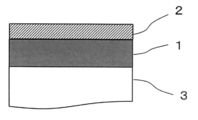
- FIG. 1 is a schematic cross-sectional view illustrating the configuration of the laminate of the invention.
- FIG. 2 is a schematic cross-sectional view illustrating another configuration of the laminate of the invention.
- FIG. 3 is a schematic cross-sectional view illustrating another configuration of the laminate of the invention.
- the inventors of the present invention have made extensive studies to solve the above-mentioned problems.
- the inventors In order to obtain a Cu alloy film based on Cu exhibiting a low electrical resistance and excellent in oxidation resistance and excellent in wet etching processability, the inventors have intensively studied particularly alloy elements.
- Ni diffuses in the film, concentrates on the surface, and is further oxidized to form oxidized Ni, which is passivated to protect the surface of the Cu—Ni—X film and contribute to the improvement of oxidation resistance.
- Ni content When the Ni content is less than 3.0 atomic%, sufficient oxidation resistance cannot be ensured even when the element X described later is included. Therefore, in this invention, Ni content shall be 3.0 atomic% or more.
- the Ni content may be simply referred to as Ni amount.
- the amount of Ni is preferably 4 atomic% or more, more preferably 5.0 atomic% or more, and further preferably 6.0 atomic% or more.
- the Ni content is 19.0 atomic% or less.
- the amount of Ni is preferably 12 atomic percent or less, more preferably 10 atomic percent or less.
- the elements X, Al, Zn, Mn and Sn are diffused in the film, concentrated on the surface and further oxidized to form oxide X and passivate to protect the surface of the Cu—Ni—X film. Contributes to the improvement of oxidation resistance. Further, these elements are more easily dissolved in an etching solution such as an iron chloride-containing etching solution than Ni, and contribute to improvement of wet etching processability.
- Zn and Sn are elements with low vapor pressure. Therefore, when a Cu—Ni—X film is formed by a sputtering method, a composition shift or the like is more likely to occur than Al or Mn. Therefore, from the viewpoint of ease of use, it is preferable to use Al or Mn as the X element.
- the upper limit of the content of the X element is not particularly limited.
- a preferable method for producing the Cu—Ni—X film is a sputtering method. From the viewpoint of ease of production of a sputtering target used in this sputtering method, the content of the element X should be 50 atomic% or less. Is preferable, more preferably 40 atomic percent or less, and still more preferably 30 atomic percent or less.
- the upper limit of the content is preferably 50 atomic% or less. This is because if the Al amount exceeds 50 atomic%, a residue derived from Al oxide is likely to be generated during wiring processing, that is, wet etching processability is likely to deteriorate.
- the upper limit of the Al content is more preferably 40 atomic% or less, and still more preferably 30 atomic% or less.
- the lower limit value of the total amount of Ni and X element is also defined according to the type of X element.
- the total amount of Ni and X element is used to suppress an increase in eave width during wiring processing by a reflectance change amount and a wet etching method before and after heat treatment, and excellent oxidation resistance and From the viewpoint of ensuring wet etching processability, the content is made 20.0 atomic% or more.
- the total amount is preferably 25.0 atomic% or more.
- the total amount is preferably 40.0 atomic% or less from the viewpoint of ease of production of the sputtering target used for forming the thin film.
- the total amount of Ni and X elements is reduced in the reflectance change before and after the heat treatment and the increase in the eave width during wiring processing by the wet etching method, and has excellent oxidation resistance. And from the viewpoint of securing wet etching processability, it is set to 16.0 atomic% or more.
- the total amount is preferably 20.0 atomic% or more, more preferably 25.0 atomic% or more.
- the total amount is preferably 45.0 atomic% or less, more preferably 43.0 atomic% or less, and still more preferably 40.0 atoms. % Or less.
- the Cu—Ni—X film contains 3.0 atomic% or more and 19.0 atomic% or less of Ni, and contains one kind of X element selected from the group consisting of Al, Zn, Mn, and Sn as described above. It is included so that the total amount with Ni is equal to or more than the lower limit according to the amount of Ni, and the remaining amount is made of Cu and inevitable impurities.
- the film thickness of the Cu—Ni—X film is not particularly limited. For example, it can be 10 nm or more and 200 nm or less. When forming a Cu laminated film including the Cu—Ni—X film, it is recommended that the film thickness of the Cu—Ni—X film be as described below.
- the present invention also includes a Cu laminated film obtained by laminating a film made of pure Cu or a Cu-based alloy as the first layer and the Cu—Ni—X film as the second layer.
- the first layer may be formed as a conductive layer
- the second layer of Cu—Ni—X film may be formed as an oxidation-resistant protective film of the first layer.
- a film made of pure Cu or a Cu-based alloy is used as the first layer.
- this “film made of pure Cu or a Cu-based alloy” may be referred to as “Cu-based film”.
- the first layer is a Cu-based film and preferably has an electric resistivity of 10 ⁇ ⁇ cm or less, more preferably 5 ⁇ ⁇ cm or less.
- the first layer Cu-based alloy film there is a film containing at least one Z element selected from the group consisting of Ti, Mn, Fe, Co, Ni, Ge, and Zn, with the balance being Cu and inevitable impurities. Can be mentioned. By including the Z element, there are effects such as improvement of various corrosion resistances and adhesion to the substrate.
- the oxidation resistance and wet etching processability desired in the present invention can be achieved by forming the prescribed second layer, and does not depend on the composition of the first layer.
- the Z element may be contained in a total amount exceeding 0 atomic% and not exceeding 2 atomic%.
- the film thickness of the second layer is preferably 10 nm or more, more preferably 30 nm or more in order to ensure sufficient oxidation resistance.
- the film thickness of the second layer is preferably 200 nm or less, and more preferably 100 nm or less.
- the film thickness of the first layer is preferably 20 nm or more, more preferably 50 nm or more from the viewpoint of obtaining a film having a uniform film thickness and components during film formation.
- the thickness of the first layer is preferably 500 nm or less, and more preferably 400 nm or less.
- the total film thickness of the first layer and the second layer is preferably 30 nm or more, and more preferably 50 nm or more.
- the total film thickness is preferably 600 nm or less, more preferably 500 nm or less, and still more preferably 400 nm or less.
- the present invention includes a Cu laminate film, that is, a laminate having the first layer and the second layer on a substrate.
- the laminate may include other layers such as an adhesion layer.
- adhesion layer the form of this laminate will be described with reference to patterns.
- FIG. 1 is a schematic cross-sectional view illustrating the configuration of the laminate of the present invention.
- a film made of pure Cu or a Cu-based alloy as the first layer 1 is provided on the substrate 3, and a Cu—Ni—X film as the second layer 2 is provided on the upper surface thereof.
- Two layers 2 protect the first layer 1.
- the substrate 3 include a glass substrate, a film substrate, a plastic substrate, a quartz substrate, and a silicon substrate.
- FIGS. 2 and 3 are schematic cross-sectional views showing a modification of the laminate shown in FIG.
- the substrate 3, the first layer 1, and the second layer 2 in FIGS. 2 and 3 are the same as those in FIG. 1.
- the second layer 2 protects the first layer 1, that is, the second layer 2 is the most. It has a structure that is a surface layer.
- FIG. 2 shows a structure in which the adhesion layer 4 is provided between the substrate 3 and the first layer 1 in FIG.
- the adhesion layer 4 is not particularly limited as long as it is generally used, and examples thereof include a Ti film, a Mo film, a Ni film, a Cr film, and the like having a film thickness of 5 to 30 nm.
- FIG. 3 shows a structure in which the adhesion layer 4 is provided between the substrate 3 and the first layer 1 and between the first layer 1 and the second layer 2 in FIG.
- the adhesion layer 4 in FIG. 3 may be any one that is generally used, for example, a Ti film, a Mo film, a Ni film, a Cr film, and the like having a film thickness of 5 to 30 nm, for example. .
- the Cu—Ni—X film is preferably formed by a sputtering method. If the sputtering method is used, a Cu—Ni—X film having almost the same composition as the sputtering target can be formed.
- a sputtering method for example, any sputtering method such as a DC sputtering method, an RF sputtering method, a magnetron sputtering method, or a reactive sputtering method may be employed, and the formation conditions may be set as appropriate.
- the target is made of a Cu alloy containing a predetermined amount of the Ni or X element, and the desired Cu—Ni— film is formed.
- a Cu alloy sputtering target having the same composition as that of the X film is used, a Cu—Ni—X film having a desired component and composition can be formed without causing a composition shift.
- two or more pure metal targets or alloy targets having different compositions may be used, and these may be discharged simultaneously to form a film. Or you may form into a film, adjusting a component by carrying out chip-on of the metal of an alloy element to a pure Cu target.
- sputtering conditions Film forming method: Sputtering method Film forming apparatus: CS-200 manufactured by ULVAC Substrate temperature: room temperature Deposition gas: Ar gas Gas pressure: 2 mTorr Sputtering power: 10 to 500W Degree of vacuum: 1 ⁇ 10 -6 Torr or less
- the Cu alloy sputtering target of the present invention may have any shape depending on the shape and structure of the sputtering apparatus, such as a square plate shape, a circular plate shape, and a donut plate shape.
- a method for producing the Cu alloy sputtering target a method in which an ingot made of a Cu-based alloy is produced by a melt casting method or a powder sintering method; a preform made of a Cu-based alloy, that is, a final dense body is obtained. Examples thereof include a spray forming method in which the preform is produced by densifying the preform with a densification means after the previous intermediate is produced.
- each layer other than the Cu—Ni—X film As a method for forming each layer other than the Cu—Ni—X film, a method usually used in the technical field of the present invention can be appropriately employed.
- the laminate having the Cu—Ni—X film can be applied to wiring electrodes and input devices.
- the input device includes an input device having an input unit in a display device such as a touch panel, and an input device having no display device such as a touch pad.
- the Cu—Ni—X film of the present invention is preferably used for a touch panel sensor.
- an etchant containing iron chloride is used as an etchant used for wet etching, but the present invention is not limited to this.
- An etchant containing ammonium persulfate, an etchant containing hydrogen peroxide, phosphoric acid, A mixed acid etching solution containing nitric acid and acetic acid can also be used.
- Laminate Sample As a transparent substrate, an alkali-free glass plate having a diameter of 4 inches and a thickness of 0.7 mm was prepared, and on this alkali-free glass plate, a DC magnetron sputtering method was used. A Cu laminated film of the first layer and the second layer shown in 4 was formed. Specifically, in Table 2, a Cu laminated film including a pure Cu film as the first layer and a Cu—Ni—X film as the second layer was formed. In Table 3, various Cu-based alloy films were formed as the first layer, and a Cu—Ni—Al film containing Ni 6.4 atomic% and Al 29.3 atomic% was formed as the second layer.
- a pure Cu film is formed as the first layer
- a Cu—Ni—Al film containing Ni 6.4 atomic% and Al 29.3 atomic% is formed as the second layer
- the films of the first layer and the second layer are formed.
- the thickness was changed.
- a sample in which only the Cu-based film described in Table 1 was formed on the non-alkali glass plate was also prepared.
- the atmosphere in the chamber is once adjusted to an ultimate vacuum of 3 ⁇ 10 ⁇ 6 Torr before film formation, and then the first layer and second layer are formed on the substrate in the order of the following sputtering conditions.
- Sputtering was performed to form a Cu laminated film.
- a sputtering target a pure Cu sputtering target or a target having the same composition as each Cu-Ni-X film or each Cu-based alloy film of the first layer, each of which is a disk-type sputtering target having a diameter of 4 inches was used. The following evaluation was performed using the sample having the Cu laminated film.
- Sputtering conditions Film forming method Sputtering method Film forming apparatus: CS-200 manufactured by ULVAC Substrate temperature: room temperature Deposition gas: Ar gas Gas pressure: 2 mTorr Sputtering power: 10 to 500W Degree of vacuum: 1 ⁇ 10 -6 Torr or less
- the sample having the Cu laminated film was used to measure the reflectance change amount before and after the heat treatment. That is, using the sample immediately after the film formation, the reflectance at a wavelength of 550 nm was measured with a spectrophotometer: V-570 manufactured by JASCO Corporation, and used as the reflectance before heat treatment. Next, heat treatment was performed by heating the sample for which the reflectance before heat treatment was measured at 150 ° C. for 1 hour in the air using an infrared lamp heating device: RTP-6 manufactured by ULVAC. Using this heat-treated sample, the reflectance at a wavelength of 550 nm was measured in the same manner as described above to obtain the reflectance after heat treatment.
- the value obtained by subtracting the reflectance after the heat treatment from the reflectance before the heat treatment was defined as “amount of change in reflectance before and after the heat treatment”.
- the results are shown in Tables 2-4. In this example, a reflectance change amount of 15% or less before and after the heat treatment is regarded as acceptable as being excellent in oxidation resistance, and a reflectance change amount exceeding 15% is regarded as being inferior as being inferior in oxidation resistance. did.
- the above sample was etched using an etchant obtained by diluting Pureetch® F108 made by Hayashi Pure Chemical Industries, Ltd. containing iron chloride 10 times with pure water.
- the cross-sectional shape and the planar shape of the sample subjected to the etching processing were observed using a Hitachi Electron Microscope S-4000 manufactured by Hitachi Power Solutions.
- a portion where the second layer remains longer than the first layer was defined as “eave”, and a portion where the second layer was shorter than the first layer was determined as “side etching”.
- the eave width or the side etching width was calculated. At this time, the eave width was determined as a positive number and the side etching width was determined as a negative number. The results are shown in Tables 2-4.
- the eave width is 5.0 ⁇ m or less, or the wiring shape is side-etched, that is, the value in “Elongation width or side etching width during wiring processing by wet etching method” in Tables 2 to 4 is a negative number.
- the sheet resistance of the Cu laminated film was measured by the following method. That is, the sheet resistance was measured by a four-terminal method using the sample having the Cu laminated film. The results are shown in Tables 2-4. In this example, a sheet having a sheet resistance of 10 ⁇ / ⁇ or less was accepted as having a low sheet resistance, and a sheet having a sheet resistance exceeding 10 ⁇ / ⁇ was rejected as having a high sheet resistance. In Tables 2 to 4, in all examples, the sheet resistance of the Cu laminated film was 10 ⁇ / ⁇ or less. This is considered to be due to the use of a low electrical resistance Cu-based film as the first layer.
- Table 2 shows the following. No. 1, 8 and 13 are examples in which the second layer is made of Cu and Ni and does not contain the X element. In these examples, the eave width was increased and the wet etching processability was poor. No. 1 and No. No. 8 also resulted in inferior oxidation resistance.
- No. No. 2 was inferior in oxidation resistance because the amount of Ni in the second layer was insufficient and the total amount of Ni and X elements was also insufficient.
- No. 3 was inferior in oxidation resistance because the total amount of Ni and X elements was insufficient.
- No. 9 the width of the eaves was increased, resulting in poor wet etching processability.
- No. In No. 12 since the amount of Ni in the second layer was excessive, the eave width was increased, resulting in poor wet etching processability.
- No. Nos. 4 to 7, 10 and 11 are examples satisfying the requirements of the present invention, and it can be seen that excellent oxidation resistance and wet etching processability are exhibited.
- No. Nos. 14 and 15 were inferior in oxidation resistance because the second layer contained Mn as the X element, but its content was insufficient and the total amount of Ni and X elements was also insufficient.
- No. Nos. 16 to 18 are examples that satisfy the prescribed requirements in the present invention, and it can be seen that excellent oxidation resistance and wet etching processability are exhibited.
- Reference numerals 19 to 21 are examples of Cu—Ni—Sn films in which the second layer contains Sn as the Ni and X elements.
- No. No. 19 was inferior in oxidation resistance because the second layer contained Sn as the X element, but its content was insufficient.
- No. 20 and 21 are examples that satisfy the prescribed requirements in the present invention, and it can be seen that excellent oxidation resistance and wet etching processability are exhibited.
- the second layer is constant with a Cu—Ni—Al film containing Ni 6.4 atomic% and Al 29.3 atomic%, and the first layer is composed of various Cu-based alloy films. Confirmed the influence of Cu on the characteristics of the Cu laminated film.
- the first layer is a pure Cu film
- the second layer is a Cu—Ni—Al film containing Ni 6.4 atomic% and Al 29.3 atomic%.
- the thickness dependency of each layer was confirmed by changing the thickness. As a result, no. As shown in FIG. 1, when the film thickness of the second layer exceeded the recommended upper limit of 200 nm, the eave width during wet etching could not be sufficiently reduced, and good wet etching processability could not be obtained.
Landscapes
- Chemical & Material Sciences (AREA)
- Engineering & Computer Science (AREA)
- Materials Engineering (AREA)
- Mechanical Engineering (AREA)
- Metallurgy (AREA)
- Organic Chemistry (AREA)
- Chemical Kinetics & Catalysis (AREA)
- Physical Vapour Deposition (AREA)
- Internal Circuitry In Semiconductor Integrated Circuit Devices (AREA)
Abstract
電気抵抗が小さく、耐酸化性とウェットエッチング加工性に優れるCu合金膜を提案する。上記Cu合金膜は、Niを3.0原子%以上19.0原子%以下含むと共に、Al、Zn、MnおよびSnよりなる群から選択される1種のX元素を含み、残部がCuおよび不可避不純物からなり、かつ、前記X元素の含有量は、下記式(1)から求められるx原子%以上であり、かつ、前記X元素がZnまたはMnである場合、NiとX元素の合計量が20.0原子%以上であり、前記X元素がAlまたはSnである場合、NiとX元素の合計量が16.0原子%以上である。x=1.96×Ni+1.64・・・(1)但し、式(1)において、Niは、Cu合金膜中の原子%でのNi含有量を示す。
Description
本発明は、Cu合金膜およびCu積層膜に関する。
従来、液晶パネルや有機ELパネルなどのフラットパネルディスプレイや、タッチパネルの配線には、ITO薄膜やAl薄膜が使用されている。上記パネルの大型化や、配線の微細化、即ち幅狭化に伴い、従来よりも電気抵抗の低い配線が求められ、純CuまたはCu基合金からなる膜を用いた配線電極が提案されている。しかしCuは、酸素との親和性が高いため、酸素存在下での加熱や時間経過により酸化され、変色や電気抵抗の上昇を招く。
上記Cuを用いた技術として、特許文献1には、Cu配線膜の片面または両面に保護膜を成膜する際に使用されるスパッタリングターゲットが提案されている。具体的にスパッタリングターゲットは、Alを8.0質量%以上11.0質量%以下、Feを3.0質量%以上5.0質量%以下、Niを0.5質量%以上2.0質量%以下、Mnを0.5質量%以上2.0質量%以下含み、残部がCuと不可避不純物とからなることが示されている。また上記特許文献1には、上記スパッタリングターゲットによって成膜された膜が、温度60℃、相対湿度90%で250時間暴露する耐候試験時の変色を抑制する保護膜となることが示されている。
特許文献2には、Cu合金スパッタリングターゲットとして、ニッケルを20.0~40.0質量%含み、Cr、Ti、V、Al、Ta、Co、Zr、Nb、Moのいずれか1種又はこれらの2種以上の元素が合計で1.0~10.0質量%添加され、残部が銅と不可避的不純物であることを特徴とするCu合金スパッタリングターゲットが提案されている。また、該Cu合金スパッタリングターゲットを用いて形成された金属薄膜は、Cu等と比べて耐酸化性及び耐食性に優れ、配線材料、及び配線材料の保護膜として用いられることが示されている。
本願出願人も、酸化物半導体層を用いた表示装置において、保護膜形成時の、N2O等の酸素原子を含むガスを用いたプラズマ処理において、Cu配線の酸化を有効に防止し得る配線構造を特許文献3で提案している。即ち、基板の上に、基板側から順に、薄膜トランジスタの半導体層と、電極に用いられるCu合金膜と、保護膜と、を備えた配線構造であって、前記半導体層は酸化物半導体からなり、前記Cu合金膜が、基板側から順に、第一層(X)と第二層(Z)を含む積層構造を有し、特に前記第二層(Z)が、Zn、Ni、Ti、Al、Mg、Ca、W、Nb、希土類元素、Ge、およびMnよりなる群から選択される少なくとも1種のZ群元素を合計で2~20原子%含むCu-Z合金からなる配線構造を提案している。
特許文献4には、透明導電膜、および前記透明導電膜と接続するタッチパネルセンサー用の配線膜において、前記配線膜は、Ni、Zn、およびMnよりなる群から選択される合金元素の少なくとも一種を合計量で0.1~40原子%含むCu合金(第1層)と、純CuまたはCuを主成分とするCu合金であって前記第1層よりも電気抵抗率の低いCu合金からなる第2層と、を含む積層構造を有し、前記第2層は、前記透明導電膜と接続されていることを特徴とする耐酸化性に優れたタッチパネルセンサー用Cu合金配線膜が提案されている。
ところで、Cu系膜を配線等のサブミクロンサイズにパターニングする場合、ウェットエッチング法による加工が一般的である。例えばタッチパネルセンサーの額縁配線でのウェットエッチング加工では、塩化鉄を含むエッチング液、過硫酸アンモニウムを含むエッチング液、過酸化水素を含むエッチング液、またはリン酸や酢酸、硝酸等からなる混酸系エッチング液等が利用される。しかしながら、これまで提案されてきた材料では、上記エッチング液を用いたウェットエッチング加工により良好な配線形状を得ることができないといった問題がある。特に、上記特許文献4の表1のNo.7に示すCu-40at%Ni薄膜やNo.29に示すCu-20at%Ni-20at%Mn薄膜はNi添加量が多いため、耐酸化性を有するがウェットエッチング法による加工性は加味されておらず、微細加工することができない。
本発明は、上記の課題に鑑みてなされたものであって、その目的は、低電気抵抗を示すと共に耐酸化性に優れ、かつウェットエッチング法で良好に配線加工することのできるCu合金膜、該Cu合金膜を含むCu積層膜、および該Cu積層膜を有する積層体と、上記Cu合金膜形成用のスパッタリングターゲットを提案することにある。以下では、ウェットエッチング法で良好に配線加工ができることを「ウェットエッチング加工性に優れた」ということがある。
上記課題を解決し得た本発明のCu合金膜は、Niを3.0原子%以上19.0原子%以下含むと共に、Al、Zn、MnおよびSnよりなる群から選択される1種のX元素を含み、残部がCuおよび不可避不純物からなり、かつ、前記X元素の含有量は、下記式(1)から求められるx原子%以上であり、かつ、前記X元素がZnまたはMnである場合、NiとX元素の合計量は20.0原子%以上であり、前記X元素がAlまたはSnである場合、NiとX元素の合計量は16.0原子%以上であるところに特徴を有する。以下では、上記Cu合金膜を「Cu-Ni-X膜」といい、後記の第1層における、Cu基合金からなる膜を「Cu基合金膜」ということがある。
x=1.96×Ni+1.64・・・(1)
上記式(1)において、Niは、Cu合金膜中の原子%でのNi含有量を示す。
x=1.96×Ni+1.64・・・(1)
上記式(1)において、Niは、Cu合金膜中の原子%でのNi含有量を示す。
上記課題を解決し得た本発明のCu積層膜は、第1層として純CuまたはCu基合金からなる膜と、第2層として前記Cu-Ni-X膜とを有することを特徴とする。
本発明の好ましい実施形態において、前記第2層の膜厚は10nm以上200nm以下である。
本発明の好ましい実施形態において、前記第1層におけるCu基合金は、Ti、Mn、Fe、Co、Ni、Ge、およびZnよりなる群から選択される少なくとも1種のZ元素を含み、残部がCuおよび不可避不純物からなる。
本発明には、基板上に、前記Cu積層膜を有する積層体も含まれ得る。また本発明には、前記Cu積層膜や前記積層体を用いた、配線電極や入力装置、タッチパネルセンサーが含まれ得る。更に本発明には、前記Cu-Ni-X膜を成膜するためのCu合金スパッタリングターゲットも含まれ得る。
本発明によれば、低電気抵抗であると共に耐酸化性とウェットエッチング加工性に優れたCu-Ni-X膜と;該Cu-Ni-X膜を例えば耐酸化保護膜として含む、耐酸化性とウェットエッチング加工性に優れたCu積層膜と;該Cu積層膜を有する積層体と;該積層体を用いた配線電極等と;を提供できる。
本発明者らは、前記課題を解決するために鋭意研究を重ねた。低電気抵抗を示すCuをベースとし、耐酸化性に優れると共にウェットエッチング加工性にも優れたCu合金膜を得るべく、特に合金元素について鋭意研究を行った。
その結果、Niを3.0原子%以上19.0原子%以下含むと共に、Al、Zn、MnおよびSnよりなる群から選択される1種のX元素を、後述の範囲内で含むCu-Ni-X膜とすれば、低電気抵抗、優れた耐酸化性、および優れたウェットエッチング加工性の全てを達成できることを見出した。
以下、上記Cu-Ni-X膜について詳述する。
まずNiから説明する。Niは、膜中で拡散し、表面に濃化し更に酸化されて酸化Niを形成し、不動態化することによってCu-Ni-X膜の表面を保護し、耐酸化性の向上に寄与する。
Ni含有量が3.0原子%を下回ると、後記するX元素を含む場合であっても耐酸化性を十分に確保することができない。よって本発明では、Ni含有量を3.0原子%以上とする。以下、Ni含有量を単にNi量ということがある。Ni量は、好ましくは4原子%以上、より好ましくは5.0原子%以上、更に好ましくは6.0原子%以上である。一方、Ni量が19.0原子%を超えると、配線加工時にエッチングされ難く、良好な配線形状を得ることができない。よってNi量は19.0原子%以下とする。Ni量は、好ましくは12原子%以下であり、より好ましくは10原子%以下である。
次にX元素について説明する。X元素であるAl、Zn、MnおよびSnは、膜中で拡散し、表面に濃化しさらに酸化されて酸化Xを形成し、不動態化することによってCu-Ni-X膜の表面を保護し、耐酸化性の向上に寄与する。更にこれらの元素は、上記Niよりも塩化鉄含有エッチング液等のエッチング液に溶解しやすく、ウェットエッチング加工性の向上にも寄与する。
X元素のうち、ZnとSnは蒸気圧が低い元素である。よってCu-Ni-X膜をスパッタリング法で形成する場合、組成ずれ等がAlやMnよりも生じやすい。従って、利用しやすさの観点からは、X元素としてAlまたはMnを用いることが好ましい。
上記X元素の効果を十分に発揮させるため、X元素の含有量の下限を、Ni量に応じて下記の通りとする。即ち、前記X元素の含有量は、下記式(1)から求められるx原子%以上とする。
x=1.96×Ni+1.64・・・(1)
上記式(1)において、Niは、Cu-Ni-X膜中の原子%でのNi含有量を示す。
x=1.96×Ni+1.64・・・(1)
上記式(1)において、Niは、Cu-Ni-X膜中の原子%でのNi含有量を示す。
上記X元素の含有量の上限は特に限定されない。上記Cu-Ni-X膜の好ましい製造方法としてスパッタリング法が挙げられるが、このスパッタリング法で用いるスパッタリングターゲットの製造容易性の観点からは、上記X元素の含有量を、50原子%以下とすることが好ましく、より好ましくは40原子%以下、更に好ましくは30原子%以下である。
またX元素のうちの特にAlの場合、含有量の上限は50原子%以下であることが好ましい。Al量が50原子%を超えると、配線加工時に酸化Al由来の残渣が生じやすい、つまりウェットエッチング加工性が低下しやすいからである。上記Al含有量の上限は、より好ましくは40原子%以下、更に好ましくは30原子%以下である。
本発明では更に、X元素の種類に応じて、NiとX元素の合計量の下限値も規定する。前記X元素がZnまたはMnである場合、NiとX元素の合計量を、熱処理前後の反射率変化量やウェットエッチング法で配線加工時のひさし幅の増加を抑制し、優れた耐酸化性やウェットエッチング加工性を確保する観点から、20.0原子%以上とする。該合計量は好ましくは25.0原子%以上である。一方、薄膜の形成に用いるスパッタリングターゲットの製造容易性の観点から、前記合計量は40.0原子%以下であることが好ましい。
また前記X元素がAlまたはSnである場合、NiとX元素の合計量を、熱処理前後の反射率変化量やウェットエッチング法で配線加工時のひさし幅の増加を抑制し、優れた耐酸化性やウェットエッチング加工性を確保する観点から、16.0原子%以上とする。該合計量は好ましくは20.0原子%以上、より好ましくは25.0原子%以上である。一方、薄膜の形成に用いるスパッタリングターゲットの製造容易性の観点から、前記合計量は45.0原子%以下であることが好ましく、より好ましくは43.0原子%以下、更に好ましくは40.0原子%以下である。
上記Cu-Ni-X膜は、Niを3.0原子%以上19.0原子%以下含むと共に、Al、Zn、Mn、およびSnよりなる群から選択される1種のX元素を、上述の通りNi量に応じた下限値以上、かつNiとの合計量が上記範囲となるように含み、残部がCuおよび不可避不純物からなる。
上記Cu-Ni-X膜の膜厚は特に限定されない。例えば10nm以上200nm以下とすることができる。上記Cu-Ni-X膜を含むCu積層膜を形成する場合、該Cu-Ni-X膜の膜厚は後述の通りとすることが推奨される。
本発明には、第1層として純CuまたはCu基合金からなる膜と、第2層として上記Cu-Ni-X膜とを積層させたCu積層膜も含まれる。このCu積層膜では、第1層を導電層、第2層のCu-Ni-X膜を、第1層の耐酸化保護膜として形成することが挙げられる。
以下、上記Cu積層膜について詳述する。
第1層として純CuまたはCu基合金からなる膜を用いる。以下、この「純CuまたはCu基合金からなる膜」を「Cu系膜」ということがある。第1層を導電層として形成する場合、該第1層は、Cu系膜であって電気抵抗率が10μΩ・cm以下であることが好ましく、より好ましくは5μΩ・cm以下である。第1層のCu基合金膜として、Ti、Mn、Fe、Co、Ni、Ge、およびZnよりなる群から選択される少なくとも1種のZ元素を含み、残部がCuおよび不可避不純物からなる膜が挙げられる。上記Z元素を含むことによって、各種耐食性や基板との密着性が改善するなどの効果がある。これらの元素は、単独で用いてもよいし2種以上を併用してもよい。後記の実施例に示す通り、本発明で所望とする耐酸化性やウェットエッチング加工性は、規定の第2層を形成することで達成でき、第1層の組成によらない。前記Z元素は、例えば合計で0原子%超、2原子%以下の範囲で含有させることが挙げられる。
第2層の膜厚は、耐酸化性を十分に確保するには10nm以上とすることが好ましく、より好ましくは30nm以上である。一方、第2層の膜厚が厚すぎると、第2層の成分組成にもよるが、ウェットエッチング時のエッチングレートが第1層よりも遅くなりやすく、その結果、加工形状がひさし状になり優れたウェットエッチング加工性が得られにくい。よって、第2層の膜厚は200nm以下であることが好ましく、より好ましくは100nm以下である。
第1層の膜厚は、成膜時に膜厚や成分の均一な膜を得る観点から20nm以上とすることが好ましく、より好ましくは50nm以上である。一方、生産性を確保する観点から第1層の膜厚は、500nm以下であることが好ましく、より好ましくは400nm以下である。
上記第1層と第2層の合計膜厚は、30nm以上とすることが好ましく、より好ましくは50nm以上である。また前記合計膜厚は、600nm以下とすることが好ましく、より好ましくは500nm以下、更に好ましくは400nm以下である。
本発明には、基板上に上記Cu積層膜、即ち、上記第1層と第2層を有する積層体も含まれる。該積層体には、密着層等の他の層が含まれていてもよい。この積層体の形態を以下、パターンを例示しながら説明する。
図1は、本発明の積層体の構成を例示する概略断面図である。該図1において、基板3上に第1層1である純CuまたはCu基合金からなる膜が設けられ、その上面に、第2層2であるCu-Ni-X膜が設けられ、該第2層2は前記第1層1を保護している。尚、上記基板3としては、ガラス基板、フィルム基板、プラスチック基板、石英基板、シリコン基板などが挙げられる。
図2と図3は、前記図1に示した積層体の変形例を示す概略断面図である。この図2および図3の基板3、第1層1および第2層2は、前記図1と同じであり、いずれも第2層2が第1層1を保護、即ち第2層2が最表面層である構造となっている。
上記図2は、密着層4が、上記図1における基板3と第1層1との間に備わった構造を示している。前記密着層4は、一般的に使用されているものであればよく、例えばTi膜、Mo膜、Ni膜、Cr膜等であって、例えば膜厚5~30nmのものが挙げられる。
上記図3は、密着層4が、上記図1における基板3と第1層1との間、および第1層1と第2層2の間に備わった構造を示している。この図3における密着層4も、一般的に使用されているものであればよく、例えばTi膜、Mo膜、Ni膜、Cr膜等であって、例えば膜厚5~30nmのものが挙げられる。
上記Cu-Ni-X膜は、スパッタリング法により成膜することが好ましい。スパッタリング法を用いれば、スパッタリングターゲットとほぼ同じ組成のCu-Ni-X膜を成膜できる。スパッタリング法としては、例えばDCスパッタリング法、RFスパッタリング法、マグネトロンスパッタリング法、反応性スパッタリング法等のいずれのスパッタリング法を採用してもよく、その形成条件は、適宜設定すればよい。
上記スパッタリング法で、例えば、上記Cu-Ni-X膜を形成するには、上記ターゲットとして、上記のNiやX元素を所定量含有するCu合金からなるものであって、所望のCu-Ni-X膜と同一の組成のCu合金スパッタリングターゲットを用いれば、組成ズレすることなく、所望の成分・組成のCu-Ni-X膜を形成できるのでよい。または、組成の異なる二つ以上の純金属ターゲットや合金ターゲットを用い、これらを同時に放電させて成膜してもよい。または、純Cuターゲットに合金元素の金属をチップオンすることにより成分を調整しながら成膜してもよい。
Cu-Ni-X膜をスパッタリング法で成膜する場合、スパッタリング条件の一例として、以下の条件が挙げられる。
スパッタリング条件
成膜方法:スパッタリング法
成膜装置:ULVAC社製 CS-200
基板温度:室温
成膜ガス:Arガス
ガス圧:2mTorr
スパッタパワー:10~500W
真空到達度:1×10⁻⁶Torr以下
スパッタリング条件
成膜方法:スパッタリング法
成膜装置:ULVAC社製 CS-200
基板温度:室温
成膜ガス:Arガス
ガス圧:2mTorr
スパッタパワー:10~500W
真空到達度:1×10⁻⁶Torr以下
本発明のCu合金スパッタリングターゲットは、その形状が、スパッタリング装置の形状や構造に応じて任意の形状、例えば角型プレート状、円形プレート状、ドーナツプレート状等のものが挙げられる。上記Cu合金スパッタリングターゲットの製造方法としては、溶解鋳造法や粉末焼結法によりCu基合金からなるインゴットを製造して得る方法や;Cu基合金からなるプリフォーム、即ち最終的な緻密体を得る前の中間体を製造した後、該プリフォームを緻密化手段により緻密化して得るスプレイフォーミング法;等が挙げられる。
上記Cu-Ni-X膜以外の各層の成膜方法は、本発明の技術分野において通常用いられる方法を適宜採用することができる。
上記Cu-Ni-X膜を有する積層体は、配線電極や入力装置に適用することができる。入力装置には、タッチパネルなどのように表示装置に入力手段を備えた入力装置や、タッチパッドのような表示装置を有さない入力装置が含まれる。特に本発明のCu-Ni-X膜は、タッチパネルセンサーに好ましく用いられる。
本願は、2015年2月19日に出願された日本国特許出願第2015-030823号および2015年11月16日に出願された日本国特許出願第2015-224068号に基づく優先権の利益を主張するものである。2015年2月19日に出願された日本国特許出願第2015-030823号の明細書の全内容および2015年11月16日に出願された日本国特許出願第2015-224068号の明細書の全内容が、本願の参考のため援用される。
以下、実施例を挙げて本発明をより具体的に説明するが、本発明は下記実施例によって制限を受けるものではなく、前・後記の趣旨に適合し得る範囲で適当に変更を加えて実施することも勿論可能であり、それらはいずれも本発明の技術的範囲に包含される。即ち、下記では、ウェットエッチングに用いるエッチング液として塩化鉄を含むエッチング液を用いているが、これに限定されず、過硫酸アンモニウムを含むエッチング液、過酸化水素を含むエッチング液、または、リン酸や硝酸、酢酸を含む混酸系エッチング液を用いることもできる。
(1)積層体サンプルの作製
透明基板として、直径4インチ、板厚が0.7mmの無アルカリ硝子板を用意し、この無アルカリ硝子板上に、DCマグネトロンスパッタリング法により、下記の表2~4に示す第1層と第2層のCu積層膜を成膜した。詳細には、表2では、第1層として純Cu膜、第2層としてCu-Ni-X膜を備えたCu積層膜を形成した。表3では、第1層として種々のCu基合金膜、第2層としてNi6.4原子%とAl29.3原子%を含むCu-Ni-Al膜を形成した。表4では、第1層として純Cu膜、第2層としてNi6.4原子%とAl29.3原子%を含むCu-Ni-Al膜を形成し、前記第1層と第2層の各膜厚を変化させた。尚、第1層の電気抵抗率を測定するため、上記無アルカリ硝子板上に表1に記載のCu系膜のみを形成したサンプルも用意した。
透明基板として、直径4インチ、板厚が0.7mmの無アルカリ硝子板を用意し、この無アルカリ硝子板上に、DCマグネトロンスパッタリング法により、下記の表2~4に示す第1層と第2層のCu積層膜を成膜した。詳細には、表2では、第1層として純Cu膜、第2層としてCu-Ni-X膜を備えたCu積層膜を形成した。表3では、第1層として種々のCu基合金膜、第2層としてNi6.4原子%とAl29.3原子%を含むCu-Ni-Al膜を形成した。表4では、第1層として純Cu膜、第2層としてNi6.4原子%とAl29.3原子%を含むCu-Ni-Al膜を形成し、前記第1層と第2層の各膜厚を変化させた。尚、第1層の電気抵抗率を測定するため、上記無アルカリ硝子板上に表1に記載のCu系膜のみを形成したサンプルも用意した。
成膜にあたっては、成膜前にチャンバー内の雰囲気を一旦、到達真空度:3×10⁻⁶Torrに調整してから、前記基板上に第1層、第2層の順に、下記スパッタリング条件でスパッタリングを行い、Cu積層膜を形成した。スパッタリングターゲットとしては、純Cuスパッタリングターゲット、または、各Cu-Ni-X膜もしくは第1層の各Cu基合金膜と同一の成分組成のターゲットであって、いずれも直径4インチの円盤型スパッタリングターゲットを用いた。上記Cu積層膜を有するサンプルを用いて下記の評価を行った。
スパッタリング条件
成膜方法:スパッタリング法
成膜装置:ULVAC社製 CS-200
基板温度:室温
成膜ガス:Arガス
ガス圧:2mTorr
スパッタパワー:10~500W
真空到達度:1×10⁻⁶Torr以下
成膜方法:スパッタリング法
成膜装置:ULVAC社製 CS-200
基板温度:室温
成膜ガス:Arガス
ガス圧:2mTorr
スパッタパワー:10~500W
真空到達度:1×10⁻⁶Torr以下
(2)第1層の電気抵抗率の測定
Cu積層膜における第1層の電気抵抗率を、次の通り測定した。即ち、無アルカリ硝子板上に表1に記載のCu系膜のみを形成したサンプルを用い、4端子法で電気抵抗率を測定した。その結果を表1に示す。本実施例では、電気抵抗率が1.0×10⁻⁵Ω・cm以下のものを合格とし、電気抵抗率が1.0×10⁻⁵Ω・cmを超えるものを不合格とした。尚、表1において、例えばNo.1の「3.0E-06」は、3.0×10⁻⁶を意味する。以下、表2~4のシート抵抗の値の表示についても同じである。
Cu積層膜における第1層の電気抵抗率を、次の通り測定した。即ち、無アルカリ硝子板上に表1に記載のCu系膜のみを形成したサンプルを用い、4端子法で電気抵抗率を測定した。その結果を表1に示す。本実施例では、電気抵抗率が1.0×10⁻⁵Ω・cm以下のものを合格とし、電気抵抗率が1.0×10⁻⁵Ω・cmを超えるものを不合格とした。尚、表1において、例えばNo.1の「3.0E-06」は、3.0×10⁻⁶を意味する。以下、表2~4のシート抵抗の値の表示についても同じである。

この表1から明らかな通り、本実施例で第1層として使用した純CuまたはCu基合金からなる膜は、いずれも電気抵抗率が1.0×10⁻⁵Ω・cm以下であった。
(3)熱処理前後の反射率変化量の測定
耐酸化性を評価する目的で、上記Cu積層膜を有するサンプルを用い、熱処理前後の反射率変化量を次の通り測定した。即ち、上記成膜直後のサンプルを用い、日本分光社製 分光光度計:V-570にて、波長550nmでの反射率を測定し、熱処理前反射率とした。次いで、ULVAC社製赤外線ランプ加熱装置:RTP-6を用い、上記熱処理前反射率を測定したサンプルに対し、大気下、150℃で1時間加熱する熱処理を行った。この熱処理後のサンプルを用い、上記と同様にして波長550nmでの反射率を測定し、熱処理後反射率とした。
耐酸化性を評価する目的で、上記Cu積層膜を有するサンプルを用い、熱処理前後の反射率変化量を次の通り測定した。即ち、上記成膜直後のサンプルを用い、日本分光社製 分光光度計:V-570にて、波長550nmでの反射率を測定し、熱処理前反射率とした。次いで、ULVAC社製赤外線ランプ加熱装置:RTP-6を用い、上記熱処理前反射率を測定したサンプルに対し、大気下、150℃で1時間加熱する熱処理を行った。この熱処理後のサンプルを用い、上記と同様にして波長550nmでの反射率を測定し、熱処理後反射率とした。
そして、前記熱処理前反射率から前記熱処理後反射率を差し引いた値を「熱処理前後の反射率変化量」とした。その結果を表2~4に示す。本実施例では、この熱処理前後の反射率変化量が15%以下のものを耐酸化性に優れるとして合格とし、上記反射率変化量が15%超のものを耐酸化性に劣るとして不合格とした。
(4)ウェットエッチング加工時のひさし幅またはサイドエッチング幅の測定
ウェットエッチング加工性を評価する目的で、上記Cu積層膜を有するサンプルに対し、下記に説明の通りウェットエッチング法で配線加工を行い、該配線加工後のひさし状等のエッチング残存物の幅を測定した。
ウェットエッチング加工性を評価する目的で、上記Cu積層膜を有するサンプルに対し、下記に説明の通りウェットエッチング法で配線加工を行い、該配線加工後のひさし状等のエッチング残存物の幅を測定した。
詳細には、上記サンプルに対し、本実施例では、塩化鉄を含む林純薬工業社製Pureetch F108を純水で10倍希釈したエッチング液を用い、エッチング加工を行った。次いで、上記エッチング加工を行った試料について、日立パワーソリューションズ社製 電子顕微鏡:S-4000を用いて、その断面形状および平面形状の観察を行った。そして断面形状において、第1層よりも第2層が長く残っている部分を「ひさし」とし、第1層よりも第2層が短くなっている部分を「サイドエッチング」と判断した。また平面形状において、ひさし幅またはサイドエッチング幅を算出した。このとき、ひさし幅を正数、サイドエッチング幅を負数として求めた。その結果を表2~4に示す。
そして本実施例では、ひさし幅が5.0μm以下であるか、配線形状がサイドエッチング、即ち表2~4の「ウェットエッチング法で配線加工時のひさし幅またはサイドエッチング幅」における値が負数であるものを、ウェットエッチング加工性に優れるとして合格、ひさし幅が5.0μmを超えるものをウェットエッチング加工性に劣るとして不合格とした。
(5)Cu積層膜のシート抵抗の測定
Cu積層膜のシート抵抗を次の方法で測定した。即ち、上記Cu積層膜を有するサンプルを用い、4端子法でシート抵抗を測定した。その結果を表2~4に示す。そして本実施例では、シート抵抗が10Ω/□以下のものをシート抵抗が低いとして合格とし、10Ω/□超のものをシート抵抗が高いとして不合格とした。表2~4ではいずれの例も、Cu積層膜のシート抵抗が10Ω/□以下であった。これは、第1層として低電気抵抗のCu系膜を用いたことによると考えられる。
Cu積層膜のシート抵抗を次の方法で測定した。即ち、上記Cu積層膜を有するサンプルを用い、4端子法でシート抵抗を測定した。その結果を表2~4に示す。そして本実施例では、シート抵抗が10Ω/□以下のものをシート抵抗が低いとして合格とし、10Ω/□超のものをシート抵抗が高いとして不合格とした。表2~4ではいずれの例も、Cu積層膜のシート抵抗が10Ω/□以下であった。これは、第1層として低電気抵抗のCu系膜を用いたことによると考えられる。
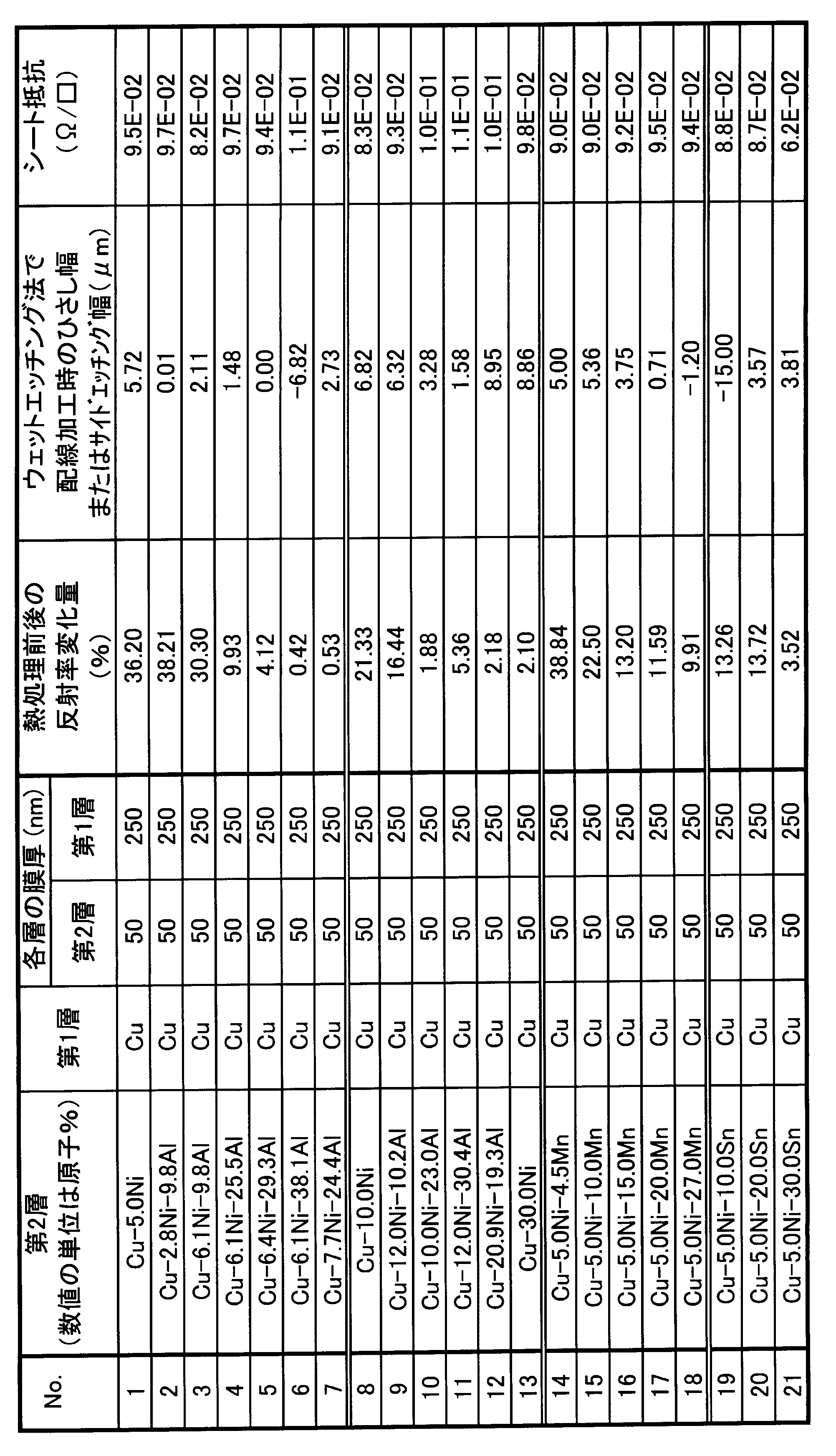
表2から次のことがわかる。No.1、8および13は、第2層がCuとNiからなりX元素を含んでいない例である。これらの例では、ひさし幅が大きくなりウェットエッチング加工性に劣った。No.1とNo.8は更に、耐酸化性にも劣る結果となった。
表2のNo.2~7およびNo.9~12は、第2層が、NiおよびX元素としてAlを含むCu-Ni-Al膜の例である。
これらの例のうち、No.2は、第2層のNi量が不足しており、NiとX元素の合計量も不足しているため耐酸化性に劣った。またNo.3および9は、第2層がX元素としてAlを含んでいるが、その含有量が不足しており、No.3ではNiとX元素の合計量も不足しているため、耐酸化性に劣った。No.9ではひさし幅が大きくなりウェットエッチング加工性にも劣る結果となった。No.12は、第2層のNi量が過剰であるため、ひさし幅が大きくなりウェットエッチング加工性に劣る結果となった。これに対し、表2のNo.4~7、10および11は、本発明で規定の要件を満たす例であり、優れた耐酸化性とウェットエッチング加工性を示すことがわかる。
表2のNo.14~18は、第2層が、NiおよびX元素としてMnを含むCu-Ni-Mn膜の例である。
これらの例のうち、No.14および15は、第2層がX元素としてMnを含んでいるが、その含有量が不足し、かつNiとX元素の合計量も不足しているため、耐酸化性に劣った。これに対し、表2のNo.16~18は、本発明で規定の要件を満たす例であり、優れた耐酸化性とウェットエッチング加工性を示すことがわかる。
表2のNo.19~21は、第2層が、NiおよびX元素としてSnを含むCu-Ni-Sn膜の例である。
これらの例のうち、No.19は、第2層がX元素としてSnを含んでいるが、その含有量が不足しているため、耐酸化性に劣った。これに対し、表2のNo.20および21は、本発明で規定の要件を満たす例であり、優れた耐酸化性とウェットエッチング加工性を示すことがわかる。
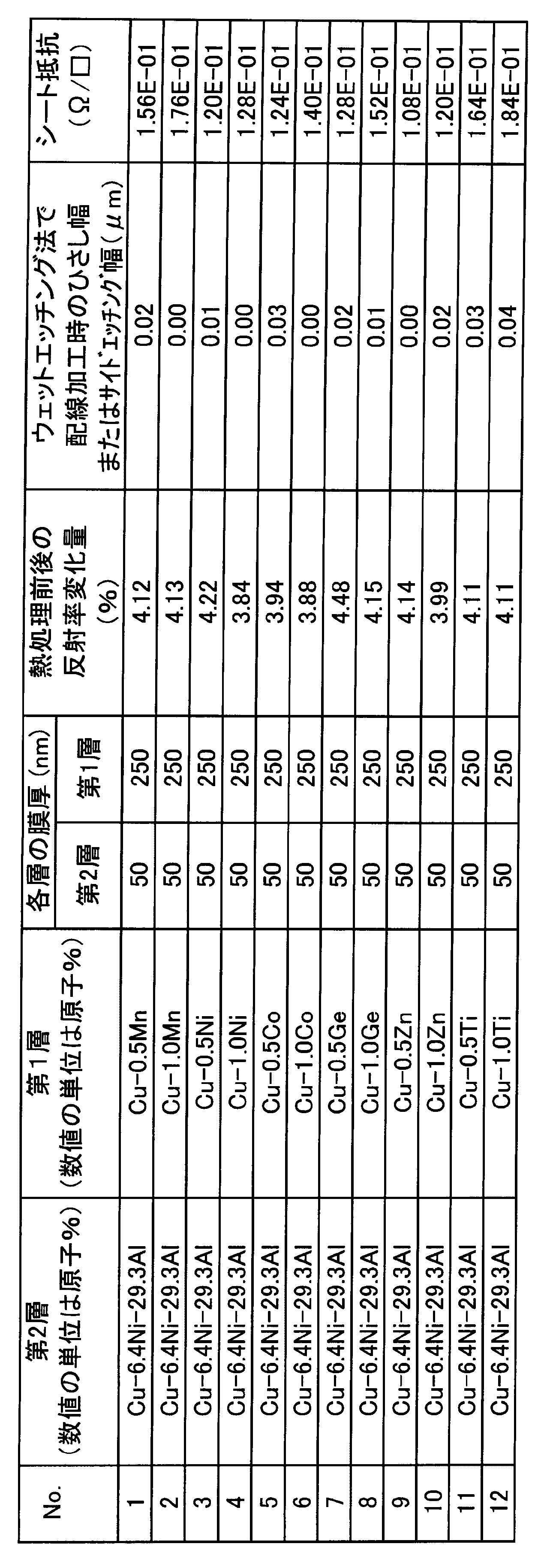
表3では、第2層を、Ni6.4原子%とAl29.3原子%を含むCu-Ni-Al膜で一定とし、第1層を種々のCu基合金膜として、第1層の成分組成がCu積層膜の特性に及ぼす影響を確認した。
表3の結果から、第1層として種々のCu基合金膜を用いたが、いずれの場合も優れた耐酸化性とウェットエッチング加工性が得られた。これらの結果から、Cu積層膜の耐酸化性とウェットエッチング加工性は、耐酸化保護層である第2層の成分組成による効果が主であり、第1層に種々のCu基合金膜を用いてもその特性は変わらないことがわかる。
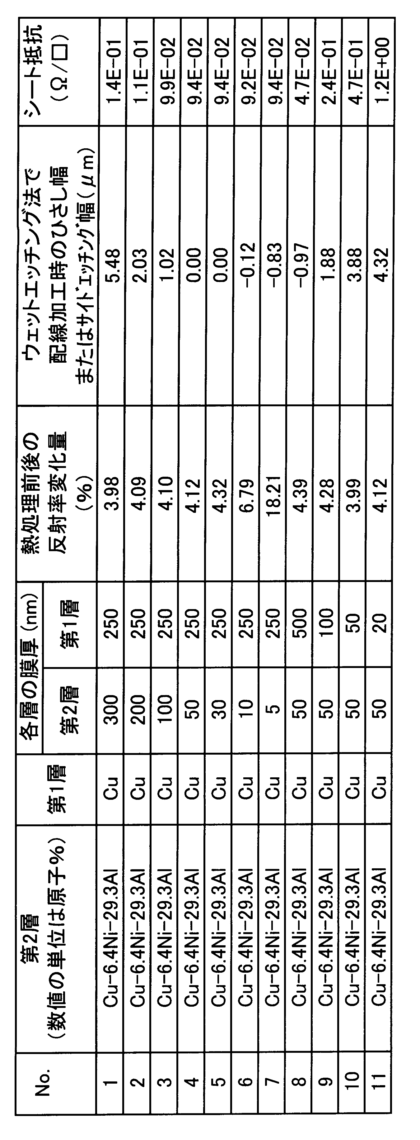
表4では、第1層を純Cu膜、第2層を、Ni6.4原子%とAl29.3原子%を含むCu-Ni-Al膜で一定とし、前記第1層と第2層の膜厚を変化させて、各層の膜厚依存性を確認した。その結果、表4のNo.1の通り、第2層の膜厚が推奨される上限200nmを超えた場合、ウェットエッチング加工時のひさし幅を十分に低減できず、良好なウェットエッチング加工性が得られなかった。また表4のNo.7の通り、第2層の膜厚が推奨される下限10nmを下回った場合には、熱処理前後の反射率変化量が大きくなり、十分な耐酸化性を確保することができなかった。これに対し、No.2~6、および8~11の通り、第2層の膜厚が推奨される範囲内にある例では、十分に優れた耐酸化性とウェットエッチング加工性が得られた。
1 第1層である純CuまたはCu基合金からなる膜
2 第2層であるCu-Ni-X膜
3 基板
4 密着層
2 第2層であるCu-Ni-X膜
3 基板
4 密着層
Claims (10)
- Niを3.0原子%以上19.0原子%以下含むと共に、
Al、Zn、MnおよびSnよりなる群から選択される1種のX元素を含み、残部がCuおよび不可避不純物からなり、かつ、
前記X元素の含有量は、下記式(1)から求められるx原子%以上であり、かつ、
前記X元素がZnまたはMnである場合、NiとX元素の合計量は20.0原子%以上であり、前記X元素がAlまたはSnである場合、NiとX元素の合計量は16.0原子%以上であることを特徴とするCu合金膜。
x=1.96×Ni+1.64・・・(1)
上記式(1)において、Niは、Cu合金膜中の原子%でのNi含有量を示す。 - 第1層として純CuまたはCu基合金からなる膜と、第2層として請求項1に記載のCu合金膜とを有することを特徴とするCu積層膜。
- 前記第2層の膜厚は10nm以上200nm以下である請求項2に記載のCu積層膜。
- 前記第1層におけるCu基合金は、Ti、Mn、Fe、Co、Ni、Ge、およびZnよりなる群から選択される少なくとも1種のZ元素を含み、残部がCuおよび不可避不純物からなる請求項2に記載のCu積層膜。
- 請求項2に記載のCu積層膜を用いた配線電極。
- 請求項4に記載のCu積層膜を用いた配線電極。
- 請求項2に記載のCu積層膜を用いた入力装置。
- 請求項4に記載のCu積層膜を用いた入力装置。
- 請求項2に記載のCu積層膜を用いたタッチパネルセンサー。
- 請求項4に記載のCu積層膜を用いたタッチパネルセンサー。
Priority Applications (2)
| Application Number | Priority Date | Filing Date | Title |
|---|---|---|---|
| CN201680003374.6A CN107075614A (zh) | 2015-02-19 | 2016-01-28 | Cu合金膜和Cu层叠膜 |
| KR1020177014556A KR20170078759A (ko) | 2015-02-19 | 2016-01-28 | Cu 합금막 및 Cu 적층막 |
Applications Claiming Priority (4)
| Application Number | Priority Date | Filing Date | Title |
|---|---|---|---|
| JP2015-030823 | 2015-02-19 | ||
| JP2015030823 | 2015-02-19 | ||
| JP2015-224068 | 2015-11-16 | ||
| JP2015224068A JP6250614B2 (ja) | 2015-02-19 | 2015-11-16 | Cu積層膜、およびCu合金スパッタリングターゲット |
Publications (1)
| Publication Number | Publication Date |
|---|---|
| WO2016132847A1 true WO2016132847A1 (ja) | 2016-08-25 |
Family
ID=56692136
Family Applications (1)
| Application Number | Title | Priority Date | Filing Date |
|---|---|---|---|
| PCT/JP2016/052499 Ceased WO2016132847A1 (ja) | 2015-02-19 | 2016-01-28 | Cu合金膜およびCu積層膜 |
Country Status (1)
| Country | Link |
|---|---|
| WO (1) | WO2016132847A1 (ja) |
Cited By (2)
| Publication number | Priority date | Publication date | Assignee | Title |
|---|---|---|---|---|
| CN106435261A (zh) * | 2016-11-28 | 2017-02-22 | 东莞市联洲知识产权运营管理有限公司 | 一种有超细晶组织的长寿命铜锰基合金靶材及其加工方法 |
| CN106480348A (zh) * | 2015-08-24 | 2017-03-08 | 湖南稀土院有限责任公司 | 一种灰控制棒用吸收体材料及其制备方法 |
Citations (4)
| Publication number | Priority date | Publication date | Assignee | Title |
|---|---|---|---|---|
| JPS62164893A (ja) * | 1986-01-14 | 1987-07-21 | Mitsubishi Chem Ind Ltd | 金色調鏡面製品 |
| JP2013120411A (ja) * | 2011-12-06 | 2013-06-17 | Kobe Steel Ltd | タッチパネルセンサー用Cu合金配線膜、及びその製造方法、並びにタッチパネルセンサー、及びスパッタリングターゲット |
| JP2014114481A (ja) * | 2012-12-10 | 2014-06-26 | Mitsubishi Materials Corp | 保護膜形成用スパッタリングターゲットおよび積層配線膜 |
| JP2015131998A (ja) * | 2014-01-14 | 2015-07-23 | 住友金属鉱山株式会社 | Cu合金配線、およびCu合金スパッタリングターゲット |
-
2016
- 2016-01-28 WO PCT/JP2016/052499 patent/WO2016132847A1/ja not_active Ceased
Patent Citations (4)
| Publication number | Priority date | Publication date | Assignee | Title |
|---|---|---|---|---|
| JPS62164893A (ja) * | 1986-01-14 | 1987-07-21 | Mitsubishi Chem Ind Ltd | 金色調鏡面製品 |
| JP2013120411A (ja) * | 2011-12-06 | 2013-06-17 | Kobe Steel Ltd | タッチパネルセンサー用Cu合金配線膜、及びその製造方法、並びにタッチパネルセンサー、及びスパッタリングターゲット |
| JP2014114481A (ja) * | 2012-12-10 | 2014-06-26 | Mitsubishi Materials Corp | 保護膜形成用スパッタリングターゲットおよび積層配線膜 |
| JP2015131998A (ja) * | 2014-01-14 | 2015-07-23 | 住友金属鉱山株式会社 | Cu合金配線、およびCu合金スパッタリングターゲット |
Cited By (3)
| Publication number | Priority date | Publication date | Assignee | Title |
|---|---|---|---|---|
| CN106480348A (zh) * | 2015-08-24 | 2017-03-08 | 湖南稀土院有限责任公司 | 一种灰控制棒用吸收体材料及其制备方法 |
| CN106435261A (zh) * | 2016-11-28 | 2017-02-22 | 东莞市联洲知识产权运营管理有限公司 | 一种有超细晶组织的长寿命铜锰基合金靶材及其加工方法 |
| CN106435261B (zh) * | 2016-11-28 | 2018-01-12 | 河北宏靶科技有限公司 | 一种有超细晶组织的长寿命铜锰基合金靶材及其加工方法 |
Similar Documents
| Publication | Publication Date | Title |
|---|---|---|
| KR101358529B1 (ko) | 전자부품용 적층 배선막 및 피복층 형성용 스퍼터링 타겟재 | |
| JP6250614B2 (ja) | Cu積層膜、およびCu合金スパッタリングターゲット | |
| JP2018174342A (ja) | 積層配線膜および薄膜トランジスタ素子 | |
| JP6361957B2 (ja) | 電子部品用積層配線膜および被覆層形成用スパッタリングターゲット材 | |
| TWI493624B (zh) | 電子零件用積層配線膜及被覆層形成用濺鍍靶材 | |
| CN112119179A (zh) | 层叠膜及Ag合金溅射靶 | |
| CN106796885B (zh) | 透明导电配线及透明导电配线的制造方法 | |
| WO2016132847A1 (ja) | Cu合金膜およびCu積層膜 | |
| CN102321832B (zh) | Cu电极保护膜用NiCu合金靶材以及叠层膜 | |
| TWI547575B (zh) | 金屬薄膜及金屬薄膜形成用鉬合金濺鍍靶材 | |
| TWI654339B (zh) | Wiring film | |
| WO2018147136A1 (ja) | 配線構造及びその製造方法、スパッタリングターゲット材、並びに酸化防止方法 | |
| TW201631168A (zh) | 銅基合金濺鍍靶材 | |
| JP5805708B2 (ja) | タッチパネルセンサー用配線膜、およびタッチパネルセンサー | |
| JP5756319B2 (ja) | Cu合金膜、及びそれを備えた表示装置または電子装置 | |
| JP2018087360A (ja) | 酸化物スパッタリングターゲット | |
| TW201928074A (zh) | 配線構造及靶材 | |
| JP2021064655A (ja) | 配線構造及びターゲット材 |
Legal Events
| Date | Code | Title | Description |
|---|---|---|---|
| 121 | Ep: the epo has been informed by wipo that ep was designated in this application |
Ref document number: 16752236 Country of ref document: EP Kind code of ref document: A1 |
|
| ENP | Entry into the national phase |
Ref document number: 20177014556 Country of ref document: KR Kind code of ref document: A |
|
| NENP | Non-entry into the national phase |
Ref country code: DE |
|
| 122 | Ep: pct application non-entry in european phase |
Ref document number: 16752236 Country of ref document: EP Kind code of ref document: A1 |