WO2016120913A1 - 電極付きカラーフィルタ基板、これを用いた表示装置、およびこれらの製造方法 - Google Patents
電極付きカラーフィルタ基板、これを用いた表示装置、およびこれらの製造方法 Download PDFInfo
- Publication number
- WO2016120913A1 WO2016120913A1 PCT/JP2015/003620 JP2015003620W WO2016120913A1 WO 2016120913 A1 WO2016120913 A1 WO 2016120913A1 JP 2015003620 W JP2015003620 W JP 2015003620W WO 2016120913 A1 WO2016120913 A1 WO 2016120913A1
- Authority
- WO
- WIPO (PCT)
- Prior art keywords
- layer
- electrode
- color filter
- resin layer
- filter substrate
- Prior art date
- Legal status (The legal status is an assumption and is not a legal conclusion. Google has not performed a legal analysis and makes no representation as to the accuracy of the status listed.)
- Ceased
Links
Images




Classifications
-
- G—PHYSICS
- G02—OPTICS
- G02B—OPTICAL ELEMENTS, SYSTEMS OR APPARATUS
- G02B5/00—Optical elements other than lenses
- G02B5/20—Filters
-
- G—PHYSICS
- G02—OPTICS
- G02F—OPTICAL DEVICES OR ARRANGEMENTS FOR THE CONTROL OF LIGHT BY MODIFICATION OF THE OPTICAL PROPERTIES OF THE MEDIA OF THE ELEMENTS INVOLVED THEREIN; NON-LINEAR OPTICS; FREQUENCY-CHANGING OF LIGHT; OPTICAL LOGIC ELEMENTS; OPTICAL ANALOGUE/DIGITAL CONVERTERS
- G02F1/00—Devices or arrangements for the control of the intensity, colour, phase, polarisation or direction of light arriving from an independent light source, e.g. switching, gating or modulating; Non-linear optics
- G02F1/01—Devices or arrangements for the control of the intensity, colour, phase, polarisation or direction of light arriving from an independent light source, e.g. switching, gating or modulating; Non-linear optics for the control of the intensity, phase, polarisation or colour
- G02F1/13—Devices or arrangements for the control of the intensity, colour, phase, polarisation or direction of light arriving from an independent light source, e.g. switching, gating or modulating; Non-linear optics for the control of the intensity, phase, polarisation or colour based on liquid crystals, e.g. single liquid crystal display cells
- G02F1/133—Constructional arrangements; Operation of liquid crystal cells; Circuit arrangements
- G02F1/1333—Constructional arrangements; Manufacturing methods
-
- G—PHYSICS
- G02—OPTICS
- G02F—OPTICAL DEVICES OR ARRANGEMENTS FOR THE CONTROL OF LIGHT BY MODIFICATION OF THE OPTICAL PROPERTIES OF THE MEDIA OF THE ELEMENTS INVOLVED THEREIN; NON-LINEAR OPTICS; FREQUENCY-CHANGING OF LIGHT; OPTICAL LOGIC ELEMENTS; OPTICAL ANALOGUE/DIGITAL CONVERTERS
- G02F1/00—Devices or arrangements for the control of the intensity, colour, phase, polarisation or direction of light arriving from an independent light source, e.g. switching, gating or modulating; Non-linear optics
- G02F1/01—Devices or arrangements for the control of the intensity, colour, phase, polarisation or direction of light arriving from an independent light source, e.g. switching, gating or modulating; Non-linear optics for the control of the intensity, phase, polarisation or colour
- G02F1/13—Devices or arrangements for the control of the intensity, colour, phase, polarisation or direction of light arriving from an independent light source, e.g. switching, gating or modulating; Non-linear optics for the control of the intensity, phase, polarisation or colour based on liquid crystals, e.g. single liquid crystal display cells
- G02F1/133—Constructional arrangements; Operation of liquid crystal cells; Circuit arrangements
- G02F1/1333—Constructional arrangements; Manufacturing methods
- G02F1/1335—Structural association of cells with optical devices, e.g. polarisers or reflectors
-
- G—PHYSICS
- G06—COMPUTING OR CALCULATING; COUNTING
- G06F—ELECTRIC DIGITAL DATA PROCESSING
- G06F3/00—Input arrangements for transferring data to be processed into a form capable of being handled by the computer; Output arrangements for transferring data from processing unit to output unit, e.g. interface arrangements
- G06F3/01—Input arrangements or combined input and output arrangements for interaction between user and computer
- G06F3/03—Arrangements for converting the position or the displacement of a member into a coded form
- G06F3/041—Digitisers, e.g. for touch screens or touch pads, characterised by the transducing means
-
- G—PHYSICS
- G09—EDUCATION; CRYPTOGRAPHY; DISPLAY; ADVERTISING; SEALS
- G09F—DISPLAYING; ADVERTISING; SIGNS; LABELS OR NAME-PLATES; SEALS
- G09F9/00—Indicating arrangements for variable information in which the information is built-up on a support by selection or combination of individual elements
-
- G—PHYSICS
- G09—EDUCATION; CRYPTOGRAPHY; DISPLAY; ADVERTISING; SEALS
- G09F—DISPLAYING; ADVERTISING; SIGNS; LABELS OR NAME-PLATES; SEALS
- G09F9/00—Indicating arrangements for variable information in which the information is built-up on a support by selection or combination of individual elements
- G09F9/30—Indicating arrangements for variable information in which the information is built-up on a support by selection or combination of individual elements in which the desired character or characters are formed by combining individual elements
-
- H—ELECTRICITY
- H01—ELECTRIC ELEMENTS
- H01B—CABLES; CONDUCTORS; INSULATORS; SELECTION OF MATERIALS FOR THEIR CONDUCTIVE, INSULATING OR DIELECTRIC PROPERTIES
- H01B5/00—Non-insulated conductors or conductive bodies characterised by their form
- H01B5/14—Non-insulated conductors or conductive bodies characterised by their form comprising conductive layers or films on insulating-supports
Definitions
- the present invention relates to a color filter substrate with an electrode, a display device using the same, and a manufacturing method thereof.
- the present invention relates to a color filter substrate with an electrode in which a touch sensor operating in a capacitive manner is integrated, a display device using the same, and a method for manufacturing the same.
- touch panel system examples include a resistance film type and a capacitance type.
- the touch position is detected by contacting the upper and lower electrodes.
- the capacitance type the touch position is detected by a change in the surface capacitance when a fingertip or the like touches.
- the sensor of the electrostatic capacity type touch panel is generally used as an out-cell structure which is produced as an electrode pattern on a resin substrate such as a PET film or a glass substrate and is arranged outside the display structure.
- Patent Document 1 Patent Document 1
- Patent Document 2 Patent Document 3
- JP 2007-178758 A Japanese Patent No. 4816668 Japanese Patent No. 4584342 JP-A-6-273936 JP-A-10-98266 Japanese Patent Laid-Open No. 2003-122004 Japanese Patent Laid-Open No. 48-89003 Japanese Patent Application Laid-Open No. 60-3625 JP-A-63-27829
- the in-cell structure requires a touch sensor circuit to be incorporated in the TFT substrate which is a display display drive circuit.
- the design and process are complicated and the yield of non-defective products is accompanied.
- the on-cell structure forms a touch sensor in a cell state in which liquid crystal is sealed, particularly in the case of a liquid crystal display. For this reason, there has been a problem in process design in consideration of damage to the liquid crystal due to process conditions such as heat.
- a color filter substrate with electrodes it is required to further reduce the resistivity of the electrode layer.
- various types of metal elements can be used for the electrode layer of the color filter substrate with electrodes depending on the application.
- One object of the present invention is to provide a color filter substrate with electrodes that operates stably with high yield and is compatible with various display designs, a display device using the same, and a manufacturing method thereof. It is.
- another object of the present invention is to solve the above-mentioned problems of the prior art in manufacturing a display in which a touch sensor is integrated.
- An example of means for solving the problems of the present invention includes a color filter layer, a transparent substrate, a cured resin layer, and an electrode layer in this order,
- the cured resin layer is formed by irradiating and curing the photosensitive resin layer,
- the cured resin layer and the electrode layer include a predetermined pattern that is substantially the same in plan view, It is a color filter substrate with an electrode in which the electrode layer is formed of a substantially bulk metal or conductive metal oxide.
- the electrode layer is preferably formed of at least one selected from the group consisting of gold, silver, copper, aluminum, iron, titanium, molybdenum, indium, tin, niobium, and oxides thereof. .
- the electrode layer preferably has a resistivity of 0.01 ⁇ / ⁇ or more and 10 ⁇ / ⁇ or less.
- it further comprises a further cured resin layer and a further electrode layer following the order, wherein the further cured resin layer and the further electrode layer have substantially the same further predetermined pattern, and The predetermined pattern may cross the predetermined pattern.
- the electrode layer may be a part of a constituent element of a touch sensor for detecting a touch position.
- a blackening layer having an antireflection function or a blackening function may be formed on the upper surface of the electrode layer.
- a transparent insulating layer may be formed on the upper surface of the electrode layer.
- Another example of means for solving the problems of the present invention is a display device using the above-described color filter substrate with electrodes.
- Still another example of means for solving the problems of the present invention is a step of preparing a laminate in which a color filter layer, a transparent substrate, a photosensitive resin layer, and an electrode precursor layer are laminated in this order, Irradiating the photosensitive resin layer with light through a photomask from the electrode precursor layer side; Conducting the conductive treatment of the electrode precursor layer; The step of developing the photosensitive resin layer, wherein the electrode precursor layer is selected from the group consisting of metal nanoparticles having a particle size of 100 nm or less, metal oxide nanoparticles having a particle size of 100 nm or less, and a metal complex It is a manufacturing method of the color filter substrate with an electrode containing one.
- the conductive treatment is performed by the light energy of the light irradiation, and the light irradiation step and the conductive treatment step are performed simultaneously.
- the conductive treatment may be performed by heat treatment or further light irradiation.
- the metal nanoparticles are preferably formed from at least one selected from the group consisting of gold, silver, copper, aluminum, iron, titanium, molybdenum, indium, tin, and niobium.
- the metal oxide nanoparticles are preferably formed of at least one oxide selected from the group consisting of gold, silver, copper, aluminum, iron, titanium, molybdenum, indium, tin, and niobium.
- the metal complex is preferably at least one selected from the group consisting of a gold complex, a silver complex, and a copper complex.
- Still another example of means for solving the problems of the present invention is a method for manufacturing a display device, including the above-described method for manufacturing a color filter substrate with electrodes.
- a TFT substrate is bonded in advance to the surface of the color filter layer opposite to the transparent substrate,
- the display device manufacturing method further includes a step of forming an electrode layer by the conductive treatment and electrically connecting the electrode layer to a drive circuit of a touch sensor.
- a color filter substrate with an electrode that operates stably with a high yield and is compatible with various display designs, a display device using the same, and a manufacturing method thereof.
- FIG. 1 shows an example of a schematic partial longitudinal sectional view of a color filter substrate with electrodes of the present invention.
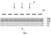
- FIG. 2 shows an example of a schematic partial cross-sectional view showing a step of irradiating the photosensitive resin layer with light from the photomask side.
- FIG. 3 shows another example of a schematic partial longitudinal sectional view of the color filter substrate with an electrode of the present invention.
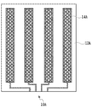
- FIG. 4 shows an example of a schematic partial top view showing the electrode shape of the color filter substrate with electrodes of the present invention.
- FIG. 5 shows another example of a schematic partial top view showing the electrode shape of the color filter substrate with electrodes of the present invention.
- FIG. 6 shows an example of a schematic partial longitudinal sectional view of a display device using the color filter substrate with an electrode of the present invention.
- FIG. 7 shows another example of a schematic partial longitudinal sectional view of a display device using the color filter substrate with an electrode of the present invention.
- FIG. 8 shows an example of a schematic partial longitudinal sectional view of an organic EL display using the electrode-attached color filter substrate of the present invention.
- FIG. 1 shows an example of a schematic partial longitudinal sectional view of a color filter substrate with electrodes of the present invention.
- the color filter substrate 10 with an electrode shown in FIG. 1 includes a color filter layer 11, a transparent substrate 12, a cured resin layer 13, and an electrode layer 14 in this order.
- the transparent substrate 12 glass or a plastic film can be used.
- the transparent substrate 12 is not particularly limited as long as it has sufficient strength in the film forming step and the subsequent step, has excellent transparency, and has good surface smoothness.
- As the glass alkali-free glass for display is preferably used.
- the plastic film include polyethylene terephthalate film, polybutylene terephthalate film, polyethylene naphthalate film, polycarbonate film, polyethersulfone film, polysulfone film, polyarylate film, cyclic polyolefin film, and polyimide film. Further, since the transparent substrate 12 is typically used for a color filter of a display device, it needs to have high transparency.
- the transparent substrate 12 having a total light transmittance of 85% or more is preferably used.
- the transparent substrate 12 may be subjected to corona treatment, low temperature plasma treatment, ion bombardment treatment, chemical treatment, etc. as pretreatment in order to improve adhesion with each layer.
- a color filter layer 11 is formed on one surface of the transparent substrate 12.
- the color filter layer 11 typically refers to a layer including at least a black matrix and colored layers of each color of red, green, and blue.
- the color filter layer 11 can be formed by applying a colored photosensitive ink by a method such as spin coating, spinless coating, and inkjet, and then exposing and baking. Further, a transparent electrode may be formed so as to cover the black matrix and the colored layer.
- the colored layer is made of, for example, an acrylic resin having a thickness of 0.5 to 3.0 ⁇ m in which pigments of various colors are dispersed.
- the black matrix is formed of, for example, an acrylic resin having a thickness of 0.5 to 3.0 ⁇ m in which a black pigment is dispersed or a metal film having a thickness of 10 to 200 nm.
- a yellow, cyan, magenta, or white (colorless) layer may be used as the color filter layer.
- the transparent electrode is made of, for example, ITO having a thickness of 10 to 200 nm. Further, a transparent resin layer may be formed on the color filter layer 11 for the purpose of flattening and protection.
- a cured resin layer 13 is formed on the other surface of the transparent substrate 12.
- the cured resin layer 13 is a layer obtained by exposing and curing a photosensitive resin layer (also referred to as an unexposed photosensitive resin layer) 13x described later.
- the photosensitive resin layer 13x may be a negative photosensitive resin or a positive photosensitive resin.
- the negative photosensitive resin is generally composed of a resin material serving as a binder, a photopolymerizable material, and a material containing at least a photopolymerization initiator, but is not particularly limited.
- materials described in Patent Documents 4 to 6 can be used.
- the positive photosensitive resin is generally formed from a material containing an alkali-soluble resin material, a photoacid generating material, an acid-decomposable functional group-containing compound, etc., but is not particularly limited.
- the positive photosensitive resin for example, materials described in Patent Documents 7 to 9 can be used.
- the photosensitive resin layer 13x is coated with the above materials by a known coating method such as a die coater, curtain flow coater, roll coater, reverse roll coater, gravure coater, knife coater, bar coater, spin coater, micro gravure coater, It can be formed by drying.
- the film thickness of the photosensitive resin layer 13x is preferably 0.1 ⁇ m or more and 25 ⁇ m or less, for example, 5 ⁇ m, but is not limited thereto. Since the photosensitive resin layer 13x has almost no change in film thickness before and after curing, the film thickness after curing will be described hereinafter. When the film thickness is 25 ⁇ m or less, high-definition pattern formation becomes easy.
- the photosensitive resin layer 13x has a portion soluble in the developer and an insoluble portion by light irradiation through the photomask 15. A portion soluble in the developer of the photosensitive resin layer 13x is dissolved by development, and a pattern of the cured resin layer 13 composed of an insoluble portion can be formed.
- the developer can be appropriately selected depending on the type of the photosensitive resin layer 13x or its material, and can generally be an alkaline aqueous solution or an organic solvent.
- the electrode layer 14 is a layer formed by subjecting the electrode precursor layer 14x to a conductive treatment.
- the electrode precursor layer 14x contains metal nanoparticles or metal oxide nanoparticles having a particle size of 100 nm or less, for example, a particle size of 60 nm.
- the particle diameter is an average particle diameter (conforming to JIS Z 8825: 2013) measured by a laser diffraction method. Since the metal nanoparticles or metal oxide nanoparticles have a particle diameter of 100 nm or less, the resistance is sufficiently low as a color filter substrate.
- the resistance is 0.01 ⁇ / ⁇ or more and 10 ⁇ / ⁇ or less, which is clearly different from the resistivity (100 ⁇ / ⁇ or more and 500 ⁇ / ⁇ or less) of conventional metal nanowires and carbon nanotubes.
- the metal nanoparticles or metal oxide nanoparticles can be used as a transparent electrode layer having properties equivalent to those of a bulk metal by light firing or heat firing and exhibiting low resistance.
- metal nanoparticles or metal oxide nanoparticles have the advantage of being superior in terms of light transmittance when formed in a mesh shape with a line width of 10 ⁇ m or less, compared to normal particles.
- the metal nanoparticles or metal oxide nanoparticles are preferably particles containing at least one element selected from the group consisting of gold, silver, copper, aluminum, iron, titanium, molybdenum, indium, tin, and niobium.
- Specific examples of the metal nanoparticles or metal oxide nanoparticles include copper nanoparticles, silver nanoparticles, indium tin oxide nanoparticles, titanium nanoparticles, and the like.
- the electrode precursor layer 14x contains a metal complex.
- the metal complex include a gold complex, a silver complex, and a copper complex.
- the electrode precursor layer 14x has a light transmittance that allows the photosensitive resin layer 13x to be exposed through the electrode precursor layer 14x.
- a color filter substrate with electrodes having a transparent substrate, a cured resin layer, and an electrode layer in this order and having an extremely low resistance (for example, 0.01 ⁇ / ⁇ or more and 10 ⁇ / ⁇ or less).
- the concentration of the particles is increased in the electrode precursor layer, the light transmittance is lost, so that exposure through the electrode precursor layer becomes difficult.
- the concentration of the particles is lowered in the electrode precursor layer, it becomes difficult to form the electrode layer itself.
- nanowires When nanowires are aggregated, they form a network structure, but exhibit high resistance (for example, 150 ⁇ / ⁇ ).
- high resistance for example, 150 ⁇ / ⁇ .
- metal nanoparticles, metal oxide nanoparticles or metal complexes are aggregated to such an extent that they have optical transparency (at first glance low concentration). In other words, it has been found that the conductive layer can function as an extremely low resistance electrode layer.
- a dispersion ink or paste such as a metal of the metal nanoparticles, an oxide thereof, an ion thereof, or a complex thereof is used in an aqueous solution or an organic solvent. Those dissolved or dispersed can be used.
- the concentration (solid content concentration) of the metal nanoparticles or metal oxide nanoparticles in the electrode precursor layer material is 10 wt% or more and 90 wt% or less, for example 50 wt%, based on the electrode precursor layer material.
- the concentration (solid content concentration) of the metal nanoparticles or metal oxide nanoparticles in the electrode precursor layer material is appropriately selected according to the properties of the ink and the target film thickness.
- the electrode precursor layer material can be applied by a known coating method such as a die coater, curtain flow coater, roll coater, reverse roll coater, gravure coater, knife coater, bar coater, spin coater, or micro gravure coater. Thereafter, the electrode precursor layer 14x can be formed by drying or heating.
- the film thickness of the electrode precursor layer 14x varies depending on the solid content concentration and the film thickness after firing, but is formed to be, for example, 500 nm or more and 10 ⁇ m or less. Since the film thickness of the electrode precursor layer 14x is 500 nm or more, it is easy to form a film, and since it is 10 ⁇ m or less, it is difficult to crack due to stress.
- the electrode precursor layer 14x is typically non-conductive when the coating film is formed.
- the film thickness of the electrode layer 14 is 100 nm or more and 300 nm or less, for example, 200 nm.
- the film thickness of the electrode layer 14 is 100 nm or more, an effect that the film is easily formed is obtained, and when it is 300 nm or less, an effect that cracks hardly occur due to stress is obtained.
- the electrode layer 14 is formed by exposing and developing the photosensitive resin layer 13x to form a pattern, or at the same time as exposing the photosensitive resin layer 13x, and simultaneously firing the electrode precursor layer 14x to be conductive, for example.
- the firing method can be appropriately selected according to the material and properties of the electrode precursor layer 14x.
- a hot air oven, an IR heater, a hot plate, or the like can be used for the thermal firing, and a xenon flash lamp is generally used for the light firing.
- the electrode precursor layer 14x is formed so as to transmit a certain amount of light in the sensitive wavelength region of the photosensitive resin layer 13x. good.
- the photosensitive resin layer 13x and the electrode precursor layer 14x are formed on the transparent substrate 12 on which the color filter layer 11 is formed.
- the photosensitive resin layer 13x and the electrode precursor layer 14x are first formed on the surface of the transparent substrate 12 where the color filter layer 11 is not formed.
- the photosensitive resin layer 13x and the electrode precursor layer 14x may be formed on the transparent substrate 12 in this order.
- this is bonded together to the transparent substrate 12 using a laminator etc.,
- the said support film base You may form by peeling a material.
- the support film substrate is not particularly limited as long as it is a film having good releasability.
- a support film base is formed of a thin film of a resin containing a silicone material or a fluorine material for imparting releasability to a film substrate such as polyethylene, polypropylene, polyethylene terephthalate (PET), polycarbonate (PC), etc. It is suitably used as a material. If there are irregularities on the surface of the support film substrate, problems such as transfer of irregularities to the photosensitive resin layer 13x after peeling, or defects in peeling of the support film substrate may occur. Therefore, the surface of the support film substrate is preferably smooth.
- the cured resin layer 13 and the electrode layer 14 may be formed on a color filter substrate (a laminate of the color filter layer 11 and the transparent substrate 12) in advance according to heat resistance and then manufactured for display. Or you may form the cured resin layer 13 and the electrode layer 14 in the back surface (surface by the side of the transparent substrate 12 of the said laminated body) after producing a display. When the latter process is used, it is possible to reduce the thickness by dissolving both the glass of the color filter substrate (transparent substrate 12) and the glass to be the TFT substrate in a cell display with a chemical solution such as hydrofluoric acid.
- the cured resin layer 13 and the electrode layer 14 may be formed in a display device in which the transparent substrate 12 on which the color filter layer 11 is formed is bonded to a TFT substrate to form a cell.
- the photosensitive resin layer 13x and the electrode precursor layer 14x formed on the transparent substrate 12 are irradiated with light through the photomask 15 as indicated by an arrow P in FIG.
- the photomask 15 can be formed by a conventionally known method.
- FIG. 2 shows an example in which light irradiation through a photomask 15 is performed on a laminated body 10x in which a color filter layer 11, a transparent substrate 12, a photosensitive resin layer 13x, and an electrode precursor layer 14x are laminated in this order.
- the light irradiation can be performed using a light source capable of irradiating a light wavelength to which a photopolymerization initiator, a photoacid generating material, or the like of the photosensitive resin layer 13x is sensitive.
- an ultra high pressure mercury lamp, a high pressure mercury lamp, a xenon lamp, a metal halide lamp, or the like can be used.
- Energy of light irradiation 1000 mJ / cm 2 or more 8000 mJ / cm 2 or less, such as 4000 mJ / cm 2.
- the energy of light irradiation is 1000 mJ / cm 2 or more, an effect is obtained that the exposure of the photosensitive resin layer 13x and the electroconductivity of the electrode precursor layer 14x by light baking are sufficiently promoted.
- the energy of light irradiation is 8000 mJ / cm 2 or less, the effect of suppressing the oxidation of the conductive electrode layer 14 and the influence of heat on the base can be obtained.
- a pattern in which the electrode precursor layer 14x or the electrode layer 14 is formed on the cured resin layer 13 can be produced by developing the dissolved portion of the cured resin layer 13 with a developer.
- the electrode precursor layer 14x may be made conductive by light baking with xenon flash or the like, or heat baking with a hot air oven or IR heater, to form the electrode layer 14.
- a light irradiation apparatus capable of light baking such as a xenon flash is used.
- the electrode precursor layer 14x may be used as the conductive electrode layer 14 by simultaneously performing exposure of the photosensitive resin layer 13x and light baking of the electrode precursor layer 14x.
- the cured resin layer 13 and the electrode layer 14 have substantially the same predetermined pattern in plan view, and the electrode layer 14 is formed on the convex portion of the pattern of the cured resin layer 13. .
- the cured resin layer and the electrode layer have substantially the same predetermined pattern in plan view that the cured resin layer and the electrode layer have substantially the same predetermined pattern with respect to the cross-sectional shape. Meaning, or the meaning that the surface shape of the predetermined pattern of the electrode layer is substantially the same as the surface shape of the predetermined pattern of the cured resin layer.
- substantially the same includes the meaning that a difference caused by an error or the like at the time of forming a layer or pattern is also included.
- FIG. 3 shows another example of a schematic partial longitudinal sectional view of the color filter substrate with an electrode of the present invention.
- members that are the same as or similar to the members in FIG. 1 are given the same reference numerals, or added with reference numerals A, and description thereof is omitted.
- a further cured resin layer 23 and a further electrode layer 24 are formed.
- the formation method of the further cured resin layer 23 and the further electrode layer 24 can be performed similarly to the cured resin layer 13 and the electrode layer 14, respectively.
- the electrode layer 14 and the further electrode layer 24 can have a pseudo diamond pattern in plan view.
- the inside of the pseudo diamond pattern is composed of thin line-shaped electrodes, and a light-transmissive electrode pattern can be obtained by setting the thin line width to 5 ⁇ m or less.
- the electrode-provided color filter substrate 10 or 20 produced as described above may have a plurality of surfaces on one glass substrate. In this case, it is possible to efficiently manufacture a plurality of pieces by cutting the color filter substrate with electrodes 10 or a state in which the color filter substrate 10 is bonded to the TFT substrate 30 into pieces. Examples of the singulation method include diamond cutter scribe processing, dicing processing, water jet processing, etching processing, and laser processing. After singulation, the wiring connected to the electrode layer 14 or 24 is connected to a driving IC or the like via an anisotropic conductive adhesive (ACF) and a printed circuit board (FPC), and operates as a capacitive touch panel Can be made.
- ACF anisotropic conductive adhesive
- FPC printed circuit board
- the FPC is thermocompression bonded to the wiring drawn from the electrode layer 14 or the electrode layer 24 via the ACF, and the FPC is connected to the drive IC of the touch sensor.
- the TFT substrate 30 is connected to the drive IC and the FPC and is connected to the drive circuit.
- the electrode layer 14 is paired with an electrode (not shown) formed on another layer to form a capacitive touch sensor. Can be used.
- a plan view of the electrode layer 14 can use a pseudo-rectangular pattern as shown in FIG.
- the electrode layer 14 shown in FIG. 4 is connected to a drive circuit via a wiring portion extended from the end (not shown), and forms a capacitance with the electrodes formed in the other layers described above. Functions as a capacitive touch sensor.
- the electrodes formed on the other layers can be formed by appropriately selecting, for example, the inside of the TFT circuit on the TFT substrate, the inside of the color filter on the color filter substrate, the cover glass, or the polarizing plate.
- FIG. 5 shows another example of a schematic partial top view showing the electrode shape of the color filter substrate with electrodes of the present invention.
- the electrode layer 14A and the further electrode layer 24A shown in FIG. 5 are connected to a drive circuit via a wiring portion extended from the end portion, and function as a capacitive touch sensor.
- Examples of the display device having the electrode-attached color filter substrate of the present invention include a liquid crystal display, an organic EL display, electronic paper, a MEMS display, a reflective or transflective liquid crystal display, and the like.
- Examples of display devices having a liquid crystal layer include those having the structure shown in FIG. 6 or FIG.
- a liquid crystal layer 40 is formed between the color filter substrate with electrode 10 and the TFT substrate 30.
- a liquid crystal layer 40 is formed between the color filter substrate with electrode 20 and the TFT substrate 30.
- a polarizing plate 50 and a cover glass 70 are sequentially formed on the surface of the color filter substrate with electrode 20 opposite to the liquid crystal layer 40.
- a polarizing plate 50 and a backlight 60 are sequentially formed on the surface of the TFT substrate 30 opposite to the liquid crystal layer 40.
- a plurality of scanning lines are formed on the TFT substrate 30 at regular intervals.
- a plurality of signal lines are formed at regular intervals on the scanning lines.
- the scanning line and the signal line are arranged so as to intersect with each other via an insulating film.
- a thin film transistor (TFT) that is a switching element is disposed in the vicinity of the intersection of the scanning line and the signal line.
- a display signal is supplied from the signal line to the pixel electrode via the TFT.
- the pixel electrode is formed from a transparent conductive film such as ITO, for example.
- the display area of the liquid crystal display element is composed of a plurality of pixels. The display area is usually formed in a shape close to a rectangle. Further, a frame area provided so as to surround the display area is arranged in the display element.
- the liquid crystal layer 40 can be formed using a known material, and is sealed between the color filter substrate with electrodes 10 or 20 and the TFT substrate 30.
- an alignment film can be formed on the surface of the color filter layer 11 of the electrode-attached color filter substrate 10 or 20 and the TFT substrate 30 by a method such as flexographic printing, and a rubbing treatment can be performed. Thereafter, by enclosing the liquid crystal layer 40, the liquid crystal molecules can be aligned in a certain direction.
- the polarizing plates 50 arranged on both surfaces of the liquid crystal cell have absorption axes in directions almost orthogonal to each other.
- the lighting, gray scale, and extinguishing of each pixel are determined by the direction of linearly polarized light controlled by the liquid crystal.
- the backlight 60 is attached to the polarizing plate 50 on the side opposite to the visual recognition (back side) with an adhesive or the like.
- the backlight 60 irradiates the polarizing plate 50 with planar light.
- the backlight 60 the thing of the general structure provided with the light source, the light-guide plate, the prism sheet etc. is used, for example.
- the cover glass 70 may be adhered to the four sides of the polarizing plate 50 on the viewing side or the four sides of the display housing with a double-sided tape or the like, or the entire surface including the display portion of the liquid crystal display is bonded using a transparent optical adhesive. Also good.
- the cover glass 70 is made of chemically strengthened glass or transparent resin. Thereby, the display device 100 or 200 is completed.
- the display devices 100 and 200 When the display devices 100 and 200 are manufactured, a liquid crystal cell formed of, for example, the color filter substrate with electrodes 10 or 20, the TFT substrate 30, and the liquid crystal layer 40 is sandwiched between the polarizing plate layers 50. Thereafter, the backlight 60 is disposed on the back surface, and the cover glass 70 is disposed on the display surface.
- the display device 100 or 200 that is, a liquid crystal display integrated with a capacitive touch sensor can be provided.
- FIG. A white organic light emitting layer 80 is formed on the TFT substrate 30 on which TFTs are formed on glass.
- an organic EL light emitting element structure is formed by forming a transparent upper electrode layer.
- the electrode-attached color filter substrate 20 is bonded through a sealant having moisture absorption ability.
- the organic EL display 300 can be obtained by forming a layer that doubles as a capacitive touch sensor, a color filter, and sealing glass.
- the white organic light emitting layer 80 includes a hole transport layer, a hole injection layer, a light emitting layer, an electron injection layer, an electron transport layer, and the like, and can be formed using a known material.
- Example 1 A display device corresponding to the display device 200 of FIG. 7 was produced.
- Aluminosilicate glass was used as the transparent substrate.
- the black photosensitive coloring composition was applied with a spin coater, dried on a hot plate at 100 ° C. for 5 minutes to dry the coating film. Thereafter, exposure was performed through a photomask having a desired opening at 100 mJ / cm 2 using a high-pressure mercury lamp as a light source. Thereafter, shower development was carried out with a 0.2% by mass aqueous sodium hydrogen carbonate solution for 30 seconds. After washing with water, heat treatment was performed at 230 ° C. for 30 minutes in a hot air circulation oven to form a black matrix pattern. Thereafter, except that the type of the photosensitive coloring composition was changed, red, green and blue patterns were sequentially formed to form a color filter layer. Thus, a color filter substrate including the transparent substrate and the color filter layer was formed.
- an alignment film was formed by printing on the surface of the TFT substrate on which the color filter layer of the color filter substrate and the TFT circuit were formed. Then, it baked at 230 degreeC and performed the rubbing process. Thereafter, the color filter substrate and the TFT substrate were bonded together with a sealing material. Thus, a liquid crystal material was injected into the gap to form a liquid crystal layer.
- a photosensitive resin layer and an electrode precursor layer were formed on the surface of the transparent substrate where the color filter layer was not formed.
- the photosensitive resin layer and the electrode precursor layer were formed by pasting together a support film substrate with a laminator.
- a support film substrate a PET film in which a silicone resin was formed with a thickness of about 200 nm was prepared.
- Copper nanoparticles having an average particle diameter of 60 nm were applied to the silicone resin surface and dried to form a thickness of 150 nm.
- the copper nanoparticles were applied by slit die coating using an alcohol-based dispersion ink having a solid content concentration of 50 wt% and dried at 120 ° C.
- a photosensitive resin material manufactured by Tokyo Ohka Kogyo Co., Ltd.
- a photosensitive resin material manufactured by Tokyo Ohka Kogyo Co., Ltd.
- the obtained photosensitive resin material was bonded to a PET film as a cover film.
- the copper nanoparticle and photosensitive resin material laminated body which were previously formed in the support film base material were bonded together to the surface in which the color filter layer of the transparent substrate was not formed, after peeling a cover film. Thereafter, light irradiation was performed at 4000 mJ / cm 2 using a high-pressure mercury lamp through a photomask, and the photosensitive resin layer of the light irradiated portion was cured. Subsequently, shower development was carried out with a 0.2% by mass aqueous sodium hydrogen carbonate solution for 30 seconds, followed by washing with water, followed by heat treatment at 120 ° C. for 30 minutes in a hot air oven. Thus, copper nanoparticles were formed as a conductive electrode layer. At this time, the plan view of the electrode layer was formed in a diamond shape with a mesh structure as shown in FIG. The line width of the mesh structure was 4 ⁇ m, and the distance between the lines was 250 ⁇ m.
- a further photosensitive resin layer and a further electrode precursor layer were formed in the same manner.
- the plan view of the electrode layer and the further electrode layer has a mesh structure as shown in FIG.
- a further electrode layer was arranged at a distance of 120 ⁇ m so that the diamond shape of the electrode layer did not overlap the diamond shape of the electrode layer.
- the line width and distance between lines of the mesh structure of the further electrode layer were the same as those of the electrode layer.
- the FPC terminal and the wiring connected to the electrode layer and the further electrode layer were electrically connected via the ACF to connect the touch sensor driving IC.
- the FPC and the liquid crystal driving IC were connected also at the end of the TFT substrate.
- the polarizing plate was affixed on the upper surface of the further electrode layer of a color filter board
- a backlight was attached to the polarizing plate on the anti-visible (back) side.
- a chemically strengthened glass was bonded as a cover glass on the viewing side (upper surface) polarizing plate using an optical adhesive.
- a liquid crystal display integrated with a capacitive touch sensor was produced. The display was good and the touch sensor could be operated well.
- the color filter substrate with electrodes of the present invention can be used as a touch panel display in which, for example, a liquid crystal display or organic EL display using a color filter and a capacitive touch sensor are integrated.
- the electrode-attached color filter substrate of the present invention can be further used as a display and user interface for smartphones, tablets, notebook PCs, and the like.
Landscapes
- Physics & Mathematics (AREA)
- Engineering & Computer Science (AREA)
- General Physics & Mathematics (AREA)
- Theoretical Computer Science (AREA)
- Nonlinear Science (AREA)
- Optics & Photonics (AREA)
- Mathematical Physics (AREA)
- Chemical & Material Sciences (AREA)
- Crystallography & Structural Chemistry (AREA)
- General Engineering & Computer Science (AREA)
- Liquid Crystal (AREA)
- Human Computer Interaction (AREA)
- Optical Filters (AREA)
- Devices For Indicating Variable Information By Combining Individual Elements (AREA)
Abstract
カラーフィルタ層、透明基板、硬化樹脂層、および電極層をこの順に備え、前記硬化樹脂層が感光性樹脂層を光照射して硬化させることにより形成されており、前記硬化樹脂層および前記電極層が平面視で実質的に同一の所定のパターンを含み、前記電極層が、実質的にバルクの金属または導電性金属酸化物から形成されている、電極付きカラーフィルタ基板である。
Description
本発明は、電極付きカラーフィルタ基板、これを用いた表示装置、およびこれらの製造方法に関する。好適には、本発明は、静電容量方式で動作するタッチセンサが一体となった電極付きカラーフィルタ基板、これを用いた表示装置、およびこれらの製造方法に関する。
近年、様々な電子機器のディスプレイ上に、入力デバイスとして透明なタッチパネルが用いられている。タッチパネルの方式としては、抵抗膜式、静電容量式などが挙げられる。抵抗膜式では上下の電極が接触することでタッチ位置を検出する。また静電容量式では指先などが触れた際の表面の静電容量の変化でタッチ位置を検出する。
静電容量式タッチパネルのセンサーはPETフィルムなどの樹脂基板やガラス基板に電極パターンとして作製し、ディスプレイ構造の外側に配置されるアウトセル構造が一般的に用いられている。(特許文献1)
一方、近年ではタッチセンサをディスプレイ構造に組み込むインセル構造やオンセル構造が採用され始めており、タッチセンサ付きディスプレイをより薄型・軽量化する取り組みがなされている。(特許文献2、特許文献3)
しかしながら、インセル構造はディプレイ表示の駆動回路であるTFT基板にタッチセンサの回路を組み込む必要がある。この場合、従来から設計やプロセスの煩雑さとそれに伴う良品収率の悪化が伴うことが指摘されていた。またオンセル構造は、特に液晶ディスプレイの場合、液晶を封入したセルの状態でタッチセンサを形成する。そのため、熱などのプロセス条件による液晶へのダメージを考慮したプロセス設計に課題があった。
特に、電極付きカラーフィルタ基板においては、電極層の抵抗率を更に低下させることが求められる。また、電極付きカラーフィルタ基板においては、全体の膜厚を更に小さく(薄く)することが求められる。更に、電極付きカラーフィルタ基板の電極層は、用途に応じて様々な種類の金属元素を利用可能であることが好ましい。
本発明の1つの目的は、歩留まり良く、安定に動作し、様々なディスプレイ設計に対応する汎用性を備えた電極付きカラーフィルタ基板、これを用いた表示装置、およびこれらの製造方法を提供することである。好適には、本発明のもう1つの目的は、タッチセンサが一体化したディスプレイの作製にあたり、上記のような従来技術の課題を解決することである。
本発明の課題を解決するための手段の一例は、カラーフィルタ層、透明基板、硬化樹脂層、および電極層をこの順に備え、
前記硬化樹脂層は感光性樹脂層を光照射して硬化させることにより形成されており、
前記硬化樹脂層および前記電極層が平面視で実質的に同一の所定のパターンを含み、
前記電極層が、実質的にバルクの金属または導電性金属酸化物から形成されている、電極付きカラーフィルタ基板である。
前記硬化樹脂層は感光性樹脂層を光照射して硬化させることにより形成されており、
前記硬化樹脂層および前記電極層が平面視で実質的に同一の所定のパターンを含み、
前記電極層が、実質的にバルクの金属または導電性金属酸化物から形成されている、電極付きカラーフィルタ基板である。
ここで、前記電極層が、金、銀、銅、アルミニウム、鉄、チタン、モリブデン、インジウム、錫、ニオブ、およびこれらの酸化物からなる群から選ばれる少なくとも1つから形成されていることが好ましい。
また、前記電極層が、0.01Ω/□以上10Ω/□以下の抵抗率を有することが好ましい。
また、前記順に続いて更なる硬化樹脂層および更なる電極層を備え、前記更なる硬化樹脂層および前記更なる電極層が実質的に同一の更なる所定のパターンを有していて、前記更なる所定のパターンが前記所定のパターンと交差していてもよい。
また、前記電極層が、タッチ位置を検出するためのタッチセンサの構成要素の一部であってよい。
また、前記電極層の上面に反射防止機能または黒色化機能を有する黒化層が形成されていてもよい。
また、前記電極層の上面に透明絶縁層が形成されていてもよい。
本発明の課題を解決するための手段の別の例は、前述の電極付きカラーフィルタ基板を用いた表示装置である。
本発明の課題を解決するための手段の更に別の例は、カラーフィルタ層、透明基板、感光性樹脂層、および電極前駆体層を、この順に積層した積層体を準備する工程と、
前記電極前駆体層の側からフォトマスクを介して前記感光性樹脂層を光照射する工程と、
前記電極前駆体層を導電性処理する工程と、
前記感光性樹脂層を現像する工程と、を含み
前記電極前駆体層が、粒子径100nm以下の金属ナノ粒子、粒子径100nm以下の金属酸化物ナノ粒子、および金属錯体からなる群から選択された1つを含有する、電極付きカラーフィルタ基板の製造方法である。
前記電極前駆体層の側からフォトマスクを介して前記感光性樹脂層を光照射する工程と、
前記電極前駆体層を導電性処理する工程と、
前記感光性樹脂層を現像する工程と、を含み
前記電極前駆体層が、粒子径100nm以下の金属ナノ粒子、粒子径100nm以下の金属酸化物ナノ粒子、および金属錯体からなる群から選択された1つを含有する、電極付きカラーフィルタ基板の製造方法である。
ここで、前記導電性処理が、前記光照射の光エネルギーによって行われていて、前記光照射する工程および前記導電性処理する工程が同時に行われることが好ましい。
あるいは、前記導電性処理が、熱処理または更なる光照射によって行われてもよい。
また、前記金属ナノ粒子が、金、銀、銅、アルミニウム、鉄、チタン、モリブデン、インジウム、錫、およびニオブからなる群から選ばれる少なくとも1つから形成されていることが好ましい。
また、前記金属酸化物ナノ粒子が、金、銀、銅、アルミニウム、鉄、チタン、モリブデン、インジウム、錫、およびニオブからなる群から選ばれる少なくとも1つの酸化物から形成されていることが好ましい。
また、前記金属錯体が、金錯体、銀錯体、銅錯体からなる群から選ばれる少なくとも1つであることが好ましい。
本発明の課題を解決するための手段の更に別の例は、前述の電極付きカラーフィルタ基板の製造方法を含む、表示装置の製造方法であって、
前記カラーフィルタ層の前記透明基板と反対側の面に、TFT基板が予め貼り合わされており、
前記導電性処理する工程により電極層を形成し、前記電極層をタッチセンサの駆動回路に電気的に接続する工程を更に含む、表示装置の製造方法である。
前記カラーフィルタ層の前記透明基板と反対側の面に、TFT基板が予め貼り合わされており、
前記導電性処理する工程により電極層を形成し、前記電極層をタッチセンサの駆動回路に電気的に接続する工程を更に含む、表示装置の製造方法である。
本発明によれば、歩留まり良く、安定に動作し、様々なディスプレイ設計に対応する汎用性を備えた電極付きカラーフィルタ基板、これを用いた表示装置、およびこれらの製造方法が提供される。
以下、本発明を実施するための形態を、図面を参照して説明する。なお、本発明は、以下に記載する実施の形態に限定されない。本発明は、当業者の知識に基づいて設計の変更などを加えることも可能である。例えば、本発明は、以下に記載された任意の2層間に更なる追加の層を設けた形態を含む。
図1は、本発明の電極付きカラーフィルタ基板の模式的な部分縦断面図の一例を示す。図1に示された電極付きカラーフィルタ基板10は、カラーフィルタ層11、透明基板12、硬化樹脂層13、および電極層14をこの順に備えている。
透明基板12として、ガラスまたはプラスチックフィルムを用いることができる。透明基板12は、成膜工程および後工程において十分な強度があり、優れた透明性を有し、表面の平滑性が良好であれば特に限定されない。ガラスとしてはディスプレイ用途の無アルカリガラスが好適に使用される。プラスチックフィルムとしては例えば、ポリエチレンテレフタレートフィルム、ポリブチレンテレフタレートフィルム、ポリエチレンナフタレートフィルム、ポリカーボネートフィルム、ポリエーテルスルホンフィルム、ポリスルホンフィルム、ポリアリレートフィルム、環状ポリオレフィンフィルム、ポリイミドフィルムなどが挙げられる。また、透明基板12は、典型的には表示装置のカラーフィルタに用いられるため、高い透明性を有することが必要である。透明基板12は、全光透過率が85%以上のものが好適に使用される。透明基板12は、各層との密着性を改善するため、前処理としてコロナ処理、低温プラズマ処理、イオンボンバード処理、薬品処理などを施してもよい。
透明基板12の一方面上には、カラーフィルタ層11が形成されている。カラーフィルタ層11は、典型的には、ブラックマトリクスと、赤、緑および青色の各色の着色層とを少なくとも含む層をいう。カラーフィルタ層11は、スピンコート、スピンレスコート、インクジェット等の方式で着色感光性インキを塗工した後、露光、焼成すること等から形成することができる。更にブラックマトリクスおよび着色層を覆うように透明電極が形成されていてもよい。着色層は、例えば各色の顔料を分散させた厚み0.5~3.0μmのアクリル系樹脂よりなる。ブラックマトリクスは、例えば黒色顔料を分散させた厚み0.5~3.0μmのアクリル系樹脂や、厚み10~200nmの金属膜により形成される。カラーフィルタ層には、黄色、シアン、マゼンダ、あるいは白色(無色)層を用いても良い。透明電極は、例えば厚み10~200nmのITOよりなる。また、カラーフィルタ層11上には、平坦化や保護を目的に透明樹脂層を形成してもよい。
透明基板12の他方面上には、硬化樹脂層13が形成されている。硬化樹脂層13は、後述の感光性樹脂層(未露光感光性樹脂層ともいう)13xを露光して硬化させた層である。感光性樹脂層13xは、ネガ型感光性樹脂としても良いし、ポジ型感光性樹脂としても良い。ネガ型感光性樹脂は、一般的に、バインダーとなる樹脂材料、光重合性材料、光重合開始剤を少なくとも含有する材料から構成されるが、特に限定されない。ネガ型感光性樹脂として、例えば特許文献4~6に記載の材料を用いることができる。また、ポジ型感光性樹脂は、一般的に、アルカリ可溶性樹脂材料、光酸発生材料、酸分解性官能基含有化合物等を含有する材料から形成されるが、特に限定されない。ポジ型感光性樹脂として、例えば特許文献7~9に記載の材料を用いることができる。
感光性樹脂層13xは、ダイコーター、カーテンフローコーター、ロールコーター、リバースロールコーター、グラビアコーター、ナイフコーター、バーコーター、スピンコーター、マイクログラビアコーターなどの公知の塗布方法で上記材料を塗布した後、乾燥することで形成できる。感光性樹脂層13xの膜厚は、0.1μm以上25μm以下であることが好ましく、例えば5μmであるがこの限りではない。感光性樹脂層13xは、硬化前後でほとんど膜厚の変化はないため、以後硬化後の膜厚で記載することとする。膜厚が25μm以下であると高精細パターン形成が容易となる。膜厚が0.1μm以上であると形成ムラ等の外観上の歪みが発生せず、また隣接する層との十分な密着性を示すという効果が得られる。感光性樹脂層13xは、フォトマスク15を介した光照射により、現像液に可溶な部分と不溶な部分ができる。感光性樹脂層13xの現像液に可溶な部分は現像により溶解して、不溶な部分からなる硬化樹脂層13のパターンを形成できる。現像液は感光性樹脂層13xまたはその材料の種類により適宜選択でき、一般的にアルカリ水溶液または有機溶剤とすることができる。
電極層14は、電極前駆体層14xを導電性処理することにより形成された層である。電極前駆体層14xは、粒子径100nm以下、例えば粒子径60nmの金属ナノ粒子、あるいは金属酸化物ナノ粒子を含有する。ここで粒子径はレーザー回折法で測定された(JIS Z 8825:2013に準拠する)平均粒子径である。金属ナノ粒子、あるいは金属酸化物ナノ粒子の粒子径が100nm以下であるためカラーフィルタ基板として十分に低抵抗となる。例えば抵抗は0.01Ω/□以上10Ω/□以下であり、これは従来の金属ナノワイヤーやカーボンナノチューブ等の抵抗率(100Ω/□以上500Ω/□以下)とは明確に異なる。なお、本願において、金属ナノ粒子、あるいは金属酸化物ナノ粒子は、光焼成または熱焼成によりバルクの金属と同等の性質を有し、低抵抗を示す透明電極層として用いることができる。金属ナノ粒子、あるいは金属酸化物ナノ粒子、後述する金属錯体を光焼成または熱焼成により形成した電極層は、部分的に隙間が出来るが、実質的にバルクの金属に似たものとなる。また、金属ナノ粒子、あるいは金属酸化物ナノ粒子は、通常の粒子と比較して、10μm以下の線幅でメッシュ状に形成することにより、光透過性に関して優れるという利点を有する。金属ナノ粒子、あるいは金属酸化物ナノ粒子は、好ましくは金、銀、銅、アルミニウム、鉄、チタン、モリブデン、インジウム、錫、およびニオブからなる群から選ばれる少なくとも1つの元素を含む粒子である。金属ナノ粒子、あるいは金属酸化物ナノ粒子の具体例は、銅ナノ粒子、銀ナノ粒子、酸化インジウムスズナノ粒子、チタンナノ粒子等である。
あるいは、電極前駆体層14xは金属錯体を含有する。金属錯体として、例えば金錯体、銀錯体、銅錯体が挙げられる。
電極前駆体層14xは、電極前駆体層14x越しに感光性樹脂層13xの露光を可能にする程度の光透過性を有する。本発明によれば、透明基板、硬化樹脂層、および電極層をこの順に備えた、極めて低抵抗(例えば0.01Ω/□以上10Ω/□以下)の電極付きカラーフィルタ基板を作成できる。通常は、電極前駆体層において粒子の濃度を高くすると光透過性が失われるため、電極前駆体層越しの露光は困難となる。他方で、電極前駆体層において粒子の濃度を低くすると電極層自体の形成が困難となる。なお、ナノワイヤーは凝集させると網目構造を形成するが、高抵抗(例えば150Ω/□)を示す。本発明者による1つの知見は、金属ナノ粒子、あるいは金属酸化物ナノ粒子または金属錯体を、光透過性を有する程度に凝集させたもの(一見して濃度の低いもの)とした場合であっても、導電性処理をすることにより極めて低抵抗の電極層として機能させ得ることを見出したことである。
電極前駆体層14xを形成するための電極前駆体層材料として、前記金属ナノ粒子の金属、その酸化物、これらのイオン、またはこれらの錯体等の分散インクまたはペーストを、水溶液や有機溶剤などに溶解あるいは分散させたものを用いることができる。電極前駆体層材料中の金属ナノ粒子、あるいは金属酸化物ナノ粒子の濃度(固形分濃度)は、電極前駆体層材料を基準として10wt%以上90wt%以下、例えば50wt%である。電極前駆体層材料中の金属ナノ粒子、あるいは金属酸化物ナノ粒子の濃度(固形分濃度)は、インクの性状と目標膜厚に応じて適宜選択する。電極前駆体層材料を、ダイコーター、カーテンフローコーター、ロールコーター、リバースロールコーター、グラビアコーター、ナイフコーター、バーコーター、スピンコーター、マイクログラビアコーターなどの公知の塗布方法で塗布することができる。その後、乾燥または加熱することで電極前駆体層14xを形成できる。電極前駆体層14xの膜厚は、固形分濃度と焼成後膜厚によって異なるが、例えば500nm以上10μm以下で形成する。電極前駆体層14xの膜厚が500nm以上であるため膜の形成がし易くなり、10μm以下であるため応力でクラックが入り難くなる。なお、電極前駆体層14xは塗膜形成時において典型的には非導電性である。そのため、金属の自由電子による金属光沢を示さず紫外から可視の波長の間で光の透過を示す。このことから電極前駆体層14x越しに感光性樹脂層13xを感光させ易いという効果が得られる。なお、電極層14の膜厚は、100nm以上300nm以下、例えば200nmである。電極層14の膜厚が100nm以上であると膜の形成がし易いという効果が得られ、300nm以下であると応力でクラックが入り難くなるという効果が得られる。
電極層14は、感光性樹脂層13xを露光・現像しパターン形成した後、あるいは感光性樹脂層13xを露光すると同時に、電極前駆体層14xを例えば導電性に焼成することにより形成される。焼成方法は、電極前駆体層14xの材料や性質に応じて適宜選択できる。熱焼成には熱風オーブン、IRヒータ、ホットプレートなどを用いることができ、光焼成としてはキセノンフラッシュランプを用いることが一般的である。また、薬液処理により導電性を付与しても良い。感光性樹脂層13xを光照射する時は、電極前駆体層14x越しに光照射するため、電極前駆体層14xは感光性樹脂層13xの感応波長域の光を有る程度透過するように形成すると良い。
硬化樹脂層13および電極層14を形成するために、例えばカラーフィルタ層11を形成した透明基板12に感光性樹脂層13xおよび電極前駆体層14xを形成する。この場合、まず感光性樹脂層13xと電極前駆体層14xとを、透明基板12のカラーフィルタ層11を形成していない面に形成することから始める。透明基板12上に感光性樹脂層13x、電極前駆体層14xの順に形成しても良い。あるいは、図示しない支持フィルム基材上に電極前駆体層14x、感光性樹脂層13xの順に形成したものを準備し、これをラミネータ等を用いて透明基板12に貼り合わせた後、前記支持フィルム基材を剥がすことで形成しても良い。
支持フィルム基材に電極前駆体層14xと感光性樹脂層13xとを形成する場合、例えば透明基板12のカラーフィルタ層11を形成していない面に電極前駆体層14xと感光性樹脂層13xとを貼り合わせる。支持フィルム基材としては、離型性の良いフィルムであれば特に限定するものではない。例えばポリエチレン、ポリプロピレン、ポリエチレンテレフタレート(PET)、ポリカーボネート(PC)などのフィルム基材に離型性を付与するためのシリコーン系材料やフッ素系材料を含有する樹脂を薄膜で形成したものが支持フィルム基材として好適に用いられる。支持フィルム基材の表面に凹凸があると剥離後の感光性樹脂層13xに凹凸跡が転写されたり、支持フィルム基材の剥離に不良が生じるなどの問題が発生したりする場合がある。そのため、支持フィルム基材の表面は平滑であることが好ましい。
硬化樹脂層13および電極層14は、耐熱性に応じて、予めカラーフィルタ基板(カラーフィルタ層11および透明基板12の積層体)に形成してからディスプレイ作製しても良い。あるいは、硬化樹脂層13および電極層14は、ディスプレイを作製してからカラーフィルタ基板の裏面(前記積層体の透明基板12側の面)に形成しても良い。後者のプロセスを用いる場合、セル化したディスプレイにおけるカラーフィルタ基板のガラス(透明基板12)およびTFT基板となるガラスの両面をフッ酸等の薬液で溶解することにより薄型化することが可能である。硬化樹脂層13および電極層14は、カラーフィルタ層11を形成した透明基板12をTFT基板と貼り合わせてセル化した表示装置に形成しても良い。
透明基板12上に形成された感光性樹脂層13xおよび電極前駆体層14xは、図2において矢印Pで示すように、フォトマスク15を介した光照射が行われる。フォトマスク15の形成は従来公知の方法を採用できる。図2においては、カラーフィルタ層11、透明基板12、感光性樹脂層13x、および電極前駆体層14xをこの順に積層した積層体10xに対し、フォトマスク15を介した光照射を行う例が示されている。光照射は、感光性樹脂層13xの光重合開始剤や光酸発生材料などが感応する光波長を照射できる光源を用いて行うことができる。例えば、超高圧水銀ランプ、高圧水銀ランプ、キセノンランプ、メタルハライドランプなどを用いることができる。光照射のエネルギーは、1000mJ/cm2以上8000mJ/cm2以下、例えば4000mJ/cm2である。光照射のエネルギーが1000mJ/cm2以上であると感光性樹脂層13xの露光と電極前駆体層14xの光焼成による導電化が十分に促進されるという効果が得られる。光照射のエネルギーが8000mJ/cm2以下であると導電化した電極層14の酸化や、下地への熱の影響を抑えることができるという効果が得られる。光照射後、硬化樹脂層13の溶解部を現像液で現像することにより、硬化樹脂層13上に電極前駆体層14xまたは電極層14が形成されたパターンを作製することができる。
パターンを作製した後に、電極前駆体層14xは、キセノンフラッシュなどによる光焼成や熱風オーブンやIRヒータなどによる熱焼成により導電化し、電極層14としても良い。あるいは、前記したパターニング前の感光性樹脂層13xおよび電極前駆体層14xにフォトマスクを介して光照射する際に、キセノンフラッシュなどの光焼成可能な光照射装置を用いる。この場合、感光性樹脂層13xの露光と電極前駆体層14xの光焼成を同時に行うことで、電極前駆体層14xを導電性のある電極層14としてもよい。典型的には、硬化樹脂層13および電極層14は、平面視で実質的に同一の所定のパターンを有し、電極層14は、硬化樹脂層13のパターンの凸部上に形成されている。なお、本願において硬化樹脂層および電極層が平面視で実質的に同一の所定のパターンを有するとは、硬化樹脂層および電極層が横断面形状に関して実質的に同一の所定のパターンを有することの意味を含み、あるいは、電極層の所定のパターンの表面形状が硬化樹脂層の所定のパターンの表面形状と実質的に同一であることの意味を含む。ここで実質的に同一とは、層またはパターン形成時における誤差等により生じた相違も同一に含まれることの意味を含む。
図3は、本発明の電極付きカラーフィルタ基板の模式的な部分縦断面図の別の例を示す。以下の図において、図1の部材と共通または類似する部材には同じ符号を付与またはAの符号を追加し、その説明を省略する。図3に示された例においては、透明基材12上に硬化樹脂層13および電極層14を形成した後、更なる硬化樹脂層23および更なる電極層24が形成されている。更なる硬化樹脂層23および更なる電極層24の形成方法は、それぞれ硬化樹脂層13および電極層14と同様に行うことができる。また、図3に示した電極付きカラーフィルタ基板20に形成された電極は、一方向に形成された電極層14と、これと交差する方向に形成された更なる電極層24とを対にして、静電容量式タッチセンサの電極として用いることができる。この場合、電極層14および更なる電極層24は、平面視で擬似ダイヤモンドパターンとすることができる。擬似ダイヤモンドパターン内部は細線状の電極により構成され、細線幅を5μm以下とすることで光透過性のある電極パターンとすることができる。
以上のとおり作製した電極付きカラーフィルタ基板10または20は、1枚のガラス基板上に複数面付けしていてもよい。この場合、電極付きカラーフィルタ基板10、またはこれとTFT基板30とを貼り合せた状態のものを断裁して個片化することで、効率的に複数製造することができる。個片化の手法としては、ダイヤカッタースクライブ加工、ダイシング加工、ウォータージェット加工、エッチング加工、レーザー加工等が挙げられる。個片化後、電極層14または電極層24に接続された配線を、異方導電接着剤(ACF)およびプリント基板(FPC)を介して駆動IC等に接続し、静電容量式タッチパネルとして動作させることができる。この時、電極層14または電極層24から引き出された配線にはACFを介してFPCが熱圧着され、FPCはタッチセンサの駆動ICに接続される。TFT基板30は、駆動ICおよびFPCと接続されて駆動回路と接続される。
図1に示した電極付きカラーフィルタ基板10を表示装置の一構成要素として用いた時に、電極層14を他の層に形成された電極(図示省略)と対にして静電容量式タッチセンサとして用いることができる。この際、電極層14の平面図は例えば図4に示したような擬似矩形パターンを利用することができる。この擬似矩形パターンを細線状の電極層14で構成し、細線幅を例えば5μm以下とすることで光透過性のある電極パターンとすることができる。図4に示した電極層14は、端部から延長された配線部を介して駆動回路に接続され(図示省略)、前記した他の層に形成された電極との間で容量を形成し、静電容量式タッチセンサとして機能する。前記他の層に形成された電極は、例えばTFT基板上のTFT回路内部、カラーフィルタ基板上のカラーフィルタ内部、あるいはカバーガラス上、偏光板上など適宜選択して形成できる。
図5は、本発明の電極付きカラーフィルタ基板の電極形状を示す模式的な部分上面図の別の例を示す。図5に示した電極層14Aおよび更なる電極層24Aは、端部から延長された配線部を介して駆動回路に接続され、静電容量式タッチセンサとして機能する。
本発明の電極付きカラーフィルタ基板を有する表示装置としては、例えば液晶ディスプレイ、有機ELディスプレイ、電子ペーパー、MEMSディスプレイ、反射型または半透過型液晶ディスプレイなどが挙げられる。
液晶層を有する表示装置の例としては、図6または図7に示したような構造を有するものが挙げられる。表示装置100においては、電極付きカラーフィルタ基板10とTFT基板30との間に液晶層40が形成されている。表示装置200においては、電極付きカラーフィルタ基板20とTFT基板30との間に液晶層40が形成されている。電極付きカラーフィルタ基板20の液晶層40と反対側の面に、偏光板50およびカバーガラス70が順に形成されている。TFT基板30の液晶層40と反対側の面に、偏光板50およびバックライト60が順に形成されている。
TFT基板30には、複数の走査線が一定間隔を隔てて形成されている。また、走査線の上には、複数の信号線が一定間隔を隔てて形成されている。走査線と信号線とは、絶縁膜を介して交差するよう配置されている。そして、走査線と信号線との交差点の近傍にスイッチング素子である薄膜トランジスタ(TFT)が配置される。このTFTを介して、画素電極に信号線から表示信号が供給される。画素電極は、例えばITOなどの透明導電膜から形成される。液晶表示素子の表示領域は複数の画素により構成される。表示領域は通常、矩形に近い形状で形成される。さらに、表示素子には、表示領域を囲むように設けられた額縁領域が配置される。
液晶層40は、公知の材料を用いて形成でき、電極付きカラーフィルタ基板10または20とTFT基板30との間に封入される。この場合、電極付きカラーフィルタ基板10また20のカラーフィルタ層11およびTFT基板30の表面に対してフレキソ印刷等の方法により配向膜を形成し、ラビング処理を行うことができる。その後、液晶層40を封入することで、液晶分子を一定方向に配列することができる。
液晶セルの両面に配置される偏光板50は、それぞれほぼ直交する方向に吸収軸を有している。液晶によって制御された直線偏光の向きによって各画素の点灯、グレースケール、消灯が決定される。
バックライト60は、反視認(背面)側の偏光板50に接着材などにより取り付けられている。バックライト60は、偏光板50に対して面状の光を照射する。バックライト60としては、例えば、光源、導光板、プリズムシートなどを備えた一般的な構成のものを用いる。
カバーガラス70は、視認側の偏光板50の四辺またはディスプレイ筐体の四辺に両面テープなどにより接着しても良いし、透明光学粘着を用いて液晶ディスプレイの表示部を含めた全面を貼り合せても良い。カバーガラス70は、化学強化したガラスや透明樹脂により形成される。これにより、表示装置100あるいは200が完成する。
表示装置100、200を製造する際には、例えば電極付きカラーフィルタ基板10または20、TFT基板30、および液晶層40とから形成された液晶セルを偏光板層50で挟み込む。その後、裏面にバックライト60、表示面にカバーガラス70を配置する。こうして、表示装置100または200、すなわち静電容量式タッチセンサ一体型の液晶ディスプレイを提供することができる。
有機ELディスプレイの構造としては、図8に示した例が挙げられる。ガラス上にTFTを形成したTFT基板30に対し、白色有機発光層80を形成する。このように、透明な上部電極層を形成することで、有機EL発光素子構造を形成する。その後、水分吸収能を有する封止剤を介して、電極付きカラーフィルタ基板20を貼り合わせる。こうして静電容量式タッチセンサとカラーフィルタ、封止ガラスを兼ねた層を形成することで有機ELディスプレイ300が得られる。白色有機発光層80は、正孔輸送層、正孔注入層、発光層、電子注入層、電子輸送層等からなり、公知の材料を用いて形成することができる。
[実施例]
以下、具体的な実施例によって本発明を詳細に説明する。実施例は説明を目的としたもので、本発明は実施例に限定されるものではない。
以下、具体的な実施例によって本発明を詳細に説明する。実施例は説明を目的としたもので、本発明は実施例に限定されるものではない。
<実施例1>
図7の表示装置200に対応する表示装置を作製した。
図7の表示装置200に対応する表示装置を作製した。
透明基板としてアルミノ珪酸ガラスを使用した。透明基板の一方面上に、黒色感光性着色組成物をスピンコーターにて塗布し、ホットプレートにて100℃で5分間乾燥を行い、塗膜を乾燥させた。その後、光源として高圧水銀ランプを用いて100mJ/cm2で所望する開口部を有するフォトマスクを介して露光を実施した。その後、0.2質量%の炭酸水素ナトリウム水溶液にて、30秒間シャワー現像を実施した。水洗後、熱風循環式オーブンにて230℃で30分間加熱処理を実施して、ブラックマトリクスパターンを形成した。その後、感光性着色組成物の種類を変更した以外は同様に、赤色、緑色、青色パターンを順次形成し、カラーフィルタ層を形成した。こうして、透明基板とカラーフィルタ層とを含むカラーフィルタ基板を形成した。
続いて、カラーフィルタ基板のカラーフィルタ層およびTFT回路が形成されたTFT基板の表面に対して印刷により配向膜を形成した。その後、230℃で焼成し、ラビング処理を行った。その後、カラーフィルタ基板とTFT基板をシール材により貼り合せた。こうして、上記隙間に液晶材料を注入して液晶層を形成した。
次に、透明基板のカラーフィルタ層を形成していない面に、感光性樹脂層および電極前駆体層を形成した。感光性樹脂層および電極前駆体層は、あらかじめ支持フィルム基材に形成したものをラミネータで貼り合わせることで形成した。支持フィルム基材として、シリコーン樹脂を200nm厚程度で形成したPETフィルムを用意した。シリコーン樹脂面に平均粒子径60nmである銅ナノ粒子を塗布・乾燥することで150nm厚となるように形成した。銅ナノ粒子は固形分濃度50wt%のアルコール系分散インクを用いて、スリットダイコートにより塗工し、120℃で乾燥した。続いて、感光性樹脂材料(東京応化工業株式会社製)を5μm厚で塗工した。得られた感光性樹脂材料にはPETフィルムをカバーフィルムとして貼り合わせた。
上記のとおり、透明基板のカラーフィルタ層を形成していない面に、上記あらかじめ支持フィルム基材に形成した銅ナノ粒子、感光性樹脂材料積層体を、カバーフィルムを剥離した後に貼り合わせた。その後、フォトマスクを介して高圧水銀ランプを用いて4000mJ/cm2で光照射し、光照射した部分の感光性樹脂層を硬化させた。続いて0.2質量%の炭酸水素ナトリウム水溶液にて、30秒間シャワー現像を実施し、水洗後、熱風オーブンにて120℃で30分間加熱処理を実施した。こうして、銅ナノ粒子を導電性のある電極層として形成した。この時、電極層の平面図は図4に示したようなメッシュ構造でダイヤモンド形状に形成された。メッシュ構造の線幅は4μm、線間距離は250μmであった。
続いて、同様の方法で更なる感光性樹脂層および更なる電極前駆体層を形成した。電極層および更なる電極層の平面図は図5に示したようなメッシュ構造とした。更なる電極層のダイヤモンド形状が、電極層のダイヤモンド形状と重ならないように、120μmの距離を開けて配置した。更なる電極層のメッシュ構造の線幅および線間距離は、電極層のものと同様とした。
さらに、フレキシブルプリント配線板(FPC)を用い、FPCの端子と、電極層および更なる電極層に接続された配線とをACFを介して電気的に接続して、タッチセンサ駆動ICを接続した。また、TFT基板の端部においても、FPCと液晶駆動ICを接続した。続いて、電極付きカラーフィルタ基板の更なる電極層の上面とTFT基盤の下面に偏光板を、それぞれ粘着材を用いて貼り付けた。さらに、反視認(背面)側の偏光板にバックライトを取り付けた。視認側(上面)偏光板の上にカバーガラスとして化学強化ガラスを光学粘着剤を用いて貼り合わせた。以上により静電容量式タッチセンサ一体化の液晶ディスプレイを作製し、表示は良好でタッチセンサを良好に動作させることができた。
本発明の電極付きカラーフィルタ基板は、例えばカラーフィルタを用いる液晶ディスプレイまたは有機ELディスプレイと、静電容量式タッチセンサとが一体化したタッチパネルディスプレイとして用いることができる。本発明の電極付きカラーフィルタ基板は、更にスマートフォンやタブレット、ノートPCなどのディスプレイとユーザーインターフェースとして利用可能である。
10、10A、20、20A…電極付きカラーフィルタ基板
11…カラーフィルタ層
12、12A…透明基板
13…硬化樹脂層
13x…感光性樹脂層(第1の感光性樹脂層)
14、14A…電極層(第1の電極層)
14x…電極前駆体層(第1の電極前駆体層)
15…フォトマスク
23…更なる硬化樹脂層(第2の硬化樹脂層)
24、24A…更なる電極層(第2の電極層)
30…TFT基板
40…液晶層
50…偏光板
60…バックライト
70…カバーレンズ
80…白色有機発光層
100、200…表示装置
300…有機ELディスプレイ
11…カラーフィルタ層
12、12A…透明基板
13…硬化樹脂層
13x…感光性樹脂層(第1の感光性樹脂層)
14、14A…電極層(第1の電極層)
14x…電極前駆体層(第1の電極前駆体層)
15…フォトマスク
23…更なる硬化樹脂層(第2の硬化樹脂層)
24、24A…更なる電極層(第2の電極層)
30…TFT基板
40…液晶層
50…偏光板
60…バックライト
70…カバーレンズ
80…白色有機発光層
100、200…表示装置
300…有機ELディスプレイ
Claims (15)
- カラーフィルタ層、透明基板、硬化樹脂層、および電極層をこの順に備え、
前記硬化樹脂層は感光性樹脂層を光照射して硬化させることにより形成されており、
前記硬化樹脂層および前記電極層が平面視で実質的に同一の所定のパターンを含み、
前記電極層が、実質的にバルクの金属または導電性金属酸化物から形成されている、電極付きカラーフィルタ基板。 - 前記電極層が、金、銀、銅、アルミニウム、鉄、チタン、モリブデン、インジウム、錫、ニオブ、およびこれらの酸化物からなる群から選ばれる少なくとも1つから形成されている、請求項1に記載の電極付きカラーフィルタ基板。
- 前記電極層が、0.01Ω/□以上10Ω/□以下の抵抗率を有する、請求項1に記載の電極付きカラーフィルタ基板。
- 前記順に続いて更なる硬化樹脂層および更なる電極層を備え、前記更なる硬化樹脂層および前記更なる電極層が実質的に同一の更なる所定のパターンを有していて、前記更なる所定のパターンが前記所定のパターンと交差している、請求項1に記載の電極付きカラーフィルタ基板。
- 前記電極層が、タッチ位置を検出するためのタッチセンサの構成要素の一部である、請求項1に記載の電極付きカラーフィルタ基板。
- 前記電極層の上面に反射防止機能または黒色化機能を有する黒化層が形成されている、請求項1に記載の電極付きカラーフィルタ基板。
- 前記電極層の上面に透明絶縁層が形成されている、請求項1に記載の電極付きカラーフィルタ基板。
- 請求項1に記載の電極付きカラーフィルタ基板を用いた表示装置。
- カラーフィルタ層、透明基板、感光性樹脂層、および電極前駆体層を、この順に積層した積層体を準備する工程と、
前記電極前駆体層の側からフォトマスクを介して前記感光性樹脂層を光照射する工程と、
前記電極前駆体層を導電性処理する工程と、
前記感光性樹脂層を現像する工程と、を含み
前記電極前駆体層が、粒子径100nm以下の金属ナノ粒子、粒子径100nm以下の金属酸化物ナノ粒子、および金属錯体からなる群から選択された1つを含有する、電極付きカラーフィルタ基板の製造方法。 - 前記導電性処理が、前記光照射の光エネルギーによって行われていて、前記光照射する工程および前記導電性処理する工程が同時に行われる、請求項9に記載の製造方法。
- 前記導電性処理が、熱処理または更なる光照射によって行われる、請求項9に記載の製造方法。
- 前記金属ナノ粒子が、金、銀、銅、アルミニウム、鉄、チタン、モリブデン、インジウム、錫、およびニオブからなる群から選ばれる少なくとも1つから形成されている、請求項9に記載の製造方法。
- 前記金属酸化物ナノ粒子が、金、銀、銅、アルミニウム、鉄、チタン、モリブデン、インジウム、錫、およびニオブからなる群から選ばれる少なくとも1つの酸化物から形成されている、請求項9に記載の製造方法。
- 前記金属錯体が、金錯体、銀錯体、銅錯体からなる群から選ばれる少なくとも1つである、請求項9に記載の製造方法。
- 請求項9に記載の製造方法を含む、表示装置の製造方法であって、
前記カラーフィルタ層の前記透明基板と反対側の面に、TFT基板が予め貼り合わされており、
前記導電性処理する工程により電極層を形成し、前記電極層をタッチセンサの駆動回路に電気的に接続する工程を更に含む、表示装置の製造方法。
Applications Claiming Priority (2)
| Application Number | Priority Date | Filing Date | Title |
|---|---|---|---|
| JP2015-013368 | 2015-01-27 | ||
| JP2015013368A JP2016138985A (ja) | 2015-01-27 | 2015-01-27 | 電極付きカラーフィルタ基板、これを用いた表示装置、およびこれらの製造方法 |
Publications (1)
| Publication Number | Publication Date |
|---|---|
| WO2016120913A1 true WO2016120913A1 (ja) | 2016-08-04 |
Family
ID=56542581
Family Applications (1)
| Application Number | Title | Priority Date | Filing Date |
|---|---|---|---|
| PCT/JP2015/003620 Ceased WO2016120913A1 (ja) | 2015-01-27 | 2015-07-17 | 電極付きカラーフィルタ基板、これを用いた表示装置、およびこれらの製造方法 |
Country Status (3)
| Country | Link |
|---|---|
| JP (1) | JP2016138985A (ja) |
| TW (1) | TW201629537A (ja) |
| WO (1) | WO2016120913A1 (ja) |
Cited By (1)
| Publication number | Priority date | Publication date | Assignee | Title |
|---|---|---|---|---|
| WO2017038053A1 (ja) * | 2015-09-01 | 2017-03-09 | 凸版印刷株式会社 | 電極付きカラーフィルタ基板、これを用いた表示装置、およびこれらの製造方法 |
Families Citing this family (4)
| Publication number | Priority date | Publication date | Assignee | Title |
|---|---|---|---|---|
| KR102561120B1 (ko) | 2016-09-23 | 2023-07-28 | 엘지디스플레이 주식회사 | 터치스크린 내장형 유기발광표시패널 및 유기발광표시장치 |
| CN110446950B (zh) * | 2017-03-29 | 2021-12-28 | 富士胶片株式会社 | 结构体及光传感器 |
| CN108803111B (zh) * | 2018-06-29 | 2021-07-09 | 上海天马微电子有限公司 | 显示面板、显示装置和显示面板的制作方法 |
| JP7411163B2 (ja) * | 2018-09-25 | 2024-01-11 | 大日本印刷株式会社 | 外枠部付きフィルタ基板、表示パネル及び表示装置 |
Citations (8)
| Publication number | Priority date | Publication date | Assignee | Title |
|---|---|---|---|---|
| JP2004334205A (ja) * | 2003-04-30 | 2004-11-25 | Samsung Electronics Co Ltd | 上部基板、これを有する液晶表示装置及びこの製造方法 |
| JP2008009750A (ja) * | 2006-06-29 | 2008-01-17 | Casio Comput Co Ltd | タッチパネル付き液晶表示素子 |
| JP2010072584A (ja) * | 2008-09-22 | 2010-04-02 | Dainippon Printing Co Ltd | 表示装置用基板、および、表示装置 |
| JP2011043695A (ja) * | 2009-08-21 | 2011-03-03 | Toppan Printing Co Ltd | タッチパネル電極付カラーフィルタ基板の製造方法 |
| JP2012181392A (ja) * | 2011-03-02 | 2012-09-20 | Toppan Printing Co Ltd | カラーフィルタ基板及びそれを備えた表示装置 |
| JP2012215764A (ja) * | 2011-04-01 | 2012-11-08 | Toppan Printing Co Ltd | カラーフィルタ基板及びそれを備えた液晶表示装置 |
| JP2012220670A (ja) * | 2011-04-07 | 2012-11-12 | Toppan Printing Co Ltd | タッチパネル電極付きカラーフィルタとその製造方法 |
| JP2013174900A (ja) * | 2013-04-18 | 2013-09-05 | Toppan Printing Co Ltd | タッチパネル電極付カラーフィルタ基板の製造方法 |
-
2015
- 2015-01-27 JP JP2015013368A patent/JP2016138985A/ja active Pending
- 2015-07-17 WO PCT/JP2015/003620 patent/WO2016120913A1/ja not_active Ceased
-
2016
- 2016-01-26 TW TW105102295A patent/TW201629537A/zh unknown
Patent Citations (8)
| Publication number | Priority date | Publication date | Assignee | Title |
|---|---|---|---|---|
| JP2004334205A (ja) * | 2003-04-30 | 2004-11-25 | Samsung Electronics Co Ltd | 上部基板、これを有する液晶表示装置及びこの製造方法 |
| JP2008009750A (ja) * | 2006-06-29 | 2008-01-17 | Casio Comput Co Ltd | タッチパネル付き液晶表示素子 |
| JP2010072584A (ja) * | 2008-09-22 | 2010-04-02 | Dainippon Printing Co Ltd | 表示装置用基板、および、表示装置 |
| JP2011043695A (ja) * | 2009-08-21 | 2011-03-03 | Toppan Printing Co Ltd | タッチパネル電極付カラーフィルタ基板の製造方法 |
| JP2012181392A (ja) * | 2011-03-02 | 2012-09-20 | Toppan Printing Co Ltd | カラーフィルタ基板及びそれを備えた表示装置 |
| JP2012215764A (ja) * | 2011-04-01 | 2012-11-08 | Toppan Printing Co Ltd | カラーフィルタ基板及びそれを備えた液晶表示装置 |
| JP2012220670A (ja) * | 2011-04-07 | 2012-11-12 | Toppan Printing Co Ltd | タッチパネル電極付きカラーフィルタとその製造方法 |
| JP2013174900A (ja) * | 2013-04-18 | 2013-09-05 | Toppan Printing Co Ltd | タッチパネル電極付カラーフィルタ基板の製造方法 |
Cited By (1)
| Publication number | Priority date | Publication date | Assignee | Title |
|---|---|---|---|---|
| WO2017038053A1 (ja) * | 2015-09-01 | 2017-03-09 | 凸版印刷株式会社 | 電極付きカラーフィルタ基板、これを用いた表示装置、およびこれらの製造方法 |
Also Published As
| Publication number | Publication date |
|---|---|
| JP2016138985A (ja) | 2016-08-04 |
| TW201629537A (zh) | 2016-08-16 |
Similar Documents
| Publication | Publication Date | Title |
|---|---|---|
| TWI476656B (zh) | 觸控面板及其製造方法 | |
| TWI564769B (zh) | 觸控顯示裝置及其製造方法 | |
| US20190064957A1 (en) | Touch screen and fabricating method thereof, and out-cell touch display device | |
| WO2016120913A1 (ja) | 電極付きカラーフィルタ基板、これを用いた表示装置、およびこれらの製造方法 | |
| WO2016074528A1 (zh) | Uv菲林感应器、其制备方法及触控屏 | |
| JP2012242928A (ja) | 加飾透明保護基板一体型タッチパネル | |
| WO2016009851A1 (ja) | 静電容量結合方式タッチパネル入力装置付き表示装置 | |
| CN105630233B (zh) | 触控显示装置及其制作方法 | |
| TW201545301A (zh) | 觸控裝置及其製造方法 | |
| TW201610772A (zh) | 觸控面板 | |
| TWI550459B (zh) | 觸控顯示裝置及其製造方法 | |
| TW201629589A (zh) | 帶有電極之彩色濾光片基板、含有該基板之顯示裝置、以及該基板之製造方法 | |
| WO2017068744A1 (ja) | 電極剥離フィルム、電極付きカラーフィルタ基板、およびこれらの製造方法 | |
| CN107209592A (zh) | 触摸面板及使用其的具有窄边框的显示装置 | |
| JP2017142382A (ja) | 電極付きカラーフィルタ基板および液晶ディスプレイ | |
| CN110473987A (zh) | 基板的制造方法和显示装置的制造方法 | |
| JP2015064748A (ja) | 一体型タッチセンサー基板、これを備える表示装置、および一体型タッチセンサー基板の製造方法 | |
| KR101391820B1 (ko) | 터치 패널 및 이의 색상 구현 방법 | |
| TWI718470B (zh) | 觸控偏光結構及其應用之觸控顯示裝置 | |
| WO2017038053A1 (ja) | 電極付きカラーフィルタ基板、これを用いた表示装置、およびこれらの製造方法 | |
| CN209657275U (zh) | 触控偏光结构及其应用之触控显示装置 | |
| WO2016208127A1 (ja) | 電極剥離フィルム、電極付きカラーフィルタ基板、およびこれらの製造方法 | |
| CN107256102A (zh) | 触控显示装置 | |
| TWM595775U (zh) | 顯示裝置 | |
| TW201713969A (zh) | 彩色濾光片及使用此彩色濾光片的液晶顯示器 |
Legal Events
| Date | Code | Title | Description |
|---|---|---|---|
| 121 | Ep: the epo has been informed by wipo that ep was designated in this application |
Ref document number: 15879814 Country of ref document: EP Kind code of ref document: A1 |
|
| NENP | Non-entry into the national phase |
Ref country code: DE |
|
| 122 | Ep: pct application non-entry in european phase |
Ref document number: 15879814 Country of ref document: EP Kind code of ref document: A1 |