WO2016117403A1 - 電力変換装置 - Google Patents
電力変換装置 Download PDFInfo
- Publication number
- WO2016117403A1 WO2016117403A1 PCT/JP2016/050605 JP2016050605W WO2016117403A1 WO 2016117403 A1 WO2016117403 A1 WO 2016117403A1 JP 2016050605 W JP2016050605 W JP 2016050605W WO 2016117403 A1 WO2016117403 A1 WO 2016117403A1
- Authority
- WO
- WIPO (PCT)
- Prior art keywords
- terminal
- power
- capacitor
- positive electrode
- negative electrode
- Prior art date
- Legal status (The legal status is an assumption and is not a legal conclusion. Google has not performed a legal analysis and makes no representation as to the accuracy of the status listed.)
- Ceased
Links
Images


Classifications
-
- H—ELECTRICITY
- H02—GENERATION; CONVERSION OR DISTRIBUTION OF ELECTRIC POWER
- H02M—APPARATUS FOR CONVERSION BETWEEN AC AND AC, BETWEEN AC AND DC, OR BETWEEN DC AND DC, AND FOR USE WITH MAINS OR SIMILAR POWER SUPPLY SYSTEMS; CONVERSION OF DC OR AC INPUT POWER INTO SURGE OUTPUT POWER; CONTROL OR REGULATION THEREOF
- H02M7/00—Conversion of AC power input into DC power output; Conversion of DC power input into AC power output
- H02M7/003—Constructional details, e.g. physical layout, assembly, wiring or busbar connections
-
- H—ELECTRICITY
- H02—GENERATION; CONVERSION OR DISTRIBUTION OF ELECTRIC POWER
- H02P—CONTROL OR REGULATION OF ELECTRIC MOTORS, ELECTRIC GENERATORS OR DYNAMO-ELECTRIC CONVERTERS; CONTROLLING TRANSFORMERS, REACTORS OR CHOKE COILS
- H02P27/00—Arrangements or methods for the control of AC motors characterised by the kind of supply voltage
- H02P27/04—Arrangements or methods for the control of AC motors characterised by the kind of supply voltage using variable-frequency supply voltage, e.g. inverter or converter supply voltage
- H02P27/06—Arrangements or methods for the control of AC motors characterised by the kind of supply voltage using variable-frequency supply voltage, e.g. inverter or converter supply voltage using DC to AC converters or inverters
-
- B—PERFORMING OPERATIONS; TRANSPORTING
- B60—VEHICLES IN GENERAL
- B60L—PROPULSION OF ELECTRICALLY-PROPELLED VEHICLES; SUPPLYING ELECTRIC POWER FOR AUXILIARY EQUIPMENT OF ELECTRICALLY-PROPELLED VEHICLES; ELECTRODYNAMIC BRAKE SYSTEMS FOR VEHICLES IN GENERAL; MAGNETIC SUSPENSION OR LEVITATION FOR VEHICLES; MONITORING OPERATING VARIABLES OF ELECTRICALLY-PROPELLED VEHICLES; ELECTRIC SAFETY DEVICES FOR ELECTRICALLY-PROPELLED VEHICLES
- B60L50/00—Electric propulsion with power supplied within the vehicle
- B60L50/50—Electric propulsion with power supplied within the vehicle using propulsion power supplied by batteries or fuel cells
- B60L50/51—Electric propulsion with power supplied within the vehicle using propulsion power supplied by batteries or fuel cells characterised by AC-motors
-
- H—ELECTRICITY
- H01—ELECTRIC ELEMENTS
- H01G—CAPACITORS; CAPACITORS, RECTIFIERS, DETECTORS, SWITCHING DEVICES, LIGHT-SENSITIVE OR TEMPERATURE-SENSITIVE DEVICES OF THE ELECTROLYTIC TYPE
- H01G4/00—Fixed capacitors; Processes of their manufacture
- H01G4/002—Details
- H01G4/228—Terminals
-
- H—ELECTRICITY
- H02—GENERATION; CONVERSION OR DISTRIBUTION OF ELECTRIC POWER
- H02M—APPARATUS FOR CONVERSION BETWEEN AC AND AC, BETWEEN AC AND DC, OR BETWEEN DC AND DC, AND FOR USE WITH MAINS OR SIMILAR POWER SUPPLY SYSTEMS; CONVERSION OF DC OR AC INPUT POWER INTO SURGE OUTPUT POWER; CONTROL OR REGULATION THEREOF
- H02M7/00—Conversion of AC power input into DC power output; Conversion of DC power input into AC power output
- H02M7/42—Conversion of DC power input into AC power output without possibility of reversal
- H02M7/44—Conversion of DC power input into AC power output without possibility of reversal by static converters
- H02M7/48—Conversion of DC power input into AC power output without possibility of reversal by static converters using discharge tubes with control electrode or semiconductor devices with control electrode
-
- H—ELECTRICITY
- H05—ELECTRIC TECHNIQUES NOT OTHERWISE PROVIDED FOR
- H05K—PRINTED CIRCUITS; CASINGS OR CONSTRUCTIONAL DETAILS OF ELECTRIC APPARATUS; MANUFACTURE OF ASSEMBLAGES OF ELECTRICAL COMPONENTS
- H05K7/00—Constructional details common to different types of electric apparatus
- H05K7/14—Mounting supporting structure in casing or on frame or rack
- H05K7/1422—Printed circuit boards receptacles, e.g. stacked structures, electronic circuit modules or box like frames
- H05K7/1427—Housings
- H05K7/1432—Housings specially adapted for power drive units or power converters
-
- H—ELECTRICITY
- H10—SEMICONDUCTOR DEVICES; ELECTRIC SOLID-STATE DEVICES NOT OTHERWISE PROVIDED FOR
- H10D—INORGANIC ELECTRIC SEMICONDUCTOR DEVICES
- H10D62/00—Semiconductor bodies, or regions thereof, of devices having potential barriers
- H10D62/10—Shapes, relative sizes or dispositions of the regions of the semiconductor bodies; Shapes of the semiconductor bodies
-
- H—ELECTRICITY
- H10—SEMICONDUCTOR DEVICES; ELECTRIC SOLID-STATE DEVICES NOT OTHERWISE PROVIDED FOR
- H10W—GENERIC PACKAGES, INTERCONNECTIONS, CONNECTORS OR OTHER CONSTRUCTIONAL DETAILS OF DEVICES COVERED BY CLASS H10
- H10W20/00—Interconnections in chips, wafers or substrates
- H10W20/20—Interconnections within wafers or substrates, e.g. through-silicon vias [TSV]
-
- Y—GENERAL TAGGING OF NEW TECHNOLOGICAL DEVELOPMENTS; GENERAL TAGGING OF CROSS-SECTIONAL TECHNOLOGIES SPANNING OVER SEVERAL SECTIONS OF THE IPC; TECHNICAL SUBJECTS COVERED BY FORMER USPC CROSS-REFERENCE ART COLLECTIONS [XRACs] AND DIGESTS
- Y02—TECHNOLOGIES OR APPLICATIONS FOR MITIGATION OR ADAPTATION AGAINST CLIMATE CHANGE
- Y02T—CLIMATE CHANGE MITIGATION TECHNOLOGIES RELATED TO TRANSPORTATION
- Y02T10/00—Road transport of goods or passengers
- Y02T10/60—Other road transportation technologies with climate change mitigation effect
- Y02T10/64—Electric machine technologies in electromobility
-
- Y—GENERAL TAGGING OF NEW TECHNOLOGICAL DEVELOPMENTS; GENERAL TAGGING OF CROSS-SECTIONAL TECHNOLOGIES SPANNING OVER SEVERAL SECTIONS OF THE IPC; TECHNICAL SUBJECTS COVERED BY FORMER USPC CROSS-REFERENCE ART COLLECTIONS [XRACs] AND DIGESTS
- Y02—TECHNOLOGIES OR APPLICATIONS FOR MITIGATION OR ADAPTATION AGAINST CLIMATE CHANGE
- Y02T—CLIMATE CHANGE MITIGATION TECHNOLOGIES RELATED TO TRANSPORTATION
- Y02T10/00—Road transport of goods or passengers
- Y02T10/60—Other road transportation technologies with climate change mitigation effect
- Y02T10/70—Energy storage systems for electromobility, e.g. batteries
Definitions
- the present invention relates to a power converter, and more particularly to a power converter that converts a direct current into an alternating current.
- Patent Document 1 Japanese Patent Laid-Open No. 2008-252962
- a resin body 24 is connected so as to relay a terminal of the reactor 14 and a terminal of the capacitor 13.
- the object of the present invention is to improve the connection reliability of the terminals while improving the assemblability.
- a power conversion device includes a power semiconductor module (100) having a power terminal (101), and a capacitor module (200) that supplies smoothed power to the power semiconductor module.
- FIG. 3 is a partial enlarged view of the power terminal 101 and the signal terminal 102 of the power semiconductor module 100a in the range A shown in FIG. It is sectional drawing of the power semiconductor module 100a seen from the arrow direction of the surface B shown by FIG. It is sectional drawing of the capacitor
- FIG. 3 is a partial enlarged view of the power terminal 101 and the signal terminal 102 of the power semiconductor module 100a in the range A shown in FIG. It is sectional drawing of the power semiconductor module 100a seen from the arrow direction of the surface B shown by FIG. It is sectional drawing of the capacitor
- condenser module 200 seen from the arrow direction of the surface C of FIG. 1 is an overall perspective view of a molded bus bar 500.
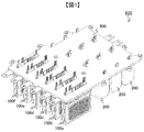
- FIG. 1 is a perspective view of the main circuit unit 900 of the power converter.
- the main circuit unit 900 is a circuit unit that receives DC power from a battery mounted on a vehicle and outputs AC power to a vehicle driving motor.
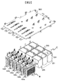
- FIG. 2 is an exploded perspective view of the main circuit unit 900 of the power converter.
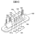
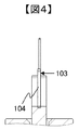
- FIG. 3 is a partial enlarged view of the power terminal 101 and the signal terminal 102 of the power semiconductor module 100a in the range A shown in FIG. 4 is a cross-sectional view of the power semiconductor module 100a as seen from the direction of the arrow on the surface B shown in FIG.
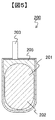
- FIG. 5 is a cross-sectional view of the capacitor module 200 as viewed from the direction of the arrow on plane C in FIG.
- the power semiconductor modules 100a to 100f shown in FIGS. 1 and 2 have inverter circuits that convert DC power into AC power.
- one power semiconductor module 100a constitutes an upper and lower arm circuit for outputting one phase among inverter circuits that output a three-phase alternating current.
- the power semiconductor module 100a is a U-phase upper and lower arm circuit
- the power semiconductor module 100b is a V-phase upper and lower arm circuit
- the power semiconductor module 100c is a W-phase upper and lower arm circuit.
- the power semiconductor modules 100a to 100c constitute a first inverter circuit.
- the power semiconductor module 100d is a U-phase upper and lower arm circuit
- the power semiconductor module 100e is a V-phase upper and lower arm circuit
- the power semiconductor module 100f is a W-phase upper and lower arm circuit.
- the power semiconductor modules 100d to 100f constitute a second inverter circuit. That is, in this embodiment, one inverter is provided with two inverter circuits. These two inverter circuits may drive different motors or may drive one motor.
- the capacitor module 200 shown in FIGS. 2 and 5 includes a capacitor cell 201 such as a film capacitor, and a positive-side capacitor terminal 203 and a negative-side capacitor terminal that electrically connect the capacitor cell 201 and a molded bus bar 500 described later. 204, a capacitor case 202 that houses the capacitor cell 201, and a sealing material 205 filled in the capacitor case 202.
- the power terminal 101 constituting the negative electrode is branched by a first negative power terminal 101a and a second negative power terminal 101c.
- the power terminal 101 constituting the positive electrode is branched by a first positive electrode side power terminal 101b and a second positive electrode side power terminal 101d. Thereby, it is possible to reduce the inductance by avoiding the concentration of the current flowing through the terminal.
- the AC terminal 101e transmits an AC current output to the vehicle drive motor, and is disposed on the side of the first negative power terminal 101a.
- the main surface 103 of the power terminal 101 has an arrangement of a first negative power terminal 101a, a first positive power terminal 101b, a second negative power terminal 101c, and a second positive power terminal 101d. It is a surface that overlaps with the provisional plane 106 substantially parallel to the direction 105.
- the side surface 104 of the power terminal 101 is formed substantially perpendicular to the provisional plane 106. In other words, the side surface 104 of the power terminal 101 overlaps with a plane that intersects the provisional plane 106.
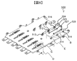
- FIG. 6 is an overall perspective view of the molded bus bar 500.
- FIG. 7 is an exploded perspective view of the molded bus bar 500.
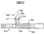
- FIG. 8 is a cross-sectional view of the mold bus bar 500 as seen from the direction of the arrow on the plane D shown in FIG.
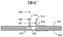
- FIG. 9 is a cross-sectional view of the mold bus bar 500 as seen from the direction of the arrow on the plane E shown in FIG.
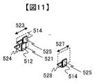
- FIG. 10 is a partially enlarged view of the first terminal 506 of the molded bus bar 500 in the range C shown in FIG. 11 is a partially enlarged view of the second terminal 512 and the third terminal 514 of the molded bus bar 500 in the range B of FIG.
- the molded bus bar 500 includes a negative electrode conductor plate 501, a positive electrode conductor plate 502, a resin material 516, an AC bus bar 504, and an AC bus bar 505.
- the negative electrode conductor plate 501 is disposed in a stacked state with the positive electrode conductor plate 502 so that the main surface of the negative electrode conductor plate 501 faces the main surface of the positive electrode conductor plate 502.
- the AC bus bar 504 shown in FIG. 7 includes an AC bus bar 504a connected to the power semiconductor module 100a, an AC bus bar 504b connected to the power semiconductor module 100b, and an AC bus bar 504c connected to the power semiconductor module 100c. Composed.
- the AC bus bar 505 shown in FIG. 7 includes an AC bus bar 505a connected to the power semiconductor module 100d, an AC bus bar 505b connected to the power semiconductor module 100e, and an AC bus bar 505c connected to the power semiconductor module 100f. Composed.
- the resin material 516 seals a part of each of the positive electrode conductor plate 502, the negative electrode conductor plate 501, the AC bus bar 504, and the AC bus bar 505. Further, the resin material 516 is also inserted between the main surface of the negative electrode conductor plate 501 and the main surface of the positive electrode conductor plate 502 to keep the negative electrode conductor plate 501 and the positive electrode conductor plate 502 insulated.
- the molded bus bar 500 has an AC bus bar 504 and an AC bus bar 505 formed together with the negative electrode conductor plate 501 and the positive electrode conductor plate 502, and is sealed with a resin material 516 to have an integral structure. .
- the molded bus bar 500 is made of high-power wiring sealed with the resin material 516, and the assembly can be expected to improve as a single component.
- the first terminal 506 includes first negative electrode side conductor terminals 507a to 507f, first positive electrode side conductor terminals 508a to 508f, second negative electrode side conductor terminals 509a to 509f, Second positive electrode side conductor terminals 510a to 510f and AC conductor terminals 503a to 503f are configured.
- the first negative electrode side conductor terminals 507a to 507f and the second negative electrode side conductor terminals 509a to 509f are branched from the negative electrode conductor plate 501, respectively, and current is distributed to each.
- the first positive electrode side conductor terminals 508a to 508f and the second positive electrode side conductor terminals 510a to 510f are branched from the positive electrode conductor plate 502, respectively, and current is distributed to each.
- the first negative electrode side conductor terminal 507a is connected to the first negative electrode side power terminal 101a of the power semiconductor module 100a
- the first positive electrode side conductor terminal 508a is connected to the first positive electrode side power terminal 101b of the power semiconductor module 100a
- the second The negative electrode side conductor terminal 509a is connected to the second negative electrode side power terminal 101c of the power semiconductor module 100a
- the second positive electrode side conductor terminal 510a is connected to the second positive electrode side power terminal 101d of the power semiconductor module 100a
- the AC conductor terminal 503a Is connected to the AC terminal 101e of the power semiconductor module 100a.
- the terminals of the other molded bus bars 500 are similarly connected in the same manner as the terminals of the power semiconductor modules 100b to 100f.
- first terminal 506 is arranged so that the second negative electrode side conductor terminals 509a to 509f are arranged between the first positive electrode side conductor terminals 508a to 508f and the second positive electrode side conductor terminals 510a to 510f. Are arranged.
- the first negative electrode side conductor terminal 507a, the first positive electrode side conductor terminal 508a, the second negative electrode side conductor terminal 509a, the second positive electrode side conductor terminal 510a, and the AC conductor terminal 503a are respectively Are formed so that their main surfaces face the same direction.
- the main surface is a surface connected to the terminals of the power semiconductor modules 100b to 100f. That is, the main surface 517 of the first terminal 506 is formed to face in the same direction.
- the side surface 518 of the first terminal 506 is formed so as to cross the main surface 517.
- the second terminal 512 of the present embodiment is configured by nine negative-side conductor terminals connected to the respective negative-side capacitor terminals 204.
- the third terminal 514 of the present embodiment is configured by nine positive electrode side conductor terminals connected to the respective positive electrode side capacitor terminals 203.
- the second terminal 512 and the third terminal 514 are formed such that the main surface 521 of the second terminal 512 and the main surface 525 of the third terminal 514 face the same direction.
- Main surface 521 is connected to negative-side capacitor terminal 204, and main surface 525 is connected to positive-side capacitor terminal 203.
- the side surface 522 of the second terminal 512 is formed so as to cross the main surface 521.
- the side surface 526 of the third terminal 514 is formed so as to cross the main surface 521.
- the third terminal 514 is formed such that the main surface 525 of the third terminal 514 and the main surface 517 of the first terminal 506 face the same direction. Accordingly, the first terminal 506, the second terminal 512, and the third terminal 514 are arranged such that the main surface 517 of the first terminal 506, the main surface 521 of the second terminal 512, and the main surface 525 of the third terminal 514 are in the same direction. Formed.
- the power semiconductor modules 100a to 100f are arranged so that the power terminal 101 faces the main surface 517 of the first terminal 506.
- Capacitor module 200 is arranged such that positive-side capacitor terminal 203 faces main surface 521 of second terminal 512 and negative-side capacitor terminal 204 faces main surface 525 of third terminal 514.
- the main surface 517 of the first terminal 506, the main surface 521 of the second terminal 512, and the third terminal 514 Any one of the main surfaces 525 is in contact with the power terminal 101, the positive-side capacitor terminal 203, or the negative-side capacitor terminal 204, the position of the mold bus bar 500 is corrected around the contact position, and the other terminals can be contacted. .
- the plurality of terminals of the capacitor terminal 204 can reduce the variation in joining to the mold bus bar 500 and facilitate the assembly.
- joining is welding, clip connection, or the like.
- the power terminals 101 of the power semiconductor modules 100a to 100f are the first negative power terminal 101a, the first positive power terminal 101b, the second negative power terminal 101c, and the first power terminal 101c. It is comprised by the 2 positive electrode side power terminal 101d, and the main surface of these terminals has faced the same direction.
- the number of terminals increases, position correction according to each terminal becomes difficult.
- a plurality of first terminals 506 of the molded bus bar 500 are also provided according to the power terminals 101, and the main surface 517 of the first terminals 506 is formed so as to face the same direction, thereby reducing the inductance. As a result, the variation in joining can be reduced and the assembly can be facilitated.
- the main surfaces 517 of the respective terminals constituting the first terminal 506 are the first negative electrode side conductor terminal 507a, the first positive electrode side conductor terminal 508a, and the second negative electrode side conductor terminal 509a. And a surface overlapping the provisional plane 520 substantially parallel to the arrangement direction 519 of the second positive electrode side conductor terminals 510a. As a result, it is possible to further reduce the variation in joining and facilitate assembly while reducing inductance.
- each main surface 521 of the plurality of second terminals 512 is a surface overlapping a provisional plane 524 substantially parallel to the arrangement direction 523 of the plurality of second terminals 512.
- each main surface 525 of the plurality of third terminals 514 is a surface overlapping a provisional plane 528 substantially parallel to the arrangement direction 527 of the plurality of third terminals 514.
- the molded bus bar 500 also holds the AC bus bar 504 and the AC bus bar 505 by the resin material 516.
- the main surfaces of the AC conductor terminals 503a to 503f are also formed to face the same direction as the main surface 517 of the first terminal 506, and are connected to the AC terminal 101e of the power semiconductor module 100a. Thereby, it is possible to further reduce the variation in joining of the main circuit system and facilitate the assembly.
- 529 shown in FIG. 8 is a direction in which the main surface 517 of the first terminal 506 and the main surface 103 of the power terminal 101 of the power semiconductor module 100a are opposed to each other, and when the power semiconductor module 100a and the molded bus bar 500 are connected.
- the mold bus bar 500 is also in the moving direction.
- 9 is a direction in which the main surface 521 of the second terminal 512 and the main surface of the negative-side capacitor terminal 204 face each other, and moves the mold bus bar 500 when the capacitor module 200 and the mold bus bar 500 are connected. It is also a direction.
- SYMBOLS 100a-100f Power semiconductor module, 101 ... Power terminal, 101a ... First negative power terminal, 101b ... First positive power terminal, 101c ... Second negative power terminal, 101d ... Second positive power terminal, 101e DESCRIPTION OF SYMBOLS ... AC terminal, 102 ... Signal terminal, 103 ... Main surface, 104 ... Side surface, 105 ... Arrangement direction, 106 ... Temporary plane, 200 ... Capacitor module, 201 ... Capacitor cell, 202 ... Capacitor case, 203 ... Positive side capacitor terminal, 204 ... Negative side capacitor terminal, 205 ... Sealing material, 500 ... Mold bus bar, 501 ...
Landscapes
- Engineering & Computer Science (AREA)
- Power Engineering (AREA)
- Life Sciences & Earth Sciences (AREA)
- Sustainable Development (AREA)
- Sustainable Energy (AREA)
- Transportation (AREA)
- Mechanical Engineering (AREA)
- Microelectronics & Electronic Packaging (AREA)
- Manufacturing & Machinery (AREA)
- Inverter Devices (AREA)
Abstract
Description
同様に、パワー半導体モジュール100dがU相の上下アーム回路であり、パワー半導体モジュール100eがV相の上下アーム回路であり、パワー半導体モジュール100fがW相の上下アーム回路である。そしてパワー半導体モジュール100dないし100fは、第2インバータ回路を構成する。つまり本実施形態では、一つの電力変換装置に2つのインバータ回路を備える。これら2つのインバータ回路は、それぞれ別々のモータを駆動してもよく、一つのモータを駆動してもよい。
Claims (5)
- パワー端子を有するパワー半導体モジュールと、
前記パワー半導体モジュールに平滑化された電力を供給するコンデンサモジュールと、
前記パワー半導体モジュールと前記コンデンサモジュールとを電気的に接続する導体部が樹脂材により封止されたモールドバスバーと、を備え、
前記コンデンサモジュールは、正極コンデンサ端子及び負極コンデンサ端子を有し、
前記パワー端子と前記正極コンデンサ端子と前記負極コンデンサ端子は、これらの主面が同一方向を向くように形成され、
前記モールドバスバーは、前記パワー端子の主面に接触する第1端子と、前記正極コンデンサ端子の主面と接触する第2端子と、前記負極コンデンサ端子の主面と接触する第3端子を有する電力変換装置。 - 請求項1に記載の電力変換装置であって、
前記パワー端子は、第1正極側パワー端子と、第1負極側パワー端子と、第2正極側パワー端子と、第2負極側パワー端子と、により構成され、かつこれらの主面が同一方向を向くように形成され、
前記第1端子は、前記第1正極側パワー端子と接続される第1正極側導体端子と、前記第1負極側パワー端子と接続される第1負極側導体端子と、前記第2正極側パワー端子と接続される第2正極側導体端子と、前記第2負極側パワー端子と接続される第2負極側導体端子と、により構成され、かつこれらの主面が同一方向を向くように形成される電力変換装置。 - 請求項1に記載の電力変換装置であって、
前記第1端子は、前記第1正極側導体端子の主面と前記第1負極側導体端子の主面と前記第2正極側導体端子の主面と前記第2負極側導体端子の主面が当該第1正極側導体端子と当該第1負極側導体端子と当該第2正極側導体端子と当該第2負極側導体端子の配列方向と平行な仮想平面と重なるように、形成される電力変換装置。 - 請求項1ないし3に記載のいずれかの電力変換装置であって、
前記正極コンデンサ端子は、複数形成され、
さらに前記複数の正極コンデンサ端子は、当該複数の正極コンデンサ端子の主面が当該複数の正極コンデンサ端子の配列方向平行な仮想平面と重なるように、形成される電力変換装置。 - 請求項4に記載の電力変換装置であって、
前記負極コンデンサ端子は、複数形成され、
さらに前記複数の負極コンデンサ端子は、当該複数の負極コンデンサ端子の主面が当該複数の負極コンデンサ端子の配列方向平行な仮想平面と重なるように、形成される電力変換装置。
Priority Applications (4)
| Application Number | Priority Date | Filing Date | Title |
|---|---|---|---|
| DE112016000235.1T DE112016000235T5 (de) | 2015-01-19 | 2016-01-12 | Leistungsumsetzungsvorrichtung |
| CN201680006338.5A CN107210680B (zh) | 2015-01-19 | 2016-01-12 | 电力转换装置 |
| JP2016570580A JP6312228B2 (ja) | 2015-01-19 | 2016-01-12 | 電力変換装置 |
| US15/528,014 US10122313B2 (en) | 2015-01-19 | 2016-01-12 | Power conversion device |
Applications Claiming Priority (2)
| Application Number | Priority Date | Filing Date | Title |
|---|---|---|---|
| JP2015007356 | 2015-01-19 | ||
| JP2015-007356 | 2015-01-19 |
Publications (1)
| Publication Number | Publication Date |
|---|---|
| WO2016117403A1 true WO2016117403A1 (ja) | 2016-07-28 |
Family
ID=56416950
Family Applications (1)
| Application Number | Title | Priority Date | Filing Date |
|---|---|---|---|
| PCT/JP2016/050605 Ceased WO2016117403A1 (ja) | 2015-01-19 | 2016-01-12 | 電力変換装置 |
Country Status (5)
| Country | Link |
|---|---|
| US (1) | US10122313B2 (ja) |
| JP (1) | JP6312228B2 (ja) |
| CN (1) | CN107210680B (ja) |
| DE (1) | DE112016000235T5 (ja) |
| WO (1) | WO2016117403A1 (ja) |
Cited By (1)
| Publication number | Priority date | Publication date | Assignee | Title |
|---|---|---|---|---|
| JP2018046638A (ja) * | 2016-09-14 | 2018-03-22 | 日立オートモティブシステムズ株式会社 | 電力変換装置および電力変換装置の製造方法 |
Families Citing this family (4)
| Publication number | Priority date | Publication date | Assignee | Title |
|---|---|---|---|---|
| JP6398800B2 (ja) * | 2015-03-06 | 2018-10-03 | 株式会社デンソー | 電力変換装置 |
| DE102019100071B4 (de) | 2018-11-26 | 2020-09-10 | Electronicon Kondensatoren Gmbh | Hochleistungskondensatormodul |
| JP7239380B2 (ja) * | 2019-04-16 | 2023-03-14 | 株式会社日立製作所 | 電力変換装置 |
| DE102023112202A1 (de) | 2023-05-10 | 2024-11-14 | Bayerische Motoren Werke Aktiengesellschaft | Wechselrichter |
Citations (2)
| Publication number | Priority date | Publication date | Assignee | Title |
|---|---|---|---|---|
| JP2014050118A (ja) * | 2012-08-29 | 2014-03-17 | Hitachi Ltd | 電気回路装置および電気回路装置の製造方法 |
| JP2014171343A (ja) * | 2013-03-05 | 2014-09-18 | Hitachi Automotive Systems Ltd | 両面冷却型電力変換装置 |
Family Cites Families (10)
| Publication number | Priority date | Publication date | Assignee | Title |
|---|---|---|---|---|
| DE19645636C1 (de) * | 1996-11-06 | 1998-03-12 | Telefunken Microelectron | Leistungsmodul zur Ansteuerung von Elektromotoren |
| JP4305537B2 (ja) * | 2007-03-15 | 2009-07-29 | 株式会社日立製作所 | 電力変換装置 |
| JP5091521B2 (ja) | 2007-03-29 | 2012-12-05 | 三菱重工業株式会社 | 一体型電動圧縮機 |
| JP5227532B2 (ja) * | 2007-04-02 | 2013-07-03 | 日立オートモティブシステムズ株式会社 | インバータ回路用の半導体モジュール |
| JP4533404B2 (ja) * | 2007-05-24 | 2010-09-01 | 日立オートモティブシステムズ株式会社 | エンジン制御装置 |
| JP4580997B2 (ja) * | 2008-03-11 | 2010-11-17 | 日立オートモティブシステムズ株式会社 | 電力変換装置 |
| JP4708459B2 (ja) * | 2008-07-29 | 2011-06-22 | 日立オートモティブシステムズ株式会社 | 電力変換装置 |
| JP4935883B2 (ja) * | 2009-11-27 | 2012-05-23 | 株式会社デンソー | バスバーアッセンブリ |
| JP5879233B2 (ja) * | 2012-08-31 | 2016-03-08 | 日立オートモティブシステムズ株式会社 | パワー半導体モジュール |
| JP5879292B2 (ja) * | 2013-03-28 | 2016-03-08 | 日立オートモティブシステムズ株式会社 | 電力変換装置 |
-
2016
- 2016-01-12 US US15/528,014 patent/US10122313B2/en active Active
- 2016-01-12 WO PCT/JP2016/050605 patent/WO2016117403A1/ja not_active Ceased
- 2016-01-12 JP JP2016570580A patent/JP6312228B2/ja active Active
- 2016-01-12 CN CN201680006338.5A patent/CN107210680B/zh active Active
- 2016-01-12 DE DE112016000235.1T patent/DE112016000235T5/de active Pending
Patent Citations (2)
| Publication number | Priority date | Publication date | Assignee | Title |
|---|---|---|---|---|
| JP2014050118A (ja) * | 2012-08-29 | 2014-03-17 | Hitachi Ltd | 電気回路装置および電気回路装置の製造方法 |
| JP2014171343A (ja) * | 2013-03-05 | 2014-09-18 | Hitachi Automotive Systems Ltd | 両面冷却型電力変換装置 |
Cited By (1)
| Publication number | Priority date | Publication date | Assignee | Title |
|---|---|---|---|---|
| JP2018046638A (ja) * | 2016-09-14 | 2018-03-22 | 日立オートモティブシステムズ株式会社 | 電力変換装置および電力変換装置の製造方法 |
Also Published As
| Publication number | Publication date |
|---|---|
| CN107210680A (zh) | 2017-09-26 |
| CN107210680B (zh) | 2019-10-01 |
| JP6312228B2 (ja) | 2018-04-18 |
| US20170331406A1 (en) | 2017-11-16 |
| US10122313B2 (en) | 2018-11-06 |
| JPWO2016117403A1 (ja) | 2017-08-17 |
| DE112016000235T5 (de) | 2017-09-28 |
Similar Documents
| Publication | Publication Date | Title |
|---|---|---|
| JP4920677B2 (ja) | 電力変換装置およびその組み立て方法 | |
| US9425707B2 (en) | Inverter device capable of appropriately fixing a power module having a switching element and a smoothing capacitor in a limited region | |
| JP6312228B2 (ja) | 電力変換装置 | |
| US20120063187A1 (en) | Inverter device | |
| CN107343387B (zh) | 电力转换装置 | |
| US11424689B2 (en) | Power conversion device | |
| US20180269456A1 (en) | Connector System, Battery Module, Method for Forming a Tap, and Operating Device | |
| WO2023058381A1 (ja) | 電力変換装置 | |
| WO2020012936A1 (ja) | スイッチング素子ユニット及びスイッチング素子モジュール | |
| US10833596B1 (en) | Integrated power unit for a power supply device | |
| WO2019146179A1 (ja) | 電力変換装置および電力変換装置を搭載する電気鉄道車両 | |
| CN113574787A (zh) | 功率转换装置和功率转换装置的制造方法 | |
| CN109729741B (zh) | 半导体装置 | |
| JP7364103B2 (ja) | 電力変換装置 | |
| JP5835167B2 (ja) | パワーモジュール構造 | |
| US20190181128A1 (en) | Power module | |
| JP6862282B2 (ja) | 電力変換装置 | |
| JP7287300B2 (ja) | 電力変換装置 | |
| JP2022130197A (ja) | 電力変換装置、モータモジュール及び車両 | |
| WO2016186087A1 (ja) | コンデンサモジュール | |
| JP2021197829A (ja) | 電力変換装置 | |
| JP7827400B2 (ja) | 電力変換装置 | |
| US20250226762A1 (en) | Output potential switching circuit | |
| JP7205516B2 (ja) | 電力変換装置 | |
| JP7215042B2 (ja) | インバータ |
Legal Events
| Date | Code | Title | Description |
|---|---|---|---|
| 121 | Ep: the epo has been informed by wipo that ep was designated in this application |
Ref document number: 16740010 Country of ref document: EP Kind code of ref document: A1 |
|
| ENP | Entry into the national phase |
Ref document number: 2016570580 Country of ref document: JP Kind code of ref document: A |
|
| WWE | Wipo information: entry into national phase |
Ref document number: 15528014 Country of ref document: US |
|
| WWE | Wipo information: entry into national phase |
Ref document number: 112016000235 Country of ref document: DE |
|
| 122 | Ep: pct application non-entry in european phase |
Ref document number: 16740010 Country of ref document: EP Kind code of ref document: A1 |