WO2016117104A1 - パターン測定装置及び欠陥検査装置 - Google Patents
パターン測定装置及び欠陥検査装置 Download PDFInfo
- Publication number
- WO2016117104A1 WO2016117104A1 PCT/JP2015/051757 JP2015051757W WO2016117104A1 WO 2016117104 A1 WO2016117104 A1 WO 2016117104A1 JP 2015051757 W JP2015051757 W JP 2015051757W WO 2016117104 A1 WO2016117104 A1 WO 2016117104A1
- Authority
- WO
- WIPO (PCT)
- Prior art keywords
- pattern
- image
- sample
- irradiating
- image obtained
- Prior art date
- Legal status (The legal status is an assumption and is not a legal conclusion. Google has not performed a legal analysis and makes no representation as to the accuracy of the status listed.)
- Ceased
Links
Images











Classifications
-
- G—PHYSICS
- G06—COMPUTING OR CALCULATING; COUNTING
- G06T—IMAGE DATA PROCESSING OR GENERATION, IN GENERAL
- G06T7/00—Image analysis
- G06T7/0002—Inspection of images, e.g. flaw detection
- G06T7/0004—Industrial image inspection
-
- G—PHYSICS
- G01—MEASURING; TESTING
- G01B—MEASURING LENGTH, THICKNESS OR SIMILAR LINEAR DIMENSIONS; MEASURING ANGLES; MEASURING AREAS; MEASURING IRREGULARITIES OF SURFACES OR CONTOURS
- G01B15/00—Measuring arrangements characterised by the use of electromagnetic waves or particle radiation, e.g. by the use of microwaves, X-rays, gamma rays or electrons
-
- G—PHYSICS
- G01—MEASURING; TESTING
- G01B—MEASURING LENGTH, THICKNESS OR SIMILAR LINEAR DIMENSIONS; MEASURING ANGLES; MEASURING AREAS; MEASURING IRREGULARITIES OF SURFACES OR CONTOURS
- G01B15/00—Measuring arrangements characterised by the use of electromagnetic waves or particle radiation, e.g. by the use of microwaves, X-rays, gamma rays or electrons
- G01B15/04—Measuring arrangements characterised by the use of electromagnetic waves or particle radiation, e.g. by the use of microwaves, X-rays, gamma rays or electrons for measuring contours or curvatures
-
- G—PHYSICS
- G03—PHOTOGRAPHY; CINEMATOGRAPHY; ANALOGOUS TECHNIQUES USING WAVES OTHER THAN OPTICAL WAVES; ELECTROGRAPHY; HOLOGRAPHY
- G03F—PHOTOMECHANICAL PRODUCTION OF TEXTURED OR PATTERNED SURFACES, e.g. FOR PRINTING, FOR PROCESSING OF SEMICONDUCTOR DEVICES; MATERIALS THEREFOR; ORIGINALS THEREFOR; APPARATUS SPECIALLY ADAPTED THEREFOR
- G03F1/00—Originals for photomechanical production of textured or patterned surfaces, e.g., masks, photo-masks, reticles; Mask blanks or pellicles therefor; Containers specially adapted therefor; Preparation thereof
- G03F1/68—Preparation processes not covered by groups G03F1/20 - G03F1/50
- G03F1/82—Auxiliary processes, e.g. cleaning or inspecting
- G03F1/84—Inspecting
- G03F1/86—Inspecting by charged particle beam [CPB]
-
- G—PHYSICS
- G03—PHOTOGRAPHY; CINEMATOGRAPHY; ANALOGOUS TECHNIQUES USING WAVES OTHER THAN OPTICAL WAVES; ELECTROGRAPHY; HOLOGRAPHY
- G03F—PHOTOMECHANICAL PRODUCTION OF TEXTURED OR PATTERNED SURFACES, e.g. FOR PRINTING, FOR PROCESSING OF SEMICONDUCTOR DEVICES; MATERIALS THEREFOR; ORIGINALS THEREFOR; APPARATUS SPECIALLY ADAPTED THEREFOR
- G03F7/00—Photomechanical, e.g. photolithographic, production of textured or patterned surfaces, e.g. printing surfaces; Materials therefor, e.g. comprising photoresists; Apparatus specially adapted therefor
- G03F7/70—Microphotolithographic exposure; Apparatus therefor
- G03F7/70483—Information management; Active and passive control; Testing; Wafer monitoring, e.g. pattern monitoring
- G03F7/70605—Workpiece metrology
- G03F7/70616—Monitoring the printed patterns
- G03F7/70625—Dimensions, e.g. line width, critical dimension [CD], profile, sidewall angle or edge roughness
-
- H—ELECTRICITY
- H01—ELECTRIC ELEMENTS
- H01J—ELECTRIC DISCHARGE TUBES OR DISCHARGE LAMPS
- H01J37/00—Discharge tubes with provision for introducing objects or material to be exposed to the discharge, e.g. for the purpose of examination or processing thereof
- H01J37/02—Details
- H01J37/22—Optical, image processing or photographic arrangements associated with the tube
-
- H—ELECTRICITY
- H01—ELECTRIC ELEMENTS
- H01J—ELECTRIC DISCHARGE TUBES OR DISCHARGE LAMPS
- H01J37/00—Discharge tubes with provision for introducing objects or material to be exposed to the discharge, e.g. for the purpose of examination or processing thereof
- H01J37/02—Details
- H01J37/22—Optical, image processing or photographic arrangements associated with the tube
- H01J37/222—Image processing arrangements associated with the tube
-
- H—ELECTRICITY
- H01—ELECTRIC ELEMENTS
- H01J—ELECTRIC DISCHARGE TUBES OR DISCHARGE LAMPS
- H01J37/00—Discharge tubes with provision for introducing objects or material to be exposed to the discharge, e.g. for the purpose of examination or processing thereof
- H01J37/26—Electron or ion microscopes; Electron or ion diffraction tubes
- H01J37/28—Electron or ion microscopes; Electron or ion diffraction tubes with scanning beams
-
- G—PHYSICS
- G01—MEASURING; TESTING
- G01B—MEASURING LENGTH, THICKNESS OR SIMILAR LINEAR DIMENSIONS; MEASURING ANGLES; MEASURING AREAS; MEASURING IRREGULARITIES OF SURFACES OR CONTOURS
- G01B2210/00—Aspects not specifically covered by any group under G01B, e.g. of wheel alignment, caliper-like sensors
- G01B2210/56—Measuring geometric parameters of semiconductor structures, e.g. profile, critical dimensions or trench depth
-
- G—PHYSICS
- G06—COMPUTING OR CALCULATING; COUNTING
- G06T—IMAGE DATA PROCESSING OR GENERATION, IN GENERAL
- G06T2207/00—Indexing scheme for image analysis or image enhancement
- G06T2207/10—Image acquisition modality
- G06T2207/10056—Microscopic image
-
- G—PHYSICS
- G06—COMPUTING OR CALCULATING; COUNTING
- G06T—IMAGE DATA PROCESSING OR GENERATION, IN GENERAL
- G06T2207/00—Indexing scheme for image analysis or image enhancement
- G06T2207/30—Subject of image; Context of image processing
- G06T2207/30108—Industrial image inspection
- G06T2207/30148—Semiconductor; IC; Wafer
-
- H—ELECTRICITY
- H01—ELECTRIC ELEMENTS
- H01J—ELECTRIC DISCHARGE TUBES OR DISCHARGE LAMPS
- H01J2237/00—Discharge tubes exposing object to beam, e.g. for analysis treatment, etching, imaging
- H01J2237/245—Detection characterised by the variable being measured
- H01J2237/24592—Inspection and quality control of devices
-
- H—ELECTRICITY
- H01—ELECTRIC ELEMENTS
- H01J—ELECTRIC DISCHARGE TUBES OR DISCHARGE LAMPS
- H01J2237/00—Discharge tubes exposing object to beam, e.g. for analysis treatment, etching, imaging
- H01J2237/26—Electron or ion microscopes
- H01J2237/28—Scanning microscopes
- H01J2237/2813—Scanning microscopes characterised by the application
- H01J2237/2814—Measurement of surface topography
-
- H—ELECTRICITY
- H01—ELECTRIC ELEMENTS
- H01J—ELECTRIC DISCHARGE TUBES OR DISCHARGE LAMPS
- H01J2237/00—Discharge tubes exposing object to beam, e.g. for analysis treatment, etching, imaging
- H01J2237/26—Electron or ion microscopes
- H01J2237/28—Scanning microscopes
- H01J2237/2813—Scanning microscopes characterised by the application
- H01J2237/2817—Pattern inspection
Definitions
- the present invention relates to a pattern measurement device and a computer program for pattern measurement, and more particularly, to a pattern measurement device and a computer program for measuring a pattern evenly arranged on design data.
- Non-Patent Document 1 Non-Patent Document 1
- SAQP method Self Aligned Quadruple Patterning
- a material having high etching resistance is selectively left on the side wall of a pattern formed by lithography, the pattern formed by lithography is deleted, and the remaining side wall is used as a pattern. Therefore, one pattern can be doubled, and if this step is repeated twice, quadrupling is also possible. In other words, the pattern pitch can be reduced to 1/2 or 1/4.
- Non-patent Document 2 a method using a self-guided organization process
- This method uses a material in which two types of polymers called polymer block copolymers are synthesized and block-bonded, and is self-organized using the difference in thermodynamic properties of the two types of polymers. It is the method.
- a plurality of patterns can be formed inside a pattern (guide pattern) formed by lithography, or fine holes can be formed in a self-aligned manner inside large-sized holes.
- Patent Document 1 describes that a plurality of reference lines are superimposed on an outline image obtained based on a scanning electron microscope image of a photomask, and measurement is performed using the reference lines.
- JP 2011-137901 A (corresponding US Patent Publication No. 2012/0290990)
- Non-Patent Documents 1 and 2 a fine pattern exceeding the limit determined by the wavelength of the beam of the projection exposure apparatus can be formed, but the pattern shape formed on the photomask
- Non-Patent Document 1 and Non-Patent Document 2 do not disclose such an evaluation method, and Patent Document 1 does not have a photomask such as DSA, SADP, SAQP, and SAOP (Self-Aligned Octuple Patterning) method.
- DSA DSA, SADP, SAQP, and SAOP (Self-Aligned Octuple Patterning) method.
- a pattern measuring apparatus comprising an arithmetic unit for measuring the dimension of a pattern formed on the sample using data obtained by irradiating the sample with a beam
- the arithmetic device extracts coordinate information of the pattern based on data obtained by irradiating the sample with a beam, and performs measurement when measuring the dimension of the pattern using the coordinate information.
- a pattern measuring device for generating reference data is proposed.
- a defect inspection apparatus comprising an arithmetic unit for detecting a defect on the sample using data obtained by irradiating the sample with a beam, A defect inspection apparatus that detects a defect by comparing a first image obtained by irradiating a beam with a second image obtained by performing autocorrelation processing on the image is proposed.
- a pattern measuring apparatus including an arithmetic unit for measuring a dimension of a pattern formed on the sample using data obtained by irradiating the sample with a beam. Then, the coordinate information of a plurality of first patterns formed on the sample is extracted from the sample data, and the measurement reference data for measuring the second pattern formed between the first patterns is obtained.
- a pattern measuring device to be generated is proposed.
- the figure which shows the grouping method of a measurement pattern The figure which shows an example of the grouped image. The figure which shows the measuring method of the distance between patterns. The figure which shows the grouping method of the distance result between patterns. The figure which shows the method of producing
- New patterning methods such as DSA and SAxP can achieve miniaturization relatively easily, unlike pattern formation methods in general lithography.
- the shape of the pattern changes due to variations in various processes and materials.
- simplification of device patterns is being promoted.
- Gridded Design method as a typical design method. This method is a method of linearizing a device pattern as much as possible and arranging it on an aligned grid, and is suitable for the application of the SADP method or the DSA technique described above. In this way, the microfabrication technology has undergone major changes.
- the embodiments described below are intended to realize high-precision microfabrication and high-performance device manufacturing by accurately measuring and measuring the dimensional variation of these latest pattern forming technologies.
- the edge is recognized from the intensity distribution of secondary electrons and reflected electrons from the edge of the pattern to be measured, the desired edge-to-edge interval is obtained, and the pattern The dimension (CD: Critical dimension), the pitch of the pattern, etc. are obtained.
- CD Critical dimension
- the measurement position select the measurement position by placing a reference line across the edge you want to find and recognizing the edge from the secondary electron intensity distribution, etc. inside the reference line. However, it is necessary to set a reference line at an appropriate position according to the evaluation purpose for the pattern to be evaluated.
- the present embodiment relates to a measurement technique in a manufacturing process for realizing an improvement in device manufacturing yield in the semiconductor manufacturing process.
- the present invention relates to a dimension measuring method when using a so-called self-aligned pattern forming process for multiplying a pattern n times by utilizing process technology and material characteristics, and a measuring apparatus suitable for this.
- a mask pattern is transferred onto a wafer using a reduction projection exposure apparatus.
- the error amount is extremely small and can be ignored. Therefore, the evaluation of the quality of pattern formation is mainly the dimension of the pattern (CD: Critical Dimension).
- Overlay margin management which is an important management item in semiconductor manufacturing, can be performed by managing alignment errors between different layers and pattern dimensions (CD: Critical Dimension).
- a side wall pattern such as an ALD (Atomic Layer Deposition) layer that is self-aligned and formed around the core pattern is used as the pattern. Therefore, the ALD film thickness error and the size of the core resist pattern cause variations in the pattern position.
- ALD Atomic Layer Deposition
- the process position such as ALD film formation causes not only the CD but also the pattern position.
- CD measurement of the line width and interval of the pattern can be performed, but it is not suitable for measurement of the pattern position. That is, there is no pattern that can specify the position in the measurement screen.
- the present embodiment provides a method for evaluating CD variation and position variation collectively.
- the position information of the pattern edge including the pattern position error can be evaluated, the deterioration of the device characteristics due to the overlay error can be prevented in advance, and the device manufacturing yield can be improved.
- the pattern center of gravity or the position of the edge is expressed by a deviation amount with respect to a reference line or a reference point.
- a plurality of reference lines or reference points are arranged on almost the entire area of the CD-SEM measurement screen, and after aligning each pattern edge or pattern centroid with the reference line, the distance between the pattern edge and the reference line or reference point. Measure.
- the reference line or the reference point can be automatically measured from the arrangement of the pattern to be measured, and a method for arranging and a method for inputting and displaying a design value can be selected.
- arranging a measurement pattern for determining the reference pitch and position, obtaining the pattern pitch with this pattern, and obtaining the reference line position are also effective for improving the measurement accuracy.
- a function for calibrating the distortion of the measurement screen can also be added.
- a chip on which a calibration pattern is formed can also be arranged in the measuring device.
- the pattern measurement result for calibration can be applied to screen distortion correction, and a function of arranging a reference line or a reference point according to the screen distortion can be provided.
- an apparatus and a computer program suitable for evaluating a pattern formed by a self-aligned n-fold pattern forming method or a pattern forming method using a self-guided organization material will be described. According to the present embodiment, it is possible to manage the quality of pattern formation and improve the size and position accuracy in the manufacture of advanced devices, which can greatly contribute to the improvement and stabilization of the manufacturing yield.
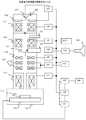
- FIG. 1 is a block diagram showing a schematic configuration of a scanning electron microscope.
- the overall control unit 125 is configured to control the entire apparatus via the electron optical system control device 126 and the stage control device 127 based on the acceleration voltage of electrons input from the user interface 128 by the operator, information on the wafer 111, observation position information, and the like. Control is performed.
- the wafer 111 is fixed on the stage 112 in the sample chamber 113 after passing through the sample exchange chamber via a sample transfer device (not shown).
- the electron optical system control device 126 follows the command from the overall control unit 125, the high voltage control device 115, the first condenser lens control unit 116, the second condenser lens control unit 117, the secondary electron signal amplifier 118, the alignment control unit 119, the deflection.
- the signal control unit 122 and the objective lens control unit 121 are controlled.
- the primary electron beam 103 extracted from the electron source 101 by the extraction electrode 102 is converged by the first condenser lens 104, the second condenser lens 106, and the objective lens 110 and irradiated onto the sample 111.
- the electron beam passes through the aperture 105, and its trajectory is adjusted by the alignment coil 108.
- the deflection coil 109 that receives the signal from the deflection signal control unit 122 via the deflection signal amplifier 120 two-dimensionally on the sample. Scanned.
- the secondary electrons 114 emitted from the sample 111 due to the irradiation of the primary electron beam 103 to the wafer 111 are captured by the secondary electron detector 107, and a secondary electron image is displayed via the secondary electron signal amplifier 118. Used as a luminance signal for the device 124. Since the deflection signal of the secondary electron image display device 124 and the deflection signal of the deflection coil are synchronized, the pattern shape on the wafer 111 is faithfully reproduced on the secondary electron image display device 124.
- the image processor 123 and the secondary electronic image display device 124 may be a general-purpose computer or monitor.
- a storage device 1231 is connected to the image processor 123, and registered information can be read out as necessary.
- the signal output from the secondary electron signal amplifier 118 is AD-converted in the image processor 123 to create digital image data. Further, a secondary electron profile is created from the digital image data.
- ⁇ Select the range to be measured from the created secondary electron profile manually or automatically based on a certain algorithm, and calculate the number of pixels in the selected range.
- the actual dimension on the sample is measured from the actual dimension of the observation area scanned by the primary electron beam 103 and the number of pixels corresponding to the observation area.
- a scanning electron microscope using an electron beam has been described as an example of a charged particle beam apparatus.
- the present invention is not limited to this.
- an ion beam irradiation apparatus using an ion beam may be used.
- an execution subject that executes processing as described later may be referred to as an arithmetic processing unit.
- FIG. 8 is a diagram illustrating an example of a measurement system including a scanning electron microscope.
- This system includes a scanning electron microscope system including an SEM main body 801, a control device 802 for the SEM main body, and an arithmetic processing unit 803.
- the arithmetic processing unit 803 supplies a predetermined control signal to the control unit 802 and performs signal processing of the signal obtained by the SEM main body 801, and the obtained image information and recipe information.
- a memory 805 for storing is incorporated.
- the control device 802 and the arithmetic processing device 803 are described as separate units, but may be an integrated control device.
- Electrons emitted from the sample or generated at the conversion electrode by the beam scanning by the deflector are captured by the detector 806 and converted into a digital signal by the A / D converter built in the control device 802.
- the Image processing according to the purpose is performed by image processing hardware such as a CPU, ASIC, and FPGA incorporated in the arithmetic processing unit 803.
- the arithmetic processing unit 804 includes a profile creation unit 807 that creates a waveform profile based on the signal detected by the detector 806, a first derivative of the signal waveform based on the waveform profile created by the profile creation unit 807, Or the measurement process execution part 808 which measures a pattern dimension based on the signal waveform obtained by quadratic differentiation is included. Further, as will be described later, the measurement processing execution unit 8089 executes a dimension measurement process between the set grid and the center of gravity of the pattern (or the center if the center of gravity coincides with the center). In this case, for example, a difference between coordinate values extracted in units of subpixels and / or a vector thereof may be used as a measurement result.
- the pattern centroid position (from the pattern data obtained based on the design data and simulation data, the pattern edge information included in the SEM image, and the pattern outline data extracted from the pattern edge information ( (Coordinates) is extracted.
- the center of gravity position may be obtained by creating a distance image based on the edge position and detecting the position farthest from the edge in the closed figure.
- the closed figure formed of a polygon may be divided into a plurality of triangles, the area and the center of gravity of the triangle may be integrated, and the center of gravity obtained by dividing by the total area.
- the position between both data is set so that the pattern centroid position obtained based on the design data or the pattern data of the simulation data matches the pattern centroid position obtained based on the edge data of the SEM image. Align.
- both data are set so that the total value of the distances between corresponding centroid positions is minimized. Perform alignment between.
- the alignment pattern selection unit 812 selects a pattern used for alignment (used to extract the position of the center of gravity for alignment) based on a predetermined reference. For example, when evaluating a pattern formed by SAxP, proper alignment cannot be performed if alignment is performed including other patterns. Therefore, in order to automatically select an alignment pattern according to the evaluation purpose, the alignment pattern measurement unit 812 stores the design data storage medium 814 in the design data storage medium 814 based on the measurement purpose and measurement target pattern information input by the input device 815. The region created by the stored SAxP is selectively read out and registered in the alignment processing unit 811 as an alignment image. Alternatively, design data of a pattern area created by SAxP and an area including other areas is read, and a pattern formed by SAxP is selectively registered as an alignment image.
- the arithmetic processing unit 803 executes identification and measurement of an edge or a pattern based on the measurement condition input by the input device 815.
- the arithmetic processing unit 804 includes a design data extraction unit 813 that reads design data from the design data storage medium 814 according to conditions input by the input device 815, and converts vector data into layout data as necessary. Then, the design data extraction unit 813 extracts information necessary for measurement described later from the design data.
- a GUI for displaying images, inspection results, and the like is displayed to the operator.
- the input device 815 also creates an imaging recipe that sets measurement conditions including the coordinates of the electronic device, pattern type, and imaging conditions (optical conditions and stage movement conditions) required for measurement and inspection as imaging recipes. It also functions as a device.
- the input device 815 also has a function of collating the input coordinate information and information on the pattern type with the layer information of the design data and the pattern identification information, and reading out necessary information from the design data storage medium 814. Yes.
- Design data stored in the design data storage medium 814 is expressed in GDS format, OASIS format, etc., and is stored in a predetermined format.
- the design data can be of any type as long as the software that displays the design data can display the format and handle it as graphic data.
- the graphic data is a line segment that has been subjected to a deformation process that approximates the actual pattern by performing an exposure simulation instead of the line segment image information indicating the ideal shape of the pattern formed based on the design data. It may be image information.
- the measurement system illustrated in FIG. 8 includes a photomask measurement SEM 516 for measuring the dimension of the pattern formed on the photomask.
- Photomask measurement results, image data, coordinate information, and the like obtained by the photomask measurement SEM 516 are stored in the memory 805 of the arithmetic processing unit 803 or the like. SEM for photomask measurement
- FIG. 2 is a diagram for explaining a measurement method for evaluating a pattern based on measurement between edges.
- Pattern position information registered in advance from the measurement pattern image 200 or other positions of the measurement pattern 201 on the image obtained by pattern recognition is determined.
- a pattern edge is detected based on the position information, and a pattern CD 203 (pattern width) and an inter-pattern distance 204 are calculated based on the edge information.
- the measurement pattern position on the image can be detected by, for example, template matching between a part of the image cut out by the area designation cursor 205 and another pattern on the image.
- relative measurements such as line width and interval of patterns can be performed, but it is unclear whether each pattern can be formed on target coordinates.
- FIG. 3 shows an example in which a grid is arranged on the SEM image.
- the grid arrangement screen 300 displayed on the secondary electron image display device 124 is an image obtained by overlaying the reference line X301 and the reference line Y302 on the measurement pattern image 200.
- the plurality of reference lines X / Y can be expressed by an arbitrary reference point 303, a pitch X304, and a pitch Y305.
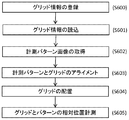
- the measurement process using the grid is divided into a process of registering grid information (S600) and a process of executing grid measurement (S601-S605).
- the pattern centroid position calculation unit 810 of the image processor 123 or the arithmetic processing unit 803 acquires the measurement pattern image (S602), and calculates the pattern centroid 311 from the pattern edge 310 obtained by the means described with reference to FIG.
- There are various methods for calculating the position of the center of gravity For example, after extracting the edge of the pattern, the pattern center of gravity (or center) may be obtained by forming a distance image based on the pattern edge. .
- the distance to the measurement reference point 312 which is one of the intersections of the plurality of reference lines X / Y is calculated, and a deviation amount 313 is output.
- these processes are performed for all the patterns in the screen, and the reference point 303 is aligned so that the total amount of deviation is minimized (S603).
- the field of view includes a pattern other than the pattern formed by SAxP or a pattern other than the pattern formed by self-alignment, these patterns are masked (patterns other than the specific pattern are to be aligned).
- a pattern formed by SAxP or the like can be selectively evaluated.
- this process may not be performed if a reference pattern exists in the measurement screen or outside the screen and is aligned in advance.
- a reference line is placed on the screen (S604), and the relative position between the reference line and the pattern is measured (S605).
- the pattern CD 203 can be output at the same time.
- the grid line information can be registered using an actually acquired SEM image, or can be registered using pattern design data.
- the interval between patterns is determined depending on the type of the polymer block copolymer (in some cases), the polymer block copolymer and grid line information (interval between grid lines) are associated in advance.
- a database to be stored may be prepared, and grid line information may be read based on selection of the polymer block copolymer to be used.
- the interval between grid lines is set to be the same as the interval between patterns on the design data. If the pattern formed by DSA or SAxP is ideally formed according to the design data, it should be formed at the same interval as the grid lines (for example, at equal intervals). Due to the variation (for example, the variation in the film thickness of the layer serving as the mask layer), the interval may vary. As described above, by measuring the dimension between the barycentric positions of a plurality of patterns, it is possible to obtain not only a mere deviation but also information sufficient to grasp the reason for the deviation. This point will be further described later.
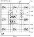
- FIG. 7 is a diagram showing an example in which a grid is arranged on an image on which a pattern formed by the DSA method and a guide pattern for applying the DSA method are displayed.
- the image illustrated in FIG. 7 is acquired at a magnification of 200K (field size 670 nm ⁇ ), and a grid pattern 702 (reference pattern) is superimposed on the acquired image 701.
- the pattern 704 arranged in the guide pattern 703 by the self-guided organization phenomenon can appropriately evaluate the self-guided organization process by appropriately evaluating not only the size but also the formed position.
- the guide pattern 703 is created based on patterning by the reduction projection exposure apparatus, the pattern 704 arranged in the guide pattern 703 may not be formed at an appropriate position depending on the quality of the guide pattern 703. In particular, when the edge of the guide pattern is deformed or the shape is distorted, the pattern may not be arranged at an appropriate position.
- a guide pattern 705 for the reference pattern 706 is patterned together with the guide pattern 703, and a grid is set based on the reference pattern 706.
- eight reference patterns are arranged in the field of view of the electron microscope.
- the interval between the eight reference patterns is set to be an integral multiple of the interval between the DSA patterns arranged in the guide pattern, and on the grid lines arranged evenly between the reference patterns in the design data.
- the grid lines are set so that the pattern formed by self-organization is located.
- the grid pattern can be positioned at an appropriate position by setting an appropriate reference pattern that matches the DSA pattern size.
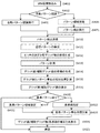
- the SEM image to be measured is read into the image processor 123 and the arithmetic processing unit 803 (S401). At this time, as the SEM image, an image stored in advance in the storage device 1231 or the memory 805 can be used.
- the user selects whether to detect a pattern position by automatic pattern recognition (S402). When automatic is selected, the image processor 123 and the alignment pattern selection unit 812 execute automatic pattern recognition (S403), and calculate pattern detection coordinates (S410).
- the pattern position can be detected by automatically recognizing this repetition period by image processing or the like. In this embodiment, it is left to the user to perform automatic pattern recognition. However, if it can be determined that recognition is possible at this time, it can also be applied during measurement.
- the user designates a pattern area to be measured as in 205 (S404).
- a pattern formed by the DSA method may be selectively extracted from design data or simulation data to form a pattern recognition template (pattern centroid extraction image).
- the image processor 123 and the arithmetic processing unit 803 execute pattern detection (S405), and calculate pattern detection coordinates in the same manner as in automatic pattern recognition (S410). Next, a neighboring pattern having a minimum distance is detected from the detected pattern coordinate group (S411).
- the pitch is determined by calculating the distance that minimizes the distance between neighboring patterns in each of the X and Y directions.
- a method of obtaining from a projected waveform in the X / Y direction or a direction in which a pattern exists by a distance between peaks a method of calculating by a spatial frequency analysis, a method of calculating by an autoregressive model, or the like can be considered.
- the coordinates of the temporary grid line are generated simultaneously with the pitch calculation (S412). Pattern measurement is executed, and the pattern CD and pattern barycentric coordinates are obtained from the edge point group detected during measurement (S413).
- the grid line corrects the temporary grid line using the pattern barycentric coordinates.
- the coordinates of the auxiliary grid lines are also generated from the pattern CD and displayed on the secondary electron image display device 124 (S414).
- a reference pattern area is designated (S421) or a reference line is designated (S422).
- the reference line is designated, the barycentric coordinates of the reference pattern are detected and recalculated. Based on the recalculated information, the grid lines, auxiliary grid lines, and reference lines are corrected and displayed on the secondary electron image display device 124 (S424).
- a method of creating a reference pattern separately from the pattern to be measured and evaluating the positional deviation of the measurement target pattern based on the alignment using the reference pattern explained.
- by performing alignment using a plurality of reference patterns deviations of individual patterns can be averaged, and as a result, highly accurate alignment can be performed.
- measurement reference data such as grid lines is generated in advance, and evaluation based on the data is performed, so that it is possible to properly evaluate the performance of the DSA pattern.
- Such measurement reference data can be generated from, for example, design data (layout data).
- design data layout data
- the guide pattern edge can be generated. It may not be appropriate as a measurement standard for properly evaluating variation caused by failure or failure. In other words, it may be unsuitable for a measurement standard when it is desired to selectively evaluate variations in DSA patterns.
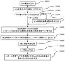
- FIG. 9 is a diagram for explaining the pattern coordinate specifying process.
- FIG. 10 is a conceptual diagram for explaining the processing flow of FIG.
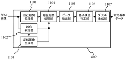
- FIG. 11 is a block diagram showing details of the grid setting unit 809 that generates measurement reference data along the processing steps of FIG.
- the grid setting unit 809 reads the SEM image 5101 (S5001), and the autocorrelation processing unit 1101 creates an autocorrelation map 5102 of the read SEM image (S5002).
- the autocorrelation map obtained here has the highest correlation value at the center coordinates of the map, and the peak interval is approximately equal to the pattern pitch interval in the SEM image. More specifically, a self-image search is performed using the same image as the self-image, and a map in which a portion having a high correlation value is relatively bright is created.
- the unevenness determination unit 1102 determines the unevenness of the pattern of the SEM image (S5003).
- the image can be simply binarized by binarizing Otsu or the like, and the smaller area side can be determined as the pattern portion.
- the inverted image generation unit 1103 generates a luminance inverted image 5103 in which the luminance of the SEM image is inverted (S5004).
- the cross-correlation processing unit 1104 generates a cross-correlation map (S5106) between the autocorrelation map and the SEM image (inversion of luminance when the pattern is concave) (S5005).
- the cross-correlation map can be obtained by a normalized cross-correlation method, a sum of absolute values of luminance value differences, a sum of squares of luminance value differences, or the like.
- the peak coordinates 5105 of the cross-correlation map obtained in this way indicate approximate pattern center coordinates in the SEM image.
- a pattern coordinate map can be generated by detecting the peak position of the cross-correlation map by the peak detection unit 1105 (S5006).
- the lattice structure determination unit 1106 performs determination processing of the lattice structure of the SEM image (S5007).
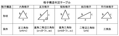
- the peak map where the peak position of the autocorrelation map is detected, or the three points on the pattern coordinate map that are adjacent to each other are selected so as not to be linear, and the area of the triangle formed from the three points is selected to be the smallest.
- the lattice structure is determined based on the shape of a triangle with the vertex at. As shown in FIG.
- a hexagonal lattice is used for equilateral triangles with equal sides
- a tetragonal lattice is used for a right isosceles triangle
- an oblique lattice is used for an isosceles triangle
- a rectangular lattice is used for a right triangle
- the grid generation unit 1107 generates an average grid after the determination process (S5008).
- an average distance between adjacent points in a point sequence arranged in parallel with each side of the triangle is obtained.
- an average distance between adjacent points in a direction parallel to two sides intersecting at right angles of the three points used in lattice determination is calculated. An average grid is created from the average distance thus obtained.
- a grid is created so that the distance between each coordinate of the pattern coordinate map and each point of the average grid is the smallest (S5009).
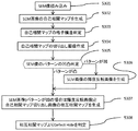
- FIG. 13 an example in which the grid setting unit 809 has a defect detection function will be described.
- the present invention is not limited to this, and a different arithmetic processing device that performs defect detection may be provided.
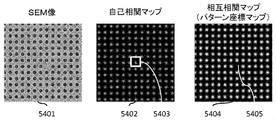
- the grid setting unit 809 reads the SEM image 5401 (S5301), and the autocorrelation processing unit 1101 creates an autocorrelation map 5402 of the SEM image (S5302).
- the lattice structure determination unit 1106 determines the lattice structure of the autocorrelation map (S5303). In the structure determination, the peak position of the autocorrelation map is detected, and the lattice structure determination process described in the first embodiment can be used.
- the image cutout unit 1601 creates a cutout image 5403 of the autocorrelation map. Since the pattern pitch can be calculated from the structure determination, the cutout region may be set to a region that does not overlap the adjacent pattern (for example, a half pitch).
- the unevenness determination unit 1102 performs pattern unevenness determination processing of the SEM image (S5305). If the pattern is concave, the inverted image generation unit 1103 determines the brightness of the SEM image. A reverse image is generated (S5306). In the next processing, the cross-correlation processing unit 1104 creates a cross-correlation map 5404 between the autocorrelation cut-out image and the SEM image (luminance inversion image when the pattern is concave) in order to specify the defect position of the SEM image ( S5307).
- the cross-correlation map can be obtained by a normalized cross-correlation method, a sum of absolute values of luminance value differences, a sum of squares of luminance value differences, or the like.
- the cross-correlation map calculated here there is a peak on the pattern of the SEM image, and no peak appears at the defect position (5405) where the pattern does not exist.
- the position of the defect is specified by detecting the portion not arranged in (S5308).
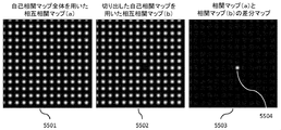
- a difference map 5503 is created based on the difference between the entire autocorrelation map map and the cross correlation map 5501 of the entire SEM image, and the difference between the image obtained by cutting the autocorrelation map and the cross correlation map 5502 of the entire SEM image, and detects the defect position 5504. There is a way to do it. In this method, since the peak 5504 appears at the defect position in the difference map, the defect position can be specified by detecting this peak.
- the shortest distance 5605 between the coordinates 5604 of the pattern coordinate map is calculated, and a range 5606 in which Edge detection is performed is set. If the edge detection range is set to 1 ⁇ 2 of the shortest distance between the cross-correlation peaks, it is possible to set a region not covered by the adjacent pattern. Alternatively, an edge detection range can be set in advance.
- the peak coordinate of the pattern coordinate map generated above is set as the measurement reference position 5604 (Edge detection is not performed at the position determined as Defect), and Edge detection of the pattern is performed within the Edge detection range.
- the Edge detection method can detect Edge by providing a threshold value between the minimum luminance and the maximum luminance obtained from the SEM image.
- the threshold value can be automatically calculated by binarizing Otsu or the like, and the brightness threshold value can be set in advance from the outside.
- a luminance profile is acquired radially from the peak coordinates of the pattern coordinate map, and a position where the differential peak of the luminance profile is maximized can be set as the edge position.
- it is determined whether Edge detection is successful When it is determined by binarization, it can be determined whether or not a closed curve is formed within the edge detection range.
- the brightness profile is acquired in a radial manner and Edge detection is performed, if the differential peak value of the brightness profile exists in each direction within the edge detection range and the edge variation is within a predetermined range, it is determined that Edge detection has been successful. To do.
- Patterns that have succeeded in Edge detection can calculate the center of gravity of each pattern Edge based on the Edge detection result, and calculate the center of gravity variation of the pattern by calculating the distance between the Edge center of each pattern and the corresponding coordinate in the pattern coordinate map. It is.
- FIG. 18 is a flowchart showing a grid generation process.
- the necessary data is the pattern coordinate map 5701 described in the previous embodiment.
- Step 1 at least two pattern coordinates in the direction to be grouped are selected from the pattern coordinate map 5701.
- a coordinate map as illustrated in FIG. 18 is displayed on the display device of the input device 815 illustrated in FIG. 8, and a pattern coordinate 5702 is selected using a pointing device or the like (not shown).
- Step 2 linear approximation is performed from a pattern coordinate point sequence in the vicinity of a straight line passing through the two selected pattern coordinates, and an approximate straight line 5703 is generated. Further, linear approximation is performed for each of the pattern coordinates arranged in parallel with the approximated straight line. Step 2 can also calculate a straight line by Hough transforming the slope of the straight line passing through the two selected pattern coordinates and the pattern coordinate map.
- two pattern coordinates 5704 are selected so as to be different from the direction of the coordinates selected in Step 2.
- Step 4 linear approximation is performed in the same manner as in Step 2. With this method, it is possible to generate grid line 5705 in any direction.
- Step 1 Grid Lines 5801 and 5802 created by using the method described in the above-described embodiment are plotted on the SEM image.
- Step 2 one or more Grid Lines 5803 to be used as a grouping pattern reference are selected.
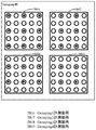
- Step 3 the intersection 5805 of the Grid Line selected in step 1 and step 2 is set as a grouping pattern. If the pattern specified in 5805 is shifted by one pattern period, it can be divided into four groups as shown in a grouping image 5806 illustrated in FIG. Further, as illustrated in FIG. 20, grouping such as grouping images 5807 to 5809 may be performed by setting reference grid lines at other pattern coordinates.
- the shortest distance between Edges between patterns is calculated using Grid Line information set using the method described in the above-described embodiment. Specifically, the distance 5904 between a plurality of adjacent edges located on the Grid Lines 5901 and 5902 is calculated, and the distance 5906 between the combinations of Edges that is the shortest is calculated by comparing the calculated distances 5904. Thus, the distance between patterns can be obtained. Further, not only the Edge distance between patterns but also the center-of-gravity distance between patterns can be calculated by using Grid Line.
- Step 2 For the SEM image 6001, two Grid Lines 6003 serving as a reference are selected in Step 1 using the Grid Line 6002 created using the method described in the above-described embodiment.
- Step 2 one or more grid line 6004 in the same direction as the direction in which the distance is calculated is selected.
- a combination of the inter-pattern distance 6005 to be grouped can be determined.
- the distance 6007 between the patterns in the adjacent array can be designated as the same Grouping.
- the measurement positions can be collectively measured without setting the measurement positions individually for a plurality of patterns and distances between patterns desired to be measured. Setting is possible.
- FIG. 23 is a diagram for explaining a measurement method using a DSA pattern measurement grid.
- FIG. 27 is a diagram for explaining the grid generation unit 1107 illustrated in FIG. 11 in more detail, and illustrates a grid generation unit for generating grid information using DSA pattern information.
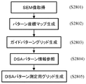
- FIG. 28 is a flowchart showing a process of generating a DSA pattern measurement grid based on SEM image acquisition.
- an electron beam is scanned on a sample on which a guide pattern (guide hole) is formed, and an SEM image of the guide pattern is acquired (step 2801).
- the sample to be scanned with the electron beam is the one before applying the polymer for forming the DSA pattern.
- the average grid generation unit 2701 generates a guide pattern grid 6102 based on the grid generation method described in the above-described embodiments and the like (step 0 in FIG. 23, steps 2802 and 2803 in FIG. 28).
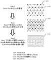
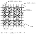
- the DSA grid generation unit 2702 generates a DSA pattern measurement grid 6103 by referring to the DSA pattern information stored in the memory 805 or the like or input from the input device 815 (step 1 in FIG. 23). , Steps 2804 and 2805 in FIG. Since the guide pattern generated by lithography is generated with high accuracy, the grid generated by DSA Hole can be defined in Step 1 with the guide grid as an ideal grid. If the guide pattern is a hexagonal lattice, DSA Hole is generated at the half-pitch location, so the ideal grid is assumed to be on the half-pitch of the guide pattern.
- the guide pattern displayed in the SEM image shows the actual pattern shape, not the ideal shape as in the design data. Since the DSA pattern measurement grid formed by the method as described above indicates the ideal position of the DSA pattern in the actual guide pattern formation state, it is possible to perform an appropriate evaluation according to the result of the guide pattern. Become.
- the barycentric coordinate 6104 of the pattern is obtained from the SEM image of the DSA pattern obtained based on the electron beam scanning on the sample after the DSA pattern is generated, and is compared with the ideal grid to calculate the barycentric deviation from the ideal coordinate. To do. Further, if grouping is performed for each grid line, it is possible to calculate a variation in pattern in each direction, a variation in angle of the pattern arrangement, and the like.
- FIG. 24 illustrates the resist guide pattern resolved after exposure on the substrate or the guide pattern formed by etching and the hole pattern formed by the DSA process.
- the pattern size and pitch (hereinafter referred to as Lo) can be controlled by the guide size and the component ratio of the two types of polymers.
- the ratio of the two types of polymers is 1: 1, and Lo / 2 (approximately Hole diameter) is set to the minimum width of the grid.
- this value indicates the Lo, DSA hole pattern size, and guide pattern. It is possible to set according to the shape. In this example, the generated grid pitch is divided into two.
- FIG. 26 shows an example of the X direction waveform and the Y direction waveform taken out through one DSA hole pattern center.
- the Y waveform near the center of the DSA hole is almost bilaterally symmetric, but the waveform in the X direction is asymmetric, and the signal between the other DSA hole patterns is low. Since it is difficult to determine an edge of a pattern whose signal intensity differs depending on the edge direction, it is difficult to determine an edge with a fixed threshold value. Therefore, the shape evaluation of the Guide pattern and DSA hole obtained by changing the threshold value is performed. Determine the threshold from the value. The measured value of each pattern is calculated from the determined threshold value.
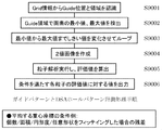
- the guide pattern position and area are recognized from the grid information (S9001).
- the recognition of the area may be a part below a threshold value registered in advance, or may be recognized by template matching.
- a minimum value and a maximum value of the pixel are detected in the recognized Guide region (S9002), and a threshold value is changed from the minimum value to the maximum value (S9003), and a binary image is created (S9004).
- Particle analysis is performed at each threshold value, and evaluation values such as number and area are calculated (S9005). When a plurality of particles are detected, an evaluation value is calculated for all the particles.
- the coordinates of the barycentric coordinates of the particles satisfying the predetermined condition or the input condition or the coordinates of an arbitrary shape are calculated (S9006).
- the value output at this time may be an average value in all cases satisfying the condition, or may be a value obtained by multiplying the weights for a plurality of evaluation values.
- the number of particles, area, circularity, and residual when fitting an arbitrary shape are used.
- the particle area at the threshold that satisfies the condition, the area when fitting an arbitrary shape, especially the average value of the diameter when fitting an ellipse or circle, etc. are output.
- the number of guide patterns is 1 and the number of DSA hole patterns is 2.
- Electron source 102
- Extraction electrode 103
- Primary electron beam (charged particle beam) 104
- First condenser lens 105
- Aperture 106
- Second condenser lens 107
- Secondary electron detector 108
- Alignment coil 109
- Deflection coil 110
- Objective lens 111
- Sample 112 Stage 113
- Sample chamber 114
- Secondary electrons 115
- High voltage controller 116
- First condenser lens controller 117
- Second condenser lens control unit 118
- Secondary electron signal amplifier 119
- Alignment control unit 120
- Deflection signal amplifier 121
- Objective lens control unit 122
- Deflection signal control unit 123
- Image processor 124 Secondary electron image display device
Landscapes
- Physics & Mathematics (AREA)
- General Physics & Mathematics (AREA)
- Engineering & Computer Science (AREA)
- Chemical & Material Sciences (AREA)
- Analytical Chemistry (AREA)
- Computer Vision & Pattern Recognition (AREA)
- Electromagnetism (AREA)
- Quality & Reliability (AREA)
- Theoretical Computer Science (AREA)
- Length-Measuring Devices Using Wave Or Particle Radiation (AREA)
- Testing Or Measuring Of Semiconductors Or The Like (AREA)
Abstract
Description
本実施例の計測では、パターン重心またはエッジの位置を基準線あるいは基準点に対するずれ量で表現する。具体的にはCD-SEM計測画面内のほぼ全域に基準線あるいは基準点を複数配置し、それぞれのパターンエッジあるいはパターン重心と基準線をアライメントした後、パターンエッジと基準線あるいは基準点との距離を計測する。基準線あるいは基準点は、被測定パターンの配列から自動的に計測して、配置する方式と、設計値を入力して表示する方式を選択することができる。
102 引出電極
103 一次電子線(荷電粒子ビーム)
104 第一コンデンサレンズ
105 絞り
106 第二コンデンサレンズ
107 二次電子検出器
108 アライメントコイル
109 偏向コイル
110 対物レンズ
111 試料
112 ステージ
113 試料室
114 二次電子
115 高電圧制御装置
116 第一コンデンサレンズ制御部
117 第二コンデンサレンズ制御部
118 二次電子信号増幅器
119 アライメント制御部
120 偏向信号増幅器
121 対物レンズ制御部
122 偏向信号制御部
123 画像処理プロセッサ
124 二次電子像表示装置
Claims (16)
- 試料にビームを照射することによって得られるデータを用いて、前記試料に形成されたパターンの寸法を測定する演算装置を備えたパターン測定装置において、
前記演算装置は、前記試料にビームを照射することによって得られるデータに基づいて、前記パターンの座標情報を抽出し、当該座標情報を用いて、前記パターンの寸法測定を行う際の測定基準データを生成することを特徴とするパターン測定装置。 - 請求項1において、
前記演算装置は、前記試料にビームを照射することによって得られる第1の画像と、前記試料にビームを照射することによって得られる画像に自己相関処理を施すことによって得られる第2の画像との相関判定に基づいて、前記座標情報を抽出することを特徴とするパターン測定装置。 - 請求項2において、
前記演算装置は、前記第1の画像と第2の画像の相関判定に基づいて、パターン座標マップを生成することを特徴とするパターン測定装置。 - 請求項3において、
前記演算装置は、前記パターン座標マップに含まれる複数の座標を頂点とする形状が所定の形状か否かの判定を行うことを特徴とするパターン測定装置。 - 請求項4において、
前記演算装置は、前記形状判定に応じた方向の線分を持つグリッド線を生成することを特徴とするパターン測定装置。 - 請求項1において、
前記第1の画像は、前記試料にビームを照射することによって得られる画像の輝度を反転させた画像であることを特徴とするパターン測定装置。 - 請求項6において、
前記演算装置は、前記試料上に形成されたパターンが凹パターンである場合に、前記試料にビームを照射することによって得られる画像の輝度を反転させて、前記第1の画像を生成することを特徴とするパターン測定装置。 - 請求項1において、
前記演算装置は、前記抽出された座標情報の配列に応じて、前記パターンの寸法測定を行う際の基準となるグリッド線を生成することを特徴とするパターン測定装置。 - 試料にビームを照射することによって得られるデータを用いて、前記試料上の欠陥を検出する演算装置を備えた欠陥検査装置において、
前記演算装置は、前記試料にビームを照射することによって得られた第1の画像と、当該画像について自己相関処理を施すことによって得られる第2の画像を比較して、欠陥を検出する欠陥検査装置。 - 請求項9において、
前記演算装置は、前記自己相関処理を施すことによって得られる画像の一部を切り出して前記第2の画像を生成し、当該第2の画像と、前記第1の画像の相関判定に基づいて、前記欠陥を検出することを特徴とする欠陥検査装置。 - 請求項10において、
前記演算装置は、前記第1の画像と第2の画像との相関判定に基づいて、相互相関マップを生成することを特徴とする欠陥検査装置。 - 請求項9において、
前記演算装置は、前記試料にビームを照射することによって得られる画像について、自己相関を施すことによって得られた自己相関画像の一部を切り出した切り出し画像と、前記試料にビームを照射することによって得られる画像との相関を求めることによって得られる第1の画像と、前記試料にビームを照射することによって得られる画像について、自己相関を施すことによって得られた自己相関画像と、前記試料にビームを照射することによって得られる画像との相関を求めることによって得られる第2の画像との差分演算に基づいて、前記欠陥を検出することを特徴とする欠陥検査装置。 - 請求項9において、
前記第1の画像は、前記試料にビームを照射することによって得られる画像の輝度を反転させた画像であることを特徴とする欠陥検査装置。 - 請求項13において、
前記演算装置は、前記試料上に形成されたパターンが凹パターンである場合に、前記試料にビームを照射することによって得られる画像の輝度を反転させて、前記第1の画像を生成することを特徴とする欠陥検査装置。 - 試料にビームを照射することによって得られるデータを用いて、前記試料に形成されたパターンの寸法を測定する演算装置を備えたパターン測定装置において、
前記演算装置は、前記試料のデータから前記試料上に形成される複数の第1のパターンの座標情報を抽出し、当該第1のパターン間に形成される第2のパターンを測定する際の測定基準データを生成するパターン測定装置。 - 請求項15において、前記第1のパターンは自己誘導組織化プロセスに用いられるガイドパターンであり、前記第2のパターンは前記自己誘導組織化プロセスによって生成されるパターンであることを特徴とするパターン測定装置。
Priority Applications (5)
| Application Number | Priority Date | Filing Date | Title |
|---|---|---|---|
| PCT/JP2015/051757 WO2016117104A1 (ja) | 2015-01-23 | 2015-01-23 | パターン測定装置及び欠陥検査装置 |
| JP2016570440A JP6423011B2 (ja) | 2015-01-23 | 2015-01-23 | パターン測定装置及び欠陥検査装置 |
| US15/545,067 US10417756B2 (en) | 2015-01-23 | 2015-01-23 | Pattern measurement apparatus and defect inspection apparatus |
| KR1020177018852A KR102012884B1 (ko) | 2015-01-23 | 2015-01-23 | 패턴 측정 장치 및 결함 검사 장치 |
| TW105100805A TWI604177B (zh) | 2015-01-23 | 2016-01-12 | Pattern measuring device and defect inspection device |
Applications Claiming Priority (1)
| Application Number | Priority Date | Filing Date | Title |
|---|---|---|---|
| PCT/JP2015/051757 WO2016117104A1 (ja) | 2015-01-23 | 2015-01-23 | パターン測定装置及び欠陥検査装置 |
Publications (1)
| Publication Number | Publication Date |
|---|---|
| WO2016117104A1 true WO2016117104A1 (ja) | 2016-07-28 |
Family
ID=56416669
Family Applications (1)
| Application Number | Title | Priority Date | Filing Date |
|---|---|---|---|
| PCT/JP2015/051757 Ceased WO2016117104A1 (ja) | 2015-01-23 | 2015-01-23 | パターン測定装置及び欠陥検査装置 |
Country Status (5)
| Country | Link |
|---|---|
| US (1) | US10417756B2 (ja) |
| JP (1) | JP6423011B2 (ja) |
| KR (1) | KR102012884B1 (ja) |
| TW (1) | TWI604177B (ja) |
| WO (1) | WO2016117104A1 (ja) |
Cited By (6)
| Publication number | Priority date | Publication date | Assignee | Title |
|---|---|---|---|---|
| KR20180033367A (ko) * | 2016-09-23 | 2018-04-03 | 삼성전자주식회사 | 패턴 측정 방법 및 그를 포함하는 반도체 소자의 제조 방법 |
| EP3410461A1 (en) * | 2017-05-26 | 2018-12-05 | Jeol Ltd. | Distortion measurement method for electron microscope image, electron microscope, distortion measurement specimen, and method of manufacturing distortion measurement specimen |
| JP2020148655A (ja) * | 2019-03-14 | 2020-09-17 | 株式会社Screenホールディングス | 検査条件作成支援装置、検査条件作成支援方法、検査条件作成支援プログラムおよび記録媒体 |
| JP2020148656A (ja) * | 2019-03-14 | 2020-09-17 | 株式会社Screenホールディングス | 検査条件作成支援装置、検査条件作成支援方法、検査条件作成支援プログラムおよび記録媒体 |
| US10812259B2 (en) | 2017-10-31 | 2020-10-20 | International Business Machines Corporation | Self-assembly based random number generator |
| JP2021505918A (ja) * | 2017-12-11 | 2021-02-18 | ケーエルエー コーポレイション | 走査電子ビーム信号の対称性に基づく重複標的構造のオーバーレイ測定 |
Families Citing this family (11)
| Publication number | Priority date | Publication date | Assignee | Title |
|---|---|---|---|---|
| CN105260733A (zh) * | 2015-09-11 | 2016-01-20 | 北京百度网讯科技有限公司 | 用于处理图像信息的方法和装置 |
| US10163733B2 (en) * | 2016-05-31 | 2018-12-25 | Taiwan Semiconductor Manufacturing Co., Ltd. | Method of extracting defects |
| CN107040725B (zh) * | 2017-05-15 | 2021-04-30 | 惠科股份有限公司 | 一种图像获取装置的坐标校正方法及图像获取装置 |
| JP7155414B2 (ja) * | 2019-05-15 | 2022-10-18 | 株式会社日立ハイテク | 検査装置調整システムおよび検査装置調整方法 |
| EP3862814A1 (en) * | 2020-02-10 | 2021-08-11 | ASML Netherlands B.V. | Multi-step process inspection method |
| CN111275695B (zh) * | 2020-02-10 | 2023-06-02 | 上海集成电路研发中心有限公司 | 一种半导体器件的缺陷检查方法、装置和可读存储介质 |
| US11280749B1 (en) * | 2020-10-23 | 2022-03-22 | Applied Materials Israel Ltd. | Holes tilt angle measurement using FIB diagonal cut |
| JP2022092727A (ja) * | 2020-12-11 | 2022-06-23 | 株式会社日立ハイテク | 観察装置のコンピュータシステムおよび処理方法 |
| JP7718132B2 (ja) * | 2021-07-16 | 2025-08-05 | 日産自動車株式会社 | 自動車製造ラインの塗装欠陥表示方法及びシステム |
| KR102735632B1 (ko) * | 2022-04-15 | 2024-11-29 | 한성대학교 산학협력단 | 파라핀 도포를 최적화하는 방법, 시스템 및 비일시성의 컴퓨터 판독 가능한 기록 매체 |
| US20250265697A1 (en) * | 2024-02-20 | 2025-08-21 | Applied Materials Israel Ltd. | Registration between an inspection image and a design image |
Citations (3)
| Publication number | Priority date | Publication date | Assignee | Title |
|---|---|---|---|---|
| JP2005195361A (ja) * | 2003-12-26 | 2005-07-21 | Hitachi High-Technologies Corp | 走査電子顕微鏡を用いたライン・アンド・スペースパターンの測定方法 |
| JP2007294391A (ja) * | 2006-03-28 | 2007-11-08 | Hitachi High-Technologies Corp | 指定位置特定方法及び指定位置測定装置 |
| JP2013137202A (ja) * | 2011-12-28 | 2013-07-11 | Hitachi High-Technologies Corp | 半導体パターン評価方法および半導体パターン評価装置 |
Family Cites Families (14)
| Publication number | Priority date | Publication date | Assignee | Title |
|---|---|---|---|---|
| JP2000227319A (ja) | 1998-11-30 | 2000-08-15 | Olympus Optical Co Ltd | 欠陥検出装置 |
| EP1061330A1 (en) | 1998-11-30 | 2000-12-20 | Olympus Optical Co., Ltd. | Flaw detector |
| US6326618B1 (en) * | 1999-07-02 | 2001-12-04 | Agere Systems Guardian Corp. | Method of analyzing semiconductor surface with patterned feature using line width metrology |
| JP4035974B2 (ja) | 2001-09-26 | 2008-01-23 | 株式会社日立製作所 | 欠陥観察方法及びその装置 |
| EP1690697A1 (en) * | 2005-02-15 | 2006-08-16 | Alpvision SA | Method to apply an invisible mark on a media |
| US8196216B2 (en) * | 2009-02-27 | 2012-06-05 | State Of Oregon Acting By And Through The State Board Of Higher Education On Behalf Of Portland State University | Systems for assessing and enhancing the performance of scanning probe microscopes by quantifying and enforcing symmetries and periodicities in two dimensions |
| JP5409237B2 (ja) * | 2009-09-28 | 2014-02-05 | キヤノン株式会社 | パターン検出装置、その処理方法及びプログラム |
| JP2011137901A (ja) | 2009-12-28 | 2011-07-14 | Hitachi High-Technologies Corp | パターン計測条件設定装置 |
| JP5049405B2 (ja) * | 2010-03-25 | 2012-10-17 | 三菱レイヨン株式会社 | 陽極酸化アルミナの製造方法、検査装置および検査方法 |
| JP5948074B2 (ja) | 2012-02-13 | 2016-07-06 | 株式会社日立ハイテクノロジーズ | 画像形成装置及び寸法測定装置 |
| WO2015027198A1 (en) * | 2013-08-23 | 2015-02-26 | Kla-Tencor Corporation | Block-to-block reticle inspection |
| FR3010523B1 (fr) * | 2013-09-06 | 2015-09-25 | Safran | Procede de caracterisation d'une piece en materiau composite |
| US10062155B2 (en) * | 2013-11-19 | 2018-08-28 | Lg Display Co., Ltd. | Apparatus and method for detecting defect of image having periodic pattern |
| KR101996492B1 (ko) * | 2014-12-01 | 2019-07-04 | 에이에스엠엘 네델란즈 비.브이. | 리소그래피 제조 프로세스에 관련된 진단 정보를 획득하기 위한 방법 및 장치, 진단 장치를 포함하는 리소그래피 처리 시스템 |
-
2015
- 2015-01-23 JP JP2016570440A patent/JP6423011B2/ja active Active
- 2015-01-23 WO PCT/JP2015/051757 patent/WO2016117104A1/ja not_active Ceased
- 2015-01-23 KR KR1020177018852A patent/KR102012884B1/ko active Active
- 2015-01-23 US US15/545,067 patent/US10417756B2/en active Active
-
2016
- 2016-01-12 TW TW105100805A patent/TWI604177B/zh active
Patent Citations (3)
| Publication number | Priority date | Publication date | Assignee | Title |
|---|---|---|---|---|
| JP2005195361A (ja) * | 2003-12-26 | 2005-07-21 | Hitachi High-Technologies Corp | 走査電子顕微鏡を用いたライン・アンド・スペースパターンの測定方法 |
| JP2007294391A (ja) * | 2006-03-28 | 2007-11-08 | Hitachi High-Technologies Corp | 指定位置特定方法及び指定位置測定装置 |
| JP2013137202A (ja) * | 2011-12-28 | 2013-07-11 | Hitachi High-Technologies Corp | 半導体パターン評価方法および半導体パターン評価装置 |
Cited By (11)
| Publication number | Priority date | Publication date | Assignee | Title |
|---|---|---|---|---|
| KR20180033367A (ko) * | 2016-09-23 | 2018-04-03 | 삼성전자주식회사 | 패턴 측정 방법 및 그를 포함하는 반도체 소자의 제조 방법 |
| KR102773390B1 (ko) * | 2016-09-23 | 2025-02-28 | 삼성전자주식회사 | 패턴 측정 방법 및 그를 포함하는 반도체 소자의 제조 방법 |
| EP3410461A1 (en) * | 2017-05-26 | 2018-12-05 | Jeol Ltd. | Distortion measurement method for electron microscope image, electron microscope, distortion measurement specimen, and method of manufacturing distortion measurement specimen |
| US10541111B2 (en) | 2017-05-26 | 2020-01-21 | Jeol Ltd. | Distortion measurement method for electron microscope image, electron microscope, distortion measurement specimen, and method of manufacturing distortion measurement specimen |
| US10812259B2 (en) | 2017-10-31 | 2020-10-20 | International Business Machines Corporation | Self-assembly based random number generator |
| JP2021505918A (ja) * | 2017-12-11 | 2021-02-18 | ケーエルエー コーポレイション | 走査電子ビーム信号の対称性に基づく重複標的構造のオーバーレイ測定 |
| JP7111826B2 (ja) | 2017-12-11 | 2022-08-02 | ケーエルエー コーポレイション | 走査電子ビーム信号の対称性に基づく重複標的構造のオーバーレイ測定 |
| JP2020148655A (ja) * | 2019-03-14 | 2020-09-17 | 株式会社Screenホールディングス | 検査条件作成支援装置、検査条件作成支援方法、検査条件作成支援プログラムおよび記録媒体 |
| JP2020148656A (ja) * | 2019-03-14 | 2020-09-17 | 株式会社Screenホールディングス | 検査条件作成支援装置、検査条件作成支援方法、検査条件作成支援プログラムおよび記録媒体 |
| JP7152972B2 (ja) | 2019-03-14 | 2022-10-13 | 株式会社Screenホールディングス | 検査条件作成支援装置、検査条件作成支援方法、検査条件作成支援プログラムおよび記録媒体 |
| JP7152973B2 (ja) | 2019-03-14 | 2022-10-13 | 株式会社Screenホールディングス | 検査条件作成支援装置、検査条件作成支援方法、検査条件作成支援プログラムおよび記録媒体 |
Also Published As
| Publication number | Publication date |
|---|---|
| US20180012349A1 (en) | 2018-01-11 |
| TW201640077A (zh) | 2016-11-16 |
| KR20170093931A (ko) | 2017-08-16 |
| TWI604177B (zh) | 2017-11-01 |
| KR102012884B1 (ko) | 2019-08-21 |
| US10417756B2 (en) | 2019-09-17 |
| JPWO2016117104A1 (ja) | 2017-10-26 |
| JP6423011B2 (ja) | 2018-11-14 |
Similar Documents
| Publication | Publication Date | Title |
|---|---|---|
| JP6423011B2 (ja) | パターン測定装置及び欠陥検査装置 | |
| US9702695B2 (en) | Image processing device, charged particle beam device, charged particle beam device adjustment sample, and manufacturing method thereof | |
| TWI579653B (zh) | A pattern measuring device, and a computer program for pattern measurement | |
| US8507856B2 (en) | Pattern measuring method and pattern measuring device | |
| US8311314B2 (en) | Pattern measuring method and pattern measuring device | |
| US10732512B2 (en) | Image processor, method for generating pattern using self-organizing lithographic techniques and computer program | |
| US20110268363A1 (en) | Method for evaluating superimposition of pattern | |
| WO2011030508A1 (ja) | 荷電粒子線装置の信号処理方法、及び信号処理装置 | |
| US20240242334A1 (en) | Method for defect detection in a semiconductor sample in sample images with distortion | |
| KR20110090956A (ko) | 화상 형성 방법, 및 화상 형성 장치 | |
| TWI567789B (zh) | A pattern measuring condition setting means, and a pattern measuring means | |
| JP2011221350A (ja) | マスク検査装置及び画像生成方法 | |
| JP6254856B2 (ja) | 画像補正方法および画像補正プログラム | |
| JP2013178877A (ja) | 荷電粒子線装置 | |
| JP5463334B2 (ja) | パターン測定方法、及びパターン測定装置 |
Legal Events
| Date | Code | Title | Description |
|---|---|---|---|
| 121 | Ep: the epo has been informed by wipo that ep was designated in this application |
Ref document number: 15878797 Country of ref document: EP Kind code of ref document: A1 |
|
| ENP | Entry into the national phase |
Ref document number: 20177018852 Country of ref document: KR Kind code of ref document: A |
|
| ENP | Entry into the national phase |
Ref document number: 2016570440 Country of ref document: JP Kind code of ref document: A |
|
| WWE | Wipo information: entry into national phase |
Ref document number: 15545067 Country of ref document: US |
|
| NENP | Non-entry into the national phase |
Ref country code: DE |
|
| 122 | Ep: pct application non-entry in european phase |
Ref document number: 15878797 Country of ref document: EP Kind code of ref document: A1 |