WO2016106885A1 - 液晶面板和用于固化框胶的方法 - Google Patents
液晶面板和用于固化框胶的方法 Download PDFInfo
- Publication number
- WO2016106885A1 WO2016106885A1 PCT/CN2015/071109 CN2015071109W WO2016106885A1 WO 2016106885 A1 WO2016106885 A1 WO 2016106885A1 CN 2015071109 W CN2015071109 W CN 2015071109W WO 2016106885 A1 WO2016106885 A1 WO 2016106885A1
- Authority
- WO
- WIPO (PCT)
- Prior art keywords
- polarizing plate
- liquid crystal
- crystal panel
- sealant
- color filter
- Prior art date
- Legal status (The legal status is an assumption and is not a legal conclusion. Google has not performed a legal analysis and makes no representation as to the accuracy of the status listed.)
- Ceased
Links
Images



Classifications
-
- G—PHYSICS
- G02—OPTICS
- G02F—OPTICAL DEVICES OR ARRANGEMENTS FOR THE CONTROL OF LIGHT BY MODIFICATION OF THE OPTICAL PROPERTIES OF THE MEDIA OF THE ELEMENTS INVOLVED THEREIN; NON-LINEAR OPTICS; FREQUENCY-CHANGING OF LIGHT; OPTICAL LOGIC ELEMENTS; OPTICAL ANALOGUE/DIGITAL CONVERTERS
- G02F1/00—Devices or arrangements for the control of the intensity, colour, phase, polarisation or direction of light arriving from an independent light source, e.g. switching, gating or modulating; Non-linear optics
- G02F1/01—Devices or arrangements for the control of the intensity, colour, phase, polarisation or direction of light arriving from an independent light source, e.g. switching, gating or modulating; Non-linear optics for the control of the intensity, phase, polarisation or colour
- G02F1/13—Devices or arrangements for the control of the intensity, colour, phase, polarisation or direction of light arriving from an independent light source, e.g. switching, gating or modulating; Non-linear optics for the control of the intensity, phase, polarisation or colour based on liquid crystals, e.g. single liquid crystal display cells
- G02F1/133—Constructional arrangements; Operation of liquid crystal cells; Circuit arrangements
- G02F1/1333—Constructional arrangements; Manufacturing methods
- G02F1/1335—Structural association of cells with optical devices, e.g. polarisers or reflectors
- G02F1/133528—Polarisers
-
- G—PHYSICS
- G02—OPTICS
- G02F—OPTICAL DEVICES OR ARRANGEMENTS FOR THE CONTROL OF LIGHT BY MODIFICATION OF THE OPTICAL PROPERTIES OF THE MEDIA OF THE ELEMENTS INVOLVED THEREIN; NON-LINEAR OPTICS; FREQUENCY-CHANGING OF LIGHT; OPTICAL LOGIC ELEMENTS; OPTICAL ANALOGUE/DIGITAL CONVERTERS
- G02F1/00—Devices or arrangements for the control of the intensity, colour, phase, polarisation or direction of light arriving from an independent light source, e.g. switching, gating or modulating; Non-linear optics
- G02F1/01—Devices or arrangements for the control of the intensity, colour, phase, polarisation or direction of light arriving from an independent light source, e.g. switching, gating or modulating; Non-linear optics for the control of the intensity, phase, polarisation or colour
- G02F1/13—Devices or arrangements for the control of the intensity, colour, phase, polarisation or direction of light arriving from an independent light source, e.g. switching, gating or modulating; Non-linear optics for the control of the intensity, phase, polarisation or colour based on liquid crystals, e.g. single liquid crystal display cells
- G02F1/133—Constructional arrangements; Operation of liquid crystal cells; Circuit arrangements
- G02F1/1333—Constructional arrangements; Manufacturing methods
- G02F1/133308—Support structures for LCD panels, e.g. frames or bezels
-
- G—PHYSICS
- G02—OPTICS
- G02F—OPTICAL DEVICES OR ARRANGEMENTS FOR THE CONTROL OF LIGHT BY MODIFICATION OF THE OPTICAL PROPERTIES OF THE MEDIA OF THE ELEMENTS INVOLVED THEREIN; NON-LINEAR OPTICS; FREQUENCY-CHANGING OF LIGHT; OPTICAL LOGIC ELEMENTS; OPTICAL ANALOGUE/DIGITAL CONVERTERS
- G02F1/00—Devices or arrangements for the control of the intensity, colour, phase, polarisation or direction of light arriving from an independent light source, e.g. switching, gating or modulating; Non-linear optics
- G02F1/01—Devices or arrangements for the control of the intensity, colour, phase, polarisation or direction of light arriving from an independent light source, e.g. switching, gating or modulating; Non-linear optics for the control of the intensity, phase, polarisation or colour
- G02F1/13—Devices or arrangements for the control of the intensity, colour, phase, polarisation or direction of light arriving from an independent light source, e.g. switching, gating or modulating; Non-linear optics for the control of the intensity, phase, polarisation or colour based on liquid crystals, e.g. single liquid crystal display cells
- G02F1/133—Constructional arrangements; Operation of liquid crystal cells; Circuit arrangements
- G02F1/1333—Constructional arrangements; Manufacturing methods
- G02F1/1335—Structural association of cells with optical devices, e.g. polarisers or reflectors
- G02F1/133509—Filters, e.g. light shielding masks
- G02F1/133514—Colour filters
-
- G—PHYSICS
- G02—OPTICS
- G02F—OPTICAL DEVICES OR ARRANGEMENTS FOR THE CONTROL OF LIGHT BY MODIFICATION OF THE OPTICAL PROPERTIES OF THE MEDIA OF THE ELEMENTS INVOLVED THEREIN; NON-LINEAR OPTICS; FREQUENCY-CHANGING OF LIGHT; OPTICAL LOGIC ELEMENTS; OPTICAL ANALOGUE/DIGITAL CONVERTERS
- G02F1/00—Devices or arrangements for the control of the intensity, colour, phase, polarisation or direction of light arriving from an independent light source, e.g. switching, gating or modulating; Non-linear optics
- G02F1/01—Devices or arrangements for the control of the intensity, colour, phase, polarisation or direction of light arriving from an independent light source, e.g. switching, gating or modulating; Non-linear optics for the control of the intensity, phase, polarisation or colour
- G02F1/13—Devices or arrangements for the control of the intensity, colour, phase, polarisation or direction of light arriving from an independent light source, e.g. switching, gating or modulating; Non-linear optics for the control of the intensity, phase, polarisation or colour based on liquid crystals, e.g. single liquid crystal display cells
- G02F1/133—Constructional arrangements; Operation of liquid crystal cells; Circuit arrangements
- G02F1/1333—Constructional arrangements; Manufacturing methods
- G02F1/1339—Gaskets; Spacers; Sealing of cells
-
- G—PHYSICS
- G02—OPTICS
- G02B—OPTICAL ELEMENTS, SYSTEMS OR APPARATUS
- G02B1/00—Optical elements characterised by the material of which they are made; Optical coatings for optical elements
- G02B1/04—Optical elements characterised by the material of which they are made; Optical coatings for optical elements made of organic materials, e.g. plastics
-
- G—PHYSICS
- G02—OPTICS
- G02F—OPTICAL DEVICES OR ARRANGEMENTS FOR THE CONTROL OF LIGHT BY MODIFICATION OF THE OPTICAL PROPERTIES OF THE MEDIA OF THE ELEMENTS INVOLVED THEREIN; NON-LINEAR OPTICS; FREQUENCY-CHANGING OF LIGHT; OPTICAL LOGIC ELEMENTS; OPTICAL ANALOGUE/DIGITAL CONVERTERS
- G02F1/00—Devices or arrangements for the control of the intensity, colour, phase, polarisation or direction of light arriving from an independent light source, e.g. switching, gating or modulating; Non-linear optics
- G02F1/01—Devices or arrangements for the control of the intensity, colour, phase, polarisation or direction of light arriving from an independent light source, e.g. switching, gating or modulating; Non-linear optics for the control of the intensity, phase, polarisation or colour
- G02F1/13—Devices or arrangements for the control of the intensity, colour, phase, polarisation or direction of light arriving from an independent light source, e.g. switching, gating or modulating; Non-linear optics for the control of the intensity, phase, polarisation or colour based on liquid crystals, e.g. single liquid crystal display cells
- G02F1/133—Constructional arrangements; Operation of liquid crystal cells; Circuit arrangements
- G02F1/1333—Constructional arrangements; Manufacturing methods
- G02F1/1335—Structural association of cells with optical devices, e.g. polarisers or reflectors
- G02F1/133509—Filters, e.g. light shielding masks
- G02F1/133512—Light shielding layers, e.g. black matrix
-
- G—PHYSICS
- G02—OPTICS
- G02F—OPTICAL DEVICES OR ARRANGEMENTS FOR THE CONTROL OF LIGHT BY MODIFICATION OF THE OPTICAL PROPERTIES OF THE MEDIA OF THE ELEMENTS INVOLVED THEREIN; NON-LINEAR OPTICS; FREQUENCY-CHANGING OF LIGHT; OPTICAL LOGIC ELEMENTS; OPTICAL ANALOGUE/DIGITAL CONVERTERS
- G02F1/00—Devices or arrangements for the control of the intensity, colour, phase, polarisation or direction of light arriving from an independent light source, e.g. switching, gating or modulating; Non-linear optics
- G02F1/01—Devices or arrangements for the control of the intensity, colour, phase, polarisation or direction of light arriving from an independent light source, e.g. switching, gating or modulating; Non-linear optics for the control of the intensity, phase, polarisation or colour
- G02F1/13—Devices or arrangements for the control of the intensity, colour, phase, polarisation or direction of light arriving from an independent light source, e.g. switching, gating or modulating; Non-linear optics for the control of the intensity, phase, polarisation or colour based on liquid crystals, e.g. single liquid crystal display cells
- G02F1/133—Constructional arrangements; Operation of liquid crystal cells; Circuit arrangements
- G02F1/1333—Constructional arrangements; Manufacturing methods
- G02F1/1335—Structural association of cells with optical devices, e.g. polarisers or reflectors
- G02F1/133528—Polarisers
- G02F1/133531—Polarisers characterised by the arrangement of polariser or analyser axes
-
- G—PHYSICS
- G02—OPTICS
- G02F—OPTICAL DEVICES OR ARRANGEMENTS FOR THE CONTROL OF LIGHT BY MODIFICATION OF THE OPTICAL PROPERTIES OF THE MEDIA OF THE ELEMENTS INVOLVED THEREIN; NON-LINEAR OPTICS; FREQUENCY-CHANGING OF LIGHT; OPTICAL LOGIC ELEMENTS; OPTICAL ANALOGUE/DIGITAL CONVERTERS
- G02F1/00—Devices or arrangements for the control of the intensity, colour, phase, polarisation or direction of light arriving from an independent light source, e.g. switching, gating or modulating; Non-linear optics
- G02F1/01—Devices or arrangements for the control of the intensity, colour, phase, polarisation or direction of light arriving from an independent light source, e.g. switching, gating or modulating; Non-linear optics for the control of the intensity, phase, polarisation or colour
- G02F1/13—Devices or arrangements for the control of the intensity, colour, phase, polarisation or direction of light arriving from an independent light source, e.g. switching, gating or modulating; Non-linear optics for the control of the intensity, phase, polarisation or colour based on liquid crystals, e.g. single liquid crystal display cells
- G02F1/133—Constructional arrangements; Operation of liquid crystal cells; Circuit arrangements
- G02F1/1333—Constructional arrangements; Manufacturing methods
- G02F1/1335—Structural association of cells with optical devices, e.g. polarisers or reflectors
- G02F1/133528—Polarisers
- G02F1/133548—Wire-grid polarisers
Definitions
- the present invention relates to the field of liquid crystal display technologies, and in particular, to a liquid crystal panel and a method for curing the sealant.
- the sealant curing step is an indispensable step in the manufacturing process of a thin film transistor liquid crystal display. Therefore, in the design of a thin film transistor liquid crystal display, factors related to the sealant curing step must be considered.
- the existing frame glue curing methods mainly include two types of conventional methods and slit methods (further described below). However, it is difficult to realize a narrow bezel design by using these two methods to manufacture a liquid crystal panel.
- Figure 1 shows the first type of sealant curing step in the prior art, a "conventional" form of the sealant curing step.
- the liquid crystal panel is designed to include an array substrate 15 , a color filter substrate 11 , and a liquid crystal interlayer sandwiched between the array substrate 15 and the color filter substrate 11 (not shown in the drawing).
- a sealant 16 for encapsulating the liquid crystal is provided on the outer circumference of the liquid crystal interlayer.
- a black matrix (BM) 12 for shielding light is disposed on a side of the color filter substrate 11 facing the liquid crystal interlayer, and a first alignment film 13 is provided at a portion in contact with the liquid crystal.
- BM black matrix
- a metal layer 17 for constituting a thin film transistor or the like is provided on a side of the array substrate 15 facing the liquid crystal interlayer, and a second alignment film 14 is provided at a portion in contact with the liquid crystal.
- BM black matrix
- the ultraviolet light 18 illuminates the sealant 16 to be cured from the side of the color filter substrate 11 and passes through the color filter substrate 11 to be irradiated to the sealant 16. Therefore, In the frame curing step, the light transmittance on the side of the array substrate 15 is not required, and the arrangement of the metal layer 17 is not affected; and at the position corresponding to the sealant 16 on the side of the color filter substrate 11 The black matrix (BM) 12 is dug up.
- the backlight (BL) is normally illuminated from the side of the array substrate 15, there is no light leakage at the edge portion of the liquid crystal panel, and at the edge, except for the position where the sealant 16 is applied.
- BM 12 black matrix
- GIA Gate driver in Array
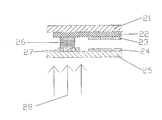
- Fig. 2 shows a second frame seal curing step in the prior art, that is, a "slit method" of the sealant curing step.
- the liquid crystal panel is designed to include an array substrate 25, a color filter substrate 21, and a liquid crystal interlayer sandwiched between the array substrate 25 and the color filter substrate 21 (not shown).
- a sealant 26 for encapsulating the liquid crystal is provided on the outer periphery of the liquid crystal interlayer.
- a black matrix (BM) 22 for shielding light is disposed on a side of the color filter substrate 21 facing the liquid crystal interlayer, and a first alignment film 23 is provided at a portion in contact with the liquid crystal.
- BM black matrix
- a metal layer 27 for forming a thin film transistor or the like is provided on a side of the array substrate 25 facing the liquid crystal interlayer, and a second alignment film 24 is provided at a portion in contact with the liquid crystal.
- a black matrix (BM) 22 is disposed inside the color filter substrate 21 (i.e., the black matrix 22 of the color filter substrate 21 extends all the way to At a position corresponding to the sealant 26, a metal layer 27 having a slit is provided inside the array substrate 25.
- the ultraviolet light 28 is irradiated from the side of the array substrate 25, and at this time, the light transmittance of the metal layer 27 is strictly required.
- the black matrix (BM) 22 on the side of the color filter substrate 21 is entirely flat and extends to a position corresponding to the sealant 26, so that there is no need to worry about light leakage at the edge portion of the liquid crystal panel, and the mechanism design of the display is also performed. There is no need to cover the position of the sealant 26, so the second sealant curing step can be applied to a display with a narrow bezel design.
- the second sealant curing step is required for the light transmittance of the metal layer 27 on the side of the array substrate 25, and is generally greater than 30%.
- the current common practice is to dig the metal layer 27 at the position corresponding to the sealant 26 into a plurality of slit shapes to ensure the transmittance.
- GAA array driver in a Array
- the size of the thin film transistor is large and the light transmittance is low.
- the existing countermeasure is to move the coating position of the sealant 26 outward to avoid the GIA (Gate driver in Array), but it is impossible to adopt a narrow bezel design. Therefore, the first The two types of frame glue curing steps are not applicable to displays having a narrow frame design with a GIA (Gate driver in Array).
- the present invention proposes a liquid crystal panel and a method for curing the sealant, which can be advantageously used for a display having an array substrate row drive circuit using a narrow bezel design.
- a liquid crystal panel includes an array substrate, a color filter substrate, and a liquid crystal interlayer disposed therebetween, and a sealant for encapsulating the sealant is disposed around the liquid crystal interlayer, wherein the color filter substrate is away from the liquid crystal a first polarizing plate is disposed on one side of the interlayer, a second polarizing plate is disposed between the color film substrate and the sealant, and has no black matrix, and a polarization direction of the second polarizing plate is opposite to the first A polarizing plate is perpendicular to each other.
- the sealant is selected as a visible light curing sealant.
- the first polarizing plate when performing the sealant curing step of the liquid crystal panel (according to the conventional processing method in the prior art, the first polarizing plate is not attached to the color film substrate side of the liquid crystal panel at this time),
- the visible light can be irradiated from the side of the color filter substrate of the liquid crystal panel.
- a certain ratio of visible light is transmitted through the second polarizing plate to illuminate the sealant to cure it;
- the liquid crystal panel is normally operated ( At this time, the liquid crystal panel manufacturing process has been completed, so that the first polarizing plate has been attached to the color film substrate side of the liquid crystal panel, and a part of the light from the backlight incident from the array substrate side can pass through the outside of the array substrate.
- the third polarizing plate and the second polarizing plate do not pass through the first polarizing plate (because the polarization direction of the second polarizing plate is perpendicular to the first polarizing plate), so there is no need to worry about the edge of the liquid crystal display during normal use. Light leakage problem.
- the second polarizing plate is located at a position corresponding to the sealant, and the black matrix is located at a position corresponding to the display region.
- the black matrix can perform its normal function, and the second polarizer allows visible light to pass through when the sealant is cured, and the second polarizer cooperates with the first polarizer to block light leakage when the display is normally operated.
- the second polarizing plate is an iodine polyvinyl alcohol type polarizing plate or a dichroic organic dye type polarizing plate.
- the second polarizing plate is a metal wire grid polarizing plate.
- the second polarizer is a metal wire grid polarizer of aluminum or gold.
- the light transmittance of the second polarizing plate is in the range of 30% to 65%.
- the second polarizing plate has a light transmittance of 43%.
- the second polarizer can have The choice of light is transmitted through the direction, and it has a transmittance of 43% when exposed to visible light. With the visible light curing frame glue, the curing effect of the entire liquid crystal panel can be improved.
- the method for curing a sealant according to the present invention comprises at least the following steps:
- a color filter substrate presetting step wherein a second polarizing plate and a black matrix are disposed on a surface of the color filter substrate facing the liquid crystal interlayer such that a position of the second polarizing plate corresponds to a position of the sealant, The position of the black matrix corresponds to the position of the display area,
- a polarizing film for constituting the second polarizing plate is plated on a surface of the color filter substrate facing the liquid crystal interlayer, and then exposed by exposure etching.
- the position of the second polarizing plate corresponds to the position of the sealant, and then the black matrix corresponding to the display area and the color resisting portion are set.
- the second polarizing plate is one of an iodine polyvinyl alcohol type polarizing plate, a dichroic organic dye type polarizing plate, and a metal wire grid polarizing plate, and the light transmittance of the second polarizing plate is located In the range of 30%-65%.
- the liquid crystal panel according to the present invention and the corresponding method for curing the sealant overcome the drawbacks of the prior art by providing the second polarizing plate at an appropriate position, and can be used for a large size.
- the product can also be applied to a liquid crystal panel having an array substrate row driving circuit of a small size, especially a narrow bezel design.
- the liquid crystal panel according to the present invention and the corresponding method for curing the sealant avoid the liquid crystal by making the polarization direction of the second polarizer perpendicular to the polarization direction of the first polarizer located outside the color filter substrate
- the problem of light leakage near the seal at the edge of the screen effectively ensures the quality of the display.
- the constituent materials and light transmittance of the second polarizing plate are further optimized, and these preferred embodiments and frames are further optimized.
- the combination of the properties of the glue itself can obtain a particularly advantageous curing effect of the sealant.
- Figure 1 shows the first type of sealant curing step in the prior art
- Figure 2 shows a second curing step of the sealant in the prior art
- Figure 3 shows a liquid crystal panel according to the present invention
- Figure 4 shows the sealant curing step in the method for curing a sealant in accordance with the present invention.
- FIG. 3 shows a liquid crystal panel in accordance with the present invention.
- a liquid crystal panel according to the present invention includes an array substrate 35, a color filter substrate 31, and a liquid crystal interlayer (not shown) disposed therebetween, and a frame for encapsulating the liquid crystal interlayer is provided around the liquid crystal interlayer Glue 36.
- the first polarizing plate 41 and the third polarizing plate 42 whose polarization directions are perpendicular to each other are respectively disposed on the side of the color filter substrate 31 and the array substrate 35 which are away from the liquid crystal interlayer.
- a second polarizing plate 40 is disposed between the color filter substrate 31 and the sealant 36, and has no black matrix, and the polarization direction of the second polarizing plate 40 is perpendicular to the first polarizing plate 41.
- the first polarizing plate 41 is not attached to the color film substrate 31 side of the liquid crystal panel at this time.
- the visible light 38 can be irradiated from the side of the color filter substrate 31 of the liquid crystal panel.
- the sealant 36 is selected as a visible light curing sealant.
- an alignment film for controlling the liquid crystal pretilt angle is further provided.
- a first alignment film 33 is provided on one surface of the black matrix 32 of the color filter substrate 31 facing the liquid crystal interlayer.
- the first alignment film 33 may be a PI alignment film.
- a second alignment film 34 is provided on one surface of the array substrate 35 facing the liquid crystal interlayer.
- the second alignment film 34 may be a PI alignment film.
- a metal layer 37 for constituting a thin film transistor or the like is further provided on one surface of the array substrate 35 facing the liquid crystal interlayer.
- the first polarizing plate 41 and the third polarizing plate 42 are biased.
- the directions of the vibrations are perpendicular to each other, that is, in the present embodiment, the display adopts a normally black mode.
- the second polarizing plate 40 proposed by the present invention and its working principle that is to say, in other embodiments, the polarization directions of the first polarizing plate 41 and the third polarizing plate 42 may also be uniform, that is, the display may adopt the normally white mode.
- the polarization directions of the second polarizing plate 40 on the inner side of the color filter substrate 31 (the side facing the liquid crystal interlayer) and the first polarizing film 41 on the outer side of the color filter substrate 31 are perpendicular to each other.
- the second polarizing plate 40 is located at a position corresponding to the sealant 36, and the black matrix 32 is located corresponding to the display region. Location.
- the black matrix 32 can perform its conventional function, while the second polarizer 40 allows the visible light 38 to pass through when the sealant is cured, and cooperates with the first polarizer 41 to block light leakage during normal operation of the display.
- the second polarizing plate 40 may be an iodine-based polyvinyl alcohol-type polarizing plate or a dichroic organic dye-based polarizing plate.
- the second polarizer 40 may also be a metal wire grid polarizer, especially a metal wire grid polarizer of aluminum or gold.
- the light transmittance of the second polarizing plate 40 is in the range of 30% to 65%, and in particular, the light transmittance of the second polarizing plate 40 may be 43%. In this way, the second polarizing plate 40 can have a selective transmission direction of light, and has a transmittance of 43% when irradiated with visible light, and can be used to cure the sealant 36 of the entire liquid crystal panel.
- the present invention also proposes a method for curing a sealant, and Figure 4 shows a sealant curing step in a method for curing a sealant according to the present invention.
- the method for curing a sealant according to the present invention comprises at least the following steps:
- a color film substrate presetting step wherein the second polarizing plate 40 and the black matrix 32 are disposed on the surface of the color filter substrate 31 facing the liquid crystal interlayer so that the position of the second polarizing film 40 is opposite to the position of the sealant 36
- the position of the black matrix 32 corresponds to the position of the display area.
- the color film substrate presetting step can be performed in the following specific manner. That is, a polarizing film for constituting the second polarizing plate 40 is plated on the surface of the color filter substrate 31 for facing the liquid crystal interlayer, and then the position of the second polarizing plate 40 is made to correspond to the position of the sealant 36 by exposure etching. Then, the black matrix 32 corresponding to the display area and the color resist portion (not shown) are set.
- the second polarizing plate 40 can be made to be iodine-like by selecting a material for constituting the second polarizing plate 40.
- a material for constituting the second polarizing plate 40 One of a vinyl alcohol type polarizing plate, a dichroic organic dye type polarizing plate, and a metal wire grid polarizing plate, and the light transmittance of the second polarizing plate 40 is in the range of 30% to 65%, preferably 43%. . Because the second polarizing plate 40 has a selective transmission direction of light and a light transmittance of 43% when the visible light is irradiated, and the visible light cures the sealant 36, the curing effect of the sealant of the entire liquid crystal panel can be improved.
- the sealant curing step when the sealant 36 is cured, the visible light 38 is irradiated from the side of the color filter substrate 31 of the liquid crystal panel. At this time, a certain ratio of visible light 38 is transmitted through the second polarizing plate 40, and is irradiated to the sealant 36 to be cured.
- the liquid crystal panel according to the present invention and the corresponding method for curing the sealant overcome the "conventional" sealant curing step (ie, the background by providing the second polarizer 40 at an appropriate position).
- the first sealant curing step in the prior art described in the art) and the "slit method” sealant curing step (ie, the second sealant curing step in the prior art described in the background art) The defect can be used for both large-sized products and liquid crystal panels with a small size, especially a narrow-frame design with a GIA (Gate driver in Array).
- GIA Gate driver in Array
- the liquid crystal panel according to the present invention and the corresponding method for curing the sealant are provided with the second polarizing plate 40 at an appropriate position, and the polarization direction of the second polarizing plate 40 is located outside the color filter substrate 31.
- the polarization directions of the first polarizing plates 41 are perpendicular to each other, which avoids the problem of light leakage near the sealant at the edge of the screen during normal operation of the liquid crystal display, thereby effectively ensuring the quality of the display.
- the constituent materials and light transmittance of the second polarizing plate 40 are further optimized, and these preferred solutions are
- the combination of the properties of the sealant 36 itself results in a particularly advantageous sealant curing effect.
Landscapes
- Physics & Mathematics (AREA)
- Nonlinear Science (AREA)
- General Physics & Mathematics (AREA)
- Optics & Photonics (AREA)
- Mathematical Physics (AREA)
- Chemical & Material Sciences (AREA)
- Crystallography & Structural Chemistry (AREA)
- Liquid Crystal (AREA)
- Devices For Indicating Variable Information By Combining Individual Elements (AREA)
Abstract
一种液晶面板和用于固化框胶的方法,液晶面板包括阵列基板(35)、彩膜基板(31)和设置于二者之间的液晶夹层,在所述液晶夹层周围设置有用于封装其的框胶(36),在所述彩膜基板(31)的远离所述液晶夹层的一侧设置有第一偏振片(41),在所述彩膜基板(31)和所述框胶(36)之间设置有第二偏振片(40)且不具有黑色矩阵。
Description
相关申请的交叉引用
本申请要求享有于2014年12月31日提交的名称为“液晶面板和用于固化框胶的方法”的中国专利申请CN201410851233.2的优先权,该申请的全部内容通过引用并入本文中。
本发明涉及液晶显示技术领域,尤其涉及一种液晶面板和用于固化框胶的方法。
框胶固化步骤是薄膜晶体管液晶显示器的制造过程中不可或缺的步骤。因此,在薄膜晶体管液晶显示器的设计中,必须考虑到与框胶固化步骤相关的因素。现有的框胶固化方式主要包括传统方式和狭缝方式两种(下面将进一步介绍),然而采用这两种方式来制造液晶面板,均难以实现窄边框设计。
图1显示了现有技术中的第一种框胶固化步骤,即“传统方式”的框胶固化步骤。如图1所示,采用这种框胶固化步骤时,液晶面板设计成包括阵列基板15、彩膜基板11以及夹置于阵列基板15和彩膜基板11之间的液晶夹层(图中未显示),而在液晶夹层的外周设置有用于封装液晶的框胶16。其中在彩膜基板11的朝向所述液晶夹层的一侧设置有用于遮光的黑色矩阵(BM)12,同时在与所述液晶相接触的部分设置有第一配向膜13。另一方面,在阵列基板15的朝向所述液晶夹层的一侧设置有用于构成薄膜晶体管等的金属层17,同时在与所述液晶相接触的部分设置有第二配向膜14。从图1中可清楚地看出,在与框胶16相对应的位置处,在彩膜基板11的内侧并未设有黑色矩阵(BM)12(即彩膜基板11的黑色矩阵12并未延伸至与框胶16相对应的位置处),而在阵列基板15的内侧设置有完整的金属层17。当进行“传统方式”的框胶固化步骤时,紫外光18从彩膜基板11侧照射需要固化的框胶16,穿过彩膜基板11而照射到框胶16。因此,
在所述框胶固化步骤中,对阵列基板15一侧的透光率没有要求,进而不影响金属层17的设置;而在彩膜基板11侧的与框胶16对应的位置处,要将黑色矩阵(BM)12挖掉。为了保证正常显示时,当背光源(BL)从阵列基板15侧正常照光时,液晶面板的边缘部分不会出现漏光的情况,在边缘处,除框胶16所涂布的位置以外的地方要全部用黑色矩阵(BM)12遮住,同时框胶16所涂布的位置在机构设计时也会用不透光的结构遮盖起来。这样一来,就要求整个液晶面板的边缘足够大。因此“传统方式”的框胶固化步骤目前主要用于大尺寸的产品,不适用于小尺寸、尤其是采用窄边框设计的具有阵列基板行驱动电路(GIA,Gate driver in Array)的液晶面板。
图2显示了现有技术中的第二种框胶固化步骤,即“狭缝方式”的框胶固化步骤。如图2所示,采用这种框胶固化步骤时,液晶面板设计成包括阵列基板25、彩膜基板21以及夹置于阵列基板25和彩膜基板21之间的液晶夹层(图中未显示),而在液晶夹层的外周设置有用于封装液晶的框胶26。其中在彩膜基板21的朝向所述液晶夹层的一侧设置有用于遮光的黑色矩阵(BM)22,同时在与所述液晶相接触的部分设置有第一配向膜23。另一方面,在阵列基板25的朝向所述液晶夹层的一侧设置有用于形成薄膜晶体管等的金属层27,同时在与所述液晶相接触的部分设置有第二配向膜24。从图2中可清楚地看出,在与框胶26相对应的位置处,在彩膜基板21的内侧设置有黑色矩阵(BM)22(即彩膜基板21的黑色矩阵22一直延伸至与框胶26相对应的位置处),而在阵列基板25的内侧设置有带有狭缝的金属层27。当进行“狭缝方式”的框胶固化步骤时,紫外光28从阵列基板25侧照射,此时对金属层27的透光率有严格的要求。而彩膜基板21侧的黑色矩阵(BM)22是整面的,一直延伸至与框胶26相对应的位置处,这样不必担心液晶面板的边缘部分会有漏光,进行显示器的机构设计时也不需要再去遮掩框胶26的位置处,因此所述第二种框胶固化步骤可以适用于采用窄边框设计的显示器。但是,如前所述,第二种框胶固化步骤对阵列基板25侧的金属层27的透光率是有要求的,一般要大于30%。目前的普遍做法是将与框胶26对应位置处的金属层27挖成多个狭缝状,以保证透过率。但是对于具有阵列基板行驱动电路(GIA,Gate driver in Array)的产品而言,其薄膜晶体管的尺寸很大,透光率很低。现有的应对做法是将框胶26的涂布位置外移,以避开阵列基板行驱动电路(GIA,Gate driver in Array),不过这样做就无法采用窄边框的设计。因此,第
二种框胶固化步骤不适用于采用窄边框设计的具有阵列基板行驱动电路(GIA,Gate driver in Array)的显示器。
发明内容
综上所述,本发明提出了一种液晶面板和用于固化框胶的方法,可有利地用于采用窄边框设计的具有阵列基板行驱动电路的显示器。
根据本发明的液晶面板包括阵列基板、彩膜基板和设置于二者之间的液晶夹层,在所述液晶夹层周围设置有用于封装其的框胶,在所述彩膜基板的远离所述液晶夹层的一侧设置有第一偏振片,在所述彩膜基板和所述框胶之间设置有第二偏振片且不具有黑色矩阵,且所述第二偏振片的偏振方向与所述第一偏振片相互垂直。优选地,框胶选用为可见光固化框胶。
以此方式,一方面,在进行该液晶面板的框胶固化步骤时(根据现有技术中常规的处理方法,此时还未在液晶面板的彩膜基板一侧贴附第一偏振片),可以使得可见光从液晶面板的彩膜基板一侧照射,这时,一定比率的可见光透过第二偏振片,照射到框胶,以使其固化;另一方面,当该液晶面板正常工作时(此时已经完成了液晶面板制造工艺,因此已经在液晶面板的彩膜基板一侧贴附了第一偏振片),从阵列基板侧射入的一部分来自背光源的光线能够通过位于阵列基板外侧的第三偏振片和所述第二偏振片,却不会通过第一偏振片(因为第二偏振片的偏振方向与第一偏振片相互垂直),因此不必担心正常使用时液晶显示器的边缘处的漏光问题。
优选地,在所述彩膜基板的朝向所述液晶夹层的一侧,所述第二偏振片位于与所述框胶相对应的位置处,黑色矩阵位于与显示区域相对应的位置处。如此地,黑色矩阵可以发挥其常规功能,而第二偏振片在固化框胶时允许可见光通过,在显示器正常工作时第二偏振片与第一偏振片配合阻挡漏光。
优选地,所述第二偏振片为碘类聚乙烯醇型偏振片或二色性有机染料型偏振片。
优选地,所述第二偏振片为金属线栅偏振片。优选地,所述第二偏振片为铝或金的金属线栅偏振片。
优选地,所述第二偏振片的透光率位于30%-65%的范围中。
优选地,所述第二偏振片的透光率为43%。以此方式,第二偏振片可以具有
光的选择透过方向,且可见光照射时其具有43%的透过率,搭配可见光固化框胶,可以使整个液晶面板的框胶固化效果良好。
根据本发明的用于固化框胶的方法至少包括如下步骤:
彩膜基板预设步骤,其中在所述彩膜基板的用于面向液晶夹层的表面上设置第二偏振片和黑色矩阵,使得所述第二偏振片的位置与框胶的位置相对应,所述黑色矩阵的位置与显示区域的位置相对应,
框胶固化步骤,其中使得可见光从所述液晶面板的彩膜基板一侧照射。
优选地,在所述彩膜基板预设步骤中,在所述彩膜基板的用于面向液晶夹层的表面上镀上用于构成所述第二偏振片的偏振薄膜,然后通过曝光蚀刻使得所述第二偏振片的位置与框胶的位置相对应,然后再设置与显示区域相对应的黑色矩阵以及色阻部分。
优选地,所述第二偏振片为碘类聚乙烯醇型偏振片、二色性有机染料型偏振片和金属线栅偏振片中的一种,且所述第二偏振片的透光率位于30%-65%的范围中。
以此方式,一方面,根据本发明的液晶面板以及相应的用于固化框胶的方法通过在适当的位置处设置第二偏振片,克服了现有技术的缺陷,既可以用于大尺寸的产品,也可以适用于小尺寸、尤其是采用窄边框设计的具有阵列基板行驱动电路的液晶面板。
另一方面,根据本发明的液晶面板以及相应的用于固化框胶的方法通过使得第二偏振片的偏振方向与位于彩膜基板外侧的第一偏振片的偏振方向相互垂直,避免了在液晶显示器正常工作时,屏幕边缘处框胶附近漏光的问题,有效保障了显示器的质量。
另外,在根据本发明的液晶面板以及相应的用于固化框胶的方法的进一步的优选方案中,对第二偏振片的构成材料和透光率进行了进一步的优化,这些优选的方案与框胶自身的性质配合,可以得到尤其有利的框胶固化效果。
上述技术特征可以各种适合的方式组合或由等效的技术特征来替代,只要能够达到本发明的目的。
在下文中将基于实施例并参考附图来对本发明进行更详细的描述。其中:
图1显示了现有技术中的第一种框胶固化步骤;
图2显示了现有技术中的第二种框胶固化步骤;
图3显示了根据本发明的液晶面板;
图4显示了根据本发明的用于固化框胶的方法中的框胶固化步骤。
在附图中,相同的部件使用相同的附图标记。附图并未按照实际的比例。
下面将结合附图对本发明作进一步说明。
图3显示了根据本发明的液晶面板。参照图3,根据本发明的液晶面板包括阵列基板35、彩膜基板31和设置于二者之间的液晶夹层(图中未示出),在所述液晶夹层周围设置有用于封装其的框胶36。在彩膜基板31和阵列基板35的远离液晶夹层的一侧分别设置有偏振方向相互垂直的第一偏振片41和第三偏振片42。在彩膜基板31和框胶36之间设置有第二偏振片40,且不具有黑色矩阵,且第二偏振片40的偏振方向与第一偏振片41相互垂直。以此方式,一方面,在进行该液晶面板的框胶固化步骤时(根据现有技术中常规的处理方法,此时还未在液晶面板的彩膜基板31一侧贴附第一偏振片41),可以使得可见光38从液晶面板的彩膜基板31一侧照射,这时,一定比率的可见光38透过第二偏振片40,照射到框胶36,以使其固化;另一方面,当该液晶面板正常工作时(此时已经完成了液晶面板制造工艺,因此已经在液晶面板的彩膜基板一侧贴附了第一偏振片41),从阵列基板35侧射入的一部分来自背光源的光线能够通过位于阵列基板35外侧的第三偏振片42和第二偏振片40,却不会通过第一偏振片41(因为第二偏振片40的偏振方向与第一偏振片41相互垂直),因此不必担心正常使用时液晶显示器的边缘处的漏光问题。优选地,框胶36选用为可见光固化框胶。
如图3所示,为了控制位于阵列基板35和彩膜基板31之间的液晶夹层的液晶预倾角,还设置有用于控制液晶预倾角的配向膜。具体地,在彩膜基板31的黑色矩阵32的面向液晶夹层的一面设置有第一配向膜33。具体地,第一配向膜33可以为PI配向膜。类似地,在阵列基板35的面向液晶夹层的一面设置有第二配向膜34。具体地,第二配向膜34可以为PI配向膜。在阵列基板35的面向液晶夹层的一面还设置有用于构成薄膜晶体管等的金属层37。
另外,需要注意的是,在本实施例中,第一偏振片41和第三偏振片42的偏
振方向相互垂直,即在本实施例中显示器采用常黑模式。然而,可以理解,这一点与本发明所提出的第二偏振片40与其工作原理没有任何关系。也就是说,在其它的实施例中,第一偏振片41和第三偏振片42的偏振方向也可以是一致的,即显示器完全可以采用常白模式。就这一点而言,只要保证位于彩膜基板31的内侧(朝向液晶夹层的一侧)上的第二偏振片40与位于彩膜基板31的外侧的第一偏振片41的偏振方向相互垂直即可,因为这样在显示器正常工作时,不会在显示屏幕的边缘处(即与液晶面板的框胶36相对应的位置处)产生漏光,能够在保证显示器的正常显示品质的基础上,优化框胶固化效果。
再次参照图3,可以清楚地看出,在彩膜基板31的朝向液晶夹层的一侧,第二偏振片40位于与框胶36相对应的位置处,黑色矩阵32位于与显示区域相对应的位置处。如此地,黑色矩阵32可以发挥其常规功能,而第二偏振片40在固化框胶时允许可见光38通过,在显示器正常工作时与第一偏振片41配合阻挡漏光。
具体地,第二偏振片40可以为碘类聚乙烯醇型偏振片或二色性有机染料型偏振片。然而,在其它的实施方式中,第二偏振片40也可以为金属线栅偏振片,尤其是铝或金的金属线栅偏振片。第二偏振片40的透光率位于30%-65%的范围中,尤其是,第二偏振片40的透光率可为43%。以此方式,第二偏振片40可以具有光的选择透过方向,且可见光照射时其具有43%的透过率,搭配可见光固化框胶36,可以使整个液晶面板的框胶固化效果良好。
本发明还提出了一种用于固化框胶的方法,图4显示了根据本发明的用于固化框胶的方法中的框胶固化步骤。
根据本发明的用于固化框胶的方法至少包括如下步骤:
a.彩膜基板预设步骤:其中在彩膜基板31的用于面向液晶夹层的表面上设置第二偏振片40和黑色矩阵32,使得第二偏振片40的位置与框胶36的位置相对应,而黑色矩阵32的位置与显示区域的位置相对应。
进一步地,可通过如下具体方式来进行上述彩膜基板预设步骤。即,在彩膜基板31的用于面向液晶夹层的表面上镀上用于构成第二偏振片40的偏振薄膜,然后通过曝光蚀刻使得第二偏振片40的位置与框胶36的位置相对应,然后再设置与显示区域相对应的黑色矩阵32以及色阻部分(图中未显示)。
通过选择用于构成第二偏振片40的材料,可以使得第二偏振片40为碘类聚
乙烯醇型偏振片、二色性有机染料型偏振片和金属线栅偏振片中的一种,且使得第二偏振片40的透光率位于30%-65%的范围中,优选为43%。因为这样可使得第二偏振片40具有光的选择透过方向,同时可见光照射时其具有43%的光透过率,搭配可见光固化框胶36,可以使整个液晶面板的框胶固化效果良好。
b.框胶固化步骤:在对框胶36进行固化时,使得可见光38从液晶面板的彩膜基板31一侧照射。此时,一定比率的可见光38透过第二偏振片40,照射到框胶36,以使其固化。
以此方式,一方面,根据本发明的液晶面板以及相应的用于固化框胶的方法通过在适当的位置处设置第二偏振片40,克服了“传统方式”的框胶固化步骤(即背景技术中所介绍的现有技术中的第一种框胶固化步骤)和“狭缝方式”的框胶固化步骤(即背景技术中所介绍的现有技术中的第二种框胶固化步骤)的缺陷,既可以用于大尺寸的产品,也可以适用于小尺寸、尤其是采用窄边框设计的具有阵列基板行驱动电路(GIA,Gate driver in Array)的液晶面板。
另一方面,根据本发明的液晶面板以及相应的用于固化框胶的方法通过在适当的位置处设置第二偏振片40,并且使得第二偏振片40的偏振方向与位于彩膜基板31外侧的第一偏振片41的偏振方向相互垂直,避免了在液晶显示器正常工作时,屏幕边缘处框胶附近漏光的问题,有效保障了显示器的质量。
另外,在根据本发明的液晶面板以及相应的用于固化框胶的方法的进一步的优选方案中,对第二偏振片40的构成材料和透光率进行了进一步的优化,这些优选的方案与框胶36自身的性质配合,可以得到尤其有利的框胶固化效果。
虽然在本文中参照了特定的实施方式来描述本发明,但是应该理解的是,这些实施例仅仅是本发明的原理和应用的示例。因此应该理解的是,可以对示例性的实施例进行许多修改,并且可以设计出其他的布置,只要不偏离所附权利要求所限定的本发明的精神和范围。应该理解的是,可以通过不同于原始权利要求所描述的方式来结合不同的从属权利要求和本文中所述的特征。还可以理解的是,结合单独实施例所描述的特征可以使用在其他所述实施例中。
Claims (14)
- 液晶面板,所述液晶面板包括阵列基板、彩膜基板和设置于二者之间的液晶夹层,在所述液晶夹层周围设置有用于封装其的框胶,其中,在所述彩膜基板的远离所述液晶夹层的一侧设置有第一偏振片,在所述彩膜基板和所述框胶之间设置有第二偏振片且不具有黑色矩阵,且所述第二偏振片的偏振方向与所述第一偏振片相互垂直。
- 根据权利要求1所述的液晶面板,其中,在所述彩膜基板的朝向所述液晶夹层的一侧,所述第二偏振片位于与所述框胶相对应的位置处,黑色矩阵位于与显示区域相对应的位置处。
- 根据权利要求1所述的液晶面板,其中,所述第二偏振片为碘类聚乙烯醇型偏振片或二色性有机染料型偏振片。
- 根据权利要求1所述的液晶面板,其中,所述第二偏振片为金属线栅偏振片。
- 根据权利要求4所述的液晶面板,其中,所述第二偏振片为铝或金的金属线栅偏振片。
- 根据权利要求1所述的液晶面板,其中,所述第二偏振片的透光率位于30%-65%的范围中。
- 根据权利要求6所述的液晶面板,其中,所述第二偏振片的透光率为43%。
- 根据权利要求2所述的液晶面板,其中,所述第二偏振片的透光率位于30%-65%的范围中。
- 根据权利要求3所述的液晶面板,其中,所述第二偏振片的透光率位于30%-65%的范围中。
- 根据权利要求4所述的液晶面板,其中,所述第二偏振片的透光率位于30%-65%的范围中。
- 根据权利要求5所述的液晶面板,其中,所述第二偏振片的透光率位于30%-65%的范围中。
- 用于固化框胶的方法,其中,至少包括如下步骤:彩膜基板预设步骤,其中在所述彩膜基板的用于面向液晶夹层的表面上设置第二偏振片和黑色矩阵,使得所述第二偏振片的位置与框胶的位置相对应,所述 黑色矩阵的位置与显示区域的位置相对应,框胶固化步骤,其中使得可见光从所述液晶面板的彩膜基板一侧照射。
- 根据权利要求12所述的方法,其中,在所述彩膜基板预设步骤中,在所述彩膜基板的用于面向液晶夹层的表面上镀上用于构成所述第二偏振片的偏振薄膜,然后通过曝光蚀刻使得所述第二偏振片的位置与框胶的位置相对应,然后再设置与显示区域相对应的黑色矩阵以及色阻部分。
- 根据权利要求13所述的方法,其中,所述第二偏振片为碘类聚乙烯醇型偏振片、二色性有机染料型偏振片和金属线栅偏振片中的一种,且所述第二偏振片的透光率位于30%-65%的范围中。
Priority Applications (1)
| Application Number | Priority Date | Filing Date | Title |
|---|---|---|---|
| US14/417,812 US9952464B2 (en) | 2014-12-31 | 2015-01-20 | Liquid crystal display panel and method for curing frame glue |
Applications Claiming Priority (2)
| Application Number | Priority Date | Filing Date | Title |
|---|---|---|---|
| CN201410851233.2A CN104503152A (zh) | 2014-12-31 | 2014-12-31 | 液晶面板和用于固化框胶的方法 |
| CN201410851233.2 | 2014-12-31 |
Publications (1)
| Publication Number | Publication Date |
|---|---|
| WO2016106885A1 true WO2016106885A1 (zh) | 2016-07-07 |
Family
ID=52944557
Family Applications (1)
| Application Number | Title | Priority Date | Filing Date |
|---|---|---|---|
| PCT/CN2015/071109 Ceased WO2016106885A1 (zh) | 2014-12-31 | 2015-01-20 | 液晶面板和用于固化框胶的方法 |
Country Status (3)
| Country | Link |
|---|---|
| US (1) | US9952464B2 (zh) |
| CN (1) | CN104503152A (zh) |
| WO (1) | WO2016106885A1 (zh) |
Families Citing this family (13)
| Publication number | Priority date | Publication date | Assignee | Title |
|---|---|---|---|---|
| CN104615306B (zh) * | 2015-02-13 | 2017-10-31 | 厦门天马微电子有限公司 | 一种触摸屏及其制造方法 |
| CN104765192A (zh) * | 2015-04-30 | 2015-07-08 | 京东方科技集团股份有限公司 | 一种液晶显示面板及其制作方法、显示装置 |
| CN106200033B (zh) * | 2015-05-06 | 2019-10-11 | 凌巨科技股份有限公司 | 窄边框显示器 |
| CN105093626B (zh) * | 2015-08-13 | 2018-04-20 | 京东方科技集团股份有限公司 | 显示面板及其制造方法 |
| CN105116629A (zh) * | 2015-09-16 | 2015-12-02 | 京东方科技集团股份有限公司 | 一种封框胶组合物、显示面板及其制备方法、显示装置 |
| KR102581143B1 (ko) * | 2016-08-18 | 2023-09-21 | 삼성디스플레이 주식회사 | 표시 장치 |
| CN106292046A (zh) * | 2016-08-19 | 2017-01-04 | 京东方科技集团股份有限公司 | 一种显示面板及制作方法 |
| CN106773275B (zh) * | 2017-03-15 | 2020-06-02 | 厦门天马微电子有限公司 | 显示面板及其制备方法、显示装置 |
| CN109426025A (zh) * | 2017-08-31 | 2019-03-05 | 京东方科技集团股份有限公司 | 一种液晶显示面板、其制备方法、彩膜基板及显示装置 |
| CN108873493B (zh) * | 2018-06-28 | 2021-05-04 | 上海天马微电子有限公司 | 液晶显示面板、装置以及液晶显示面板的框胶固化方法 |
| CN110596937A (zh) * | 2019-08-13 | 2019-12-20 | 昆山龙腾光电有限公司 | 彩膜基板、显示面板及显示装置 |
| US11829026B2 (en) | 2019-09-26 | 2023-11-28 | Boe Technology Group Co., Ltd. | Display panel, driving method thereof and display device |
| CN115236894B (zh) * | 2022-07-28 | 2023-12-26 | 福州京东方光电科技有限公司 | 显示面板、其制作方法及显示装置 |
Citations (6)
| Publication number | Priority date | Publication date | Assignee | Title |
|---|---|---|---|---|
| US20110194062A1 (en) * | 2010-02-11 | 2011-08-11 | Samsung Mobile Display Co., Ltd. | Liquid crystal display device |
| CN102662275A (zh) * | 2012-04-27 | 2012-09-12 | 深圳市华星光电技术有限公司 | 液晶显示模组及液晶显示装置 |
| CN102929057A (zh) * | 2012-11-09 | 2013-02-13 | 京东方科技集团股份有限公司 | 一种液晶显示面板及其制造方法和液晶显示装置 |
| CN103018968A (zh) * | 2012-12-12 | 2013-04-03 | 京东方科技集团股份有限公司 | 一种封框胶的固化方法 |
| CN103257483A (zh) * | 2013-05-23 | 2013-08-21 | 深圳市华星光电技术有限公司 | 液晶显示设备的制作方法 |
| CN103409084A (zh) * | 2013-08-14 | 2013-11-27 | 京东方科技集团股份有限公司 | 封框胶组合物、显示器件及检测方法 |
Family Cites Families (10)
| Publication number | Priority date | Publication date | Assignee | Title |
|---|---|---|---|---|
| CN100403134C (zh) * | 2002-08-02 | 2008-07-16 | 奇美电子股份有限公司 | 液晶显示器 |
| JP2007114704A (ja) * | 2005-10-24 | 2007-05-10 | Nec Lcd Technologies Ltd | 液晶表示装置およびその製造方法 |
| US20070229733A1 (en) * | 2006-04-03 | 2007-10-04 | Duck-Jong Suh | Liquid crystal display, panel for the same and method of manufacture |
| KR20070099399A (ko) * | 2006-04-03 | 2007-10-09 | 삼성전자주식회사 | 액정 표시 장치, 그에 사용되는 표시판 및 그 제조 방법 |
| JP4708287B2 (ja) * | 2006-08-25 | 2011-06-22 | 富士フイルム株式会社 | 光学フィルムの製造方法、光学フィルム、偏光板、転写材料、液晶表示装置、及び偏光紫外線露光装置 |
| JP2008129379A (ja) * | 2006-11-22 | 2008-06-05 | Victor Co Of Japan Ltd | 液晶表示素子 |
| JP5094255B2 (ja) * | 2007-07-19 | 2012-12-12 | 株式会社ジャパンディスプレイイースト | 液晶表示装置、及びその製造方法 |
| CN100573204C (zh) * | 2008-04-30 | 2009-12-23 | 京东方科技集团股份有限公司 | 偏振片制造方法 |
| CN102799018A (zh) * | 2012-08-09 | 2012-11-28 | 深圳市华星光电技术有限公司 | 液晶显示面板及其制造方法 |
| CN103353692B (zh) * | 2013-06-28 | 2016-06-15 | 京东方科技集团股份有限公司 | 一种显示面板及其制备方法和显示装置 |
-
2014
- 2014-12-31 CN CN201410851233.2A patent/CN104503152A/zh active Pending
-
2015
- 2015-01-20 US US14/417,812 patent/US9952464B2/en active Active
- 2015-01-20 WO PCT/CN2015/071109 patent/WO2016106885A1/zh not_active Ceased
Patent Citations (6)
| Publication number | Priority date | Publication date | Assignee | Title |
|---|---|---|---|---|
| US20110194062A1 (en) * | 2010-02-11 | 2011-08-11 | Samsung Mobile Display Co., Ltd. | Liquid crystal display device |
| CN102662275A (zh) * | 2012-04-27 | 2012-09-12 | 深圳市华星光电技术有限公司 | 液晶显示模组及液晶显示装置 |
| CN102929057A (zh) * | 2012-11-09 | 2013-02-13 | 京东方科技集团股份有限公司 | 一种液晶显示面板及其制造方法和液晶显示装置 |
| CN103018968A (zh) * | 2012-12-12 | 2013-04-03 | 京东方科技集团股份有限公司 | 一种封框胶的固化方法 |
| CN103257483A (zh) * | 2013-05-23 | 2013-08-21 | 深圳市华星光电技术有限公司 | 液晶显示设备的制作方法 |
| CN103409084A (zh) * | 2013-08-14 | 2013-11-27 | 京东方科技集团股份有限公司 | 封框胶组合物、显示器件及检测方法 |
Also Published As
| Publication number | Publication date |
|---|---|
| US9952464B2 (en) | 2018-04-24 |
| US20160246113A1 (en) | 2016-08-25 |
| CN104503152A (zh) | 2015-04-08 |
Similar Documents
| Publication | Publication Date | Title |
|---|---|---|
| WO2016106885A1 (zh) | 液晶面板和用于固化框胶的方法 | |
| CN101086575B (zh) | 液晶显示装置及其制造方法 | |
| US10725343B2 (en) | Display panel and display device | |
| CN103314402B (zh) | 带平面板的显示面板、带平面板的显示面板的制造方法 | |
| WO2016155060A1 (zh) | 制造液晶盒的方法、液晶盒以及显示器 | |
| US20110063561A1 (en) | Liquid crystal display panel and manufacturing method thereof | |
| WO2016180149A1 (zh) | 触控显示装置 | |
| CN104459863A (zh) | 线栅偏光片及其制备方法、显示面板和显示装置 | |
| WO2016033841A1 (zh) | 液晶显示面板结构及其制作方法 | |
| WO2015030065A1 (ja) | 液晶パネル、液晶表示装置、及び液晶パネルの製造方法 | |
| JP2001117085A (ja) | カラー液晶表示パネル及びその製造方法 | |
| CN108983506B (zh) | 显示面板和显示装置 | |
| JP5507715B2 (ja) | 液晶表示装置 | |
| CN105807479A (zh) | 一种显示面板、其制作方法及显示装置 | |
| JP4801671B2 (ja) | 表示装置 | |
| US20160370555A1 (en) | Color filter substrate and manufacturing method thereof, display device and manufacturing method thereof | |
| US10705371B2 (en) | Color filter substrate, manufacturing method thereof, display panel, manufacturing method thereof and bright spot defect correction method thereof, and display apparatus | |
| CN110703492B (zh) | 液晶显示面板及其制造方法 | |
| CN106019455A (zh) | 一种偏光片及显示装置 | |
| CN110543045A (zh) | 显示装置 | |
| CN106990618B (zh) | 阵列基板及其制造方法、显示面板和显示装置 | |
| TW201009463A (en) | System for displaying images and manufacturing method of the same | |
| JP6639116B2 (ja) | 液晶表示装置 | |
| CN106154619B (zh) | 显示面板 | |
| WO2017063394A1 (zh) | 液晶盒、液晶盒的制备方法以及显示面板 |
Legal Events
| Date | Code | Title | Description |
|---|---|---|---|
| WWE | Wipo information: entry into national phase |
Ref document number: 14417812 Country of ref document: US |
|
| 121 | Ep: the epo has been informed by wipo that ep was designated in this application |
Ref document number: 15874578 Country of ref document: EP Kind code of ref document: A1 |
|
| NENP | Non-entry into the national phase |
Ref country code: DE |
|
| 122 | Ep: pct application non-entry in european phase |
Ref document number: 15874578 Country of ref document: EP Kind code of ref document: A1 |