WO2016103734A1 - 反射型マスク及びその製造方法 - Google Patents
反射型マスク及びその製造方法 Download PDFInfo
- Publication number
- WO2016103734A1 WO2016103734A1 PCT/JP2015/006487 JP2015006487W WO2016103734A1 WO 2016103734 A1 WO2016103734 A1 WO 2016103734A1 JP 2015006487 W JP2015006487 W JP 2015006487W WO 2016103734 A1 WO2016103734 A1 WO 2016103734A1
- Authority
- WO
- WIPO (PCT)
- Prior art keywords
- reflective mask
- pattern
- manufacturing
- light shielding
- shielding frame
- Prior art date
- Legal status (The legal status is an assumption and is not a legal conclusion. Google has not performed a legal analysis and makes no representation as to the accuracy of the status listed.)
- Ceased
Links
Images





Classifications
-
- G—PHYSICS
- G03—PHOTOGRAPHY; CINEMATOGRAPHY; ANALOGOUS TECHNIQUES USING WAVES OTHER THAN OPTICAL WAVES; ELECTROGRAPHY; HOLOGRAPHY
- G03F—PHOTOMECHANICAL PRODUCTION OF TEXTURED OR PATTERNED SURFACES, e.g. FOR PRINTING, FOR PROCESSING OF SEMICONDUCTOR DEVICES; MATERIALS THEREFOR; ORIGINALS THEREFOR; APPARATUS SPECIALLY ADAPTED THEREFOR
- G03F1/00—Originals for photomechanical production of textured or patterned surfaces, e.g., masks, photo-masks, reticles; Mask blanks or pellicles therefor; Containers specially adapted therefor; Preparation thereof
- G03F1/22—Masks or mask blanks for imaging by radiation of 100nm or shorter wavelength, e.g. X-ray masks, extreme ultraviolet [EUV] masks; Preparation thereof
- G03F1/24—Reflection masks; Preparation thereof
-
- G—PHYSICS
- G03—PHOTOGRAPHY; CINEMATOGRAPHY; ANALOGOUS TECHNIQUES USING WAVES OTHER THAN OPTICAL WAVES; ELECTROGRAPHY; HOLOGRAPHY
- G03F—PHOTOMECHANICAL PRODUCTION OF TEXTURED OR PATTERNED SURFACES, e.g. FOR PRINTING, FOR PROCESSING OF SEMICONDUCTOR DEVICES; MATERIALS THEREFOR; ORIGINALS THEREFOR; APPARATUS SPECIALLY ADAPTED THEREFOR
- G03F1/00—Originals for photomechanical production of textured or patterned surfaces, e.g., masks, photo-masks, reticles; Mask blanks or pellicles therefor; Containers specially adapted therefor; Preparation thereof
- G03F1/38—Masks having auxiliary features, e.g. special coatings or marks for alignment or testing; Preparation thereof
-
- G—PHYSICS
- G03—PHOTOGRAPHY; CINEMATOGRAPHY; ANALOGOUS TECHNIQUES USING WAVES OTHER THAN OPTICAL WAVES; ELECTROGRAPHY; HOLOGRAPHY
- G03F—PHOTOMECHANICAL PRODUCTION OF TEXTURED OR PATTERNED SURFACES, e.g. FOR PRINTING, FOR PROCESSING OF SEMICONDUCTOR DEVICES; MATERIALS THEREFOR; ORIGINALS THEREFOR; APPARATUS SPECIALLY ADAPTED THEREFOR
- G03F1/00—Originals for photomechanical production of textured or patterned surfaces, e.g., masks, photo-masks, reticles; Mask blanks or pellicles therefor; Containers specially adapted therefor; Preparation thereof
- G03F1/38—Masks having auxiliary features, e.g. special coatings or marks for alignment or testing; Preparation thereof
- G03F1/44—Testing or measuring features, e.g. grid patterns, focus monitors, sawtooth scales or notched scales
Definitions
- the present invention relates to a photomask used when a semiconductor device or the like is manufactured by a lithography technique and a manufacturing method thereof. More specifically, the present invention relates to a reflective photomask applicable to pattern transfer using light having a wavelength in the extreme ultraviolet region as a light source and a method for manufacturing the same.
- EUV light Extrem ultraviolet light with a wavelength of 13.5 nanometers (nm) is hereinafter referred to as “EUV light”.
- the refractive index of all materials is close to 1 and the absorption coefficient is large, so that exposure using a transmission optical system using refraction is performed. Can not. Therefore, an exposure apparatus of a reflective optical system using a multilayer mirror in which materials having a large refractive index difference are alternately stacked is used. Specifically, a multilayer film of molybdenum (Mo) and silicon (Si) is mainly used.
- a region (hereinafter referred to as a light-shielding frame) having a higher light-shielding property of EUV light than a normal absorption layer on the outer periphery of the chip on the mask.
- Such a shift causes a malfunction due to an overlay error of each layer when a semiconductor device composed of a plurality of layers is sequentially manufactured in a lithography process. Even if it is not a direct device pattern, for example, if a chip alignment mark is arranged, even if alignment adjustment is performed by an exposure apparatus, it will be transferred after being reduced slightly from the design and transferred onto the wafer. This is a factor that degrades the positional accuracy of the image. Further, such a pattern misalignment caused by digging up the multilayer reflective layer occurs not only when the light shielding frame is formed, but also in a reflective mask in which the multilayer reflective layer is dug to form a circuit pattern.
- the present invention has been made in view of the above problems, and has as its main object to provide a reflective mask in which the pattern position in the vicinity of the digging area does not shift even when the multilayer reflective layer of the reflective mask is digged. It is.
- An aspect of the manufacturing method of the reflective mask according to the present invention is as follows.
- the position change amount of the circuit pattern in the vicinity of the digging region formed by the digging is calculated by a prior experiment or a mechanical simulation prior to the digging, and based on the calculation result, before the digging
- the circuit pattern is formed by correcting the deviation amount in advance.
- Another aspect of the reflective mask manufacturing method corresponding to claim 3 of the present invention is: 3.
- the length measurement pattern includes a corrected pattern in the vicinity of the light shielding frame and an uncorrected pattern, the corrected pattern and the uncorrected pattern.
- the length measurement pattern is formed so that the positional change amount information can be obtained by calculating the difference between the patterns.
- Another aspect of the reflective mask manufacturing method corresponding to claim 6 of the present invention is: According to a fourth aspect of the present invention, there is provided a reflective mask manufacturing method, wherein the pattern position correcting means corrects a drawing driving position when drawing original design data.
- Another aspect of the reflective mask manufacturing method corresponding to claim 8 of the present invention is: The reflective mask manufacturing method according to claim 7, wherein the position correction region is divided into a plurality of segments, and correction is performed with a correction amount required for each segment.
- Another aspect of the reflective mask manufacturing method corresponding to claim 9 of the present invention is: 9. The method of manufacturing a reflective mask according to claim 8, wherein the correction amount applied to each segment is obtained by fitting the position change amount calculated by the experiment or the dynamic simulation by a polynomial approximation formula, and the polynomial approximation formula. The correction amount is calculated using the above.
- the method of manufacturing a reflective mask according to claim 10 is characterized in that the length of one side measured in the vertical direction from the light shielding frame of each segment is in the range of 1 ⁇ m to 100 ⁇ m.
- the pattern position correction method is a combination of a correction method by dividing the position correction region into a plurality of segments and a magnification correction.
- Another aspect of the method for manufacturing a reflective mask corresponding to claim 14 of the present invention is as follows: 7. The method of manufacturing a reflective mask according to claim 6, wherein the circuit pattern is drawn using a correction map created so as to correct the position change amount of the pattern position in the vicinity of the light shielding frame. To do.
- the reflective mask manufacturing method corresponding to claim 15 of the present invention.
- the reflective mask manufacturing method corresponding to claim 17 of the present invention.
- FIG. 1 is a schematic cross-sectional view of a general EUV mask blank.
- Explanatory drawing which shows the coordinate axis showing the position on a mask board
- the graph which shows the result of having calculated the deviation
- the graph which shows the result of having calculated the difference of the deviation
- Explanatory drawing which shows the enlarged plan view near the light-shielding frame of a reflective mask, and a correction
- the pattern position in the vicinity of the light shielding frame does not shift even if the light shielding frame is formed by digging the multilayer reflective layer of the reflective mask.
- a reflective mask is provided.
- FIG. 1 illustrates a cross section of a general EUV mask blank 100.
- the EUV mask blank 100 is provided on the substrate 01, the multilayer reflective layer 02 provided on the substrate 01 and reflecting EUV light, the protective layer 03 provided on the multilayer reflective layer 02, and the protective layer 03. And an absorption layer 04 on which a pattern is formed.
- a conductive film 05 for using an electrostatic chuck is formed on the back side of the substrate surface on which the above layers are formed.
- an ultra-low thermal expansion glass (low thermal expansion material, hereinafter sometimes abbreviated as LTEM) made of silicon oxide containing titanium oxide is used.
- LTEM low thermal expansion material
- the multilayer reflective layer 02 that reflects EUV light a layer in which 40 to 50 pairs of silicon and molybdenum are alternately stacked with a film thickness of about 4 nm and 3 nm when the wavelength of light is 13.5 nm is used.
- a film for protecting the surface of the multilayer reflective layer 02 is often formed on the surface of the multilayer reflective layer 02, which is referred to as a capping layer or the like.
- the absorption layer 04 is a substance having a property of absorbing EUV light.
- a film containing tantalum as a main component is used and may have a multilayer structure for the purpose of increasing the sensitivity of pattern defect inspection.
- the form of the light shielding frame 21 having a low EUV light reflectivity shown in the embodiment of the present invention is a groove formed by digging from the absorption layer 04 to the multilayer reflective layer 02 of the reflective mask, and this light shielding frame 21 is formed.
- a reflective mask provided with the light shielding frame 21 having a high light shielding property with respect to the exposure light source wavelength is formed.
- the multilayer reflective layer has an internal stress in the compression direction.
- the compressive stress is released at the end face where the multilayer reflective layer is interrupted. Comparing the elastic modulus of the glass used as the LTEM and the multilayer reflective layer, the multilayer reflective layer is several times larger. For this reason, the multilayer reflective layer is deformed in the direction in which the multilayer reflective layer extends toward the outside on the inner side of the light shielding frame and toward the inner side on the outer side of the light shielding frame, and stops where the force that repels the glass due to the deformation is balanced.
- the amount of change in the position of each circuit pattern due to such deformation is the Poisson's ratio for each of the materials 01 to 05 constituting the reflective mask blank 100 such as LTEM, multilayer reflective layer 02, protective layer 03, and absorbing layer 04.
- the reflective mask blank 100 such as LTEM, multilayer reflective layer 02, protective layer 03, and absorbing layer 04.
- physical property values such as Young's modulus
- the stress of the multilayer reflective layer 02 can be measured from the amount of deflection caused by the stress by measuring the flatness of the surface before and after forming the multilayer reflective layer 02.
- an equation called a Stoney equation representing the relationship between the radius of curvature and the stress may be applied, or more precisely, it may be obtained by fitting with a result calculated by software for structural analysis.
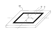
- FIG. 2 shows the coordinate axis representing the position on the mask and the light shielding frame 21 formed on the mask with the center of the 6-inch square reflective mask 200 as the origin.
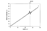
- FIG. 3 shows the result of calculating the positional deviation (positional change amount) in the X direction for each point on the film surface on the X axis, using the simulation for structural analysis described above.
- the light shielding frame 21 is formed between a position of 52 mm and a position of 54 mm in the X-axis direction from the center of the substrate and has a width of 2 mm.
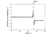
- FIG. 4 is a diagram obtained by subtracting the result of calculating the deviation amount in the X direction in the same manner in the absence of the light shielding frame 21 from the result of FIG. 3, and represents the difference in displacement amount in the X axis direction depending on the presence or absence of the light shielding frame 21.
- the displacement can be calculated from the structural analysis simulation. Further, the positional change amount of each point in the Y-axis direction can be calculated in the same manner as in the X-axis direction.
- the pattern position shift due to the formation of the light shielding frame 21 is corrected by using the change amount of the pattern position obtained from the simulation software for structure analysis and the experiment in this way.
- FIG. 5 is a schematic plan view of the reflective mask 200.
- the reflective mask 200 includes a light shielding frame 21 and a pattern region 22 having a substantially square outer edge when the upper surface is viewed from the front.
- FIG. 6 is an enlarged view of the vicinity of one side of the square of the light shielding frame 21, and shows a position correction area 23 for correcting a positional deviation of the pattern.
- the position correction area 23 is at most 5000 ⁇ m in the vertical direction from the end of the light shielding frame 21.
- the position correction region 23 is a direction orthogonal to one side of the light shielding frame 21 from a straight line that forms the outer edge of the end of the pattern region 22 that is a boundary position with the light shielding frame 21 when the upper surface of the reflective mask 200 is viewed from the front.
- This is a frame-like region having a width of 5000 ⁇ m or less as measured toward the center of the reflective mask 200.
- the upper limit value of 5000 ⁇ m of the width of the position correction region 23 is a viewpoint in which the light shielding frame 21 and the pattern region 22 are efficiently arranged on the mask.
- the upper limit value of the width can be appropriately set according to the shape and dimensions of the reflective mask to be applied, the desired pattern region 22 and the desired light shielding frame 21.
- the shape of the light shielding frame 21 may be other than a square, for example, a rectangular shape.
- the width of the light shielding frame 21 may be formed so that the length is different between the long side and the short side, for example.
- a plurality of chip patterns can be formed in the pattern region 22 to cope with multi-sided layout.
- the portion corresponding to the position correction area 23 of the pattern area 22 is determined according to the position change amount calculated by a prior dynamic simulation or experiment.
- the circuit pattern is drawn using the corrected design data.
- the reflective mask manufacturing method according to the embodiment of the present invention as a method of performing correction processing on design data and generating corrected design data, first, as shown in FIG.
- the data of the pattern area 22 in the area 23 can be divided into a plurality of segments 24.
- FIG. 7 illustrates a state in which the position correction area 23 is divided into a plurality of segments 24 at equal intervals d.
- the positional deviation is corrected in a state where the segment 24 is divided and the multilayer reflective layer 02 is deformed based on the positional deviation amount of the pattern position obtained from the structural analysis simulation or experiment. Even if it exists, it can do by setting the arrangement position of the segment 24 in the design data after correction so that the pattern position is in a state close to the design value or close to the design value.
- the correction amount to be applied to the arrangement of each segment 24 is a correction calculated using a polynomial approximate expression by fitting the relationship between the position change amount calculated by experiment or dynamic simulation and the distance between the light shielding frames 21 using a polynomial approximate expression. Use quantity.
- one point or one side of the pattern data is fixed, and the positional deviation of the pattern position is corrected by correcting the magnification in the correction area. That is, the dimension of the circuit pattern included in the position correction area 23 can be changed.
- FIG. 8A shows a corner (corner) of the light shielding frame 21 and a position correction region 23 in the vicinity of the corner.
- a correction target range is fixed at a point 26 fixed in the position correction area 23, and magnification correction is performed, or FIG.
- FIG. 8C and FIG. 8D there is a method in which the correction target range is fixed at the side 27 to which the correction area is fixed, and magnification correction is performed.
- the correction factor 1 / (1 + a) can be calculated using a which is a coefficient of x in the linear approximation formula, and this value is set as the correction factor.
- the present invention does not limit the approximation expression, and may use a second-order or higher-order polynomial or other function, or may divide the position correction region 23 into a plurality of parts. May be obtained.
- the position correction area 23 is shown having a width of about 0.5 mm from the position of about 51.5 mm to the position of about 52.0 mm from the mask center.
- the width of the position correction region 23 is not limited to 0.5 mm, and can be set with a value obtained by an empirical rule. The present inventors have found that when the width from the end position of the pattern region 22 is 100 ⁇ m or more and 200 ⁇ m or less, the position correction region 23 overlaps the region most distorted by digging, and the correction effect is great.
- Processing for dividing such data into a plurality of segments 24, pattern position arrangement, and data magnification correction can be performed by mask data preparation (MDP) software. Further, in the embodiment of the present invention, it is possible to perform correction by performing magnification correction for each segment 24 by combining division of the segment 24 and magnification correction. Since the distortion of the multilayer reflective layer 02 due to the digging increases as it goes from the center of the mask toward the end of the pattern region 22 as shown in FIG. 4, the correction amount applied to each segment 24 is specifically: It is calculated so as to increase in a staircase (step) direction from the center of the mask toward the end.
- pattern position correction methods include a method for correcting the drawing position when drawing the original design data.
- the drawing driving position correction method corrects the drawing driving position so that the pattern position becomes as designed when the light shielding frame 21 is formed, based on the positional deviation amount of the pattern position obtained from structural analysis simulation or experiment. There is a way to do it. In other words, the circuit pattern on the design data side is not corrected, but the part corresponding to the position correction region 23 at the drawing driving position is corrected on the drawing apparatus side according to the position change amount calculated by a prior mechanical simulation or experiment. And draw. Specifically, for example, a drawing correction map is created so as to correct the drawing driving position in consideration of the position shift amount (position change amount) obtained by calculation. A circuit pattern can be actually drawn on the surface of the mask blank using this correction map.
- the length measurement pattern that is formed in the vicinity of the light shielding frame 21 and is formed to obtain information on the amount of change in position includes a corrected pattern and an uncorrected pattern.
- a method of creating an uncorrected pattern there is a method of drawing before or after drawing a pattern obtained by performing correction processing on an uncorrected pattern.
- the length measurement pattern can be composed of an uncorrected length measurement pattern 34 a and a corrected length measurement pattern 34 b so that their shapes and dimensions are different from each other.
- the uncorrected length measurement pattern 34a and the corrected length measurement pattern 34b have a cross shape (plus) when the top surface of the reflective mask 200a is viewed from the front, and are corrected.
- the length measurement pattern 34b has a shape reduced at a fixed rate with respect to the length measurement pattern 34a without correction.
- the uncorrected length measurement pattern 34a forms a basic pattern with respect to the corrected length measurement pattern 34b.
- the uncorrected length measurement pattern 34a and the corrected length measurement pattern 34b As a method of using the uncorrected length measurement pattern 34a and the corrected length measurement pattern 34b, first, an area where the light shielding frame 21 is to be formed (light shielding frame formation scheduled area) on the surface of the reflective mask blank. Two length measurement patterns 34a and 34b are formed in the vicinity of. Then, the respective dimensions of the two length measurement patterns 34a and 34b are measured, and the difference between the dimensions is calculated from the measurement result. Then, after forming the light shielding frame 21 by digging the light shielding frame formation scheduled region, the respective dimensions of the two length measurement patterns 34a and 34b are measured again, and the dimensions of the two length measurement patterns 34a and 34b are measured. Calculate the difference again. By comparing and analyzing the difference in dimension before digging and the difference in dimension after digging, information on the amount of change in position can be obtained.
- another length measurement pattern 34 c is provided in a region outside the light shielding frame 21, and this length measurement pattern 34 c is combined with the length measurement patterns 34 a and 34 b inside the light shielding frame 21.
- Information on the position change amount may be obtained.
- the position of the length measurement pattern 34c outside the light shielding frame 21 is used as a reference position, and the length measurement pattern 34a inside the light shielding frame 21 before and after the duplication of the multilayer reflective layer 02 is made with respect to this length measurement pattern 34c. It is also possible to measure the position and calculate the amount of displacement displaced by digging.
- the length measurement patterns 34a, 34b, and 34c can be formed in shapes other than a cross shape such as a triangular shape or a rectangular shape as long as they are easily distinguishable from simple line shapes generally used in circuit patterns. .
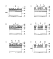
- FIG. 11 and 12A show a reflective mask blank 300 prepared in this embodiment.
- This blank 300 has a 40-layer reflective layer 02 of Mo and Si designed on a substrate 01 so that the reflectance is about 64% with respect to EUV light having a wavelength of 13.5 nm.
- a Ru protective layer 03 having a thickness of 0.5 nm and an absorption layer 04 made of TaSi having a thickness of 70 nm are sequentially formed thereon.
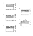
- a positive chemically amplified resist 09 (FEP171: FUJIFILM Electronics Materials) is applied to the blank 300 with a film thickness of 300 nm (FIG. 12B), and first patterned by an electron beam drawing machine (JBX9000: JEOL). After drawing the area and the position correction area, and then drawing the length measurement pattern that has not been corrected in the position correction area, the resist 09 part is obtained by PEB and spray development (SFG3000: Sigma Meltech) at 110 ° C. for 10 minutes. A resist pattern was formed on (FIG. 12C).
- the absorption layer 04 is etched by CF 4 plasma and Cl 2 plasma using a dry etching apparatus (FIG. 12D), and the resist 09 is peeled and washed, thereby measuring the length shown in FIG.
- a reflective mask 301 having a pattern for use was prepared.
- a pattern for length measurement a cross pattern having a width of 2 ⁇ m was arranged on the entire mask at an interval of 1 ⁇ m from the end of the light shielding frame 21.
- a step of forming the light shielding frame 21 was performed on the pattern region 22 of the reflective mask 301 (FIG. 13A) having the above-described length measurement pattern.
- An i-line resist 39 is applied to the reflective mask 301 with a film thickness of 500 nm (FIG. 13B), and is drawn and developed there by an i-line drawing machine (ALTA: Applied Materials), so that a light shielding frame is formed later.
- a resist pattern was formed by removing the region 21 (light shielding frame formation scheduled region 21a) to be 21 (FIG. 13C). At this time, the opening width of the resist pattern was 5 mm, and the resist pattern was arranged at a distance of 3 ⁇ m (micrometer) from the main pattern region 22 of 10 cm ⁇ 10 cm in the center of the mask.
- CHF 3 plasma pressure in the dry etching apparatus 50 mTorr, ICP (inductively coupled plasma) power 500 W, RIE (reactive ion etching) power 2000 W, CHF 3 : flow rate 20 sccm, processing time 6 minutes, These are the same in the following notation), and the absorption layer 04, the protective layer 03, and the multilayer reflective layer 02 at the opening of the resist 39 are penetrated and removed by vertical dry etching (FIG. 13D, ( e)), a shape as shown in FIG. 13 (e) was obtained.
- ICP inductively coupled plasma
- RIE reactive ion etching
- the resist 39 was stripped and washed with a sulfuric stripping solution and ammonia hydrogen peroxide solution to remove the remaining resist 39 by dry etching (FIG. 13 (f)), and a reflective mask 302 was fabricated.
- the length measurement pattern was measured with a pattern position accuracy measuring machine (LMS-IPRO: KLA-Tencor), and the positional deviation of the pattern position due to the formation of the light shielding frame 21 was calculated from the measurement results before and after the light shielding frame 21 was formed.
- LMS-IPRO KLA-Tencor
- the mask data preparation software is used to divide the data of the pattern area 22 in the position correction area 23 near the light shielding frame 21 into a plurality of segments 24, and the data is calculated by the above experiment. Based on the result of the positional deviation of the pattern position due to the formation of 21, data in which the arrangement position of the segment 24 is set so that the pattern position becomes as designed when the light shielding frame 21 is formed was created.
- a mask after the correction processing is again applied by applying the steps described with reference to FIGS. 12 and 13, forming the measurement pattern, forming the light shielding frame 21, and shielding the light.
- the length measurement pattern after the frame 21 was formed was measured.
- FIG. 14B shows the measurement result of the positional deviation amount of the length measurement pattern after the formation of the light shielding frame 21 of the mask after the correction processing.
- the present invention when the present invention is applied, there is no pattern displacement due to the formation of the light shielding frame 21. was confirmed.
- the amount of change in position due to the formation of the light shielding frame 21 was confirmed, and it was also confirmed that the correction amount was appropriate.
- Example 2 For the mask on which the length measurement pattern was drawn in the same manner as in Example 1, the pattern position deviation amount due to the formation of the light shielding frame 21 was calculated from the measurement results before and after the light shielding frame 21 was formed by the pattern position accuracy measuring machine.
- the structural analysis simulation calculation was performed for the amount of misalignment in the vicinity of the light shielding frame 21.
- the Young's modulus and Poisson's ratio of the substrate 01 and the layers 02 to 05 formed on the front and back sides thereof were assumed to be initial values estimated from known literature.
- the above simulation calculation is repeatedly performed by changing the internal stress of the multilayer reflective layer 02, and the physical property value of the material is adjusted as necessary so that the sum of squares of the difference between the measured value of the positional deviation amount and the simulation calculation value is minimized.
- the stress of the multilayer reflection layer 02 was calculated, and it was derived that the internal stress of the multilayer reflection layer 02 was a compressive stress of 420 MPa.
- the average deviation amount in the divided segment 24 was calculated and input to the mask data preparation software as a position correction parameter to create drawing data in which the pattern position in the segment 24 was corrected.
- the positional deviation of the pattern due to the dug of the multilayer reflective layer 02 is a type in which the circuit pattern is formed by dug the multilayer reflective layer 02 up to the substrate 01 inside the pattern region 22 as shown in FIG. This also occurs in the reflective mask 400.
- the main pattern which is a design circuit, is arranged on the entire mask surface, and the engraved patterns influence each other.
- the multilayer reflective layer 02 in FIG. 3 shows a more complicated behavior than the case of the light shielding frame 21 in which only the outer periphery of the main pattern is dug.
- the amount of positional deviation of each position of the main pattern depends on the distance from the edge of the digging portion, that is, the width of the so-called punched portion. In addition, it depends on the width of the remaining portion. This is because when the remaining pattern is formed, since the line width of the remaining portion is thin in the main pattern, the stress is released toward both sides of the remaining pattern.
- the reflective mask 400 of the type in which the multilayer reflective layer 02 is dug the calculation of the dynamic simulation is complicated, but the necessary physical parameters are the same as in the case of the light shielding frame 21 described above. This is possible using a film thickness of 01 to 05, Young's modulus, Poisson's ratio, and internal stress of the multilayer reflective layer 02.
- test pattern assuming a main pattern, for example, a test pattern having the same shape as the main pattern is arranged.
- experiment the required number of times by varying the level of the width of the blank pattern in the test pattern, the width of the blank pattern, the distance between blank patterns, and the distance between blank patterns within the range included in the actual mask. That's fine.
- Reflective mask 400 formed up to formation: reflective mask d: segment length
Landscapes
- Physics & Mathematics (AREA)
- General Physics & Mathematics (AREA)
- Preparing Plates And Mask In Photomechanical Process (AREA)
- Exposure Of Semiconductors, Excluding Electron Or Ion Beam Exposure (AREA)
- Exposure And Positioning Against Photoresist Photosensitive Materials (AREA)
Abstract
反射型マスクの多層反射層を掘り込んでも、掘り込み領域近傍のパターン位置がずれない反射型マスク及びこの反射型マスクの製造方法を提供する。反射型マスクの製造方法は、多層反射層の掘り込みにより、回路パターン、又は前記回路パターンが配置されるパターン領域の外側の少なくとも一部に設けられるEUV光の反射率の低い遮光枠のパターンが形成される反射型マスクに対して、掘り込み領域近傍の回路パターンの位置変化量を、掘り込みに先立つ事前の実験もしくは力学シミュレーションで算出し、算出の結果を元に、掘り込み前に予めずれ量を補正しておき、回路パターンを形成する工程を含む。
Description
本発明は、半導体デバイス等をリソグラフィ技術により製造する際に使用するフォトマスクおよびその製造方法に関する。より詳しくは、極端紫外領域の波長の光を光源としてパターン転写を行う際に適用可能な反射型フォトマスクおよびその製造方法に関する。
半導体集積回路は性能及び生産性を向上させるために微細化、高集積化が進んでおり、回路パターンを形成するためのリソグラフィ技術についても、より微細なパターンを高精度に形成するための技術開発が進められている。これに伴い、パターン形成に使用される露光装置の光源についても短波長化が進められ、波長13.5ナノメートル(nm)の極端紫外光(Extreme Ultraviolet光。以下、「EUV光」と称する。)を用いたパターン転写のプロセスが開発されている。
EUV光を用いるリソグラフィでは従来の193nm等の深紫外光とは異なり、あらゆる物質の屈折率が1に近い値であり、吸収係数も大きいことから、屈折を用いた透過光学系を用いた露光ができない。そこで、屈折率差の大きい材料を交互に積層した多層膜ミラーを用いた反射光学系の露光装置が用いられている。具体的にはモリブデン(Mo)とシリコン(Si)の多層膜が主に用いられる。
マスクについても同様に基板上にモリブデンとシリコンの多層膜を形成した上にEUV光を高効率で吸収する材料で露光パターンを形成する。たとえば吸収パターンの材料としてはタンタル(Ta)を主成分とするものが典型的に用いられ、多層膜の最上層にはルテニウム(Ru)などを成分とする保護膜が形成されているものも使用されている。
反射型マスクを用いて半導体基板上に転写回路パターンを形成する際、一枚の半導体基板上には複数の回路パターンのチップが形成される。隣接するチップ間において、チップ外周部が重なる領域が存在する場合がある。これはウエハ1枚あたりに取れるチップを出来るだけ増加したいという生産性向上のために、チップを高密度に配置するためである。この場合、この領域については複数回(最大で4回)に亘り露光(多重露光)されることになる。この転写パターンのチップ外周部はマスク上でも外周部であり、通常、吸収層の部分である。しかしながら、吸収層上でのEUV光の反射率は、0.5~2%程度あるために、多重露光によりチップ外周部が感光してしまう問題があった。このため、マスク上のチップ外周部に通常の吸収層よりもEUV光の遮光性の高い領域(以下、遮光枠と呼ぶ)を設ける必要性が出てきた。
このような問題を解決するために、反射型マスクの吸収層から多層反射層までを掘り込んだ溝を形成することで多層反射層の反射率を低下させることにより、露光光源波長に対する遮光性の高い遮光枠を設けた反射型マスクが提案されている(例えば、特許文献1参照)。
しかしながら、この遮光枠を形成する為に多層反射層をエッチングにより除去すると、遮光枠の端部で多層膜の応力が開放されることによって位置ずれが生じる。また、このような変形においては、遮光枠の端部に近くになるにしたがって、その位置ずれ量は大きくなる事が想定できる。このことから、遮光枠内にあって遮光枠端部に近いパターンは基板中心から外側に向かって設計値よりもずれてしまうことになる。
このようなずれは、複数の層からなる半導体デバイスを順次リソグラフィ工程にて製造する場合に、各層の重ね合わせ誤差による動作不良の原因となってしまう。また、直接デバイスパターンでなくても、たとえばチップアライメントマークを配置してしまうと、露光装置でアライメント調整しても、設計よりやや縮小されて転写されてしまうことになり、ウエハ上に転写される像の位置精度が低下してしまう要因となってしまう。
またこのような多層反射層を掘り込むことによるパターンの位置ずれは、遮光枠形成時だけでなく、多層反射層を掘り込んで回路パターンを形成する反射型マスクにも同様に発生する。
またこのような多層反射層を掘り込むことによるパターンの位置ずれは、遮光枠形成時だけでなく、多層反射層を掘り込んで回路パターンを形成する反射型マスクにも同様に発生する。
本発明は上記問題点に鑑みてなされたものであり、反射型マスクの多層反射層を掘り込んでも、掘り込み領域近傍のパターン位置がずれない反射型マスクを提供する事を主目的とするものである。
本発明に係る反射型マスクの製造方法のある態様は、
基板、前記基板表面に形成された多層反射層、前記多層反射層の上に形成された保護層及び前記保護層の上に形成された吸収層を備え、前記吸収層、前記保護層及び前記多層反射層の掘り込みにより、回路パターン、又は前記回路パターンが配置されるパターン領域の外側の少なくとも一部に設けられるEUV光の反射率の低い遮光枠のパターンが形成される反射型マスクの製造方法において、前記掘り込みにより形成された掘り込み領域近傍の前記回路パターンの位置変化量を、前記掘り込みに先立つ事前の実験もしくは力学シミュレーションで算出し、前記算出の結果を元に、前記掘り込み前に予めずれ量を補正しておき、前記回路パターンを形成することを特徴とする。
基板、前記基板表面に形成された多層反射層、前記多層反射層の上に形成された保護層及び前記保護層の上に形成された吸収層を備え、前記吸収層、前記保護層及び前記多層反射層の掘り込みにより、回路パターン、又は前記回路パターンが配置されるパターン領域の外側の少なくとも一部に設けられるEUV光の反射率の低い遮光枠のパターンが形成される反射型マスクの製造方法において、前記掘り込みにより形成された掘り込み領域近傍の前記回路パターンの位置変化量を、前記掘り込みに先立つ事前の実験もしくは力学シミュレーションで算出し、前記算出の結果を元に、前記掘り込み前に予めずれ量を補正しておき、前記回路パターンを形成することを特徴とする。
また本発明の請求項2に対応する反射型マスクの製造方法の他の態様は、
請求項1に対応する反射型マスクの製造方法において、前記算出する位置変化量として、前記回路パターンをなす前記掘り込み領域近傍の前記位置変化量を算出することを特徴とする。
請求項1に対応する反射型マスクの製造方法において、前記算出する位置変化量として、前記回路パターンをなす前記掘り込み領域近傍の前記位置変化量を算出することを特徴とする。
また本発明の請求項3に対応する反射型マスクの製造方法の他の態様は、
請求項2に対応する反射型マスクの製造方法において、前記遮光枠の近傍に測長用パターンを形成し、前記測長用パターンを計測することで前記位置変化量の情報を得ることを特徴とする。
請求項2に対応する反射型マスクの製造方法において、前記遮光枠の近傍に測長用パターンを形成し、前記測長用パターンを計測することで前記位置変化量の情報を得ることを特徴とする。
また本発明の請求項4に対応する反射型マスクの製造方法の他の態様は、
請求項3に対応する反射型マスクの製造方法において、前記測長用パターンは前記遮光枠の近傍の補正がされたパターンと補正なしのパターンとから成り、前記補正がされたパターン及び前記補正なしのパターンの差分を計算することで前記位置変化量の情報を得ることができるように、前記測長用パターンを形成することを特徴とする。
請求項3に対応する反射型マスクの製造方法において、前記測長用パターンは前記遮光枠の近傍の補正がされたパターンと補正なしのパターンとから成り、前記補正がされたパターン及び前記補正なしのパターンの差分を計算することで前記位置変化量の情報を得ることができるように、前記測長用パターンを形成することを特徴とする。
また本発明の請求項5に対応する反射型マスクの製造方法の他の態様は、
請求項2に対応する反射型マスクの製造方法において、前記パターン位置の補正手段は、オリジナルの設計データに対して補正処理を行い、補正された設計データを作ることを特徴とする。
請求項2に対応する反射型マスクの製造方法において、前記パターン位置の補正手段は、オリジナルの設計データに対して補正処理を行い、補正された設計データを作ることを特徴とする。
また本発明の請求項6に対応する反射型マスクの製造方法の他の態様は、
請求項4に対応する反射型マスクの製造方法において、前記パターン位置の補正手段は、オリジナルの設計データを描画する際に、描画打ち込み位置を補正することを特徴とする。
請求項4に対応する反射型マスクの製造方法において、前記パターン位置の補正手段は、オリジナルの設計データを描画する際に、描画打ち込み位置を補正することを特徴とする。
また本発明の請求項7に対応する反射型マスクの製造方法の他の態様は、
請求項5又は6に対応する反射型マスクの製造方法において、前記パターン位置の補正を行う領域である位置補正領域は、前記遮光枠の端から大きくとも略5000μm以下であることを特徴とする。
請求項5又は6に対応する反射型マスクの製造方法において、前記パターン位置の補正を行う領域である位置補正領域は、前記遮光枠の端から大きくとも略5000μm以下であることを特徴とする。
また本発明の請求項8に対応する反射型マスクの製造方法の他の態様は、
請求項7に対応する反射型マスクの製造方法において、前記位置補正領域を複数のセグメントに分割し、前記セグメント毎に必要な補正量にて補正することを特徴とする。
請求項7に対応する反射型マスクの製造方法において、前記位置補正領域を複数のセグメントに分割し、前記セグメント毎に必要な補正量にて補正することを特徴とする。
また本発明の請求項9に対応する反射型マスクの製造方法の他の態様は、
請求項8に対応する反射型マスクの製造方法において、前記セグメント毎に適用する補正量は、前記実験もしくは前記力学シミュレーションで算出した前記位置変化量に多項近似式でフィッティングを行い、前記多項近似式を用いて算出された補正量であることを特徴とする。
請求項8に対応する反射型マスクの製造方法において、前記セグメント毎に適用する補正量は、前記実験もしくは前記力学シミュレーションで算出した前記位置変化量に多項近似式でフィッティングを行い、前記多項近似式を用いて算出された補正量であることを特徴とする。
また本発明の請求項10に対応する反射型マスクの製造方法の他の態様は、
請求項9に対応する反射型マスクの製造方法において、前記位置補正領域を複数のセグメントに分割する際は、等間隔に前記位置補正領域を分割することを特徴とする。
請求項9に対応する反射型マスクの製造方法において、前記位置補正領域を複数のセグメントに分割する際は、等間隔に前記位置補正領域を分割することを特徴とする。
また本発明の請求項11に対応する反射型マスクの製造方法の他の態様は、
請求項10に対応する反射型マスクの製造方法において、前記各セグメントの前記遮光枠から垂直方向に測った1辺の長さは、1μmから100μmの範囲であることを特徴とする。
請求項10に対応する反射型マスクの製造方法において、前記各セグメントの前記遮光枠から垂直方向に測った1辺の長さは、1μmから100μmの範囲であることを特徴とする。
また本発明の請求項12に対応する反射型マスクの製造方法の他の態様は、
請求項11に対応する反射型マスクの製造方法において、前記パターン位置の補正方法は、前記位置補正領域の1点あるいは1辺を固定し、前記位置補正領域に対し倍率補正を行うことを特徴とする。
請求項11に対応する反射型マスクの製造方法において、前記パターン位置の補正方法は、前記位置補正領域の1点あるいは1辺を固定し、前記位置補正領域に対し倍率補正を行うことを特徴とする。
また本発明の請求項13に対応する反射型マスクの製造方法の他の態様は、
請求項7に対応する反射型マスクの製造方法において、前記パターン位置の補正方法は、前記位置補正領域を複数のセグメントに分割して補正を行う方法と倍率補正とを組み合わせた方法であることを特徴とする。
請求項7に対応する反射型マスクの製造方法において、前記パターン位置の補正方法は、前記位置補正領域を複数のセグメントに分割して補正を行う方法と倍率補正とを組み合わせた方法であることを特徴とする。
また本発明の請求項14に対応する反射型マスクの製造方法の他の態様は、
請求項6に対応する反射型マスクの製造方法において、前記回路パターンは、前記遮光枠近傍のパターン位置の前記位置変化量を補正するよう作成された補正マップを用いて描画されることを特徴とする。
請求項6に対応する反射型マスクの製造方法において、前記回路パターンは、前記遮光枠近傍のパターン位置の前記位置変化量を補正するよう作成された補正マップを用いて描画されることを特徴とする。
また本発明の請求項15に対応する反射型マスクの製造方法の他の態様は、
請求項2に対応する反射型マスクの製造方法において、前記遮光枠近傍の回路パターンの前記位置変化量を求める前記実験に用いる反射型マスクブランクの多層反射層の持つ応力は、本番に使用する反射型マスクブランクの多層反射層の持つ応力と同程度であることを特徴とする。
請求項2に対応する反射型マスクの製造方法において、前記遮光枠近傍の回路パターンの前記位置変化量を求める前記実験に用いる反射型マスクブランクの多層反射層の持つ応力は、本番に使用する反射型マスクブランクの多層反射層の持つ応力と同程度であることを特徴とする。
また本発明の請求項16に対応する反射型マスクの製造方法の他の態様は、
請求項2に対応する反射型マスクの製造方法において、前記遮光枠近傍の回路パターンの前記位置変化量を求める前記実験は、前記遮光枠を形成する前に測長用パターンを形成及び計測し、前記計測後に前記遮光枠を形成し、再度、前記測長用パターンを計測することで、前記位置変化量を求めることを特徴とする。
請求項2に対応する反射型マスクの製造方法において、前記遮光枠近傍の回路パターンの前記位置変化量を求める前記実験は、前記遮光枠を形成する前に測長用パターンを形成及び計測し、前記計測後に前記遮光枠を形成し、再度、前記測長用パターンを計測することで、前記位置変化量を求めることを特徴とする。
また本発明の請求項17に対応する反射型マスクの製造方法の他の態様は、
請求項1に対応する反射型マスクの製造方法において、前記遮光枠近傍の回路パターンの前記位置変化量を求める前記力学シミュレーションは、前記反射型マスクブランクを構成する各材料のヤング率、ポアソン比及び膜厚と、前記多層反射層の内部応力とを用いて、前記遮光枠形成後のマスク表面の前記位置変化量を見積もることを特徴とする。
請求項1に対応する反射型マスクの製造方法において、前記遮光枠近傍の回路パターンの前記位置変化量を求める前記力学シミュレーションは、前記反射型マスクブランクを構成する各材料のヤング率、ポアソン比及び膜厚と、前記多層反射層の内部応力とを用いて、前記遮光枠形成後のマスク表面の前記位置変化量を見積もることを特徴とする。
また本発明の請求項18に対応する反射型マスクの製造方法の他の態様は、
請求項1に対応する反射型マスクの製造方法において、前記算出する位置変化量として、前記回路パターンをなす前記掘り込み領域近傍の前記位置変化量を算出することを特徴とする。
請求項1に対応する反射型マスクの製造方法において、前記算出する位置変化量として、前記回路パターンをなす前記掘り込み領域近傍の前記位置変化量を算出することを特徴とする。
また本発明の請求項19に対応する反射型マスクの製造方法の他の態様は、
請求項1に対応する反射型マスクの製造方法において、前記遮光枠をなす前記掘り込み領域近傍の前記位置変化量と、前記回路パターンをなす前記掘り込み領域近傍の前記位置変化量とを、両方算出することを特徴とする。
請求項1に対応する反射型マスクの製造方法において、前記遮光枠をなす前記掘り込み領域近傍の前記位置変化量と、前記回路パターンをなす前記掘り込み領域近傍の前記位置変化量とを、両方算出することを特徴とする。
また本発明の請求項20に対応する反射型マスクのある態様は、
請求項1~請求項19のいずれか一項に対応する反射型マスクの製造方法を用いて作製した反射型マスクである。
請求項1~請求項19のいずれか一項に対応する反射型マスクの製造方法を用いて作製した反射型マスクである。
本発明を実施することにより、多層反射層の除去による掘り込み領域を形成する反射型マスクにおいて、掘り込み領域近傍のパターンの位置ずれを制御することが可能となる。
以下に、本発明を実施する形態について図面を用いてさらに詳しく具体的に説明する。以下の図1~図14を用いて説明する反射型マスクの製造方法は、反射型マスクの多層反射層を掘り込んで遮光枠部を形成しても、遮光枠部近傍のパターン位置がずれない反射型マスクを提供するものである。
<反射型EUVマスクの構造>
図1は一般的なEUVマスクブランク100の断面を図示したものである。EUVマスクブランク100は基板01と、基板01の上に設けられEUV光を反射する多層反射層02と、多層反射層02の上に設けられた保護層03と、保護層03の上に設けられパターンが形成される吸収層04とを備える。があり、また、上記各層を形成する基板面の裏側には静電チャックを使用するための導電膜05が形成されている。
図1は一般的なEUVマスクブランク100の断面を図示したものである。EUVマスクブランク100は基板01と、基板01の上に設けられEUV光を反射する多層反射層02と、多層反射層02の上に設けられた保護層03と、保護層03の上に設けられパターンが形成される吸収層04とを備える。があり、また、上記各層を形成する基板面の裏側には静電チャックを使用するための導電膜05が形成されている。
基板01としてはたとえば酸化チタンを含む酸化ケイ素からなる超低熱膨張ガラス(LowThermal Expansion Material、以下LTEMと略記する場合もある)が用いられる。EUV光を反射する多層反射層02としては、光の波長が13.5nmの場合、珪素とモリブデンをおおよそ4nm、3nmの膜厚として交互に40ないし50対積層したものが用いられる。多層反射層02の表面には、多層反射層02の表面を保護するための膜が形成されていることが多く、キャッピング層などと称している。吸収層04はEUV光を吸収する性質の物質であり、たとえばタンタルを主成分とする膜が用いられ、パターン欠陥検査の感度を高める等の目的で多層構造となっている場合もある。
本発明の実施の形態で示したEUV光の反射率の低い遮光枠21の形態は、反射型マスクの吸収層04から多層反射層02までを掘り込んだ溝であり、この遮光枠21を形成することで多層反射層02の反射率を低下させることにより、露光光源波長に対する遮光性の高い遮光枠21を設けた反射型マスクが構成される。
(位置変化量の算出方法)
一般に多層反射層は圧縮方向の内部応力を持っている。多層反射層を枠状にエッチング除去すると、多層反射層が途切れる端面のところで圧縮応力が開放される。LTEMとして用いられているガラスと多層反射層の弾性係数を比較すると、多層反射層の方が数倍大きい。このため、遮光枠内側においては外側に向かって、遮光枠外側では内側に向かって多層反射層が伸びる方向に変形し、これに伴う変形にガラスが反発する力がつりあうところで止まることになる。
一般に多層反射層は圧縮方向の内部応力を持っている。多層反射層を枠状にエッチング除去すると、多層反射層が途切れる端面のところで圧縮応力が開放される。LTEMとして用いられているガラスと多層反射層の弾性係数を比較すると、多層反射層の方が数倍大きい。このため、遮光枠内側においては外側に向かって、遮光枠外側では内側に向かって多層反射層が伸びる方向に変形し、これに伴う変形にガラスが反発する力がつりあうところで止まることになる。
このような変形による、回路パターンのそれぞれの位置の変化量はLTEMや多層反射層02、保護層03及び吸収層04等の反射型マスクブランク100を構成する各材料01~05についてのポアソン比やヤング率などの物性値を用いて、構造解析用のシミュレーションソフトウェアで計算することができる。
また多層反射層02の応力については、多層反射層02を形成する前後の表面の平坦度を計測し、応力によって生じたたわみ量から計測することができる。たとえば、曲率半径と応力の関係を表わすストーニーの式と呼ばれる式を適用しても良いし、より精密には構造解析用のソフトウェアで計算した結果とのフィッティングにより求めてもよい。
図2は6インチ角の反射型マスク200の中心を原点として、マスク上の位置を表す座標軸とマスク上に形成した遮光枠21を示している。上記の構造解析用のシミュレーションを用いて、X軸上の膜表面の各点についてX方向の位置ずれ(位置変化量)を計算した結果を図3に示す。ここで遮光枠21は基板の中心からX軸方向に52mmの位置から54mmの位置の間に形成され2mm幅である。
基板中心から端部に向かって直線的に変位量が大きくなっているのは、多層反射層02及び基板01の圧縮応力によって基板01全体が凸状にたわんでいるためである。遮光枠21が無い状態で同様にX方向のずれ量を計算した結果を図3の結果から差引いたものが図4であり、遮光枠21の有無によるX軸方向の変位量の差を表わしている。 すなわち図4中には、基板01全体のたわみの影響をキャンセルした、各点のより正確な位置変化量が示されている。例えばX=52mmの、遮光枠21に面するパターン領域22の端部をなす位置では、遮光枠21の形成前後で約6nmの位置変化量が生じたことがわかる。
このように構造解析のシミュレーションから位置ずれの計算は可能である。またY軸方向の各点の位置変化量も、X軸方向の場合と同様に計算可能である。こうした掘り込みに先立つ事前の力学シミュレーション以外の他の方法として、実際に図1に示したマスクブランク100を用いて、本番用のマスクブランクと同程度の多層反射層の応力を有するテスト用のマスクブランク100を作成し、このマスクブランク100の表面を掘り込んで遮光枠21を形成し、遮光枠21形成前後のパターン位置を測定する実験により、その遮光枠21の有無による位置ずれの差を求める事ができる。
本発明は、このようにして構造解析用のシミュレーションソフトウェアや実験から求められたパターン位置の変化量を用いて、遮光枠21形成によるパターン位置ずれを補正する。
(パターン位置の補正方法)
図5は反射型マスク200の概略平面図であり、反射型マスク200は、上面を正面から見て略正方形状の外縁を有する遮光枠21とパターン領域22を含む。図6は遮光枠21の正方形の一辺の近傍を拡大した図で、パターンの位置ずれを補正する位置補正領域23が示されている。この位置補正領域23は遮光枠21の端から垂直方向に大きくとも5000μmとする。
すなわち位置補正領域23は、反射型マスク200の上面を正面から見て、遮光枠21との境界位置となるパターン領域22の端部の外縁をなす直線から、遮光枠21の一辺に直交する方向で反射型マスク200の中心側に向かって測って、5000μm以下の幅を有する額縁状の領域である。
図5は反射型マスク200の概略平面図であり、反射型マスク200は、上面を正面から見て略正方形状の外縁を有する遮光枠21とパターン領域22を含む。図6は遮光枠21の正方形の一辺の近傍を拡大した図で、パターンの位置ずれを補正する位置補正領域23が示されている。この位置補正領域23は遮光枠21の端から垂直方向に大きくとも5000μmとする。
すなわち位置補正領域23は、反射型マスク200の上面を正面から見て、遮光枠21との境界位置となるパターン領域22の端部の外縁をなす直線から、遮光枠21の一辺に直交する方向で反射型マスク200の中心側に向かって測って、5000μm以下の幅を有する額縁状の領域である。
本発明の実施の形態に係る6インチ角の反射型マスク200においては、位置補正領域23の幅の上限値である5000μmは、マスク上に遮光枠21及びパターン領域22を効率的に配置する観点から設定されているが、この幅の上限値は適用する反射型マスク、所望のパターン領域22及び所望の遮光枠21のそれぞれの形状及び寸法に応じて適宜設定できる。
尚、遮光枠21の形状は正方形以外の他の形状、例えば矩形状等でも構成できる。また遮光枠21の幅は、例えば長辺と短辺で長さが異なるように形成されてもよい。またパターン領域22の中に複数のチップパターンを形成して多面付けに対応させることもできる。
尚、遮光枠21の形状は正方形以外の他の形状、例えば矩形状等でも構成できる。また遮光枠21の幅は、例えば長辺と短辺で長さが異なるように形成されてもよい。またパターン領域22の中に複数のチップパターンを形成して多面付けに対応させることもできる。
パターン位置の位置ずれを補正する手段としては、例えば回路パターンのオリジナルの設計データにおける、パターン領域22の位置補正領域23に対応する部分を、事前の力学シミュレーションや実験により算出した位置変化量に応じて補正し、補正された設計データを用いて回路パターンを描画する。
本発明の実施の形態に係る反射型マスクの製造方法における、設計データに対して補正処理を行い、補正された設計データを作る方法として、まず図7に示すように遮光枠21近傍の位置補正領域23内におけるパターン領域22のデータを複数のセグメント24に分割することができる。
本発明の実施の形態に係る反射型マスクの製造方法における、設計データに対して補正処理を行い、補正された設計データを作る方法として、まず図7に示すように遮光枠21近傍の位置補正領域23内におけるパターン領域22のデータを複数のセグメント24に分割することができる。
位置補正領域23内のデータを複数のセグメント24に分割する際は等間隔に位置補正領域23内のデータを分割し、そのセグメント24の遮光枠21から垂直方向の1辺の長さdは1μmから100μmの範囲で設定する(1μm≦d≦100μm)。
尚、図7中には、位置補正領域23が、いずれも等間隔dで複数のセグメント24に分割された状態が例示されている。
尚、図7中には、位置補正領域23が、いずれも等間隔dで複数のセグメント24に分割された状態が例示されている。
位置ずれの補正は、構造解析シミュレーションや実験から求められたパターン位置の位置ずれ量をもとに、分割されたセグメント24を、遮光枠21が形成され多層反射層02の変形が生じた状態であっても、パターン位置が設計値通り、或いは設計値に近づく状態になるように、補正後の設計データにおけるセグメント24の配置位置を設定する事によってできる。
各セグメント24の配置に適用する補正量は、実験もしくは力学シミュレーションで算出した位置変化量と遮光枠21の距離の関係に多項近似式でフィッティングを行い、その多項近似式を用いて算出された補正量を用いる。
セグメント24の分割以外の別の補正方法としては、パターンデータの1点あるいは1辺を固定し、補正領域に倍率補正を行うことでパターン位置の位置ずれを補正する。すなわち位置補正領域23の中に含まれる回路パターンの寸法を変化させることができる。
図8(a)は遮光枠21の隅部(コーナー)と、この隅部の近傍にある位置補正領域23を表している。この位置補正領域23に対して倍率補正を行う方法は、図8(b)に示すように位置補正領域23の固定する点26で補正対象範囲を固定し、倍率補正を行う方法、もしくは図8(c)や図8(d)に示すように補正領域の固定する辺27で補正対象範囲を固定し、倍率補正を行う方法がある。
倍率補正を行う際に適用する倍率は、図9に示すように位置補正領域23の遮光枠21形成によるパターン位置の位置ずれ量に対して、一次近似式(Y=aX+b)にてフィッティングを行い、その一次近似式のxの係数であるaを用いて、補正倍率=1/(1+a)から計算する事ができ、この値を補正倍率とする。
ここでは一次近似式にてフィッティングしているが、本発明は近似式を制限するものではなく、二次以上の多項式やその他の関数を用いてもよいし、位置補正領域23を分割して複数の一次近似式を求めてもよい。
また図9中では、位置補正領域23は、マスク中心から約51.5mmの位置から約52.0mmの位置までの間で約0.5mmの幅を有して示されている。しかし位置補正領域23の幅は0.5mmに限定されることなく、経験則により得られた値で設定することもできる。本発明者らは、パターン領域22の端部の位置からの幅が100μm以上200μm以下の場合、位置補正領域23が掘り込みによって最もひずむ領域に重なり、補正の効果が大きいという知見を得た。
また図9中では、位置補正領域23は、マスク中心から約51.5mmの位置から約52.0mmの位置までの間で約0.5mmの幅を有して示されている。しかし位置補正領域23の幅は0.5mmに限定されることなく、経験則により得られた値で設定することもできる。本発明者らは、パターン領域22の端部の位置からの幅が100μm以上200μm以下の場合、位置補正領域23が掘り込みによって最もひずむ領域に重なり、補正の効果が大きいという知見を得た。
このようなデータを複数のセグメント24に分割する処理、パターン位置の配置およびデータの倍率補正は、マスクデータ・プレパレーション(MDP)ソフトウェアによって行うことができる。
また本発明の実施の形態においては、セグメント24の分割と倍率補正とを組み合わせて、セグメント24毎に倍率補正を行って補正することができる。掘り込みによる多層反射層02のひずみは、図4に示したようにマスクの中心からパターン領域22の端部に向かうに従って大きくなるため、各セグメント24に適用する補正量は、具体的には、マスクの中心から端部に向かうに従って、階段(ステップ)状に増加するようにそれぞれ算出される。
また本発明の実施の形態においては、セグメント24の分割と倍率補正とを組み合わせて、セグメント24毎に倍率補正を行って補正することができる。掘り込みによる多層反射層02のひずみは、図4に示したようにマスクの中心からパターン領域22の端部に向かうに従って大きくなるため、各セグメント24に適用する補正量は、具体的には、マスクの中心から端部に向かうに従って、階段(ステップ)状に増加するようにそれぞれ算出される。
その他のパターン位置の補正方法は、オリジナルの設計データを描画する際に、描画打ち込み位置を補正する方法がある。
描画打ち込み位置の補正方法は、構造解析シミュレーションや実験から求められたパターン位置の位置ずれ量をもとに、遮光枠21形成時にパターン位置が設計値通りになるように、描画の打ち込み位置を補正する方法がある。すなわち設計データ側の回路パターンに補正を施すのではなく、描画装置側で描画打ち込み位置における位置補正領域23に対応する部分を、事前の力学シミュレーションや実験により算出した位置変化量に応じて補正して描画を行う。
具体的には例えば、算出して求められた位置ずれ量(位置変化量)を考慮して、描画打ち込み位置を補正するように、描画用の補正マップを作成する。そしてこの補正マップを用いて、マスクブランクの表面に回路パターンを実際に描画することができる。
具体的には例えば、算出して求められた位置ずれ量(位置変化量)を考慮して、描画打ち込み位置を補正するように、描画用の補正マップを作成する。そしてこの補正マップを用いて、マスクブランクの表面に回路パターンを実際に描画することができる。
位置変化量の情報を得る為に形成する、遮光枠21の近傍に配置する測長用パターンは、補正がされたパターンと補正なしのパターンから成る。補正されていないパターンを作成する方法としては、補正されていないパターンを補正処理したパターンの描画前もしくは後に描画する方法がある。
図10中に例示するように、測長用パターンは、それぞれの形状や寸法が互いに異なるように、補正なしの測長用パターン34aと、補正がされた測長用パターン34bとで構成できる。図10中では、補正なしの測長用パターン34a及び補正がされた測長用パターン34bは、いずれも反射型マスク200aの上面を正面から見て十字(プラス)形状であり、補正がされた測長用パターン34bは、補正なしの測長用パターン34aに対して一定の割合で縮小された形状で構成されている。補正なしの測長用パターン34aは補正がされた測長用パターン34bに対する基本パターンをなす。
補正なしの測長用パターン34a及び補正がされた測長用パターン34bの使用方法としては、まず反射型マスクブランクの表面上で、遮光枠21が形成される予定領域(遮光枠形成予定領域)の近傍に、2個の測長用パターン34a,34bを形成する。そして2個の測長用パターン34a,34bのそれぞれの寸法を計測し、計測結果から互いの寸法の差分を算出する。
そして遮光枠形成予定領域を掘り込んで遮光枠21を形成した後、2個の測長用パターン34a,34bのそれぞれの寸法を再度計測し、2個の測長用パターン34a,34bの寸法の差分を再度算出する。掘り込み前の寸法の差分と掘り込み後の寸法の差分を比較して解析することにより、位置変化量の情報を得ることができる。
そして遮光枠形成予定領域を掘り込んで遮光枠21を形成した後、2個の測長用パターン34a,34bのそれぞれの寸法を再度計測し、2個の測長用パターン34a,34bの寸法の差分を再度算出する。掘り込み前の寸法の差分と掘り込み後の寸法の差分を比較して解析することにより、位置変化量の情報を得ることができる。
また図10に示すように、遮光枠21の外側の領域に、別の測長用パターン34cを設け、この測長用パターン34cを、遮光枠21の内側の測長用パターン34a,34bと組み合わせて位置変化量の情報を得てもよい。例えば遮光枠21の外側の測長用パターン34cの位置を基準位置とし、この測長用パターン34cに対する、遮光枠21の内側の測長用パターン34aの、多層反射層02の掘り込みの前後の位置をそれぞれ計測し、掘り込みによってずれた変位量を算出することもできる。
尚、測長用パターン34a,34b,34cは、回路パターンに一般的に用いられる単純なライン形状と見分け易いような形状であれば、三角形状や矩形状等といった十字形状以外の形状でも構成できる。
尚、測長用パターン34a,34b,34cは、回路パターンに一般的に用いられる単純なライン形状と見分け易いような形状であれば、三角形状や矩形状等といった十字形状以外の形状でも構成できる。
以上のようにして、遮光枠21形成による位置ずれが補正された反射型マスク200,200aを得る事ができる。
(実施例1)
以下に本発明の実施例を示す。図11及び図12(a)は本実施例で用意した反射型マスクブランク300を示す。このブランク300は基板01の上に、波長13.5nmのEUV光に対して反射率が64%程度となるように設計されたMoとSiの40ペアの多層反射層02が、その上に2.5nm厚のRuの保護層03が、更にその上に70nm厚のTaSiからなる吸収層04が、順次形成されている。
以下に本発明の実施例を示す。図11及び図12(a)は本実施例で用意した反射型マスクブランク300を示す。このブランク300は基板01の上に、波長13.5nmのEUV光に対して反射率が64%程度となるように設計されたMoとSiの40ペアの多層反射層02が、その上に2.5nm厚のRuの保護層03が、更にその上に70nm厚のTaSiからなる吸収層04が、順次形成されている。
まずは遮光枠21形成によるパターンの位置ずれを算出する為の条件出しマスクを作製した。
本ブランク300に対し、ポジ型化学増幅レジスト09(FEP171:富士フイルムエレクトロニクスマテリアルズ)を300nmの膜厚で塗布し(図12(b))、電子線描画機(JBX9000:日本電子)によってまずパターン領域と位置補正領域を描画し、その後補正処理をしていない測長用パターンを位置補正領域内に描画後、110℃、10分のPEBおよびスプレー現像(SFG3000:シグマメルテック)により、レジスト09部分にレジストパターンを形成した(図12(c))。
次いで、ドライエッチング装置を用いて、CF4プラズマとCl2プラズマにより、吸収層04をエッチングし(図12(d))、レジスト09を剥離洗浄することで、図12(e)に示す測長用パターンを有する反射型マスク301を作製した。測長用パターンは幅2μmの十字パターンを遮光枠21の端から1μmの間隔でマスク全面に配置した。
次いで、測長用パターンをパターン位置精度測定機(LMS-IPRO:ケーエルエー・テンコール)で測定した。
次いで、上述の測長用パターンを有する反射型マスク301(図13(a))のパターン領域22に対して、遮光枠21を形成する工程を行った。反射型マスク301にi線レジスト39を500nmの膜厚で塗布し(図13(b))、そこへi線描画機(ALTA:アプライドマテリアルズ)により描画、現像を行うことにより、後に遮光枠21となる領域(遮光枠形成予定領域21a)を抜いたレジストパターンを形成した(図13(c))。このときレジストパターンの開口幅は5mmとし、マスク中心部の10cm×10cmのメインパターン領域22から3μm(マイクロメートル)の距離に配置した。
次いで、ドライエッチング装置を用いてCHF3プラズマ(ドライエッチング装置内の圧力50mTorr、ICP(誘導結合プラズマ)パワー500W、RIE(反応性イオンエッチング)パワー2000W、CHF3:流量20sccm、処理時間6分、これらは、以下の表記で同じ。)により、上記レジスト39の開口部の吸収層04と保護層03と多層反射層02とを垂直性ドライエッチングで貫通・除去し(図13(d)、(e))、図13(e)に示すような形状を得た。
次いで、硫酸系の剥離液とアンモニア過酸化水素水により、レジスト39剥離・洗浄を実施し、ドライエッチングで残ったレジスト39を除去し(図13(f))、反射型マスク302を作製した。
最後に、測長用パターンをパターン位置精度測定機(LMS-IPRO:ケーエルエー・テンコール)で測定し、遮光枠21形成前後の測定結果から遮光枠21形成によるパターン位置の位置ずれを算出した。
次いで、マスクデータ・プレパレーション・ソフトウェアを用いて、遮光枠21近傍の位置補正領域23内におけるパターン領域22のデータを複数のセグメント24に分割し、そのデータを上記の実験により算出された遮光枠21形成によるパターン位置の位置ずれ結果をもとに、遮光枠21形成時にパターン位置が設計値通りになるように、セグメント24の配置位置を設定したデータを作成した。
次いで、補正処理を行ったデータを用いて、再度補正処理後のマスクを図12、図13で説明した工程を適用して作製を行い、測長用パターンの形成、遮光枠21の形成、遮光枠21形成後の測長用パターンの測定を行った。
最後に条件出しマスク302の遮光枠21形成による測長用パターンの位置ずれ量の測定結果を図14(a)に従来のマスクとして示す。また補正処理後のマスクの遮光枠21形成後の測長用パターンの位置ずれ量の測定結果を図14(b)に示す。従来のマスクでは遮光枠21端部(X=0付近)では6.0nm程度の位置ずれが生じていたが、本発明を適用すると改善されて、遮光枠21形成によるパターンの位置ずれがないことが確認された。また、遮光枠21の近傍に配置した測長用パターンを計測する事で遮光枠21形成による位置変化量を確認し、補正量が適切であることも確認された。
(実施例2)
前記実施例1と同様に測長用パターンを描画したマスクについて、パターン位置精度測定機で遮光枠21形成前後の測定結果から遮光枠21形成によるパターン位置のずれ量を算出した。
前記実施例1と同様に測長用パターンを描画したマスクについて、パターン位置精度測定機で遮光枠21形成前後の測定結果から遮光枠21形成によるパターン位置のずれ量を算出した。
遮光枠21近傍の位置ずれ量について構造解析シミュレーション計算を行った。この計算に必要なパラメータとして、基板01およびその表裏に形成した各層02~05のヤング率およびポアソン比は公知の文献より推定した値を初期値とした。
上記シミュレーション計算を多層反射層02の内部応力を変えて繰り返し計算し、必要に応じて材料の物性値を調整し、位置ずれ量の計測値とシミュレーション計算値の差の二乗和が最小になるような多層反射層02の応力を算出し、多層反射層02の内部応力は420MPaの圧縮応力であることを導出した。
ついで上記分割セグメント24内の平均ずれ量を算出し、マスクデータ・プレパレーション・ソフトウェアに位置補正パラメータとして入力し、セグメント24内のパターン位置を補正した描画データを作成した。
ついで、上記補正した描画データを用いてマスクの作製を行なった。
一方、上記シミュレーション計算を用いることによってパターン位置精度測定機で基板を三点支持する場合の自重によるたわみに起因する見かけの位置ずれ量も計算することができる。この計算結果を用いて、上記補正した描画データを用いて作成したマスクのパターン位置精度を計測したところ、遮光枠21を形成したことによる位置ずれが補正されて設計値との位置ずれ量が小さいマスクが作製できていることを確認した。
<その他の実施の形態>
このような多層反射層02を掘り込むことによるパターンの位置ずれは、図15に示すようなパターン領域22の内側で、多層反射層02を基板01まで掘り込んで回路パターンが形成されたタイプの反射型マスク400にも、同様に発生する。しかしながら、図13(f)に示した反射型マスク302と異なり、設計回路であるメインパターンはマスク全面に配置されており、また掘り込まれたパターン同士が互いに影響し合うため、反射型マスク400における多層反射層02は、メインパターン外周部のみを掘り込んだ遮光枠21の場合と比べて複雑な挙動を示す。
このような多層反射層02を掘り込むことによるパターンの位置ずれは、図15に示すようなパターン領域22の内側で、多層反射層02を基板01まで掘り込んで回路パターンが形成されたタイプの反射型マスク400にも、同様に発生する。しかしながら、図13(f)に示した反射型マスク302と異なり、設計回路であるメインパターンはマスク全面に配置されており、また掘り込まれたパターン同士が互いに影響し合うため、反射型マスク400における多層反射層02は、メインパターン外周部のみを掘り込んだ遮光枠21の場合と比べて複雑な挙動を示す。
具体的には、実施例1に係る遮光枠21の場合と同様に、メインパターンのそれぞれの位置の位置ずれ量は掘り込み部分のエッジからの距離、いわゆる抜き部の幅に依存するが、これに加えて、残し部の幅にも依存する。なぜなら、残しパターンを形成した場合、メインパターンでは残し部の線幅が細いため、残しパターンの両側に向かって応力が開放されるためである。
このように、多層反射層02を掘り込んだタイプの反射型マスク400の場合、力学シミュレーションの計算は複雑にはなるが、必要な物理パラメータは、上述した遮光枠21の場合と同様に、各層01~05の膜厚、ヤング率、ポアソン比、および多層反射層02の内部応力を用いて可能である。
このように、多層反射層02を掘り込んだタイプの反射型マスク400の場合、力学シミュレーションの計算は複雑にはなるが、必要な物理パラメータは、上述した遮光枠21の場合と同様に、各層01~05の膜厚、ヤング率、ポアソン比、および多層反射層02の内部応力を用いて可能である。
事前に実験する方法としては、メインパターンを想定したテストパターン、例えばメインパターンと同じ形状のテストパターン等を配置して行う。この場合、テストパターン等における抜きパターンの線幅、残しパターンの線幅、抜きパターン間の距離、残しパターン間の距離を、実際のマスクに含まれる範囲で水準を振って、必要な回数実験すればよい。
本発明を実施することにより、多層反射層の掘り込みによって遮光枠部や回路パターンを形成する反射型マスクおいて、掘り込み領域近傍のパターンの位置ずれを制御することが可能となる。
01・・・基板
02・・・多層反射層
03・・・保護層
04・・・吸収層
05・・・裏面導電膜
09・・・レジスト
21・・・遮光枠
21a・・・遮光枠形成予定領域
22・・・パターン領域
23・・・位置補正領域
24・・・分割されたパターンデータのセグメント
25・・・倍率補正された補正領域
26・・・データに倍率補正する際に固定する点
27・・・データに倍率補正する際に固定する辺
39・・・レジスト
100・・・EUVマスクブランク(反射型マスクブランク)
200・・・反射型マスク
200a・・・反射型マスク
300・・・本発明で使用するEUVマスクブランク
301・・・本発明でパターン形成まで行った反射型マスク
302・・・本発明で遮光枠形成まで行った反射型マスク
400・・・反射型マスク
d・・・セグメントの長さ
02・・・多層反射層
03・・・保護層
04・・・吸収層
05・・・裏面導電膜
09・・・レジスト
21・・・遮光枠
21a・・・遮光枠形成予定領域
22・・・パターン領域
23・・・位置補正領域
24・・・分割されたパターンデータのセグメント
25・・・倍率補正された補正領域
26・・・データに倍率補正する際に固定する点
27・・・データに倍率補正する際に固定する辺
39・・・レジスト
100・・・EUVマスクブランク(反射型マスクブランク)
200・・・反射型マスク
200a・・・反射型マスク
300・・・本発明で使用するEUVマスクブランク
301・・・本発明でパターン形成まで行った反射型マスク
302・・・本発明で遮光枠形成まで行った反射型マスク
400・・・反射型マスク
d・・・セグメントの長さ
Claims (20)
- 基板、前記基板表面に形成された多層反射層、前記多層反射層の上に形成された保護層及び前記保護層の上に形成された吸収層を備え、前記吸収層、前記保護層及び前記多層反射層の掘り込みにより、回路パターン、又は前記回路パターンが配置されるパターン領域の外側の少なくとも一部に設けられるEUV光の反射率の低い遮光枠のパターンが形成される反射型マスクの製造方法において、
前記掘り込みにより形成された掘り込み領域近傍の前記回路パターンの位置変化量を、前記掘り込みに先立つ事前の実験もしくは力学シミュレーションで算出し、前記算出の結果を元に、前記掘り込み前に予めずれ量を補正しておき、前記回路パターンを形成することを特徴とする反射型マスクの製造方法。 - 請求項1に記載の反射型マスクの製造方法において、前記算出する位置変化量として、前記回路パターンをなす前記掘り込み領域近傍の前記位置変化量を算出することを特徴とする反射型マスクの製造方法。
- 請求項2に記載の反射型マスクの製造方法において、前記遮光枠の近傍に測長用パターンを形成し、前記測長用パターンを計測することで前記位置変化量の情報を得ることを特徴とする反射型マスクの製造方法。
- 請求項3に記載の反射型マスクの製造方法において、前記測長用パターンは前記遮光枠の近傍の補正がされたパターンと補正なしのパターンとから成り、前記補正がされたパターン及び前記補正なしのパターンの差分を計算することで前記位置変化量の情報を得ることができるように、前記測長用パターンを形成することを特徴とする反射型マスクの製造方法。
- 請求項2に記載の反射型マスクの製造方法において、前記パターン位置の補正手段は、オリジナルの設計データに対して補正処理を行い、補正された設計データを作ることを特徴とする反射型マスクの製造方法。
- 請求項4に記載の反射型マスクの製造方法において、前記パターン位置の補正手段は、オリジナルの設計データを描画する際に、描画打ち込み位置を補正することを特徴とする反射型マスクの製造方法。
- 請求項5又は6に記載の反射型マスクの製造方法において、前記パターン位置の補正を行う領域である位置補正領域は、前記遮光枠の端から大きくとも略5000μm以下であることを特徴とする反射型マスクの製造方法。
- 請求項7に記載の反射型マスクの製造方法において、前記位置補正領域を複数のセグメントに分割し、前記セグメント毎に必要な補正量にて補正することを特徴とする反射型マスクの製造方法。
- 請求項8に記載の反射型マスクの製造方法において、前記セグメント毎に適用する補正量は、前記実験もしくは前記力学シミュレーションで算出した前記位置変化量に多項近似式でフィッティングを行い、前記多項近似式を用いて算出された補正量であることを特徴とする反射型マスクの製造方法。
- 請求項9に記載の反射型マスクの製造方法において、前記位置補正領域を複数のセグメントに分割する際は、等間隔に前記位置補正領域を分割することを特徴とする反射型マスクの製造方法。
- 請求項10に記載の反射型マスクの製造方法において、前記各セグメントの前記遮光枠から垂直方向に測った1辺の長さは、1μmから100μmの範囲であることを特徴とする反射型マスクの製造方法。
- 請求項11に記載の反射型マスクの製造方法において、前記パターン位置の補正方法は、前記位置補正領域の1点あるいは1辺を固定し、前記位置補正領域に対し倍率補正を行うことを特徴とする反射型マスクの製造方法。
- 請求項7に記載の反射型マスクの製造方法において、前記パターン位置の補正方法は、前記位置補正領域を複数のセグメントに分割して補正を行う方法と倍率補正とを組み合わせた方法であることを特徴とする反射型マスクの製造方法。
- 請求項6に記載の反射型マスクの製造方法において、前記回路パターンは、前記遮光枠近傍のパターン位置の前記位置変化量を補正するよう作成された補正マップを用いて描画されることを特徴とする反射型マスクの製造方法。
- 請求項2に記載の反射型マスクの製造方法において、前記遮光枠近傍の回路パターンの前記位置変化量を求める前記実験に用いる反射型マスクブランクの多層反射層の持つ応力は、本番に使用する反射型マスクブランクの多層反射層の持つ応力と同程度であることを特徴とする反射型マスクの製造方法。
- 請求項2に記載の反射型マスクの製造方法において、前記遮光枠近傍の回路パターンの前記位置変化量を求める前記実験は、前記遮光枠を形成する前に測長用パターンを形成及び計測し、前記計測後に前記遮光枠を形成し、再度、前記測長用パターンを計測することで、前記位置変化量を求めることを特徴とする反射型マスクの製造方法。
- 請求項1に記載の反射型マスクの製造方法において、前記遮光枠近傍の回路パターンの前記位置変化量を求める前記力学シミュレーションは、前記反射型マスクブランクを構成する各材料のヤング率、ポアソン比及び膜厚と、前記多層反射層の内部応力とを用いて、前記遮光枠形成後のマスク表面の前記位置変化量を見積もることを特徴とする反射型マスクの製造方法。
- 請求項1に記載の反射型マスクの製造方法において、前記算出する位置変化量として、前記回路パターンをなす前記掘り込み領域近傍の前記位置変化量を算出することを特徴とする反射型マスクの製造方法。
- 請求項1に記載の反射型マスクの製造方法において、前記遮光枠をなす前記掘り込み領域近傍の前記位置変化量と、前記回路パターンをなす前記掘り込み領域近傍の前記位置変化量とを、両方算出することを特徴とする反射型マスクの製造方法。
- 請求項1~請求項19のいずれか一項に記載の反射型マスクの製造方法を用いて作製した反射型マスク。
Applications Claiming Priority (2)
| Application Number | Priority Date | Filing Date | Title |
|---|---|---|---|
| JP2014262294A JP2018029091A (ja) | 2014-12-25 | 2014-12-25 | 反射型マスク及びその製造方法 |
| JP2014-262294 | 2014-12-25 |
Publications (1)
| Publication Number | Publication Date |
|---|---|
| WO2016103734A1 true WO2016103734A1 (ja) | 2016-06-30 |
Family
ID=56149791
Family Applications (1)
| Application Number | Title | Priority Date | Filing Date |
|---|---|---|---|
| PCT/JP2015/006487 Ceased WO2016103734A1 (ja) | 2014-12-25 | 2015-12-25 | 反射型マスク及びその製造方法 |
Country Status (3)
| Country | Link |
|---|---|
| JP (1) | JP2018029091A (ja) |
| TW (1) | TW201635006A (ja) |
| WO (1) | WO2016103734A1 (ja) |
Citations (4)
| Publication number | Priority date | Publication date | Assignee | Title |
|---|---|---|---|---|
| JP2010008921A (ja) * | 2008-06-30 | 2010-01-14 | Toshiba Corp | マスクパターンデータの生成方法およびマスクの製造方法 |
| JP2014075484A (ja) * | 2012-10-04 | 2014-04-24 | Toppan Printing Co Ltd | 反射型フォトマスク |
| JP2014183075A (ja) * | 2013-03-18 | 2014-09-29 | Toppan Printing Co Ltd | 反射型マスクおよびその製造方法 |
| JP2014232844A (ja) * | 2013-05-30 | 2014-12-11 | 凸版印刷株式会社 | 反射型マスクの製造方法 |
-
2014
- 2014-12-25 JP JP2014262294A patent/JP2018029091A/ja active Pending
-
2015
- 2015-12-24 TW TW104143495A patent/TW201635006A/zh unknown
- 2015-12-25 WO PCT/JP2015/006487 patent/WO2016103734A1/ja not_active Ceased
Patent Citations (4)
| Publication number | Priority date | Publication date | Assignee | Title |
|---|---|---|---|---|
| JP2010008921A (ja) * | 2008-06-30 | 2010-01-14 | Toshiba Corp | マスクパターンデータの生成方法およびマスクの製造方法 |
| JP2014075484A (ja) * | 2012-10-04 | 2014-04-24 | Toppan Printing Co Ltd | 反射型フォトマスク |
| JP2014183075A (ja) * | 2013-03-18 | 2014-09-29 | Toppan Printing Co Ltd | 反射型マスクおよびその製造方法 |
| JP2014232844A (ja) * | 2013-05-30 | 2014-12-11 | 凸版印刷株式会社 | 反射型マスクの製造方法 |
Also Published As
| Publication number | Publication date |
|---|---|
| JP2018029091A (ja) | 2018-02-22 |
| TW201635006A (zh) | 2016-10-01 |
Similar Documents
| Publication | Publication Date | Title |
|---|---|---|
| US9285672B2 (en) | Reflective mask and method for manufacturing same | |
| JP5970021B2 (ja) | フォトマスクの製造方法、描画装置、フォトマスクの検査方法、フォトマスクの検査装置、及び表示装置の製造方法 | |
| TWI795566B (zh) | 用於執行光學近接校正的方法及使用光學近接校正製造遮罩的方法 | |
| US9235114B2 (en) | Reflective mask and method for manufacturing the same | |
| JP5082902B2 (ja) | フォトマスクの製造方法、フォトマスク製造装置及びフォトマスク | |
| WO2015141230A1 (ja) | 反射型フォトマスクブランク、反射型フォトマスク、反射型フォトマスクの製造方法、露光方法及び露光装置 | |
| JP2004302263A (ja) | マスクパターン補正方法およびフォトマスク | |
| US7930654B2 (en) | System and method of correcting errors in SEM-measurements | |
| WO2015146140A1 (ja) | Euvマスクの位相欠陥評価方法、euvマスクの製造方法、euvマスクブランク及びeuvマスク | |
| JP5356114B2 (ja) | 露光用マスク及び半導体装置の製造方法 | |
| JP6559433B2 (ja) | フォトマスクの製造方法、描画装置、フォトマスクの検査方法、フォトマスクの検査装置、及び表示装置の製造方法 | |
| JP6316036B2 (ja) | フォトマスクの製造方法 | |
| JP5742300B2 (ja) | 反射型マスクブランク及びその製造方法、反射型マスク | |
| JP6418603B2 (ja) | 反射型露光マスクの製造方法およびマスクパターン作製プログラム | |
| JP2017084837A (ja) | 反射型フォトマスクブランクおよび反射型フォトマスクの製造方法ならびに反射型フォトマスク | |
| JP2014191176A (ja) | フォトマスクブランクス、フォトマスク及びその製造方法 | |
| JP2013055197A (ja) | 露光方法及び露光用マスク | |
| JP6135105B2 (ja) | 反射型マスクの製造方法 | |
| WO2016103734A1 (ja) | 反射型マスク及びその製造方法 | |
| JP5347360B2 (ja) | 両面にパターンを有するフォトマスクの作製方法 | |
| JP2014232844A (ja) | 反射型マスクの製造方法 | |
| US9946150B2 (en) | Light reflection type lithography mask, its manufacturing method, mask data generation method and mask blank | |
| JP2015050242A (ja) | 反射型マスク、反射型マスクブランクおよびその製造方法 | |
| JP2014183075A (ja) | 反射型マスクおよびその製造方法 | |
| JP6862703B2 (ja) | 反射型マスク及び反射型マスクの製造方法 |
Legal Events
| Date | Code | Title | Description |
|---|---|---|---|
| 121 | Ep: the epo has been informed by wipo that ep was designated in this application |
Ref document number: 15872305 Country of ref document: EP Kind code of ref document: A1 |
|
| NENP | Non-entry into the national phase |
Ref country code: DE |
|
| NENP | Non-entry into the national phase |
Ref country code: JP |
|
| 122 | Ep: pct application non-entry in european phase |
Ref document number: 15872305 Country of ref document: EP Kind code of ref document: A1 |