WO2016103475A1 - 表示装置及び表示装置の製造方法 - Google Patents
表示装置及び表示装置の製造方法 Download PDFInfo
- Publication number
- WO2016103475A1 WO2016103475A1 PCT/JP2014/084596 JP2014084596W WO2016103475A1 WO 2016103475 A1 WO2016103475 A1 WO 2016103475A1 JP 2014084596 W JP2014084596 W JP 2014084596W WO 2016103475 A1 WO2016103475 A1 WO 2016103475A1
- Authority
- WO
- WIPO (PCT)
- Prior art keywords
- display panel
- signal line
- display
- wiring
- connection
- Prior art date
- Legal status (The legal status is an assumption and is not a legal conclusion. Google has not performed a legal analysis and makes no representation as to the accuracy of the status listed.)
- Ceased
Links
Images




Classifications
-
- G—PHYSICS
- G02—OPTICS
- G02F—OPTICAL DEVICES OR ARRANGEMENTS FOR THE CONTROL OF LIGHT BY MODIFICATION OF THE OPTICAL PROPERTIES OF THE MEDIA OF THE ELEMENTS INVOLVED THEREIN; NON-LINEAR OPTICS; FREQUENCY-CHANGING OF LIGHT; OPTICAL LOGIC ELEMENTS; OPTICAL ANALOGUE/DIGITAL CONVERTERS
- G02F1/00—Devices or arrangements for the control of the intensity, colour, phase, polarisation or direction of light arriving from an independent light source, e.g. switching, gating or modulating; Non-linear optics
- G02F1/01—Devices or arrangements for the control of the intensity, colour, phase, polarisation or direction of light arriving from an independent light source, e.g. switching, gating or modulating; Non-linear optics for the control of the intensity, phase, polarisation or colour
- G02F1/13—Devices or arrangements for the control of the intensity, colour, phase, polarisation or direction of light arriving from an independent light source, e.g. switching, gating or modulating; Non-linear optics for the control of the intensity, phase, polarisation or colour based on liquid crystals, e.g. single liquid crystal display cells
- G02F1/133—Constructional arrangements; Operation of liquid crystal cells; Circuit arrangements
- G02F1/136—Liquid crystal cells structurally associated with a semi-conducting layer or substrate, e.g. cells forming part of an integrated circuit
- G02F1/1362—Active matrix addressed cells
- G02F1/136259—Repairing; Defects
-
- G—PHYSICS
- G02—OPTICS
- G02F—OPTICAL DEVICES OR ARRANGEMENTS FOR THE CONTROL OF LIGHT BY MODIFICATION OF THE OPTICAL PROPERTIES OF THE MEDIA OF THE ELEMENTS INVOLVED THEREIN; NON-LINEAR OPTICS; FREQUENCY-CHANGING OF LIGHT; OPTICAL LOGIC ELEMENTS; OPTICAL ANALOGUE/DIGITAL CONVERTERS
- G02F1/00—Devices or arrangements for the control of the intensity, colour, phase, polarisation or direction of light arriving from an independent light source, e.g. switching, gating or modulating; Non-linear optics
- G02F1/01—Devices or arrangements for the control of the intensity, colour, phase, polarisation or direction of light arriving from an independent light source, e.g. switching, gating or modulating; Non-linear optics for the control of the intensity, phase, polarisation or colour
- G02F1/13—Devices or arrangements for the control of the intensity, colour, phase, polarisation or direction of light arriving from an independent light source, e.g. switching, gating or modulating; Non-linear optics for the control of the intensity, phase, polarisation or colour based on liquid crystals, e.g. single liquid crystal display cells
- G02F1/1306—Details
- G02F1/1309—Repairing; Testing
-
- G—PHYSICS
- G02—OPTICS
- G02F—OPTICAL DEVICES OR ARRANGEMENTS FOR THE CONTROL OF LIGHT BY MODIFICATION OF THE OPTICAL PROPERTIES OF THE MEDIA OF THE ELEMENTS INVOLVED THEREIN; NON-LINEAR OPTICS; FREQUENCY-CHANGING OF LIGHT; OPTICAL LOGIC ELEMENTS; OPTICAL ANALOGUE/DIGITAL CONVERTERS
- G02F1/00—Devices or arrangements for the control of the intensity, colour, phase, polarisation or direction of light arriving from an independent light source, e.g. switching, gating or modulating; Non-linear optics
- G02F1/01—Devices or arrangements for the control of the intensity, colour, phase, polarisation or direction of light arriving from an independent light source, e.g. switching, gating or modulating; Non-linear optics for the control of the intensity, phase, polarisation or colour
- G02F1/13—Devices or arrangements for the control of the intensity, colour, phase, polarisation or direction of light arriving from an independent light source, e.g. switching, gating or modulating; Non-linear optics for the control of the intensity, phase, polarisation or colour based on liquid crystals, e.g. single liquid crystal display cells
- G02F1/133—Constructional arrangements; Operation of liquid crystal cells; Circuit arrangements
- G02F1/136—Liquid crystal cells structurally associated with a semi-conducting layer or substrate, e.g. cells forming part of an integrated circuit
-
- G—PHYSICS
- G09—EDUCATION; CRYPTOGRAPHY; DISPLAY; ADVERTISING; SEALS
- G09G—ARRANGEMENTS OR CIRCUITS FOR CONTROL OF INDICATING DEVICES USING STATIC MEANS TO PRESENT VARIABLE INFORMATION
- G09G3/00—Control arrangements or circuits, of interest only in connection with visual indicators other than cathode-ray tubes
- G09G3/20—Control arrangements or circuits, of interest only in connection with visual indicators other than cathode-ray tubes for presentation of an assembly of a number of characters, e.g. a page, by composing the assembly by combination of individual elements arranged in a matrix no fixed position being assigned to or needed to be assigned to the individual characters or partial characters
- G09G3/34—Control arrangements or circuits, of interest only in connection with visual indicators other than cathode-ray tubes for presentation of an assembly of a number of characters, e.g. a page, by composing the assembly by combination of individual elements arranged in a matrix no fixed position being assigned to or needed to be assigned to the individual characters or partial characters by control of light from an independent source
- G09G3/36—Control arrangements or circuits, of interest only in connection with visual indicators other than cathode-ray tubes for presentation of an assembly of a number of characters, e.g. a page, by composing the assembly by combination of individual elements arranged in a matrix no fixed position being assigned to or needed to be assigned to the individual characters or partial characters by control of light from an independent source using liquid crystals
-
- G—PHYSICS
- G09—EDUCATION; CRYPTOGRAPHY; DISPLAY; ADVERTISING; SEALS
- G09G—ARRANGEMENTS OR CIRCUITS FOR CONTROL OF INDICATING DEVICES USING STATIC MEANS TO PRESENT VARIABLE INFORMATION
- G09G3/00—Control arrangements or circuits, of interest only in connection with visual indicators other than cathode-ray tubes
- G09G3/20—Control arrangements or circuits, of interest only in connection with visual indicators other than cathode-ray tubes for presentation of an assembly of a number of characters, e.g. a page, by composing the assembly by combination of individual elements arranged in a matrix no fixed position being assigned to or needed to be assigned to the individual characters or partial characters
- G09G3/34—Control arrangements or circuits, of interest only in connection with visual indicators other than cathode-ray tubes for presentation of an assembly of a number of characters, e.g. a page, by composing the assembly by combination of individual elements arranged in a matrix no fixed position being assigned to or needed to be assigned to the individual characters or partial characters by control of light from an independent source
- G09G3/36—Control arrangements or circuits, of interest only in connection with visual indicators other than cathode-ray tubes for presentation of an assembly of a number of characters, e.g. a page, by composing the assembly by combination of individual elements arranged in a matrix no fixed position being assigned to or needed to be assigned to the individual characters or partial characters by control of light from an independent source using liquid crystals
- G09G3/3611—Control of matrices with row and column drivers
-
- G—PHYSICS
- G02—OPTICS
- G02F—OPTICAL DEVICES OR ARRANGEMENTS FOR THE CONTROL OF LIGHT BY MODIFICATION OF THE OPTICAL PROPERTIES OF THE MEDIA OF THE ELEMENTS INVOLVED THEREIN; NON-LINEAR OPTICS; FREQUENCY-CHANGING OF LIGHT; OPTICAL LOGIC ELEMENTS; OPTICAL ANALOGUE/DIGITAL CONVERTERS
- G02F1/00—Devices or arrangements for the control of the intensity, colour, phase, polarisation or direction of light arriving from an independent light source, e.g. switching, gating or modulating; Non-linear optics
- G02F1/01—Devices or arrangements for the control of the intensity, colour, phase, polarisation or direction of light arriving from an independent light source, e.g. switching, gating or modulating; Non-linear optics for the control of the intensity, phase, polarisation or colour
- G02F1/13—Devices or arrangements for the control of the intensity, colour, phase, polarisation or direction of light arriving from an independent light source, e.g. switching, gating or modulating; Non-linear optics for the control of the intensity, phase, polarisation or colour based on liquid crystals, e.g. single liquid crystal display cells
- G02F1/133—Constructional arrangements; Operation of liquid crystal cells; Circuit arrangements
- G02F1/136—Liquid crystal cells structurally associated with a semi-conducting layer or substrate, e.g. cells forming part of an integrated circuit
- G02F1/1362—Active matrix addressed cells
- G02F1/136254—Checking; Testing
-
- G—PHYSICS
- G02—OPTICS
- G02F—OPTICAL DEVICES OR ARRANGEMENTS FOR THE CONTROL OF LIGHT BY MODIFICATION OF THE OPTICAL PROPERTIES OF THE MEDIA OF THE ELEMENTS INVOLVED THEREIN; NON-LINEAR OPTICS; FREQUENCY-CHANGING OF LIGHT; OPTICAL LOGIC ELEMENTS; OPTICAL ANALOGUE/DIGITAL CONVERTERS
- G02F1/00—Devices or arrangements for the control of the intensity, colour, phase, polarisation or direction of light arriving from an independent light source, e.g. switching, gating or modulating; Non-linear optics
- G02F1/01—Devices or arrangements for the control of the intensity, colour, phase, polarisation or direction of light arriving from an independent light source, e.g. switching, gating or modulating; Non-linear optics for the control of the intensity, phase, polarisation or colour
- G02F1/13—Devices or arrangements for the control of the intensity, colour, phase, polarisation or direction of light arriving from an independent light source, e.g. switching, gating or modulating; Non-linear optics for the control of the intensity, phase, polarisation or colour based on liquid crystals, e.g. single liquid crystal display cells
- G02F1/133—Constructional arrangements; Operation of liquid crystal cells; Circuit arrangements
- G02F1/136—Liquid crystal cells structurally associated with a semi-conducting layer or substrate, e.g. cells forming part of an integrated circuit
- G02F1/1362—Active matrix addressed cells
- G02F1/136259—Repairing; Defects
- G02F1/136263—Line defects
-
- G—PHYSICS
- G02—OPTICS
- G02F—OPTICAL DEVICES OR ARRANGEMENTS FOR THE CONTROL OF LIGHT BY MODIFICATION OF THE OPTICAL PROPERTIES OF THE MEDIA OF THE ELEMENTS INVOLVED THEREIN; NON-LINEAR OPTICS; FREQUENCY-CHANGING OF LIGHT; OPTICAL LOGIC ELEMENTS; OPTICAL ANALOGUE/DIGITAL CONVERTERS
- G02F1/00—Devices or arrangements for the control of the intensity, colour, phase, polarisation or direction of light arriving from an independent light source, e.g. switching, gating or modulating; Non-linear optics
- G02F1/01—Devices or arrangements for the control of the intensity, colour, phase, polarisation or direction of light arriving from an independent light source, e.g. switching, gating or modulating; Non-linear optics for the control of the intensity, phase, polarisation or colour
- G02F1/13—Devices or arrangements for the control of the intensity, colour, phase, polarisation or direction of light arriving from an independent light source, e.g. switching, gating or modulating; Non-linear optics for the control of the intensity, phase, polarisation or colour based on liquid crystals, e.g. single liquid crystal display cells
- G02F1/133—Constructional arrangements; Operation of liquid crystal cells; Circuit arrangements
- G02F1/136—Liquid crystal cells structurally associated with a semi-conducting layer or substrate, e.g. cells forming part of an integrated circuit
- G02F1/1362—Active matrix addressed cells
- G02F1/136259—Repairing; Defects
- G02F1/136272—Auxiliary lines
-
- G—PHYSICS
- G09—EDUCATION; CRYPTOGRAPHY; DISPLAY; ADVERTISING; SEALS
- G09F—DISPLAYING; ADVERTISING; SIGNS; LABELS OR NAME-PLATES; SEALS
- G09F9/00—Indicating arrangements for variable information in which the information is built-up on a support by selection or combination of individual elements
- G09F9/30—Indicating arrangements for variable information in which the information is built-up on a support by selection or combination of individual elements in which the desired character or characters are formed by combining individual elements
- G09F9/302—Indicating arrangements for variable information in which the information is built-up on a support by selection or combination of individual elements in which the desired character or characters are formed by combining individual elements characterised by the form or geometrical disposition of the individual elements
-
- G—PHYSICS
- G09—EDUCATION; CRYPTOGRAPHY; DISPLAY; ADVERTISING; SEALS
- G09G—ARRANGEMENTS OR CIRCUITS FOR CONTROL OF INDICATING DEVICES USING STATIC MEANS TO PRESENT VARIABLE INFORMATION
- G09G2300/00—Aspects of the constitution of display devices
- G09G2300/04—Structural and physical details of display devices
- G09G2300/0404—Matrix technologies
- G09G2300/0413—Details of dummy pixels or dummy lines in flat panels
-
- G—PHYSICS
- G09—EDUCATION; CRYPTOGRAPHY; DISPLAY; ADVERTISING; SEALS
- G09G—ARRANGEMENTS OR CIRCUITS FOR CONTROL OF INDICATING DEVICES USING STATIC MEANS TO PRESENT VARIABLE INFORMATION
- G09G2300/00—Aspects of the constitution of display devices
- G09G2300/04—Structural and physical details of display devices
- G09G2300/0421—Structural details of the set of electrodes
- G09G2300/0426—Layout of electrodes and connections
-
- G—PHYSICS
- G09—EDUCATION; CRYPTOGRAPHY; DISPLAY; ADVERTISING; SEALS
- G09G—ARRANGEMENTS OR CIRCUITS FOR CONTROL OF INDICATING DEVICES USING STATIC MEANS TO PRESENT VARIABLE INFORMATION
- G09G2330/00—Aspects of power supply; Aspects of display protection and defect management
- G09G2330/08—Fault-tolerant or redundant circuits, or circuits in which repair of defects is prepared
Definitions
- the present invention relates to a display device for displaying video and a method for manufacturing the display device.
- Thin display devices such as liquid crystal display devices, are generally widespread because they have a larger display area than the installation area.
- Thin display devices such as liquid crystal display devices, are generally widespread because they have a larger display area than the installation area.
- a plurality of data signal lines and scanning signal lines are arranged in a matrix.
- a thin film transistor and a pixel electrode connected to the thin film transistor are provided near the intersection of the two.
- the thin film transistor is ON / OFF controlled by the scanning signal line, a signal potential is applied from the data signal line to each pixel electrode, the alignment state of the liquid crystal changes, and information is displayed.
- black lines normally black mode
- bright lines normally white mode
- a spare from the vicinity of the signal input side end of the data signal line to the vicinity of the opposite end of the data signal line (below the display area) through the panel external substrate or the like.
- a signal is input to the portion after the disconnection portion by melt-connecting the end portion (termination portion) of the portion after the disconnection portion of the disconnected data signal line and the spare wiring using a laser or the like.
- the present invention has been made in view of such circumstances, and an object of the present invention is to provide a display device and a method for manufacturing the display device that can reduce the resistance value in the data signal line and the spare wiring.
- a display device includes a display panel having a display area and a non-display area positioned around the display area, a signal line provided in the display panel, for transmitting a video signal, and the display panel It is routed to the outside and the non-display area of the display panel, the spare wiring to be connected to the signal line, a plurality of connection terminals, the input side is connected to the first connection terminal, An amplifier having an output side connected thereto, and a display device to which a signal is to be input from the signal line to the amplifier via the first connection terminal, wherein one of the spare wirings is provided on the output side of the amplifier.
- the portion is connected to the second connection terminal, routed from the outside of the display panel to the non-display area, and further connected to the third connection terminal and routed to the outside of the display panel. It is characterized by.
- the display device is provided in a wiring provided around the display panel, a second signal line provided in the display panel, for transmitting a video signal, and provided in the display panel, A connection portion to which the wiring and the second signal line are to be connected; and a second amplifier having an input side connected to the connection portion and an output side connected to the wiring, wherein a part of the wiring is the fourth Connected to a connection terminal, routed to the non-display area from the outside of the display panel, further connected to the fifth connection terminal, routed to the outside of the display panel, and connected to the spare wiring It is characterized by.
- the display device is characterized in that it includes a label for identifying the second and third connection terminals and the fourth and fifth connection terminals.
- the display device includes a second auxiliary wiring provided around the display panel, is connected to the second connection terminal, and is routed from the outside of the display panel to the non-display area.
- the spare wiring is further connected to a sixth connection terminal, is routed outside the display panel, and is connected to the second spare wiring.
- the display device according to the present invention is characterized in that a substrate having the spare wiring is provided outside the display panel.
- a display device manufacturing method includes a display panel having a display area and a non-display area positioned around the display area, and a plurality of signal lines provided in the display panel and transmitting video signals. , Routed to the outside of the display panel and to the non-display area of the display panel, corresponding to the spare wiring to be connected to the signal line and each of the plurality of signal lines, and having a plurality of connection terminals A plurality of connection parts, and an amplifier corresponding to each of the connection parts, having an input side connected to the first connection terminal, and an output side connected to the spare wiring, the first connection terminal being The signal line is configured to input a signal to the amplifier via a part of the spare wiring connected in advance to the second connection terminal and routed from the outside of the display panel to the non-display area.
- And more 3 is a method of manufacturing a display device connected to the connection terminal 3 and routed to the outside of the display panel, the step of inspecting whether or not each of the plurality of signal lines is cut, and the cutting in the step Connecting the detected one signal line and the first connection terminal of the connection portion corresponding to the one signal line, and cutting the second connection terminal of the connection portion corresponding to another signal line; And a step of performing.
- the spare wiring is provided outside the display panel on one side of the display panel.
- a plurality of signal lines connectable to the spare wiring are provided on the display panel. Connection portions corresponding to the plurality of signal lines are provided.
- An amplifier having a plurality of connection terminals is provided between the connection portion and the spare wiring. In the present invention, the input side of the amplifier is connected to the first connection terminal, and the output side of the amplifier is connected to the spare wiring.
- a part of the spare wiring is routed to the display panel via the second connection terminal, and is routed to the outside of the display panel via the third connection terminal.
- connection terminal and the third connection terminal in the other connection portions By disconnecting the second connection terminal and the third connection terminal in the other connection portions corresponding to the other signal lines when the disconnected one signal line and the spare wiring are melt-connected using a laser or the like
- the signal is input to one signal line, and the amplifier and the spare wiring in the other connection portion are disconnected.
- the present invention includes a wiring, a second signal line, a second connection portion, and a second amplifier.
- the input side of the second amplifier is connected to the second connection portion, and the output side is connected to the wiring.
- the second signal line is connected to the second connection portion.
- a part of the wiring is connected to the fourth connection terminal of the connection portion, routed to the display panel, connected to the fifth connection terminal, routed to the outside of the display panel, and the spare Connected to wiring.
- the fourth and fifth connection terminals are disconnected.
- the second signal line and the spare wiring are connected, the second and third connection terminals are disconnected. It is possible to concentrate the spare wiring and the portion where the wiring is routed inside the display panel, that is, the second to fifth connection terminals in the connection portion.
- the manufacturer confirms the sign and recognizes the portion to be cut.
- the connection between the connecting portion corresponding to the other signal line and the spare wiring is disconnected. Further, when one signal line is connected to the second spare wiring, the connection between the connection portion corresponding to the other signal line and the second spare wiring is disconnected.
- the resistance value of the spare wiring is made smaller than that of the connection portion by providing the spare wiring on the substrate.
- the input side of the amplifier is connected to the first connection terminal, and the output side of the amplifier is connected to the spare wiring.
- a part of the spare wiring is routed to the display panel via the second connection terminal, and is routed to the outside of the display panel via the third connection terminal.
- FIG. 4 is an enlarged plan view schematically showing a configuration near a source terminal portion.
- FIG. 10 is an enlarged plan view schematically showing a state where the data signal line is connected to the second relay line when the data signal line corresponding to the fourth source terminal portion is cut.
- FIG. 6 is an enlarged plan view schematically showing a configuration near a source terminal portion of a display device according to a second embodiment.
- FIG. 4 is an enlarged plan view schematically showing a state where the data signal lines are connected to the first relay line and the second relay line when the data signal lines corresponding to the first and fourth source terminal portions are cut off, respectively. is there.
- FIG. 6 is an enlarged plan view schematically showing a configuration near a source terminal portion of a display device according to a fourth embodiment.
- FIG. 4 is an enlarged plan view schematically showing a state where the data signal lines are connected to the first relay line and the second relay line when the data signal lines corresponding to the first and fourth source terminal portions are cut off, respectively. is there.
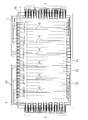
- FIG. 1 is a plan view schematically showing a main part of the display device
- FIG. 2 is an enlarged plan view schematically showing a configuration near a source terminal portion.
- the display device includes a horizontally long rectangular display panel 1 having a liquid crystal, and a central portion of the display panel 1 is a display area 2 for displaying a horizontally long rectangular image.
- the periphery of the display area 2 has a horizontally long rectangular frame shape, and is a non-display area 2b in which no video is displayed.
- a plurality of gate terminal portions 3, 3,..., 3 are arranged in parallel in the short side of the display panel 1 (the right side or the left side in FIG. 1).
- a scanning signal line (not shown) extends in the horizontal direction from each of the gate terminal portions 3.
- a plurality of data signal lines 5, 5,..., 5 extending in the vertical direction are arranged in parallel in the horizontal direction.
- the data signal lines 5 and the scanning signal lines are orthogonal to each other and arranged on the display panel 1 in a matrix.
- a thin film transistor (not shown) and a pixel electrode (not shown) connected to the thin film transistor are provided in the vicinity of the intersection of the data signal line 5 and the scanning signal line.
- the thin film transistor is ON / OFF controlled by the scanning signal line, a signal potential is applied from the data signal line 5 to each pixel electrode, the alignment state of the liquid crystal changes, and information is displayed.
- the display area 2 includes a plurality of (24 in this embodiment) display blocks 2a, 2a,.
- a data signal line 5 is provided for each display block 2a. In FIG. 1, the data signal line 5 is partially omitted.
- a source substrate 8 is provided outside the one long side (the upper side in FIG. 1) of the display panel 1.
- the source substrate 8 is located next to the display panel 1 and is located outside the non-display area 2b.
- a plurality of spare wirings 40 are arranged around the display panel 1, and the spare wirings 40 are provided outside the non-display area 2 b or the display panel 1.
- the spare wiring 40 is routed from the middle of one long side of the display panel 1 toward the short side along the long side, and further to the other long side (the lower side in FIG. 1) along the short side. Has been routed towards. On the short side, the spare wiring 40 is connected to the gate terminal portion 3.
- the spare wiring 40 is further routed along the other long side of the display panel 1 toward the center of the long side. Both end portions of the data signal line 5 are provided on both long sides of the display panel 1 so as to be connectable to the spare wiring 40.
- a plurality of (24 in the present embodiment) source terminal portions 4, 4,..., 4 are arranged in parallel in one long side of the display panel 1.
- Each of the source terminal portions 4 corresponds to each of the display blocks 2a, and corresponds to each of the data signal lines 5.
- the source terminal portion 4 includes a plurality of connection terminals 20, 20,.
- the plurality of connection terminals 20 include first to third connection terminals 21 to 23 and an amplifier connection terminal 27.
- the first to third connection terminals 21 to 23 are arranged in order, and the second connection terminal 22 is located between the first and third connection terminals 21 and 23.
- the amplifier connection terminal 27 is separated from the first to third connection terminals 21 to 23.
- the first connection terminal 21 functions as an amplifier connection terminal.
- the first relay line 31 and the second relay line 32 are provided in the non-display area 2b of the display panel 1.
- Each of the first relay line 31 and the second relay line 32 extends in the lateral direction across the four source terminal portions 4, 4, 4, and 4.
- the four source terminal portions 4 are referred to as first to fourth source terminal portions 11 to 14, respectively.
- the first to fourth source terminal portions 11 to 14 are arranged in order in the horizontal direction.
- the first relay line 31 is connected to the input side of the first connection terminal 21 and the amplifier connection terminal 27 in the first source terminal portion 11 and the third source terminal portion 13.
- the second relay line 32 is connected to the input side of the first connection terminal 21 and the amplifier connection terminal 27 in the second source terminal portion 12 and the fourth source terminal portion 14.
- One end of the data signal line 5 is orthogonal to the first relay line 31 and the second relay line 32 in plan view.
- the data signal line 5, the first relay line 31, and the second relay line 32 are stacked with an insulating film (not shown) interposed therebetween.
- the data signal line 5 and the first relay line 31 and the second relay line 32 are not electrically connected.
- the other long side portion of the display panel 1 is provided with two L-shaped relay lines orthogonal to the other end of the data signal line 5 and the spare wiring 40 in plan view.
- the relay line, the other end of the data signal line 5 and the spare wiring 40 are not electrically connected.
- Two spare wirings 40, 40 are assigned to the four display blocks 2a, 2a, 2a, 2a, and the two spare wirings 40 are mounted on the source substrate 8.
- the two spare wirings 40 are referred to as a first spare wiring 41 and a second spare wiring 42.
- the first spare wiring 41 and the second spare wiring 42 extend in the lateral direction on the source substrate 8.
- a COF 6 Chip On Film
- two amplifiers 7 and 7 are mounted on the COF 6. Note that although a plurality of COFs 6 are provided corresponding to the connection terminals 20, the COFs 6 are simplified in FIG. 2 for easy understanding.
- the input side of one amplifier 7 is connected to an amplifier connection terminal 27.
- the input side of the other amplifier 7 is connected to the first connection terminal 21.
- the output side of the amplifier 7 is connected to the first spare wiring 41. It is connected to the.
- a part of the first spare wiring 41 is connected to the second connection terminal 22 in the first source terminal portion 11 or the third source terminal portion 13, routed by the display panel 1, and further the third connection terminal. 23, routed outside the display panel 1, and returned to the source substrate 8.
- the output side of the amplifier 7 is connected to the second spare wiring. 42.
- a part of the second spare wiring 42 is connected to the second connection terminal 22 in the second source terminal portion 12 or the fourth source terminal portion 14, routed by the display panel 1, and further the third connection terminal. 23, routed outside the display panel 1, and returned to the source substrate 8.
- the source terminal portion 4 is formed on the display panel 1.
- the source substrate 8 is provided outside the display panel 1.
- the portion 40a of the spare wiring 40 provided in the source terminal portion 4 and the portion 40b of the spare wiring 40 provided in the source substrate 8 are made of substantially the same material (for example, copper).
- the film thickness of the portion 40a is thinner than the film thickness of the portion 40b. Therefore, the resistance value in the source terminal portion 4 is higher than the resistance value in the source substrate 8. In other words, the resistance of the spare wiring 40 in the display panel 1 is higher than the resistance of the spare wiring 40 outside the display panel 1.
- connection terminals 20 provided for backup are provided at both ends of the source terminal portion 4.
- the spare connection terminal 20 is used to connect the gate terminal portion 3 and the source terminal portion 4 described above by the spare wiring 40.
- the spare connection terminal 20 is used for the above purpose.
- the spare connection terminal 20 is not used for the above purpose and is in an empty state.
- These vacant connection terminals 20 are used as the second and third connection terminals 22 and 23, and the limited area of the display panel 1 is efficiently used.
- FIG. 3 is an enlarged plan view schematically showing a state where the data signal line 5 is connected to the second relay line 32 when the data signal line 5 corresponding to the fourth source terminal section 14 is cut.
- the double line indicates the cut location C
- the cross mark indicates the connection location K.
- a dot indicates a state in which a signal from the data signal line 5 is transmitted to the spare wiring 40.
- the display device is inspected whether or not the data signal line 5 is cut, and the display device is manufactured. In this inspection, for example, when it is found that the data signal line 5 corresponding to the fourth source terminal portion 14 is cut, one end of the data signal line 5 and the second relay line 32 are melt-connected. In addition, in the other long side portion of the display panel 1, laser beams are irradiated to the other end of the data signal line 5 and each intersection between the second spare wiring 42 and the relay line, thereby melt-connecting each intersection. Further, in the second source terminal portion 12, the connection between the first and second connection terminals 21 and 22 is disconnected.
- the signal of the data signal line 5 is input to both amplifiers 7 and 7 through the first connection terminal 21 and the amplifier connection terminal 27 and amplified. Is output.
- the signal output from the amplifier 7 is transmitted to the second auxiliary wiring 42, is transmitted to the other long side of the display panel 1 through the second connection terminal 22 and the third connection terminal 23, and the data signal line. 5 is input to the other end.
- the signal transmitted to the second auxiliary wiring 42 by disconnecting the connection between the first and second connection terminals 21 and 22 is connected to the second source terminal unit 12. 7 is not input to the output side. Therefore, damage to the amplifier 7 can be prevented.
- the data signal line 5 corresponding to the second source terminal portion 12 is cut, one end of the data signal line 5 and the second relay line 32 are melt-connected. On the other long side of the display panel 1, the other end of the data signal line 5 and the intersections of the second spare wiring 42 and the relay line are melt-connected. In the fourth source terminal section 14, the first and first The two connection terminals 21 and 22 are disconnected.
- the input side of the amplifier 7 is connected to the first connection terminal 21, and the output side of the amplifier 7 is connected to the spare wiring 40.
- a part of the spare wiring 40 is routed to the inside of the display panel 1 through the second connection terminal 22, and is routed to the outside of the display panel 1 through the third connection terminal 23.
- the resistance value of the source terminal portion 4 is higher than that of the spare wiring 40.
- the second connection terminal 22 and the third connection terminal 22 in the other source terminal section 4 corresponding to the other data signal line 5 are connected.
- the connection terminal 23 By disconnecting the connection terminal 23, a signal is input to one data signal line 5 and the amplifier 7 and the spare wiring 40 in the other source terminal section 4 are disconnected.
- the melt-connected portion Since one data signal line 5 is routed to the inside of the display panel 1 through the second connection terminal 22 and the third connection terminal 23 and then to the outside, the melt-connected portion The distance from the low-resistance spare wiring 40 can be shortened, and the resistance of the entire wiring after repair can be reduced.
- the configuration of the first embodiment may be partially changed as follows.
- the second connection terminal 22 and the third connection terminal 23 are connected to each of the source terminal portions 4 (see FIG. 2), and the second connection terminal 22 and the second connection terminal 23 are connected as necessary. 3 is disconnected (see FIG. 3).
- the second connection terminal 22 in one source terminal portion 4 and the vacant connection terminal of the other source terminal portion 4 located next to the one source terminal portion 4 (the amplifier connection terminal 27 in FIG. 2). May be connected to the right terminal).
- the cut portion is located between the source terminal portions 4 and 4 and is separated from the source terminal portion 4. Therefore, it is possible to prevent the source terminal portion 4 from being defective due to a residue or the like generated at the time of cutting.
- FIG. 4 is an enlarged plan view schematically showing the configuration near the source terminal portion 4.
- the first to fourth source terminal portions 11 to 14 include fourth and fifth connection terminals 24 and 25.
- the fourth and fifth connection terminals 24 and 25 are arranged next to the third connection terminal 23 in order.
- the source substrate 8 is provided with a first wiring 51 extending in the lateral direction across the first and third source terminal portions 11 and 13.
- the output sides of both amplifiers 7 connected to the third source terminal portion 13 and the fourth connection terminal 24 in the first source terminal portion 11 are connected via a first wiring 51.
- a part of the first wiring 51 is connected to the fourth connection terminal 24 in the first source terminal unit 11, is routed to the display panel 1 from the outside of the display panel 1, and is further connected to the fifth source terminal 11. Are connected to the connection terminal 25, routed to the outside of the display panel 1, and connected to the first auxiliary wiring 41.
- the source substrate 8 is provided with a second wiring 52 extending in the lateral direction across the second and fourth source terminal portions 12 and 14.
- the output sides of both amplifiers 7 connected to the fourth source terminal section 14 and the fourth connection terminal 24 in the second source terminal section 12 are connected via a second wiring 52.
- a part of the second wiring 52 is connected to the fourth connection terminal 24 in the second source terminal portion 12, is routed to the display panel 1 from the outside of the display panel 1, and is further connected to the fifth source terminal portion 12. Are connected to the connection terminal 25, routed outside the display panel 1, and connected to the second auxiliary wiring 42.
- spare connection terminals 20 are used as the second to fifth connection terminals 22 to 25, and the limited area of the display panel 1 is efficiently used.
- FIG. 5 shows that when the data signal lines 5 and 5 corresponding to the first and fourth source terminal portions 11 and 14 are disconnected, the data signal lines 5 and 5 are connected to the first relay line 31 and the second relay line. It is an enlarged plan view which briefly shows the state connected to 32 each.
- the display device is inspected whether or not the data signal line 5 is cut, and the display device is manufactured.
- the one end portion of the data signal line 5 and the first relay line 31 are melt-connected.
- laser beams are irradiated to the other end of the data signal line 5 and each intersection between the first spare wiring 41 and the relay line, thereby melt-connecting each intersection.
- the connection of the fourth and fifth connection terminals 24 and 25 is cut off.
- the data signal line 5 corresponding to the fourth source terminal portion 14 when it is found that the data signal line 5 corresponding to the fourth source terminal portion 14 is cut, one end of the data signal line 5 and the second relay line 32 are melt-connected.
- laser beams are irradiated to the other end of the data signal line 5 and each intersection between the second spare wiring 42 and the relay line, thereby melt-connecting each intersection.
- the connection of the second and third connection terminals 22 and 23 is disconnected.
- the display device and the manufacturing method of the display device according to the second embodiment for example, when the data signal line 5 corresponding to the first source terminal unit 11 and the first spare wiring 41 are connected, the first source terminal unit 11, the fourth and fifth connection terminals 24 and 25 are disconnected.
- the data signal line 5 corresponding to the fourth source terminal portion 14 and the second spare wiring 42 are connected, the second and third connection terminals 22 and 23 in the second source terminal portion 12 are disconnected.
- Locations where the first spare wiring 41, the second spare wiring 42, the first wiring 51 and the second wiring 52 are routed inside the display panel 1, that is, the second to fifth connection terminals 22 to 25 are used as the first and second sources.
- the terminals 11 and 12 can be concentrated. Since the portions to be cut concentrate, the manufacturing efficiency of the display device can be improved.
- FIG. 6 shows that when the data signal lines 5 and 5 corresponding to the first and fourth source terminal portions 11 and 14 are cut off, the data signal lines 5 and 5 are connected to the first relay line 31 and the second relay line. It is an enlarged plan view which briefly shows the state connected to 32 each.
- the configuration of the display device according to the third embodiment is the same as that of the second embodiment except for the signs described later.
- A1 and “A2” for identifying the first relay line 31 and the second relay line 32 are attached in the vicinity of the first relay line 31 and the second relay line 32, respectively.
- “1-A1” is connected to the connection portion between the second and third connection terminals 22 and 23 in the first source terminal portion 11, and the connection between the fourth and fifth connection terminals 24 and 25 in the first source terminal portion 11.
- “3-A1” is in the portion, and “2-A2” is in the connection portion of the second and third connection terminals 22 and 23 in the second source terminal portion 12, and the fourth and fifth in the second source terminal portion 12.
- “4-A2” is attached to the connection portions of the connection terminals 24 and 25.
- X-A1 indicates a portion connected to the first source terminal portion 11 and the first relay line 31.
- terminal 1” to “terminal 4” for identifying the first to fourth source terminal portions 11 to 14 may be attached to the first to fourth source terminal portions 11 to 14, respectively.
- the manufacturer can confirm the sign and easily recognize the part to be cut. Therefore, the manufacturing efficiency of the display device can be increased.
- FIG. 7 is an enlarged plan view schematically showing a configuration near the source terminal portion 4.
- the sixth connection terminal 26 is provided next to the third connection terminal 23.
- the output side of the amplifier 7 is connected to the second auxiliary wiring 42.
- a part of the second auxiliary wiring 42 is connected to the second connection terminal 22, routed by the display panel 1, further connected to the third connection terminal 23, and routed outside the display panel 1. .
- a part of the first spare wiring 41 is connected to the sixth connection terminal 26, routed to the display panel 1, and connected to the second spare wiring 42.
- spare connection terminals 20 are used as the second, third, and sixth connection terminals 22, 23, and 26, and the limited area of the display panel 1 is efficiently used.
- FIG. 8 shows that when the data signal lines 5 and 5 corresponding to the first and fourth source terminal portions 11 and 14 are disconnected, the data signal lines 5 and 5 are connected to the first relay line 31 and the second relay line. It is an enlarged plan view which briefly shows the state connected to 32 each.
- the display device is inspected whether or not the data signal line 5 is cut, and the display device is manufactured. In this inspection, for example, when it is found that the data signal line 5 corresponding to the first source terminal portion 11 is cut, the one end portion of the data signal line 5 and the first relay line 31 are melt-connected. Further, in the other long side portion of the display panel 1, laser beams are irradiated to the other end of the data signal line 5 and each intersection between the first spare wiring 41 and the relay line, thereby melt-connecting each intersection. In the first to third source terminal portions 11 to 13, the connection between the sixth connection terminal 26 and the second and third connection terminals 22 and 23 is cut off.
- the data signal line 5 corresponding to the fourth source terminal portion 14 when it is found that the data signal line 5 corresponding to the fourth source terminal portion 14 is cut, one end of the data signal line 5 and the second relay line 32 are melt-connected.
- laser beams are irradiated to the other end of the data signal line 5 and each intersection between the second spare wiring 42 and the relay line, thereby melt-connecting each intersection.
- the connection between the third connection terminal 23 and the second and sixth connection terminals 22 and 26 is cut off.
- the display device and the manufacturing method of the display device according to the fourth embodiment for example, when the signal line corresponding to the fourth source terminal portion 14 is connected to the second spare wiring 42, the first to third The connection between the source terminal portions 11 to 13 and the second spare wiring 42 is disconnected.
- the connection between the second to fourth source terminal portions 12 to 14 and the first spare wire 41 is disconnected.
- Embodiment 1 or 4 a sign may be provided as in Embodiment 3. Also in the second to fourth embodiments, as in the first embodiment, the resistance of the spare wiring in the display panel 1 is higher than the resistance of the spare wiring outside the display panel 1.
Landscapes
- Physics & Mathematics (AREA)
- Nonlinear Science (AREA)
- Engineering & Computer Science (AREA)
- Chemical & Material Sciences (AREA)
- Crystallography & Structural Chemistry (AREA)
- General Physics & Mathematics (AREA)
- Optics & Photonics (AREA)
- Microelectronics & Electronic Packaging (AREA)
- Mathematical Physics (AREA)
- Computer Hardware Design (AREA)
- Theoretical Computer Science (AREA)
- Devices For Indicating Variable Information By Combining Individual Elements (AREA)
Abstract
データ信号線及び予備配線における抵抗値を削減することができる表示装置及び表示装置の製造方法を提供する。 表示領域及び該表示領域の周囲に位置する非表示領域を有する表示パネルと、該表示パネルに設けられており、映像信号を伝達する信号線と、前記表示パネルの外側及び表示パネルの非表示領域に引き回されており、前記信号線に接続されるべき予備配線と、複数の接続端子と、第1の接続端子にその入力側が接続され、前記予備配線にその出力側が接続された増幅器とを備え、前記第1の接続端子を介して前記信号線から前記増幅器に信号を入力すべき表示装置であって、前記増幅器の出力側にて、前記予備配線の一部は第2の接続端子に接続され、前記表示パネルの外側から前記非表示領域に引き回されており、更に第3の接続端子に接続され、前記表示パネルの外側に引き回されていることを特徴とする表示装置。
Description
本発明は映像を表示する表示装置及び表示装置の製造方法に関する。
薄型の表示装置、例えば液晶表示装置は、設置面積に比べて表示面積が大きいことから一般に広く普及している。例えばアクティブマトリクス型の液晶表示装置では、複数のデータ信号線及び走査信号線がマトリクス状に配される。
両者の交点近傍に薄膜トランジスタと、該薄膜トランジスタにつながる画素電極とが設けられる。走査信号線によって薄膜トランジスタがON/OFF制御され、データ信号線から各画素電極に信号電位が与えられて、液晶の配向状態が変化し、情報が表示される。
近年では、表示品位のさらなる向上が求められており、データ信号線の線幅は10μm以下(たとえば、6μm)と非常に細くなっている。このため、製造工程で断線が発生しやすい。例えば、成膜時に塵埃を巻き込んだ場合や、エッチングの際にレジストマスクにピンホールが生じた場合に断線が生じる。
データ信号線に断線が生じた場合、その断線箇所以降の画素電極には正しい信号電位を書き込むことができなくなる。その結果、画面上に黒線(ノーマリーブラックモード)や輝線(ノーマリーホワイトモード)が現れる。
このような断線を修正する為に、例えばデータ信号線の信号入力側端部近傍からパネル外部基板等を通って該データ信号線の反対側の端部近傍(表示領域の下側)に至る予備配線を設ける。断線したデータ信号線における断線箇所以降の部分の端部(終端部)と、予備配線とをレーザ等を用いてメルト接続することによって、断線箇所以降の部分に信号が入力される。
データ信号線及び予備配線における抵抗値が大きい場合、予備配線を介して入力された信号出力に大きな損失が生じるおそれがある。従って、データ信号線及び予備配線における抵抗値は小さいことが望ましい。
本発明は斯かる事情に鑑みてなされたものであり、データ信号線及び予備配線における抵抗値を削減することができる表示装置及び表示装置の製造方法を提供することを目的とする。
本発明に係る表示装置は、表示領域及び該表示領域の周囲に位置する非表示領域を有する表示パネルと、該表示パネルに設けられており、映像信号を伝達する信号線と、前記表示パネルの外側及び表示パネルの非表示領域に引き回されており、前記信号線に接続されるべき予備配線と、複数の接続端子と、第1の接続端子にその入力側が接続され、前記予備配線にその出力側が接続された増幅器とを備え、前記第1の接続端子を介して前記信号線から前記増幅器に信号を入力すべき表示装置であって、前記増幅器の出力側にて、前記予備配線の一部は第2の接続端子に接続され、前記表示パネルの外側から前記非表示領域に引き回されており、更に第3の接続端子に接続され、前記表示パネルの外側に引き回されていることを特徴とする。
本発明に係る表示装置は、前記表示パネルの周囲に設けられた配線と、前記表示パネルに設けられており、映像信号を伝達する第2信号線と、前記表示パネルに設けられており、前記配線及び第2信号線を接続すべき接続部と、該接続部にその入力側が接続され、前記配線にその出力側が接続された第2増幅器とを備え、前記配線の一部は前記第4の接続端子に接続され、前記表示パネルの外側から前記非表示領域に引き回されており、更に前記第5の接続端子に接続され、前記表示パネルの外側に引き回され、前記予備配線に接続されていることを特徴とする。
本発明に係る表示装置は、前記第2及び第3の接続端子と、前記第4及び第5の接続端子とを識別する標識を備えることを特徴とする。
本発明に係る表示装置は、前記表示パネルの周囲に設けられた第2予備配線を備え、前記第2の接続端子に接続され、前記表示パネルの外側から前記非表示領域に引き回された前記予備配線は更に第6の接続端子に接続され、前記表示パネルの外側に引き回され、前記第2予備配線に接続されていることを特徴とする。
本発明に係る表示装置は、前記表示パネルの外側に前記予備配線を有する基板が設けられていることを特徴とする。
本発明に係る表示装置の製造方法は、表示領域及び該表示領域の周囲に位置する非表示領域を有する表示パネルと、該表示パネルに設けられており、映像信号を伝達する複数の信号線と、前記表示パネルの外側及び表示パネルの非表示領域に引き回されており、前記信号線に接続されるべき予備配線と、前記複数の信号線夫々に対応しており、複数の接続端子を有する複数の接続部と、該接続部夫々に対応しており、第1の接続端子にその入力側が接続され、前記予備配線にその出力側が接続された増幅器とを備え、前記第1の接続端子を介して前記信号線から前記増幅器に信号を入力するように構成されており、予め前記予備配線の一部は第2の接続端子に接続され、前記表示パネルの外側から前記非表示領域に引き回されており、更に第3の接続端子に接続され、前記表示パネルの外側に引き回されている表示装置の製造方法であって、前記複数の信号線夫々の切断の有無を検査する工程と、該工程にて切断が検出された一の前記信号線及び該一の信号線に対応する前記接続部の第1の接続端子を接続させる工程と、他の信号線に対応する前記接続部の第2の接続端子を切断する工程とを備えることを特徴とする。
表示パネルの一側において、予備配線は表示パネルの外側に設けられている。予備配線に接続可能な複数の信号線が表示パネルに設けられている。また複数の信号線夫々に対応する接続部が設けられている。接続部と予備配線との間には、複数の接続端子を有する増幅器が設けられている。本発明においては増幅器の入力側を第1の接続端子に接続し、増幅器の出力側を予備配線に接続する。予備配線の一部は第2の接続端子を介して表示パネルに引き回され、第3の接続端子を介して表示パネルの外側に引き回されている。断線した一の信号線と予備配線とをレーザ等を用いてメルト接続した場合に、他の信号線に対応する他の接続部における第2の接続端子及び第3の接続端子を切断することによって、一の信号線に信号を入力し且つ他の接続部における増幅器と前記予備配線とを切断する。
本発明においては、配線と、第2信号線と、第2接続部と、第2増幅器とを備える。第2増幅器の入力側は第2接続部に接続され、出力側は配線に接続されている。第2信号線は第2接続部に接続される。配線の一部は、前記接続部の第4の接続端子に接続されて、前記表示パネルに引き回され、第5の接続端子に接続されて、前記表示パネルの外側に引き回され、前記予備配線に接続されている。信号線と予備配線とを接続した場合、第4及び第5の接続端子を切断する。第2信号線と予備配線とを接続した場合、第2及び第3の接続端子を切断する。予備配線及び配線を表示パネルの内側に引き回す箇所、すなわち第2~第5の接続端子を接続部に集中させることができる。
本発明においては、製造者は標識を確認し、切断すべき箇所を認識する。
本発明においては、一の信号線が予備配線に接続された場合に、他の信号線に対応する接続部と前記予備配線との接続を切断する。また一の信号線が第2予備配線に接続された場合に、他の信号線に対応する接続部と第2予備配線との接続を切断する。
本発明においては、予備配線を基板に設けることによって、予備配線の抵抗値を接続部よりも小さくすることを実現する。
本発明に係る表示装置及び表示装置の製造方法にあっては、増幅器の入力側を第1の接続端子に接続し、増幅器の出力側を予備配線に接続する。予備配線の一部は第2の接続端子を介して表示パネルに引き回され、第3の接続端子を介して表示パネルの外側に引き回されている。断線した一の信号線と予備配線とをレーザ等を用いてメルト接続した場合に、他の信号線に対応する他の接続部における第2の接続端子及び第3の接続端子を切断することによって、一の信号線に信号を入力し且つ他の接続部における増幅器と前記予備配線とを切断する。一の信号線のメルト接続した箇所から予備配線までの距離を短くし、補修後の配線全体の抵抗を低減させることができる。
(実施の形態1)
以下本発明を実施の形態1に係る表示装置を示す図面に基づいて説明する。図1は表示装置の要部を略示する平面図、図2はソース端子部付近の構成を略示する拡大平面図である。
以下本発明を実施の形態1に係る表示装置を示す図面に基づいて説明する。図1は表示装置の要部を略示する平面図、図2はソース端子部付近の構成を略示する拡大平面図である。
表示装置は、液晶を有する横長矩形の表示パネル1を備え、表示パネル1の中央部は、横長矩形の映像を表示する表示領域2になっている。表示パネル1において、表示領域2の周囲は、横長矩形の額縁形をなし、映像が表示されない非表示領域2bとなっている。表示パネル1の短辺夫々(図1における右辺又は左辺)には、複数のゲート端子部3、3、・・・、3が縦向きに並設されている。該ゲート端子部3夫々から、走査信号線(図示略)が横方向に延びている。表示領域2には、縦方向に延びた複数のデータ信号線5、5、・・・、5が横方向に並設されている。データ信号線5及び走査信号線は直交しており、表示パネル1にマトリクス状に配されている。
データ信号線5及び走査信号線の交点近傍に薄膜トランジスタ(図示略)と、該薄膜トランジスタにつながる画素電極(図示略)とが設けられている。走査信号線によって薄膜トランジスタがON/OFF制御され、データ信号線5から各画素電極に信号電位が与えられて、液晶の配向状態が変化し、情報が表示される。
表示領域2は、縦割りにされた複数(本実施例においては24個)の表示ブロック2a、2a、・・・2aを有する。表示ブロック2a夫々にデータ信号線5が設けられている。なお図1において、データ信号線5の記載を一部省略している。
図2に示すように、表示パネル1の一方の長辺(図1における上辺)の外側には、ソース基板8が設けられている。ソース基板8は表示パネル1の隣に位置し、非表示領域2bの外側に位置する。
表示パネル1の周囲に複数の予備配線40が配置されており、予備配線40は非表示領域2b又は表示パネル1の外側に設けられている。予備配線40は、表示パネル1の一方の長辺の中途部から、該長辺に沿って短辺に向けて引き回され、更に短辺に沿って他方の長辺(図1における下辺)に向けて引き回されている。短辺においては、予備配線40はゲート端子部3に接続されている。予備配線40は更に表示パネル1の他方の長辺に沿って、該長辺の中央部に向けて引き回されている。データ信号線5の両端部はそれぞれ、表示パネル1の両長辺において、予備配線40に接続可能に設けられている。
非表示領域2bにおいて、表示パネル1の一方の長辺には複数(本実施例においては24個)のソース端子部4、4、・・・、4が横方向に並設されている。ソース端子部4夫々は表示ブロック2a夫々に対応しており、データ信号線5夫々に対応している。ソース端子部4は、横方向に並設された複数の接続端子20、20、・・・、20を備える。
複数の接続端子20は第1~第3の接続端子21~23及び増幅器接続端子27を含む。第1~第3の接続端子21~23は順に並んでおり、第2の接続端子22は第1及び第3の接続端子21、23の間に位置する。増幅器接続端子27は第1~第3の接続端子21~23から離間している。なお第1の接続端子21は増幅器接続端子として機能している。
ソース端子部4及び表示ブロック2aの間において、第1中継線31及び第2中継線32が表示パネル1の非表示領域2bに設けられている。第1中継線31及び第2中継線32夫々は四つのソース端子部4、4、4、4に亘って横方向に延びている。以下四つのソース端子部4夫々を第1~第4ソース端子部11~14と称する。第1~第4ソース端子部11~14は横方向に順に並んでいる。
第1中継線31は第1ソース端子部11及び第3ソース端子部13において、第1の接続端子21及び増幅器接続端子27の入力側に接続している。第2中継線32は第2ソース端子部12及び第4ソース端子部14において、第1の接続端子21及び増幅器接続端子27の入力側に接続している。
データ信号線5の一端部は、平面視において第1中継線31及び第2中継線32に直交している。データ信号線5と第1中継線31及び第2中継線32とは絶縁膜(図示略)を介して積層している。換言すれば、データ信号線5と第1中継線31及び第2中継線32とは電気的に接続されていない。データ信号線5の一端部と第1中継線31又は第2中継線32との交点にレーザを照射することによって、両者をメルト接続することができる。
なお表示パネル1の他方の長辺部分には、平面視においてデータ信号線5の他端部及び予備配線40に直交するL形の二つの中継線が設けられている。中継線とデータ信号線5の他端部及び予備配線40とは、電気的に接続されていない。データ信号線5の他端部及び予備配線40と中継線との交点夫々にレーザを照射することによって、交点夫々をメルト接続させることができる。
四つの表示ブロック2a、2a、2a、2aに対して二つの予備配線40、40が割り当てられており、該二つの予備配線40はソース基板8に実装されている。以下二つの予備配線40を第1予備配線41及び第2予備配線42と称する。第1予備配線41及び第2予備配線42はソース基板8にて横方向に延びている。
表示パネル1及びソース基板8の間にCOF6(Chip On Film)が設けられており、該COF6に二つの増幅器7、7が実装されている。なおCOF6は接続端子20に対応して複数設けられているが、理解を容易にする為に、図2において、COF6は簡略化して記載されている。一方の増幅器7の入力側は増幅器接続端子27に接続されている。他方の増幅器7の入力側は第1の接続端子21に接続されている。
第1ソース端子部11又は第3ソース端子部13において、増幅器7の入力側が第1の接続端子21又は増幅器接続端子27に接続されている場合、増幅器7の出力側は、第1予備配線41に接続されている。第1予備配線41の一部は、第1ソース端子部11又は第3ソース端子部13において、第2の接続端子22に接続され、表示パネル1にて引き回され、更に第3の接続端子23に接続され、表示パネル1の外側に引き回され、ソース基板8に戻される。
第2ソース端子部12又は第4ソース端子部14において、増幅器7の入力側が第1の接続端子21又は増幅器接続端子27に接続されている場合、前記増幅器7の出力側は、第2予備配線42に接続されている。第2予備配線42の一部は、第2ソース端子部12又は第4ソース端子部14において、第2の接続端子22に接続され、表示パネル1にて引き回され、更に第3の接続端子23に接続され、表示パネル1の外側に引き回され、ソース基板8に戻される。
ソース端子部4は表示パネル1に形成されている。ソース基板8は表示パネル1の外側に設けられている。ソース端子部4に設けられている予備配線40の部分40aと、ソース基板8に設けられた予備配線40の部分40bとは略同じ材料(例えば銅)によって構成されている。部分40aの膜厚は部分40bの膜厚よりも薄い。そのため、ソース端子部4における抵抗値はソース基板8における抵抗値よりも高い。換言すれば、表示パネル1における予備配線40の抵抗は、表示パネル1の外側における予備配線40の抵抗よりも高い。
ソース端子部4の両端部夫々には、予備用に設けられた所定数(例えば6個)の接続端子20が設けられている。予備用の接続端子20は、前述したゲート端子部3及びソース端子部4間を予備配線40によって接続させる為に使用される。ソース端子部4が表示パネル1の長辺の端部に位置している場合、予備用の接続端子20は、上記目的の為に使用される。しかし、ソース端子部4が前記長辺の中途部に位置している場合、予備用の接続端子20は上記目的の為に使用されず、空いた状態となる。これらの空いた接続端子20を第2及び第3の接続端子22、23として使用しており、限られた表示パネル1の領域を効率良く使用している。
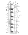
図3は第4ソース端子部14に対応するデータ信号線5が切断されている場合に、データ信号線5を第2中継線32に接続した状態を略示する拡大平面図である。なお図3において、二重線は切断箇所Cを示し、クロスマークは接続箇所Kを示す。またドットはデータ信号線5からの信号が予備配線40に伝達されている状態を示す。
表示装置に対して、データ信号線5が切断されているか否かの検査が行われ、表示装置が製造される。この検査において、例えば第4ソース端子部14に対応するデータ信号線5が切断されていることが判明した場合、前記データ信号線5の一端部と第2中継線32とをメルト接続する。また表示パネル1の他方の長辺部分において、データ信号線5の他端部及び第2予備配線42と中継線との交点夫々にレーザを照射することによって、交点夫々をメルト接続する。また第2ソース端子部12において、第1及び第2の接続端子21、22の接続を切断する。
データ信号線5と第2中継線32とを接続することによって、データ信号線5の信号は、第1の接続端子21及び増幅器接続端子27を通って両増幅器7、7に入力され、増幅されて、出力される。増幅器7から出力された信号は第2予備配線42を伝達し、第2の接続端子22及び第3の接続端子23を経由し、表示パネル1の他方の長辺側に伝達され、データ信号線5の他端部に入力される。
第2ソース端子部12において、第1及び第2の接続端子21、22の接続を切断することによって、第2予備配線42に伝達された信号は、第2ソース端子部12に接続された増幅器7の出力側に入力されない。そのため、前記増幅器7の破損を防止することができる。
なお第2ソース端子部12に対応するデータ信号線5が切断されている場合には、該データ信号線5の一端部と第2中継線32とがメルト接続される。また表示パネル1の他方の長辺側において、データ信号線5の他端部及び第2予備配線42と中継線との交点夫々がメルト接続され、第4ソース端子部14において、第1及び第2の接続端子21、22の接続が切断される。
第1ソース端子部11に対応するデータ信号線5が切断されている場合には、該データ信号線5の一端部と第1中継線31とがメルト接続される。また表示パネル1の他方の長辺側において、データ信号線5の他端部及び第1予備配線41と中継線との交点夫々がメルト接続され、第3ソース端子部13において、第1及び第2の接続端子21、22の接続が切断される。
第3ソース端子部13に対応するデータ信号線5が切断されている場合には、該データ信号線5の一端部と第1中継線31とがメルト接続される。また表示パネル1の他方の長辺側において、データ信号線5の他端部及び第1予備配線41と中継線との交点夫々がメルト接続され、第1ソース端子部11において、第1及び第2の接続端子21、22の接続が切断される。
実施の形態1に係る表示装置及び表示装置の製造方法にあっては、増幅器7の入力側を第1の接続端子21に接続し、増幅器7の出力側を予備配線40に接続する。予備配線40の一部は第2の接続端子22を介して表示パネル1の内側に引き回され、第3の接続端子23を介して表示パネル1の外側に引き回されている。ソース端子部4の抵抗値は予備配線40よりも高い。
断線した一のデータ信号線5と予備配線40とをレーザ等を用いてメルト接続した場合に、他のデータ信号線5に対応する他のソース端子部4における第2の接続端子22及び第3の接続端子23を切断することによって、一のデータ信号線5に信号を入力し且つ他のソース端子部4における増幅器7と前記予備配線40とを切断する。
一のデータ信号線5は、第2の接続端子22及び第3の接続端子23を介して、表示パネル1の内側に引き回された後、外側に引き回されているので、メルト接続した箇所から抵抗値の低い予備配線40までの距離を短くし、補修後の配線全体の抵抗を低減させることができる。
(変形例)
なお実施の形態1の構成を以下のように一部変更してもよい。実施の形態1においては、ソース端子部4それぞれにおいて、第2の接続端子22及び第3の接続端子23が接続されており(図2参照)、必要に応じて第2の接続端子22及び第3の接続端子23間の接続を切断する(図3参照)。これに対し、一のソース端子部4における第2の接続端子22と、該一のソース端子部4の隣に位置する他のソース端子部4の空いた接続端子(図2の増幅器接続端子27の右側の端子)とを接続してもよい。この場合、切断箇所が両ソース端子部4、4の間に位置し、ソース端子部4から離れる。そのため、切断時に生じる残渣等によって、ソース端子部4に不具合が発生することを防止することができる。
なお実施の形態1の構成を以下のように一部変更してもよい。実施の形態1においては、ソース端子部4それぞれにおいて、第2の接続端子22及び第3の接続端子23が接続されており(図2参照)、必要に応じて第2の接続端子22及び第3の接続端子23間の接続を切断する(図3参照)。これに対し、一のソース端子部4における第2の接続端子22と、該一のソース端子部4の隣に位置する他のソース端子部4の空いた接続端子(図2の増幅器接続端子27の右側の端子)とを接続してもよい。この場合、切断箇所が両ソース端子部4、4の間に位置し、ソース端子部4から離れる。そのため、切断時に生じる残渣等によって、ソース端子部4に不具合が発生することを防止することができる。
(実施の形態2)
以下本発明を実施の形態2に係る表示装置を示す図面に基づいて説明する。図4はソース端子部4付近の構成を略示する拡大平面図である。
以下本発明を実施の形態2に係る表示装置を示す図面に基づいて説明する。図4はソース端子部4付近の構成を略示する拡大平面図である。
第1~第4ソース端子部11~14は、第4及び第5の接続端子24、25を備える。第4及び第5の接続端子24、25は第3の接続端子23の隣に順に並んでいる。ソース基板8には、第1及び第3ソース端子部11、13に亘って横方向に延びた第1配線51が設けられている。第3ソース端子部13に接続された両増幅器7の出力側と第1ソース端子部11における第4の接続端子24とは、第1配線51を介して接続されている。
第1配線51の一部は、第1ソース端子部11における第4の接続端子24に接続され、表示パネル1の外側から表示パネル1に引き回され、更に第1ソース端子部11における第5の接続端子25に接続され、表示パネル1の外側に引き回されて、第1予備配線41に接続されている。
ソース基板8には、第2及び第4ソース端子部12、14に亘って横方向に延びた第2配線52が設けられている。第4ソース端子部14に接続された両増幅器7の出力側と第2ソース端子部12における第4の接続端子24とは、第2配線52を介して接続されている。
第2配線52の一部は、第2ソース端子部12における第4の接続端子24に接続され、表示パネル1の外側から表示パネル1に引き回され、更に第2ソース端子部12における第5の接続端子25に接続され、表示パネル1の外側に引き回されて、第2予備配線42に接続されている。
なお予備用の空いた接続端子20を第2~第5の接続端子22~25として使用しており、限られた表示パネル1の領域を効率良く使用している。
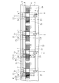
図5は第1及び第4ソース端子部11、14に対応するデータ信号線5、5夫々が切断されている場合に、前記データ信号線5、5を第1中継線31及び第2中継線32夫々に接続した状態を略示する拡大平面図である。
表示装置に対して、データ信号線5が切断されているか否かの検査が行われ、表示装置が製造される。この検査において、例えば第1ソース端子部11に対応するデータ信号線5が切断されていることが判明した場合、前記データ信号線5の一端部と第1中継線31とをメルト接続する。また表示パネル1の他方の長辺部分において、データ信号線5の他端部及び第1予備配線41と中継線との交点夫々にレーザを照射することによって、交点夫々をメルト接続する。また第1ソース端子部11において、第4及び第5の接続端子24、25の接続を切断する。
例えば第4ソース端子部14に対応するデータ信号線5が切断されていることが判明した場合、前記データ信号線5の一端部と第2中継線32とをメルト接続する。また表示パネル1の他方の長辺部分において、データ信号線5の他端部及び第2予備配線42と中継線との交点夫々にレーザを照射することによって、交点夫々をメルト接続する。また第2ソース端子部12において、第2及び第3の接続端子22、23の接続を切断する。
実施の形態2に係る表示装置及び表示装置の製造方法にあっては、例えば第1ソース端子部11に対応するデータ信号線5と第1予備配線41とを接続した場合、第1ソース端子部11における第4及び第5の接続端子24、25を切断する。第4ソース端子部14に対応するデータ信号線5と第2予備配線42とを接続した場合、第2ソース端子部12における第2及び第3の接続端子22、23を切断する。第1予備配線41、第2予備配線42、第1配線51及び第2配線52を表示パネル1の内側に引き回す箇所、すなわち第2~第5の接続端子22~25を第1及び第2ソース端子部11、12に集中させることができる。切断される箇所が集中するので、表示装置の製造効率を向上させることができる。
実施の形態2に係る構成の内、実施の形態1と同様な構成については同じ符号を付し、その詳細な説明を省略する。
(実施の形態3)
以下本発明を実施の形態3に係る表示装置を示す図面に基づいて説明する。図6は第1及び第4ソース端子部11、14に対応するデータ信号線5、5夫々が切断されている場合に、前記データ信号線5、5を第1中継線31及び第2中継線32夫々に接続した状態を略示する拡大平面図である。なお後述する標識を除き、実施の形態3に係る表示装置の構成は実施の形態2と同じである。
以下本発明を実施の形態3に係る表示装置を示す図面に基づいて説明する。図6は第1及び第4ソース端子部11、14に対応するデータ信号線5、5夫々が切断されている場合に、前記データ信号線5、5を第1中継線31及び第2中継線32夫々に接続した状態を略示する拡大平面図である。なお後述する標識を除き、実施の形態3に係る表示装置の構成は実施の形態2と同じである。
また第1中継線31及び第2中継線32夫々の近傍に、第1中継線31及び第2中継線32を識別する「A1」及び「A2」が夫々付されている。
また第1ソース端子部11における第2及び第3の接続端子22、23の接続部分に「1-A1」が、第1ソース端子部11における第4及び第5の接続端子24、25の接続部分に「3-A1」が、第2ソース端子部12における第2及び第3の接続端子22、23の接続部分に「2-A2」が、第2ソース端子部12における第4及び第5の接続端子24、25の接続部分に「4-A2」が付されている。
上記「X-AY」(X=1~4、Y=1又は2)形式の標識は、第Xソース端子部及び第Y中継線に接続されている部分を示す。例えば、「1-A1」は、第1ソース端子部11及び第1中継線31に接続されている部分を示す。なお第1~第4ソース端子部11~14に、第1~第4ソース端子部11~14を識別する「端子1」~「端子4」を夫々付してもよい。
実施の形態3に係る表示装置及び表示装置の製造方法にあっては、標識を設けることによって、製造者は標識を確認し、切断すべき箇所を容易に認識することができる。そのため表示装置の製造効率を高めることができる。
(実施の形態4)
以下本発明を実施の形態4に係る表示装置を示す図面に基づいて説明する。図7はソース端子部4付近の構成を略示する拡大平面図である。
以下本発明を実施の形態4に係る表示装置を示す図面に基づいて説明する。図7はソース端子部4付近の構成を略示する拡大平面図である。
第1~第4ソース端子部11~14において、第6の接続端子26が第3の接続端子23の隣に設けられている。増幅器7の出力側は第2予備配線42に接続されている。第2予備配線42の一部は第2の接続端子22に接続され、表示パネル1にて引き回され、更に第3の接続端子23に接続され、表示パネル1の外側に引き回されている。また第1予備配線41の一部は第6の接続端子26に接続され、表示パネル1に引き回され、第2予備配線42に接続されている。
なお予備用の空いた接続端子20を第2、第3及び第6の接続端子22、23、26として使用しており、限られた表示パネル1の領域を効率良く使用している。
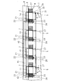
図8は第1及び第4ソース端子部11、14に対応するデータ信号線5、5夫々が切断されている場合に、前記データ信号線5、5を第1中継線31及び第2中継線32夫々に接続した状態を略示する拡大平面図である。
表示装置に対して、データ信号線5が切断されているか否かの検査が行われ、表示装置が製造される。この検査において、例えば第1ソース端子部11に対応するデータ信号線5が切断されていることが判明した場合、前記データ信号線5の一端部と第1中継線31とをメルト接続する。また表示パネル1の他方の長辺部分において、データ信号線5の他端部及び第1予備配線41と中継線との交点夫々にレーザを照射することによって、交点夫々をメルト接続する。また第1~第3ソース端子部11~13において、第6の接続端子26と第2及び第3の接続端子22、23の接続を切断する。
例えば第4ソース端子部14に対応するデータ信号線5が切断されていることが判明した場合、前記データ信号線5の一端部と第2中継線32とをメルト接続する。また表示パネル1の他方の長辺部分において、データ信号線5の他端部及び第2予備配線42と中継線との交点夫々にレーザを照射することによって、交点夫々をメルト接続する。また第1~第3ソース端子部11~13において、第3の接続端子23と第2及び第6の接続端子22、26の接続を切断する。
実施の形態4に係る表示装置及び表示装置の製造方法にあっては、例えば、第4ソース端子部14に対応する信号線が第2予備配線42に接続された場合に、第1~第3ソース端子部11~13と第2予備配線42との接続を切断する。
また例えば、第1ソース端子部11に対応する信号線が第1予備配線41に接続された場合に、第2~第4ソース端子部12~14と第1予備配線41との接続を切断する。
実施の形態4に係る構成の内、実施の形態1~3と同様な構成については同じ符号を付し、その詳細な説明を省略する。
なお実施の形態1又は4において、実施の形態3と同様に標識を設けてもよい。また実施の形態2~4においても、実施の形態1と同様に、表示パネル1における予備配線の抵抗は、表示パネル1の外側における予備配線の抵抗よりも高い。
今回開示した実施の形態は、全ての点で例示であって、制限的なものではないと考えられるべきである。各実施例にて記載されている技術的特徴は互いに組み合わせることができ、本発明の範囲は、請求の範囲内での全ての変更及び請求の範囲と均等の範囲が含まれることが意図される。
1 表示パネル
4 ソース端子部(接続部)
5 データ信号線(信号線)
7 増幅器
8 ソース基板(基板)
20 接続端子
21 第1の接続端子
22 第2の接続端子
23 第3の接続端子
24 第4の接続端子
25 第5の接続端子
26 第6の接続端子
40 予備配線
41 第1予備配線
42 第2予備配線
51 第1配線(配線)
52 第2配線(配線)
4 ソース端子部(接続部)
5 データ信号線(信号線)
7 増幅器
8 ソース基板(基板)
20 接続端子
21 第1の接続端子
22 第2の接続端子
23 第3の接続端子
24 第4の接続端子
25 第5の接続端子
26 第6の接続端子
40 予備配線
41 第1予備配線
42 第2予備配線
51 第1配線(配線)
52 第2配線(配線)
Claims (6)
- 表示領域及び該表示領域の周囲に位置する非表示領域を有する表示パネルと、該表示パネルに設けられており、映像信号を伝達する信号線と、前記表示パネルの外側及び表示パネルの非表示領域に引き回されており、前記信号線に接続されるべき予備配線と、複数の接続端子と、第1の接続端子にその入力側が接続され、前記予備配線にその出力側が接続された増幅器とを備え、前記第1の接続端子を介して前記信号線から前記増幅器に信号を入力すべき表示装置であって、
前記増幅器の出力側にて、前記予備配線の一部は第2の接続端子に接続され、前記表示パネルの外側から前記非表示領域に引き回されており、更に第3の接続端子に接続され、前記表示パネルの外側に引き回されていること
を特徴とする表示装置。 - 前記表示パネルの周囲に設けられた配線と、
前記表示パネルに設けられており、映像信号を伝達する第2信号線と、
前記表示パネルに設けられており、前記配線及び第2信号線を接続すべき接続部と、
該接続部にその入力側が接続され、前記配線にその出力側が接続された第2増幅器と
を備え、
前記配線の一部は前記第4の接続端子に接続され、前記表示パネルの外側から前記非表示領域に引き回されており、更に前記第5の接続端子に接続され、前記表示パネルの外側に引き回され、前記予備配線に接続されていること
を特徴とする請求項1に記載の表示装置。 - 前記第2及び第3の接続端子と、前記第4及び第5の接続端子とを識別する標識を備えること
を特徴とする請求項2に記載の表示装置。 - 前記表示パネルの周囲に設けられた第2予備配線を備え、
前記第2の接続端子に接続され、前記表示パネルの外側から前記非表示領域に引き回された前記予備配線は更に第6の接続端子に接続され、前記表示パネルの外側に引き回され、前記第2予備配線に接続されていることを特徴とする請求項1に記載の表示装置。 - 前記表示パネルの外側に前記予備配線を有する基板が設けられていること
を特徴とする請求項1から4のいずれか一つに記載の表示装置。 - 表示領域及び該表示領域の周囲に位置する非表示領域を有する表示パネルと、該表示パネルに設けられており、映像信号を伝達する複数の信号線と、前記表示パネルの外側及び表示パネルの非表示領域に引き回されており、前記信号線に接続されるべき予備配線と、前記複数の信号線夫々に対応しており、複数の接続端子を有する複数の接続部と、該接続部夫々に対応しており、第1の接続端子にその入力側が接続され、前記予備配線にその出力側が接続された増幅器とを備え、前記第1の接続端子を介して前記信号線から前記増幅器に信号を入力するように構成されており、予め前記予備配線の一部は第2の接続端子に接続され、前記表示パネルの外側から前記非表示領域に引き回されており、更に第3の接続端子に接続され、前記表示パネルの外側に引き回されている表示装置の製造方法であって、
前記複数の信号線夫々の切断の有無を検査する工程と、
該工程にて切断が検出された一の前記信号線及び該一の信号線に対応する前記接続部の第1の接続端子を接続させる工程と、
他の信号線に対応する前記接続部の第2の接続端子を切断する工程と
を備えることを特徴とする表示装置の製造方法。
Priority Applications (2)
| Application Number | Priority Date | Filing Date | Title |
|---|---|---|---|
| US15/536,476 US10303024B2 (en) | 2014-12-26 | 2014-12-26 | Display apparatus and method of manufacturing display apparatus |
| PCT/JP2014/084596 WO2016103475A1 (ja) | 2014-12-26 | 2014-12-26 | 表示装置及び表示装置の製造方法 |
Applications Claiming Priority (1)
| Application Number | Priority Date | Filing Date | Title |
|---|---|---|---|
| PCT/JP2014/084596 WO2016103475A1 (ja) | 2014-12-26 | 2014-12-26 | 表示装置及び表示装置の製造方法 |
Publications (1)
| Publication Number | Publication Date |
|---|---|
| WO2016103475A1 true WO2016103475A1 (ja) | 2016-06-30 |
Family
ID=56149560
Family Applications (1)
| Application Number | Title | Priority Date | Filing Date |
|---|---|---|---|
| PCT/JP2014/084596 Ceased WO2016103475A1 (ja) | 2014-12-26 | 2014-12-26 | 表示装置及び表示装置の製造方法 |
Country Status (2)
| Country | Link |
|---|---|
| US (1) | US10303024B2 (ja) |
| WO (1) | WO2016103475A1 (ja) |
Families Citing this family (1)
| Publication number | Priority date | Publication date | Assignee | Title |
|---|---|---|---|---|
| US11366367B2 (en) * | 2020-08-21 | 2022-06-21 | Sharp Kabushiki Kaisha | Display device and inspection method of display device |
Citations (3)
| Publication number | Priority date | Publication date | Assignee | Title |
|---|---|---|---|---|
| JP2004004492A (ja) * | 2002-03-25 | 2004-01-08 | Sharp Corp | 配線基板の接続構造、および表示装置 |
| WO2007020784A1 (ja) * | 2005-08-12 | 2007-02-22 | Sharp Kabushiki Kaisha | 表示装置、液晶表示装置および表示装置の製造方法 |
| WO2013011855A1 (ja) * | 2011-07-15 | 2013-01-24 | シャープ株式会社 | アクティブマトリクス型表示装置 |
Family Cites Families (1)
| Publication number | Priority date | Publication date | Assignee | Title |
|---|---|---|---|---|
| JP5770266B2 (ja) * | 2011-04-08 | 2015-08-26 | シャープ株式会社 | 表示装置 |
-
2014
- 2014-12-26 US US15/536,476 patent/US10303024B2/en not_active Expired - Fee Related
- 2014-12-26 WO PCT/JP2014/084596 patent/WO2016103475A1/ja not_active Ceased
Patent Citations (3)
| Publication number | Priority date | Publication date | Assignee | Title |
|---|---|---|---|---|
| JP2004004492A (ja) * | 2002-03-25 | 2004-01-08 | Sharp Corp | 配線基板の接続構造、および表示装置 |
| WO2007020784A1 (ja) * | 2005-08-12 | 2007-02-22 | Sharp Kabushiki Kaisha | 表示装置、液晶表示装置および表示装置の製造方法 |
| WO2013011855A1 (ja) * | 2011-07-15 | 2013-01-24 | シャープ株式会社 | アクティブマトリクス型表示装置 |
Also Published As
| Publication number | Publication date |
|---|---|
| US20170351151A1 (en) | 2017-12-07 |
| US10303024B2 (en) | 2019-05-28 |
Similar Documents
| Publication | Publication Date | Title |
|---|---|---|
| JP6328794B2 (ja) | 表示装置及び表示装置の製造方法 | |
| KR100372300B1 (ko) | 수리선을 가지는 액정 표시 장치용 박막 트랜지스터 기판 | |
| US7649580B2 (en) | Liquid crystal display panel and repairing method thereof | |
| CN104461147B (zh) | 显示面板及其修复方法 | |
| US20210257267A1 (en) | Display panel and method for manufacturing same | |
| US9983450B2 (en) | GOA circuit module, method for testing the same, display panel and display apparatus | |
| US10159145B2 (en) | Circuit device and display apparatus | |
| CN101950110A (zh) | 显示面板 | |
| CN107656386A (zh) | 阵列基板及修复方法和显示面板 | |
| TW201638920A (zh) | 電子紙顯示裝置及其製作方法 | |
| JP4567058B2 (ja) | 表示装置、液晶表示装置および表示装置の製造方法 | |
| JP5971849B2 (ja) | 表示装置及び画素欠陥修正方法 | |
| JP2020531874A (ja) | アレイ基板の製造方法、アレイ基板の中間製品、及びアレイ基板 | |
| CN105006215A (zh) | 主动元件阵列基板 | |
| CN103293796B (zh) | 平面场开关控制模式的薄膜晶体管液晶显示器及其修复方法 | |
| JPWO2015064477A1 (ja) | 表示パネル | |
| US10303024B2 (en) | Display apparatus and method of manufacturing display apparatus | |
| WO2017107951A1 (zh) | 液晶显示面板及其修复方法 | |
| CN101520561A (zh) | 主动元件阵列基板及其修补方法 | |
| JP2007219046A (ja) | 液晶表示パネル | |
| CN104460075A (zh) | 显示装置及其驱动芯片和断线修复方法 | |
| JP2006276368A (ja) | アレイ基板とその検査方法 | |
| CN102929050A (zh) | 阵列基板、面板和显示装置 | |
| KR20080044073A (ko) | 박막 트랜지스터 표시판 | |
| WO2016132434A1 (ja) | 回路装置、表示装置、及び配線修正方法 |
Legal Events
| Date | Code | Title | Description |
|---|---|---|---|
| 121 | Ep: the epo has been informed by wipo that ep was designated in this application |
Ref document number: 14909079 Country of ref document: EP Kind code of ref document: A1 |
|
| WWE | Wipo information: entry into national phase |
Ref document number: 15536476 Country of ref document: US |
|
| NENP | Non-entry into the national phase |
Ref country code: DE |
|
| NENP | Non-entry into the national phase |
Ref country code: JP |
|
| 122 | Ep: pct application non-entry in european phase |
Ref document number: 14909079 Country of ref document: EP Kind code of ref document: A1 |