WO2016092919A1 - 電子ユニット - Google Patents
電子ユニット Download PDFInfo
- Publication number
- WO2016092919A1 WO2016092919A1 PCT/JP2015/075196 JP2015075196W WO2016092919A1 WO 2016092919 A1 WO2016092919 A1 WO 2016092919A1 JP 2015075196 W JP2015075196 W JP 2015075196W WO 2016092919 A1 WO2016092919 A1 WO 2016092919A1
- Authority
- WO
- WIPO (PCT)
- Prior art keywords
- electronic component
- heat
- casing
- potting material
- component installation
- Prior art date
Links
Images


Classifications
-
- H—ELECTRICITY
- H01—ELECTRIC ELEMENTS
- H01L—SEMICONDUCTOR DEVICES NOT COVERED BY CLASS H10
- H01L23/00—Details of semiconductor or other solid state devices
- H01L23/02—Containers; Seals
- H01L23/04—Containers; Seals characterised by the shape of the container or parts, e.g. caps, walls
- H01L23/053—Containers; Seals characterised by the shape of the container or parts, e.g. caps, walls the container being a hollow construction and having an insulating or insulated base as a mounting for the semiconductor body
-
- H—ELECTRICITY
- H05—ELECTRIC TECHNIQUES NOT OTHERWISE PROVIDED FOR
- H05K—PRINTED CIRCUITS; CASINGS OR CONSTRUCTIONAL DETAILS OF ELECTRIC APPARATUS; MANUFACTURE OF ASSEMBLAGES OF ELECTRICAL COMPONENTS
- H05K7/00—Constructional details common to different types of electric apparatus
- H05K7/20—Modifications to facilitate cooling, ventilating, or heating
- H05K7/2039—Modifications to facilitate cooling, ventilating, or heating characterised by the heat transfer by conduction from the heat generating element to a dissipating body
- H05K7/20436—Inner thermal coupling elements in heat dissipating housings, e.g. protrusions or depressions integrally formed in the housing
- H05K7/20445—Inner thermal coupling elements in heat dissipating housings, e.g. protrusions or depressions integrally formed in the housing the coupling element being an additional piece, e.g. thermal standoff
-
- H—ELECTRICITY
- H01—ELECTRIC ELEMENTS
- H01L—SEMICONDUCTOR DEVICES NOT COVERED BY CLASS H10
- H01L23/00—Details of semiconductor or other solid state devices
- H01L23/02—Containers; Seals
-
- H—ELECTRICITY
- H01—ELECTRIC ELEMENTS
- H01L—SEMICONDUCTOR DEVICES NOT COVERED BY CLASS H10
- H01L23/00—Details of semiconductor or other solid state devices
- H01L23/02—Containers; Seals
- H01L23/04—Containers; Seals characterised by the shape of the container or parts, e.g. caps, walls
-
- H—ELECTRICITY
- H01—ELECTRIC ELEMENTS
- H01L—SEMICONDUCTOR DEVICES NOT COVERED BY CLASS H10
- H01L23/00—Details of semiconductor or other solid state devices
- H01L23/16—Fillings or auxiliary members in containers or encapsulations, e.g. centering rings
- H01L23/18—Fillings characterised by the material, its physical or chemical properties, or its arrangement within the complete device
- H01L23/24—Fillings characterised by the material, its physical or chemical properties, or its arrangement within the complete device solid or gel at the normal operating temperature of the device
-
- H—ELECTRICITY
- H01—ELECTRIC ELEMENTS
- H01L—SEMICONDUCTOR DEVICES NOT COVERED BY CLASS H10
- H01L23/00—Details of semiconductor or other solid state devices
- H01L23/28—Encapsulations, e.g. encapsulating layers, coatings, e.g. for protection
-
- H—ELECTRICITY
- H05—ELECTRIC TECHNIQUES NOT OTHERWISE PROVIDED FOR
- H05K—PRINTED CIRCUITS; CASINGS OR CONSTRUCTIONAL DETAILS OF ELECTRIC APPARATUS; MANUFACTURE OF ASSEMBLAGES OF ELECTRICAL COMPONENTS
- H05K1/00—Printed circuits
- H05K1/02—Details
- H05K1/0201—Thermal arrangements, e.g. for cooling, heating or preventing overheating
- H05K1/0203—Cooling of mounted components
-
- H—ELECTRICITY
- H05—ELECTRIC TECHNIQUES NOT OTHERWISE PROVIDED FOR
- H05K—PRINTED CIRCUITS; CASINGS OR CONSTRUCTIONAL DETAILS OF ELECTRIC APPARATUS; MANUFACTURE OF ASSEMBLAGES OF ELECTRICAL COMPONENTS
- H05K5/00—Casings, cabinets or drawers for electric apparatus
-
- H—ELECTRICITY
- H05—ELECTRIC TECHNIQUES NOT OTHERWISE PROVIDED FOR
- H05K—PRINTED CIRCUITS; CASINGS OR CONSTRUCTIONAL DETAILS OF ELECTRIC APPARATUS; MANUFACTURE OF ASSEMBLAGES OF ELECTRICAL COMPONENTS
- H05K7/00—Constructional details common to different types of electric apparatus
- H05K7/20—Modifications to facilitate cooling, ventilating, or heating
- H05K7/20845—Modifications to facilitate cooling, ventilating, or heating for automotive electronic casings
- H05K7/20854—Heat transfer by conduction from internal heat source to heat radiating structure
-
- H—ELECTRICITY
- H01—ELECTRIC ELEMENTS
- H01L—SEMICONDUCTOR DEVICES NOT COVERED BY CLASS H10
- H01L23/00—Details of semiconductor or other solid state devices
- H01L23/34—Arrangements for cooling, heating, ventilating or temperature compensation ; Temperature sensing arrangements
- H01L23/36—Selection of materials, or shaping, to facilitate cooling or heating, e.g. heatsinks
-
- H—ELECTRICITY
- H01—ELECTRIC ELEMENTS
- H01L—SEMICONDUCTOR DEVICES NOT COVERED BY CLASS H10
- H01L2924/00—Indexing scheme for arrangements or methods for connecting or disconnecting semiconductor or solid-state bodies as covered by H01L24/00
- H01L2924/0001—Technical content checked by a classifier
- H01L2924/0002—Not covered by any one of groups H01L24/00, H01L24/00 and H01L2224/00
-
- H—ELECTRICITY
- H01—ELECTRIC ELEMENTS
- H01L—SEMICONDUCTOR DEVICES NOT COVERED BY CLASS H10
- H01L2924/00—Indexing scheme for arrangements or methods for connecting or disconnecting semiconductor or solid-state bodies as covered by H01L24/00
- H01L2924/10—Details of semiconductor or other solid state devices to be connected
- H01L2924/11—Device type
- H01L2924/13—Discrete devices, e.g. 3 terminal devices
- H01L2924/1304—Transistor
- H01L2924/1306—Field-effect transistor [FET]
- H01L2924/13091—Metal-Oxide-Semiconductor Field-Effect Transistor [MOSFET]
-
- H—ELECTRICITY
- H01—ELECTRIC ELEMENTS
- H01L—SEMICONDUCTOR DEVICES NOT COVERED BY CLASS H10
- H01L2924/00—Indexing scheme for arrangements or methods for connecting or disconnecting semiconductor or solid-state bodies as covered by H01L24/00
- H01L2924/19—Details of hybrid assemblies other than the semiconductor or other solid state devices to be connected
- H01L2924/1901—Structure
- H01L2924/1904—Component type
- H01L2924/19041—Component type being a capacitor
-
- H—ELECTRICITY
- H01—ELECTRIC ELEMENTS
- H01L—SEMICONDUCTOR DEVICES NOT COVERED BY CLASS H10
- H01L2924/00—Indexing scheme for arrangements or methods for connecting or disconnecting semiconductor or solid-state bodies as covered by H01L24/00
- H01L2924/19—Details of hybrid assemblies other than the semiconductor or other solid state devices to be connected
- H01L2924/1901—Structure
- H01L2924/1904—Component type
- H01L2924/19042—Component type being an inductor
-
- H—ELECTRICITY
- H01—ELECTRIC ELEMENTS
- H01L—SEMICONDUCTOR DEVICES NOT COVERED BY CLASS H10
- H01L2924/00—Indexing scheme for arrangements or methods for connecting or disconnecting semiconductor or solid-state bodies as covered by H01L24/00
- H01L2924/19—Details of hybrid assemblies other than the semiconductor or other solid state devices to be connected
- H01L2924/1901—Structure
- H01L2924/1904—Component type
- H01L2924/19043—Component type being a resistor
-
- H—ELECTRICITY
- H01—ELECTRIC ELEMENTS
- H01L—SEMICONDUCTOR DEVICES NOT COVERED BY CLASS H10
- H01L2924/00—Indexing scheme for arrangements or methods for connecting or disconnecting semiconductor or solid-state bodies as covered by H01L24/00
- H01L2924/19—Details of hybrid assemblies other than the semiconductor or other solid state devices to be connected
- H01L2924/191—Disposition
- H01L2924/19101—Disposition of discrete passive components
- H01L2924/19105—Disposition of discrete passive components in a side-by-side arrangement on a common die mounting substrate
Definitions
- This case concerns the electronic unit.
- Some electronic units include both a heat-generating electronic component that generates heat when energized and an electronic component that is susceptible to heat (for example, see Patent Document 1).
- a heat-generating electronic component that generates heat when energized
- an electronic component that is susceptible to heat for example, see Patent Document 1.
- the main purpose of this case is to solve the above-mentioned problems.
- a casing that can house electronic components inside, A heat dissipating member to which heat-generating electronic components that generate heat when energized are attached, and
- the casing is an electronic unit having an opening capable of abutting and fixing the heat dissipation member, When the casing fixes the heat radiating member to the opening, the opening is adjacent to the exothermic electronic component installation section where the exothermic electronic component is installed and the exothermic electronic component installation section.
- thermosetting potting material for moisture prevention is filled at least to a height at which the heat generating electronic component is buried
- the adjacent section has a communication portion that communicates with a position in the casing away from the section for installing the heat generating electronic component filled with the potting material.
- the above configuration can prevent the air in the adjacent section expanded by the heat of the heat treatment for curing the thermosetting potting material from entering the potting material.
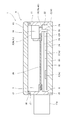
- such an electronic unit 1 is A casing 4 having an electronic component housing space 3 capable of housing the electronic component 2 therein; And a heat dissipating member 5 to which a heat-generating electronic component 2a that generates heat upon energization is attached. And the said casing 4 shall have the opening part 6 which can contact-fix the said heat radiating member 5. As shown in FIG. 1, such an electronic unit 1 is A casing 4 having an electronic component housing space 3 capable of housing the electronic component 2 therein; And a heat dissipating member 5 to which a heat-generating electronic component 2a that generates heat upon energization is attached. And the said casing 4 shall have the opening part 6 which can contact-fix the said heat radiating member 5. As shown in FIG.
- the electronic unit 1 is a PWM module for performing PWM control such as a radiator fan controller, for example.
- the electronic unit 1 is not limited to the above.
- the casing 4 includes a frame-shaped casing body 11, a lid body 13 that closes the opening 12 on the front surface side of the casing body 11, and a bottom surface member 14 that closes the opening 6 on the back surface side of the casing body 11. It is said.
- the casing body 11 is provided with a connection port portion 11a for connecting an external connector.
- the lid body 13 and the bottom member 14 are bonded and fixed with an adhesive to the peripheral edge portions of the openings 6 and 12 of the casing body 11 and sealed.
- an adhesive margin 15 for the peripheral edge of the bottom member 14 is formed at the peripheral edge of the opening 6 on the back side of the casing 4.
- an adhesive groove 17 for fitting and fixing the adhesive protrusion 16 formed on the peripheral edge of the lid 13 to the peripheral edge of the opening 12 on the surface side of the casing 4 by adhesive bonding is provided. It is formed.
- the exothermic electronic component 2a can be, for example, an exothermic semiconductor such as a MOS FET, a coil, or a shunt resistor.
- the heat-generating electronic component 2a is not limited to these.
- the heat generating electronic components 2a are collectively mounted on the circuit board 18.
- the heat radiating member 5 is a heat sink made of a metal having high heat conductivity such as aluminum.
- the circuit board 18 on which the heat generating electronic component 2a is mounted is fixed to the heat radiating member 5 via a heat transfer material 19 such as a heat transfer adhesive or a heat transfer sheet.
- the heat radiating member 5 is the bottom member 14 of the casing 4.
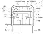
- this embodiment has the following configuration. (1) When the casing 4 fixes the heat radiating member 5 to the opening 6, the opening 6 is divided into a heat generating electronic component installation section 21 in which the heat generating electronic component 2 a is installed, and the heat generation.
- the partition wall 23 is divided into an adjacent section 22 adjacent to the section 21 for installing the sexual electronic component.
- the heat-generating electronic component installation section 21 is filled with a thermosetting potting material 24 for moisture prevention to a height at which at least the heat-generating electronic component 2a is buried.
- the adjacent section 22 communicates with a position inside the electronic component housing space 3 of the casing 4 away from the exothermic electronic component installation section 21 filled with the potting material 24. It is supposed to have.
- the heat generating electronic component installation section 21 is a closed region that occupies most of the opening 6 on the back surface side of the casing body 11.
- the circuit board 18 described above is attached mainly to a portion of the heat dissipating member 5 on the side of the heat generating electronic component installation section 21.
- the circuit board 18 can extend a portion where the heat-generating electronic component 2a is not mounted to the adjacent section 22 side, or can provide an extension.
- the adjacent section 22 is a relatively slightly closed area remaining in the opening 6 on the back surface side of the casing body 11.
- the adjacent section 22 is elongated along one side of the casing body 11 having a substantially rectangular shape in plan view. To divide is to divide the opening 6 with a boundary.
- the partition wall 23 has an edge on the opening 6 side as an abutting portion 26 that abuts against the surface of the heat radiating member 5, an extended portion of the circuit board 18, etc. It is considered as a bonding allowance for bonding.
- the partition wall 23 is formed as a dam plate for preventing the potting material 24 from entering the adjacent partition 22, and at least higher than the height at which the potting material 24 is filled.
- the potting material 24 is made of a resin having high thermal conductivity such as silicone.
- the potting material 24 is a section for installing an exothermic electronic component immediately after the adhesive is applied to the opening 6 on the back surface side of the casing 4 and the bottom member 14 is pasted before the adhesive is dried. After that, the resin is charged into a heat treatment furnace 21 and then immediately cured in a heating furnace, for example, at 80 degrees for 20 minutes.
- the communication portion 25 can be structurally configured such that the entire top surface of the adjacent section 22 is opened.
- the communication unit 25 will be described later.
- an electronic component installation wall portion 31 on which an electronic component 2 b different from the exothermic electronic component 2 a can be installed is formed.
- the communication part 25 is a communication hole 25 a formed in the electronic component installation wall part 31.
- the other electronic component 2b may be any electronic component 2 other than the heat-generating electronic component 2a in this case.
- the electronic component installation wall portion 31 is a horizontal wall that covers at least the top of the adjacent section 22.
- the electronic component installation wall 31 is a surface substantially parallel to the lid 13 and the bottom member 14.
- the electronic component installation wall 31 can also be provided with an uneven shape or the like according to another electronic component 2b to be installed.
- the electronic component installation wall 31 may have the same size as the top of the adjacent section 22 described above, or may have a size that protrudes from the top of the adjacent section 22 in accordance with another electronic component 2b to be installed. In this case, the latter is assumed.
- a wiring portion 35 is embedded in the electronic component installation wall portion 31 as necessary.
- the circuit board 18 and the electronic component 2 described above are electrically connected to the wiring portion 35.
- the electronic component 2 includes a wide range of exothermic electronic components 2a and other electronic components 2b.
- a through gap 36 or a filling port for filling the potting material 24 is appropriately formed above the exothermic electronic component installation section 21 in the electronic component installation wall 31.
- the through gap 36 is formed in the adjacent section 22, the wiring section 35, and the like.
- the communication holes 25a are small holes, and can be provided in an arbitrary number and in an arbitrary shape and size at an arbitrary position of the electronic component installation wall portion 31. However, in order to efficiently escape the air in the adjacent section 22 expanded by the heat during the heat treatment of the potting material 24, a plurality of communication holes 25a are arranged in a state as uniform as possible with respect to the electronic component installation wall portion 31. It is preferable to do this. On the other hand, in order to increase the heat insulating effect of the adjacent section 22, it is preferable that the communication holes 25a be as small and as small as possible. Therefore, the communication hole 25a is set in consideration of the balance between the air escape performance during the heat treatment for the potting material 24 and the heat insulation performance during normal operation.
- the electronic component installation wall 31 is provided with a locking claw 41 for locking and holding the other electronic component 2b.
- the communication hole 25a has a mold punching hole 42 formed when the locking claw 41 is molded.
- the locking claw 41 is integrally extended from the electronic component installation wall portion 31 toward another electronic component 2b.
- the mold punching hole 42 is a gap that can be formed at the base of the locking claw 41 after the sllite mold used for forming the locking claw 41 is retracted.
- the communication hole 25a may include a dedicated breathing hole in addition to the mold punching hole 42 for the locking claw 41.
- the other electronic component 2b is an electronic component 2c that is easily affected by heat.
- the electronic component 2c that is easily affected by heat that is, the heat-sensitive electronic component can be, for example, an electrolytic capacitor, a varistor, an oscillator, or the like.
- the electronic component 2c that is easily affected by heat is not limited thereto.
- the casing 4 houses and protects the electronic component 2 in the internal electronic component housing space 3.
- the opening part 6 was provided in this casing 4, and the heat radiating member 5 with which the heat-emitting electronic component 2a was attached to the opening part 6 was contact-fixed. Thereby, the heat generated by the heat-generating electronic component 2 a can be radiated from the entire surface of the heat radiating member 5 to the outside using the heat radiating member 5.
- the electronic unit 1 described above is manufactured as follows. That is, first, an electronic component 2, such as another electronic component 2b or an electronic component 2c that is easily affected by heat, is attached to the electronic component housing space 3 inside the casing 4. These electronic components 2 are fixed to the locking claws 41 and the like, and are electrically connected to the wiring portion 35. Next, an adhesive is applied to the opening 6 on the back surface side of the casing 4 to attach the bottom member 14. In this case, the bottom surface member 14 is particularly the heat radiating member 5 to which the circuit board 18 having the heat-generating electronic component 2a is attached in advance. Then, before the adhesive is dried, the potting material 24 is filled into the heat generating electronic component installing section 21 and immediately heated together with the casing 4 in a heating furnace to cure the potting material 24. Finally, an adhesive is applied to the opening 12 on the surface side of the casing 4 and the lid 13 is attached.
- an adhesive is applied to the opening 12 on the surface side of the casing 4 and the lid 13 is attached.
- a partition wall 23 is provided in the opening 6 of the casing 4. As a result, the opening 6 is divided into two regions of the exothermic electronic component installation section 21 and the adjacent section 22 by the partition wall 23 so that the adjacent section 22 where the exothermic electronic component 2a is not installed can be secured. As a result, it is possible to use the adjacent section 22 where the heat generating electronic component 2a is not installed as a heat insulating space.
- the heat-generating electronic component installation section 21 was filled with a thermosetting potting material 24 for moisture prevention to a height at which at least the heat-generating electronic component 2a was buried.
- the heat-generating electronic component 2a can be sealed with the thermosetting potting material 24 to have a moisture-proof function.
- the potting material 24 has a higher thermal conductivity than air, the heat generated by the heat-generating electronic component 2a by energization can be efficiently transmitted to the heat radiating member 5 and the like via the potting material 24. .
- the adjacent section 22 is not filled with the potting material 24. It is possible to minimize the amount of potting material 24 to be used, and it is possible to suppress an increase in cost and weight due to the potting material 24.
- the communication part 25 was provided in the adjacent division 22, and the adjacent division 22 and the position away from the exothermic electronic component installation division 21 in the electronic component accommodation space 3 of the casing 4 were connected.
- the air in the adjacent section 22 expanded by the heat of the heat treatment for curing the potting material 24 and the pressure thereof are actively released to portions other than the heat generating electronic component installation section 21 in the casing 4. be able to.
- the air in the adjacent compartment 22 expanded by the heat of the heat treatment is separated from the adhesive portion between the compartment wall 23 and the heat radiating member 5 that has not yet completely dried, and the compartment for installing the heat-generating electronic component.
- the moisture-proof effect by the potting material 24 becomes incomplete, and condensed water accumulates in the crater CR, so that the heat generating electronic component 2a and the heat generating electronic component 2a are attached to the circuit.
- This may cause a failure such as a short circuit due to water immersion, or a circuit breakage due to a phenomenon in which a material is lost due to migration, that is, ionization.
- the air in the adjacent section 22 expanded by the heat of the heat treatment is used for the heat generating electronic component installation section 21 other than the section 21 for installing the potting material 24 in the casing 4 by the communication portion 25.
- An electronic component installation wall 31 was formed on the top of the adjacent section 22. As a result, it is possible to close the adjacent section 22 with the electronic component installation wall portion 31 to form a heat-insulating space with high hermeticity, and use the electronic component installation wall portion 31 to form the top of the adjacent section 22. An electronic component 2b different from the heat-generating electronic component 2a can be positively installed at the position.
- a communication hole 25 a was formed as a communication part 25 in the electronic component installation wall part 31.
- a locking claw 41 was formed on the electronic component installation wall 31. Thereby, another electronic component 2 b can be easily locked and held on the electronic component installation wall portion 31 using the locking claw 41.
- a mold extraction hole 42 is formed at the base of the locking claw 41.
- This mold extraction hole 42 is used as at least a part of the communication hole 25a. I did it.
- another electronic component 2b is an electronic component 2c that is easily affected by heat.
- the electronic component 2c that is easily affected by heat can be disposed in the casing 4 at a position that is thermally farthest from the heat-generating electronic component 2a.
- the electronic component 2 c that is easily affected by heat is isolated from the heat radiating member 5 by the adjacent section 22.
- the heat-generating electronic component 2a generates heat by energization, and the heat generated in the heat-generating electronic component 2a is transmitted to the heat radiating member 5, so that even if the heat radiating member 5 radiates heat to the outside, It becomes possible to effectively protect the sensitive electronic component 2c from heat. Therefore, it is possible to eliminate the need to change the specifications of the electronic component 2c that is easily affected by heat to an expensive heat-resistant electronic component, for example, a heat-resistant capacitor, and accordingly, it is possible to reduce the component cost.
Landscapes
- Engineering & Computer Science (AREA)
- Microelectronics & Electronic Packaging (AREA)
- Physics & Mathematics (AREA)
- Condensed Matter Physics & Semiconductors (AREA)
- General Physics & Mathematics (AREA)
- Computer Hardware Design (AREA)
- Power Engineering (AREA)
- Thermal Sciences (AREA)
- Chemical & Material Sciences (AREA)
- Dispersion Chemistry (AREA)
- Cooling Or The Like Of Electrical Apparatus (AREA)
- Casings For Electric Apparatus (AREA)
Priority Applications (3)
| Application Number | Priority Date | Filing Date | Title |
|---|---|---|---|
| CN201580066300.2A CN107432090B (zh) | 2014-12-09 | 2015-09-04 | 电子设备 |
| EP15867496.0A EP3232748A1 (en) | 2014-12-09 | 2015-09-04 | Electronic unit |
| US15/534,825 US9943010B2 (en) | 2014-12-09 | 2015-09-04 | Electronic unit |
Applications Claiming Priority (2)
| Application Number | Priority Date | Filing Date | Title |
|---|---|---|---|
| JP2014-248663 | 2014-12-09 | ||
| JP2014248663A JP6328044B2 (ja) | 2014-12-09 | 2014-12-09 | 電子ユニット |
Publications (1)
| Publication Number | Publication Date |
|---|---|
| WO2016092919A1 true WO2016092919A1 (ja) | 2016-06-16 |
Family
ID=56107115
Family Applications (1)
| Application Number | Title | Priority Date | Filing Date |
|---|---|---|---|
| PCT/JP2015/075196 WO2016092919A1 (ja) | 2014-12-09 | 2015-09-04 | 電子ユニット |
Country Status (5)
| Country | Link |
|---|---|
| US (1) | US9943010B2 (zh) |
| EP (1) | EP3232748A1 (zh) |
| JP (1) | JP6328044B2 (zh) |
| CN (1) | CN107432090B (zh) |
| WO (1) | WO2016092919A1 (zh) |
Cited By (2)
| Publication number | Priority date | Publication date | Assignee | Title |
|---|---|---|---|---|
| CN113301756A (zh) * | 2021-06-07 | 2021-08-24 | 国网黑龙江省电力有限公司供电服务中心 | 一种高寒地区电能表数据采集信号强化器 |
| US20220132698A1 (en) * | 2020-10-22 | 2022-04-28 | Continental Automotive Gmbh | Electronic housing element comprising a radiator, and associated adjustment method |
Families Citing this family (2)
| Publication number | Priority date | Publication date | Assignee | Title |
|---|---|---|---|---|
| USD929477S1 (en) * | 2020-01-07 | 2021-08-31 | Worthington Cylinders Corporation | Electronic module for a tank lid |
| USD924952S1 (en) * | 2020-01-07 | 2021-07-13 | Worthington Cylinders Corporation | Electronic module for a tank lid |
Citations (6)
| Publication number | Priority date | Publication date | Assignee | Title |
|---|---|---|---|---|
| JPH0527526U (ja) * | 1991-09-19 | 1993-04-09 | 三菱重工業株式会社 | コントロールボツクスのトランス固定構造 |
| JPH0550788U (ja) * | 1991-12-02 | 1993-07-02 | 株式会社東芝 | パネルの取付構造 |
| JPH05166954A (ja) * | 1991-12-16 | 1993-07-02 | Nippondenso Co Ltd | Ic応用製品の防水構造 |
| JP2004228159A (ja) * | 2003-01-20 | 2004-08-12 | Calsonic Kansei Corp | Pwmモジュール |
| JP2010147260A (ja) * | 2008-12-19 | 2010-07-01 | Stanley Electric Co Ltd | 回路モジュール及びその密封方法 |
| JP2013165139A (ja) * | 2012-02-10 | 2013-08-22 | Honda Motor Co Ltd | 電子部品ユニットの封止構造及び製造方法 |
Family Cites Families (4)
| Publication number | Priority date | Publication date | Assignee | Title |
|---|---|---|---|---|
| US6614108B1 (en) * | 2000-10-23 | 2003-09-02 | Delphi Technologies, Inc. | Electronic package and method therefor |
| JP4043930B2 (ja) * | 2002-12-05 | 2008-02-06 | カルソニックカンセイ株式会社 | Pwmモジュール |
| DE102009054517B4 (de) * | 2009-12-10 | 2011-12-29 | Robert Bosch Gmbh | Elektronisches Steuergerät |
| WO2012144070A1 (ja) * | 2011-04-22 | 2012-10-26 | 三菱電機株式会社 | 半導体装置 |
-
2014
- 2014-12-09 JP JP2014248663A patent/JP6328044B2/ja active Active
-
2015
- 2015-09-04 WO PCT/JP2015/075196 patent/WO2016092919A1/ja active Application Filing
- 2015-09-04 EP EP15867496.0A patent/EP3232748A1/en not_active Withdrawn
- 2015-09-04 CN CN201580066300.2A patent/CN107432090B/zh active Active
- 2015-09-04 US US15/534,825 patent/US9943010B2/en active Active
Patent Citations (6)
| Publication number | Priority date | Publication date | Assignee | Title |
|---|---|---|---|---|
| JPH0527526U (ja) * | 1991-09-19 | 1993-04-09 | 三菱重工業株式会社 | コントロールボツクスのトランス固定構造 |
| JPH0550788U (ja) * | 1991-12-02 | 1993-07-02 | 株式会社東芝 | パネルの取付構造 |
| JPH05166954A (ja) * | 1991-12-16 | 1993-07-02 | Nippondenso Co Ltd | Ic応用製品の防水構造 |
| JP2004228159A (ja) * | 2003-01-20 | 2004-08-12 | Calsonic Kansei Corp | Pwmモジュール |
| JP2010147260A (ja) * | 2008-12-19 | 2010-07-01 | Stanley Electric Co Ltd | 回路モジュール及びその密封方法 |
| JP2013165139A (ja) * | 2012-02-10 | 2013-08-22 | Honda Motor Co Ltd | 電子部品ユニットの封止構造及び製造方法 |
Cited By (4)
| Publication number | Priority date | Publication date | Assignee | Title |
|---|---|---|---|---|
| US20220132698A1 (en) * | 2020-10-22 | 2022-04-28 | Continental Automotive Gmbh | Electronic housing element comprising a radiator, and associated adjustment method |
| US11844196B2 (en) * | 2020-10-22 | 2023-12-12 | Continental Automotive Gmbh | Electronic housing element comprising a radiator, and associated adjustment method |
| CN113301756A (zh) * | 2021-06-07 | 2021-08-24 | 国网黑龙江省电力有限公司供电服务中心 | 一种高寒地区电能表数据采集信号强化器 |
| CN113301756B (zh) * | 2021-06-07 | 2022-11-01 | 国网黑龙江省电力有限公司供电服务中心 | 一种高寒地区电能表数据采集信号强化器 |
Also Published As
| Publication number | Publication date |
|---|---|
| JP6328044B2 (ja) | 2018-05-23 |
| JP2016111249A (ja) | 2016-06-20 |
| EP3232748A1 (en) | 2017-10-18 |
| CN107432090B (zh) | 2019-10-29 |
| CN107432090A (zh) | 2017-12-01 |
| US20170347491A1 (en) | 2017-11-30 |
| US9943010B2 (en) | 2018-04-10 |
Similar Documents
| Publication | Publication Date | Title |
|---|---|---|
| JP4387314B2 (ja) | 電気接続箱 | |
| WO2016092919A1 (ja) | 電子ユニット | |
| JP2013197405A (ja) | 電子制御装置 | |
| US10820406B2 (en) | Circuit structure and electrical junction box | |
| US10117347B2 (en) | Accommodation device for electronic parts | |
| JP2008282931A (ja) | 電気回路装置 | |
| JP2010057345A (ja) | 電子制御装置 | |
| CN108352691B (zh) | 电路结构体及电气接线盒 | |
| JP6227937B2 (ja) | 車両用電子制御装置 | |
| US10462936B2 (en) | Electronic control unit | |
| JP4783054B2 (ja) | スイッチングユニット | |
| JP2014236139A (ja) | 電子制御機器 | |
| JP2017108007A5 (ja) | 発熱電子部品の放熱装置、その製造方法、および車載充電器 | |
| JP6255176B2 (ja) | 電子機器の熱管理構造 | |
| JP2014161136A (ja) | 電力変換装置 | |
| KR101063172B1 (ko) | 전자제어장치 | |
| JP2004031417A (ja) | 電力回路部の防水方法 | |
| JP5147929B2 (ja) | スイッチングユニット | |
| JP2016063086A (ja) | 回路基板及び電子制御装置 | |
| JP2006310558A (ja) | スイッチングユニット | |
| JP2017011027A (ja) | 回路基板の放熱構造 | |
| KR101418682B1 (ko) | 열전도성 필러를 이용한 차량의 전자 제어 장치 및 그 제조 방법 | |
| JP5712315B2 (ja) | 電子ユニット | |
| CN115004870A (zh) | 整流器 | |
| CN115734525A (zh) | 具有滑入式印刷电路板的电子控制单元 |
Legal Events
| Date | Code | Title | Description |
|---|---|---|---|
| 121 | Ep: the epo has been informed by wipo that ep was designated in this application |
Ref document number: 15867496 Country of ref document: EP Kind code of ref document: A1 |
|
| NENP | Non-entry into the national phase |
Ref country code: DE |
|
| WWE | Wipo information: entry into national phase |
Ref document number: 15534825 Country of ref document: US |
|
| REEP | Request for entry into the european phase |
Ref document number: 2015867496 Country of ref document: EP |