WO2016092919A1 - 電子ユニット - Google Patents
電子ユニット Download PDFInfo
- Publication number
- WO2016092919A1 WO2016092919A1 PCT/JP2015/075196 JP2015075196W WO2016092919A1 WO 2016092919 A1 WO2016092919 A1 WO 2016092919A1 JP 2015075196 W JP2015075196 W JP 2015075196W WO 2016092919 A1 WO2016092919 A1 WO 2016092919A1
- Authority
- WO
- WIPO (PCT)
- Prior art keywords
- electronic component
- heat
- casing
- potting material
- component installation
- Prior art date
Links
Images


Classifications
-
- H—ELECTRICITY
- H01—ELECTRIC ELEMENTS
- H01L—SEMICONDUCTOR DEVICES NOT COVERED BY CLASS H10
- H01L23/00—Details of semiconductor or other solid state devices
- H01L23/02—Containers; Seals
- H01L23/04—Containers; Seals characterised by the shape of the container or parts, e.g. caps, walls
- H01L23/053—Containers; Seals characterised by the shape of the container or parts, e.g. caps, walls the container being a hollow construction and having an insulating or insulated base as a mounting for the semiconductor body
-
- H—ELECTRICITY
- H05—ELECTRIC TECHNIQUES NOT OTHERWISE PROVIDED FOR
- H05K—PRINTED CIRCUITS; CASINGS OR CONSTRUCTIONAL DETAILS OF ELECTRIC APPARATUS; MANUFACTURE OF ASSEMBLAGES OF ELECTRICAL COMPONENTS
- H05K7/00—Constructional details common to different types of electric apparatus
- H05K7/20—Modifications to facilitate cooling, ventilating, or heating
- H05K7/2039—Modifications to facilitate cooling, ventilating, or heating characterised by the heat transfer by conduction from the heat generating element to a dissipating body
- H05K7/20436—Inner thermal coupling elements in heat dissipating housings, e.g. protrusions or depressions integrally formed in the housing
- H05K7/20445—Inner thermal coupling elements in heat dissipating housings, e.g. protrusions or depressions integrally formed in the housing the coupling element being an additional piece, e.g. thermal standoff
-
- H—ELECTRICITY
- H01—ELECTRIC ELEMENTS
- H01L—SEMICONDUCTOR DEVICES NOT COVERED BY CLASS H10
- H01L23/00—Details of semiconductor or other solid state devices
- H01L23/02—Containers; Seals
-
- H—ELECTRICITY
- H01—ELECTRIC ELEMENTS
- H01L—SEMICONDUCTOR DEVICES NOT COVERED BY CLASS H10
- H01L23/00—Details of semiconductor or other solid state devices
- H01L23/02—Containers; Seals
- H01L23/04—Containers; Seals characterised by the shape of the container or parts, e.g. caps, walls
-
- H—ELECTRICITY
- H01—ELECTRIC ELEMENTS
- H01L—SEMICONDUCTOR DEVICES NOT COVERED BY CLASS H10
- H01L23/00—Details of semiconductor or other solid state devices
- H01L23/16—Fillings or auxiliary members in containers or encapsulations, e.g. centering rings
- H01L23/18—Fillings characterised by the material, its physical or chemical properties, or its arrangement within the complete device
- H01L23/24—Fillings characterised by the material, its physical or chemical properties, or its arrangement within the complete device solid or gel at the normal operating temperature of the device
-
- H—ELECTRICITY
- H01—ELECTRIC ELEMENTS
- H01L—SEMICONDUCTOR DEVICES NOT COVERED BY CLASS H10
- H01L23/00—Details of semiconductor or other solid state devices
- H01L23/28—Encapsulations, e.g. encapsulating layers, coatings, e.g. for protection
-
- H—ELECTRICITY
- H05—ELECTRIC TECHNIQUES NOT OTHERWISE PROVIDED FOR
- H05K—PRINTED CIRCUITS; CASINGS OR CONSTRUCTIONAL DETAILS OF ELECTRIC APPARATUS; MANUFACTURE OF ASSEMBLAGES OF ELECTRICAL COMPONENTS
- H05K1/00—Printed circuits
- H05K1/02—Details
- H05K1/0201—Thermal arrangements, e.g. for cooling, heating or preventing overheating
- H05K1/0203—Cooling of mounted components
-
- H—ELECTRICITY
- H05—ELECTRIC TECHNIQUES NOT OTHERWISE PROVIDED FOR
- H05K—PRINTED CIRCUITS; CASINGS OR CONSTRUCTIONAL DETAILS OF ELECTRIC APPARATUS; MANUFACTURE OF ASSEMBLAGES OF ELECTRICAL COMPONENTS
- H05K5/00—Casings, cabinets or drawers for electric apparatus
-
- H—ELECTRICITY
- H05—ELECTRIC TECHNIQUES NOT OTHERWISE PROVIDED FOR
- H05K—PRINTED CIRCUITS; CASINGS OR CONSTRUCTIONAL DETAILS OF ELECTRIC APPARATUS; MANUFACTURE OF ASSEMBLAGES OF ELECTRICAL COMPONENTS
- H05K7/00—Constructional details common to different types of electric apparatus
- H05K7/20—Modifications to facilitate cooling, ventilating, or heating
- H05K7/20845—Modifications to facilitate cooling, ventilating, or heating for automotive electronic casings
- H05K7/20854—Heat transfer by conduction from internal heat source to heat radiating structure
-
- H—ELECTRICITY
- H01—ELECTRIC ELEMENTS
- H01L—SEMICONDUCTOR DEVICES NOT COVERED BY CLASS H10
- H01L23/00—Details of semiconductor or other solid state devices
- H01L23/34—Arrangements for cooling, heating, ventilating or temperature compensation ; Temperature sensing arrangements
- H01L23/36—Selection of materials, or shaping, to facilitate cooling or heating, e.g. heatsinks
-
- H—ELECTRICITY
- H01—ELECTRIC ELEMENTS
- H01L—SEMICONDUCTOR DEVICES NOT COVERED BY CLASS H10
- H01L2924/00—Indexing scheme for arrangements or methods for connecting or disconnecting semiconductor or solid-state bodies as covered by H01L24/00
- H01L2924/0001—Technical content checked by a classifier
- H01L2924/0002—Not covered by any one of groups H01L24/00, H01L24/00 and H01L2224/00
-
- H—ELECTRICITY
- H01—ELECTRIC ELEMENTS
- H01L—SEMICONDUCTOR DEVICES NOT COVERED BY CLASS H10
- H01L2924/00—Indexing scheme for arrangements or methods for connecting or disconnecting semiconductor or solid-state bodies as covered by H01L24/00
- H01L2924/10—Details of semiconductor or other solid state devices to be connected
- H01L2924/11—Device type
- H01L2924/13—Discrete devices, e.g. 3 terminal devices
- H01L2924/1304—Transistor
- H01L2924/1306—Field-effect transistor [FET]
- H01L2924/13091—Metal-Oxide-Semiconductor Field-Effect Transistor [MOSFET]
-
- H—ELECTRICITY
- H01—ELECTRIC ELEMENTS
- H01L—SEMICONDUCTOR DEVICES NOT COVERED BY CLASS H10
- H01L2924/00—Indexing scheme for arrangements or methods for connecting or disconnecting semiconductor or solid-state bodies as covered by H01L24/00
- H01L2924/19—Details of hybrid assemblies other than the semiconductor or other solid state devices to be connected
- H01L2924/1901—Structure
- H01L2924/1904—Component type
- H01L2924/19041—Component type being a capacitor
-
- H—ELECTRICITY
- H01—ELECTRIC ELEMENTS
- H01L—SEMICONDUCTOR DEVICES NOT COVERED BY CLASS H10
- H01L2924/00—Indexing scheme for arrangements or methods for connecting or disconnecting semiconductor or solid-state bodies as covered by H01L24/00
- H01L2924/19—Details of hybrid assemblies other than the semiconductor or other solid state devices to be connected
- H01L2924/1901—Structure
- H01L2924/1904—Component type
- H01L2924/19042—Component type being an inductor
-
- H—ELECTRICITY
- H01—ELECTRIC ELEMENTS
- H01L—SEMICONDUCTOR DEVICES NOT COVERED BY CLASS H10
- H01L2924/00—Indexing scheme for arrangements or methods for connecting or disconnecting semiconductor or solid-state bodies as covered by H01L24/00
- H01L2924/19—Details of hybrid assemblies other than the semiconductor or other solid state devices to be connected
- H01L2924/1901—Structure
- H01L2924/1904—Component type
- H01L2924/19043—Component type being a resistor
-
- H—ELECTRICITY
- H01—ELECTRIC ELEMENTS
- H01L—SEMICONDUCTOR DEVICES NOT COVERED BY CLASS H10
- H01L2924/00—Indexing scheme for arrangements or methods for connecting or disconnecting semiconductor or solid-state bodies as covered by H01L24/00
- H01L2924/19—Details of hybrid assemblies other than the semiconductor or other solid state devices to be connected
- H01L2924/191—Disposition
- H01L2924/19101—Disposition of discrete passive components
- H01L2924/19105—Disposition of discrete passive components in a side-by-side arrangement on a common die mounting substrate
Definitions
- This case concerns the electronic unit.
- Some electronic units include both a heat-generating electronic component that generates heat when energized and an electronic component that is susceptible to heat (for example, see Patent Document 1).
- a heat-generating electronic component that generates heat when energized
- an electronic component that is susceptible to heat for example, see Patent Document 1.
- the main purpose of this case is to solve the above-mentioned problems.
- a casing that can house electronic components inside, A heat dissipating member to which heat-generating electronic components that generate heat when energized are attached, and
- the casing is an electronic unit having an opening capable of abutting and fixing the heat dissipation member, When the casing fixes the heat radiating member to the opening, the opening is adjacent to the exothermic electronic component installation section where the exothermic electronic component is installed and the exothermic electronic component installation section.
- thermosetting potting material for moisture prevention is filled at least to a height at which the heat generating electronic component is buried
- the adjacent section has a communication portion that communicates with a position in the casing away from the section for installing the heat generating electronic component filled with the potting material.
- the above configuration can prevent the air in the adjacent section expanded by the heat of the heat treatment for curing the thermosetting potting material from entering the potting material.
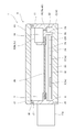
- such an electronic unit 1 is A casing 4 having an electronic component housing space 3 capable of housing the electronic component 2 therein; And a heat dissipating member 5 to which a heat-generating electronic component 2a that generates heat upon energization is attached. And the said casing 4 shall have the opening part 6 which can contact-fix the said heat radiating member 5. As shown in FIG. 1, such an electronic unit 1 is A casing 4 having an electronic component housing space 3 capable of housing the electronic component 2 therein; And a heat dissipating member 5 to which a heat-generating electronic component 2a that generates heat upon energization is attached. And the said casing 4 shall have the opening part 6 which can contact-fix the said heat radiating member 5. As shown in FIG.
- the electronic unit 1 is a PWM module for performing PWM control such as a radiator fan controller, for example.
- the electronic unit 1 is not limited to the above.
- the casing 4 includes a frame-shaped casing body 11, a lid body 13 that closes the opening 12 on the front surface side of the casing body 11, and a bottom surface member 14 that closes the opening 6 on the back surface side of the casing body 11. It is said.
- the casing body 11 is provided with a connection port portion 11a for connecting an external connector.
- the lid body 13 and the bottom member 14 are bonded and fixed with an adhesive to the peripheral edge portions of the openings 6 and 12 of the casing body 11 and sealed.
- an adhesive margin 15 for the peripheral edge of the bottom member 14 is formed at the peripheral edge of the opening 6 on the back side of the casing 4.
- an adhesive groove 17 for fitting and fixing the adhesive protrusion 16 formed on the peripheral edge of the lid 13 to the peripheral edge of the opening 12 on the surface side of the casing 4 by adhesive bonding is provided. It is formed.
- the exothermic electronic component 2a can be, for example, an exothermic semiconductor such as a MOS FET, a coil, or a shunt resistor.
- the heat-generating electronic component 2a is not limited to these.
- the heat generating electronic components 2a are collectively mounted on the circuit board 18.
- the heat radiating member 5 is a heat sink made of a metal having high heat conductivity such as aluminum.
- the circuit board 18 on which the heat generating electronic component 2a is mounted is fixed to the heat radiating member 5 via a heat transfer material 19 such as a heat transfer adhesive or a heat transfer sheet.
- the heat radiating member 5 is the bottom member 14 of the casing 4.
- this embodiment has the following configuration. (1) When the casing 4 fixes the heat radiating member 5 to the opening 6, the opening 6 is divided into a heat generating electronic component installation section 21 in which the heat generating electronic component 2 a is installed, and the heat generation.
- the partition wall 23 is divided into an adjacent section 22 adjacent to the section 21 for installing the sexual electronic component.
- the heat-generating electronic component installation section 21 is filled with a thermosetting potting material 24 for moisture prevention to a height at which at least the heat-generating electronic component 2a is buried.
- the adjacent section 22 communicates with a position inside the electronic component housing space 3 of the casing 4 away from the exothermic electronic component installation section 21 filled with the potting material 24. It is supposed to have.
- the heat generating electronic component installation section 21 is a closed region that occupies most of the opening 6 on the back surface side of the casing body 11.
- the circuit board 18 described above is attached mainly to a portion of the heat dissipating member 5 on the side of the heat generating electronic component installation section 21.
- the circuit board 18 can extend a portion where the heat-generating electronic component 2a is not mounted to the adjacent section 22 side, or can provide an extension.
- the adjacent section 22 is a relatively slightly closed area remaining in the opening 6 on the back surface side of the casing body 11.
- the adjacent section 22 is elongated along one side of the casing body 11 having a substantially rectangular shape in plan view. To divide is to divide the opening 6 with a boundary.
- the partition wall 23 has an edge on the opening 6 side as an abutting portion 26 that abuts against the surface of the heat radiating member 5, an extended portion of the circuit board 18, etc. It is considered as a bonding allowance for bonding.
- the partition wall 23 is formed as a dam plate for preventing the potting material 24 from entering the adjacent partition 22, and at least higher than the height at which the potting material 24 is filled.
- the potting material 24 is made of a resin having high thermal conductivity such as silicone.
- the potting material 24 is a section for installing an exothermic electronic component immediately after the adhesive is applied to the opening 6 on the back surface side of the casing 4 and the bottom member 14 is pasted before the adhesive is dried. After that, the resin is charged into a heat treatment furnace 21 and then immediately cured in a heating furnace, for example, at 80 degrees for 20 minutes.
- the communication portion 25 can be structurally configured such that the entire top surface of the adjacent section 22 is opened.
- the communication unit 25 will be described later.
- an electronic component installation wall portion 31 on which an electronic component 2 b different from the exothermic electronic component 2 a can be installed is formed.
- the communication part 25 is a communication hole 25 a formed in the electronic component installation wall part 31.
- the other electronic component 2b may be any electronic component 2 other than the heat-generating electronic component 2a in this case.
- the electronic component installation wall portion 31 is a horizontal wall that covers at least the top of the adjacent section 22.
- the electronic component installation wall 31 is a surface substantially parallel to the lid 13 and the bottom member 14.
- the electronic component installation wall 31 can also be provided with an uneven shape or the like according to another electronic component 2b to be installed.
- the electronic component installation wall 31 may have the same size as the top of the adjacent section 22 described above, or may have a size that protrudes from the top of the adjacent section 22 in accordance with another electronic component 2b to be installed. In this case, the latter is assumed.
- a wiring portion 35 is embedded in the electronic component installation wall portion 31 as necessary.
- the circuit board 18 and the electronic component 2 described above are electrically connected to the wiring portion 35.
- the electronic component 2 includes a wide range of exothermic electronic components 2a and other electronic components 2b.
- a through gap 36 or a filling port for filling the potting material 24 is appropriately formed above the exothermic electronic component installation section 21 in the electronic component installation wall 31.
- the through gap 36 is formed in the adjacent section 22, the wiring section 35, and the like.
- the communication holes 25a are small holes, and can be provided in an arbitrary number and in an arbitrary shape and size at an arbitrary position of the electronic component installation wall portion 31. However, in order to efficiently escape the air in the adjacent section 22 expanded by the heat during the heat treatment of the potting material 24, a plurality of communication holes 25a are arranged in a state as uniform as possible with respect to the electronic component installation wall portion 31. It is preferable to do this. On the other hand, in order to increase the heat insulating effect of the adjacent section 22, it is preferable that the communication holes 25a be as small and as small as possible. Therefore, the communication hole 25a is set in consideration of the balance between the air escape performance during the heat treatment for the potting material 24 and the heat insulation performance during normal operation.
- the electronic component installation wall 31 is provided with a locking claw 41 for locking and holding the other electronic component 2b.
- the communication hole 25a has a mold punching hole 42 formed when the locking claw 41 is molded.
- the locking claw 41 is integrally extended from the electronic component installation wall portion 31 toward another electronic component 2b.
- the mold punching hole 42 is a gap that can be formed at the base of the locking claw 41 after the sllite mold used for forming the locking claw 41 is retracted.
- the communication hole 25a may include a dedicated breathing hole in addition to the mold punching hole 42 for the locking claw 41.
- the other electronic component 2b is an electronic component 2c that is easily affected by heat.
- the electronic component 2c that is easily affected by heat that is, the heat-sensitive electronic component can be, for example, an electrolytic capacitor, a varistor, an oscillator, or the like.
- the electronic component 2c that is easily affected by heat is not limited thereto.
- the casing 4 houses and protects the electronic component 2 in the internal electronic component housing space 3.
- the opening part 6 was provided in this casing 4, and the heat radiating member 5 with which the heat-emitting electronic component 2a was attached to the opening part 6 was contact-fixed. Thereby, the heat generated by the heat-generating electronic component 2 a can be radiated from the entire surface of the heat radiating member 5 to the outside using the heat radiating member 5.
- the electronic unit 1 described above is manufactured as follows. That is, first, an electronic component 2, such as another electronic component 2b or an electronic component 2c that is easily affected by heat, is attached to the electronic component housing space 3 inside the casing 4. These electronic components 2 are fixed to the locking claws 41 and the like, and are electrically connected to the wiring portion 35. Next, an adhesive is applied to the opening 6 on the back surface side of the casing 4 to attach the bottom member 14. In this case, the bottom surface member 14 is particularly the heat radiating member 5 to which the circuit board 18 having the heat-generating electronic component 2a is attached in advance. Then, before the adhesive is dried, the potting material 24 is filled into the heat generating electronic component installing section 21 and immediately heated together with the casing 4 in a heating furnace to cure the potting material 24. Finally, an adhesive is applied to the opening 12 on the surface side of the casing 4 and the lid 13 is attached.
- an adhesive is applied to the opening 12 on the surface side of the casing 4 and the lid 13 is attached.
- a partition wall 23 is provided in the opening 6 of the casing 4. As a result, the opening 6 is divided into two regions of the exothermic electronic component installation section 21 and the adjacent section 22 by the partition wall 23 so that the adjacent section 22 where the exothermic electronic component 2a is not installed can be secured. As a result, it is possible to use the adjacent section 22 where the heat generating electronic component 2a is not installed as a heat insulating space.
- the heat-generating electronic component installation section 21 was filled with a thermosetting potting material 24 for moisture prevention to a height at which at least the heat-generating electronic component 2a was buried.
- the heat-generating electronic component 2a can be sealed with the thermosetting potting material 24 to have a moisture-proof function.
- the potting material 24 has a higher thermal conductivity than air, the heat generated by the heat-generating electronic component 2a by energization can be efficiently transmitted to the heat radiating member 5 and the like via the potting material 24. .
- the adjacent section 22 is not filled with the potting material 24. It is possible to minimize the amount of potting material 24 to be used, and it is possible to suppress an increase in cost and weight due to the potting material 24.
- the communication part 25 was provided in the adjacent division 22, and the adjacent division 22 and the position away from the exothermic electronic component installation division 21 in the electronic component accommodation space 3 of the casing 4 were connected.
- the air in the adjacent section 22 expanded by the heat of the heat treatment for curing the potting material 24 and the pressure thereof are actively released to portions other than the heat generating electronic component installation section 21 in the casing 4. be able to.
- the air in the adjacent compartment 22 expanded by the heat of the heat treatment is separated from the adhesive portion between the compartment wall 23 and the heat radiating member 5 that has not yet completely dried, and the compartment for installing the heat-generating electronic component.
- the moisture-proof effect by the potting material 24 becomes incomplete, and condensed water accumulates in the crater CR, so that the heat generating electronic component 2a and the heat generating electronic component 2a are attached to the circuit.
- This may cause a failure such as a short circuit due to water immersion, or a circuit breakage due to a phenomenon in which a material is lost due to migration, that is, ionization.
- the air in the adjacent section 22 expanded by the heat of the heat treatment is used for the heat generating electronic component installation section 21 other than the section 21 for installing the potting material 24 in the casing 4 by the communication portion 25.
- An electronic component installation wall 31 was formed on the top of the adjacent section 22. As a result, it is possible to close the adjacent section 22 with the electronic component installation wall portion 31 to form a heat-insulating space with high hermeticity, and use the electronic component installation wall portion 31 to form the top of the adjacent section 22. An electronic component 2b different from the heat-generating electronic component 2a can be positively installed at the position.
- a communication hole 25 a was formed as a communication part 25 in the electronic component installation wall part 31.
- a locking claw 41 was formed on the electronic component installation wall 31. Thereby, another electronic component 2 b can be easily locked and held on the electronic component installation wall portion 31 using the locking claw 41.
- a mold extraction hole 42 is formed at the base of the locking claw 41.
- This mold extraction hole 42 is used as at least a part of the communication hole 25a. I did it.
- another electronic component 2b is an electronic component 2c that is easily affected by heat.
- the electronic component 2c that is easily affected by heat can be disposed in the casing 4 at a position that is thermally farthest from the heat-generating electronic component 2a.
- the electronic component 2 c that is easily affected by heat is isolated from the heat radiating member 5 by the adjacent section 22.
- the heat-generating electronic component 2a generates heat by energization, and the heat generated in the heat-generating electronic component 2a is transmitted to the heat radiating member 5, so that even if the heat radiating member 5 radiates heat to the outside, It becomes possible to effectively protect the sensitive electronic component 2c from heat. Therefore, it is possible to eliminate the need to change the specifications of the electronic component 2c that is easily affected by heat to an expensive heat-resistant electronic component, for example, a heat-resistant capacitor, and accordingly, it is possible to reduce the component cost.
Abstract
熱硬化性のポッティング材を硬化するための加熱処理の熱によって膨張された断熱空間内部の空気が、ポッティング材の内部へ入り込まないようにする。 ケーシング(4)が、開口部(6)に放熱部材(5)を固定した時に、開口部(6)を、発熱性電子部品(2a)が設置される発熱性電子部品設置用区画(21)と、この発熱性電子部品設置用区画(21)に隣接する隣接区画(22)とに区切る区画壁(23)を有している。 発熱性電子部品設置用区画(21)内に、防湿のための熱硬化性のポッティング材(24)が、少なくとも発熱性電子部品(2a)が埋まる高さまで充填されている。 隣接区画(22)が、ケーシング(4)内の、ポッティング材(24)が充填された発熱性電子部品設置用区画(21)から離れた位置に連通する連通部(25)を有している。
Description
本件は、電子ユニットに関するものである。
自動車などの車両には、車体の各部に多数の電装品が設置されている。そして、これらの電装品を操作したり制御したりするのに多数の電子ユニットが用いられている。
このような電子ユニットには、通電によって発熱する発熱性電子部品と、熱に影響を受け易い電子部品とを両方同時に備えたものが存在している(例えば、特許文献1参照)。そして、このような構成を有する電子ユニットでは、発熱性電子部品が発生する熱から、熱に影響を受け易い電子部品を保護する必要がある。
そこで、特許文献1に記載された電子ユニットでは、1つのケーシング内に、発熱性電子部品と、熱に影響を受け易い電子部品とを、間に断熱用密閉空間を介在させるなどして、分離配置するようにしていた。更に、発熱性電子部品と、熱に影響を受け易い電子部品との両者を、防湿のために、空気よりも熱伝導率の高い、熱硬化性のポッティング材でそれぞれ別個に封止するようにしていた。
上記電子ユニットでは、ポッティング材を硬化させるために加熱処理が行われるが、この時の熱によって断熱用密閉空間内部の空気が膨張する。そして、膨張した断熱用密閉空間内部の空気がポッティング材の内部へ入り込むと、ポッティング材に気泡を生じさせたり、この気泡が成長し限界に達して破裂することでクレーターを生じさせたりするようなことが起きる。
このように、ポッティング材にクレーターが生じると、ポッティング材による防湿効果が不完全となるため、クレーターに結露水が溜まるなどして電子部品、特に、発熱性電子部品や熱に影響を受け易い電子部品や、電子部品が取付けられた回路に、浸水によるショートを発生させたり、または、マイグレーション、即ち、イオン化によって材質が欠損する現象による回路の破損が起きたりする、などの不具合が生じるおそれがある。
そこで、本件は、上記した問題点を解決することを、主な目的としている。
上記課題を解決するために、本件は、
内部に電子部品を収容可能なケーシングと、
通電によって発熱する発熱性電子部品が取付けられた放熱部材と、を備えていると共に、
前記ケーシングが、前記放熱部材を当接固定可能な開口部を有する電子ユニットであって、
前記ケーシングが、前記開口部に前記放熱部材を固定した時に、前記開口部を、前記発熱性電子部品が設置される発熱性電子部品設置用区画と、該発熱性電子部品設置用区画に隣接する隣接区画とに区切る区画壁を有しており、
前記発熱性電子部品設置用区画内に、防湿のための熱硬化性のポッティング材が、少なくとも前記発熱性電子部品が埋まる高さまで充填されており、
前記隣接区画が、前記ケーシング内の、前記ポッティング材が充填された前記発熱性電子部品設置用区画から離れた位置に連通する連通部を有していることを特徴とする。
本件によれば、上記構成によって、熱硬化性のポッティング材を硬化させるための加熱処理の熱によって膨張された隣接区画内の空気が、ポッティング材の内部へ入り込まないようにすることができる。
以下、本実施の形態を、図面を用いて詳細に説明する。
図1~図4は、この実施の形態を説明するためのものである。
図1~図4は、この実施の形態を説明するためのものである。
<構成>以下、この実施例の構成について説明する。
自動車などの車両には、車体の各部に多数の電装品が設置されている。そして、これらの電装品を操作したり制御したりするのに多数の電子ユニットが用いられている。
自動車などの車両には、車体の各部に多数の電装品が設置されている。そして、これらの電装品を操作したり制御したりするのに多数の電子ユニットが用いられている。
図1に示すように、このような電子ユニット1は、
内部に電子部品2を収容可能な電子部品収容空間3を有するケーシング4と、
通電によって発熱する発熱性電子部品2aが取付けられた放熱部材5と、を備えたものとされている。
そして、上記ケーシング4が、上記放熱部材5を当接固定可能な開口部6を有するものとされている。
内部に電子部品2を収容可能な電子部品収容空間3を有するケーシング4と、
通電によって発熱する発熱性電子部品2aが取付けられた放熱部材5と、を備えたものとされている。
そして、上記ケーシング4が、上記放熱部材5を当接固定可能な開口部6を有するものとされている。
ここで、電子ユニット1は、例えば、ラジエータファンのコントローラなどのようなPWM制御を行うためのPWMモジュールとされる。但し、電子ユニット1は、上記に限るものではない。
ケーシング4は、枠状のケーシング本体11と、このケーシング本体11の表面側の開口部12を塞ぐ蓋体13と、ケーシング本体11の裏面側の開口部6を塞ぐ底面部材14と、を有するものとされる。ケーシング本体11には、外部のコネクタを接続するための接続口部11aなどが設けられる。蓋体13および底面部材14は、それぞれケーシング本体11の開口部6,12の周縁部に対して接着剤で接着固定されてシールされる。そのために、ケーシング4の裏面側の開口部6の周縁部には、底面部材14の周縁部に対する接着代15が形成される。また、ケーシング4の表面側の開口部12の周縁部には、蓋体13の周縁部に形成された接着用凸条16を、嵌合して接着剤接着固定するための接着用溝部17が形成される。
発熱性電子部品2aは、例えば、MOS型FETなどの発熱性半導体や、コイルや、シャント抵抗などとすることができる。但し、発熱性電子部品2aは、これらに限るものではない。発熱性電子部品2aは、回路基板18にまとめて実装される。
放熱部材5は、アルミなどの伝熱性の高い金属によってできたヒートシンクなどとされる。放熱部材5に対し、発熱性電子部品2aが実装された回路基板18は、伝熱性接着剤や伝熱シートなどの伝熱材19を介して固定される。この場合、放熱部材5は、ケーシング4の底面部材14とされる。このように底面部材14を放熱部材5とすることにより、発熱性電子部品2aが発生する熱を、広い面積で効率的に外部へ逃がす、即ち、放熱することが可能となる。
以上のような基本的な構成に対し、この実施例では、以下のような構成を備えるようにしている。
(1)上記ケーシング4が、上記開口部6に上記放熱部材5を固定した時に、上記開口部6を、上記発熱性電子部品2aが設置される発熱性電子部品設置用区画21と、この発熱性電子部品設置用区画21に隣接する隣接区画22と、に区切る区画壁23を有している。
そして、上記発熱性電子部品設置用区画21内に、防湿のための熱硬化性のポッティング材24が、少なくとも上記発熱性電子部品2aが埋まる高さまで充填されている。
これに対し、上記隣接区画22が、上記ケーシング4の電子部品収容空間3内部の、上記ポッティング材24が充填された上記発熱性電子部品設置用区画21から離れた位置に連通する連通部25を有するものとされている。
この場合、発熱性電子部品設置用区画21は、ケーシング本体11の裏面側の開口部6の大部分を占める閉じた領域とされる。上記した回路基板18は、主に、放熱部材5における、発熱性電子部品設置用区画21側の部分に取付けられる。但し、構造的には、回路基板18は、発熱性電子部品2aが実装されていない部分を、隣接区画22の側へ延ばす、または、延長部を設けることもできる。
隣接区画22は、ケーシング本体11の裏面側の開口部6の残りの比較的僅かな閉じた領域とされる。この場合、隣接区画22は、平面視ほぼ矩形状をしたケーシング本体11の一辺に沿った細長いものとされる。区切るとは、開口部6に境目を付けて分けることである。
区画壁23は、開口部6側の縁部が放熱部材5の面や回路基板18の延長部などに当接する当接部26とされると共に、放熱部材5や回路基板18の延長部などに接着するための接着代とされる。区画壁23は、ポッティング材24が隣接区画22へ入るのを防止するための堰板として、少なくとも、ポッティング材24を充填する高さよりも高く形成される。
ポッティング材24には、シリコーン系などの熱伝導性の高い樹脂が使用される。生産性向上のため、ポッティング材24は、ケーシング4の裏面側の開口部6に接着剤を塗布して底面部材14を貼り付けた直後、接着剤が乾かないうちに発熱性電子部品設置用区画21へ充填され、その後、直ちに加熱炉で、例えば、80度で20分などに加熱処理されて硬化されるようにしている。
連通部25は、構造的には、隣接区画22の頂部全面を開放したものなどとすることも可能である。連通部25については、後述する。
(2)上記隣接区画22の頂部に、上記発熱性電子部品2aとは別の電子部品2bを設置可能な電子部品設置壁部31が形成されている。
上記連通部25が、上記電子部品設置壁部31に形成された連通孔25aとされている。
上記連通部25が、上記電子部品設置壁部31に形成された連通孔25aとされている。
ここで、別の電子部品2bは、この場合、発熱性電子部品2a以外の電子部品2であれば、何でも良い。
電子部品設置壁部31は、少なくとも隣接区画22の頂部を覆う横壁とされる。電子部品設置壁部31は、蓋体13および底面部材14とほぼ平行な面とされる。但し、電子部品設置壁部31には、設置される別の電子部品2bに応じた凹凸形状などを設けることもできる。電子部品設置壁部31は、上記した隣接区画22の頂部と同じ大きさにしても良いし、設置される別の電子部品2bに合わせて隣接区画22の頂部からハミ出す大きさとしても良い。この場合には、後者としている。電子部品設置壁部31の内部などには、必要に応じて配線部35が埋設される。上記した回路基板18や、電子部品2は、この配線部35に対して電気的に接続される。この場合、電子部品2には、発熱性電子部品2aや別の電子部品2bなどが広く含まれるものとする。なお、電子部品設置壁部31における発熱性電子部品設置用区画21の上側には、ポッティング材24を充填するなどのための貫通隙間部36または充填口が適宜形成される。この貫通隙間部36は、隣接区画22や配線部35などに形成される。
連通孔25aは、小孔のことであり、電子部品設置壁部31の任意の位置に、任意の形状および大きさで、任意の数だけ設けることができる。但し、ポッティング材24の加熱処理時の熱で膨張された隣接区画22内部の空気を効率良く逃がすためには、連通孔25aは、電子部品設置壁部31に対してできるだけ均等な状態で複数配置するのが好ましい。これに対し、隣接区画22の断熱効果を上げるためには、連通孔25aは、できるだけ小さく、且つ、少なくするのが好ましい。よって、連通孔25aは、上記したポッティング材24に対する加熱処理時の空気の逃げ性と、通常時の断熱性とのバランスを考慮して設定する。
(3)上記電子部品設置壁部31に、上記別の電子部品2bを係止保持するための係止爪41が設けられている。
上記連通孔25aが、上記係止爪41を成形する際に形成される型抜孔42を有している。
上記連通孔25aが、上記係止爪41を成形する際に形成される型抜孔42を有している。
ここで、係止爪41は、例えば、電子部品設置壁部31から、別の電子部品2bの側へ向けて一体に延びるものとされる。型抜孔42は、係止爪41を成形するために用いたスライト型を退避させた後に係止爪41の基部にできる空隙部である。なお、連通孔25aは、係止爪41のための型抜孔42以外に、専用の呼吸孔などを含むものとしても良い。
(4)上記別の電子部品2bが、熱に影響を受け易い電子部品2cとされている。
ここで、熱に影響を受け易い電子部品2c、即ち、熱影響性電子部品は、例えば、電解コンデンサや、バリスタや、発振子などとすることができる。但し、熱に影響を受け易い電子部品2cは、これらに限るものではない。
<作用>以下、この実施例の作用について説明する。
ケーシング4は、電子部品2を、内部の電子部品収容空間3に収容して保護するものである。そして、このケーシング4に開口部6を設けて、開口部6に発熱性電子部品2aが取付けられた放熱部材5を当接固定するようにした。これにより、発熱性電子部品2aが発生した熱を、放熱部材5を用いて、放熱部材5の全面から外部へ放熱することができる。
ケーシング4は、電子部品2を、内部の電子部品収容空間3に収容して保護するものである。そして、このケーシング4に開口部6を設けて、開口部6に発熱性電子部品2aが取付けられた放熱部材5を当接固定するようにした。これにより、発熱性電子部品2aが発生した熱を、放熱部材5を用いて、放熱部材5の全面から外部へ放熱することができる。
上記した電子ユニット1は、以下のようにして製造される。即ち、先ず、ケーシング4内部の電子部品収容空間3に電子部品2、例えば、別の電子部品2bや熱に影響を受け易い電子部品2cなどを取付ける。これらの電子部品2は、係止爪41などに固定されると共に、配線部35に対して電気的に接続される。次に、ケーシング4の裏面側の開口部6に接着剤を塗布して底面部材14を貼り付ける。この場合、底面部材14は、特に、発熱性電子部品2aを有する回路基板18が予め取付けられた放熱部材5とされる。そして、この接着剤が乾かないうちにポッティング材24を、発熱性電子部品設置用区画21へ充填し、直ちに加熱炉でケーシング4ごと加熱処理してポッティング材24を硬化させる。最後に、ケーシング4の表面側の開口部12に接着剤を塗布して蓋体13を貼り付ける。
<効果>この実施例によれば、以下のような効果を得ることができる。
(1)ケーシング4の開口部6に区画壁23を設けた。これにより、開口部6を区画壁23で発熱性電子部品設置用区画21と隣接区画22との2つの領域に区切って、発熱性電子部品2aが設置されない隣接区画22を確保できるようにした。その結果、発熱性電子部品2aが設置されない隣接区画22を断熱空間として利用することが可能となる。
(1)ケーシング4の開口部6に区画壁23を設けた。これにより、開口部6を区画壁23で発熱性電子部品設置用区画21と隣接区画22との2つの領域に区切って、発熱性電子部品2aが設置されない隣接区画22を確保できるようにした。その結果、発熱性電子部品2aが設置されない隣接区画22を断熱空間として利用することが可能となる。
そして、発熱性電子部品設置用区画21に対し、防湿のための熱硬化性のポッティング材24を、少なくとも発熱性電子部品2aが埋まる高さまで充填した。これにより、発熱性電子部品2aを熱硬化性のポッティング材24で封止して防湿機能を持たせることができる。また、ポッティング材24は、空気よりも熱伝導率が高いので、通電によって発熱性電子部品2aが発生した熱を、ポッティング材24を介して効率的に放熱部材5などへ伝えることが可能となる。加えて、発熱性電子部品設置用区画21に充填されるポッティング材24を発熱性電子部品2aが埋まる程度の高さに抑えると共に、隣接区画22にポッティング材24が充填されないようにすることで、使用するポッティング材24の量を最小限に抑えることが可能となり、ポッティング材24によるコスト増加と重量増加とを抑えることができる。
更に、隣接区画22に連通部25を設けて、隣接区画22と、ケーシング4の電子部品収容空間3内部における、発熱性電子部品設置用区画21から離れた位置とを連通させるようにした。これにより、ポッティング材24を硬化させるための加熱処理の熱で膨張された隣接区画22内部の空気やその圧力を、ケーシング4内の発熱性電子部品設置用区画21以外の部分に積極的に逃すことができる。その結果、加熱処理の熱で膨張された隣接区画22内部の空気が、区画壁23と放熱部材5との間の、まだ完全に乾いていないような接着部分から、発熱性電子部品設置用区画21へ侵入してポッティング材24の内部に入り込み、ポッティング材24に気泡を生じさせたり、この気泡が成長して限界に達し破裂することで、図2に仮想線で示すようなクレーターCRを生じさせたりするような不具合を防止できる。
なお、ポッティング材24にクレーターCRが生じると、ポッティング材24による防湿効果が不完全となり、クレーターCRに結露水が溜まるなどして発熱性電子部品2aや発熱性電子部品2aが取付けられた回路に、浸水によるショートを発生させたり、マイグレーション、即ち、イオン化によって材質が欠損する現象による回路破損を起こしたりするなどの故障を生じることになる。
これに対し、上記したように、加熱処理の熱で膨張された隣接区画22内部の空気を、連通部25によって、ケーシング4内のポッティング材24が充填された発熱性電子部品設置用区画21以外の部分へ積極的に逃がすことで、発熱性電子部品設置用区画21へ充填されたポッティング材24を健全な状態に保つことができるようになり、上記したような不具合の発生を防止することが可能となる。
(2)隣接区画22の頂部に電子部品設置壁部31を形成した。これにより、隣接区画22を電子部品設置壁部31で閉止して、密閉性の高い断熱空間にすることが可能になると共に、電子部品設置壁部31を利用して、隣接区画22の頂部の位置に発熱性電子部品2aとは別の電子部品2bを積極的に設置することが可能となる。
また、電子部品設置壁部31に、連通部25として、連通孔25aを形成した。これにより、ポッティング材24を硬化させるための加熱処理の熱で膨張された隣接区画22内の空気やその圧力を、連通孔25aを介して、電子部品設置壁部31の反対側へ無理なく確実に逃すことができる。また、連通部25を連通孔25aとすることにより、隣接区画22に対する空気の出入りを極力抑えることができるので、隣接区画22による断熱性を高めることができる。
(3)電子部品設置壁部31に係止爪41を形成した。これにより、係止爪41を用いて電子部品設置壁部31に、別の電子部品2bを簡単に係止保持することができる。
しかも、型構造上、係止爪41を成形する際には係止爪41の基部に型抜孔42が作られることになるが、この型抜孔42を、連通孔25aの少なくとも一部として利用するようにした。これにより、係止爪41を設けることで、同時に連通孔25aも得ることができるので、効率的であり、構造的に無駄がない。
(4)特に、別の電子部品2bを、熱に影響を受け易い電子部品2cとした。これにより、熱に影響を受け易い電子部品2cを、ケーシング4内で、発熱性電子部品2aから熱的に最も遠い位置に配置することが可能となる。また、熱に影響を受け易い電子部品2cは、隣接区画22によって放熱部材5から隔離されることになる。その結果、通電によって発熱性電子部品2aが熱を発生し、発熱性電子部品2aで発生した熱が放熱部材5へ伝えられて、放熱部材5が全面で外部へ放熱を行っても、熱に影響を受け易い電子部品2cを、熱から有効に保護することが可能となる。よって、熱に影響を受け易い電子部品2cを、高価な耐熱性電子部品、例えば、耐熱コンデンサなどに仕様変更する必要をなくすことができ、その分、部品コストを抑えることが可能となる。
また、ケーシング4内部に、発熱性電子部品2aと熱に影響を受け易い電子部品2cとをスペース効率良く配置することが可能となり、ケーシング4をコンパクト化することができる。
以上、実施例を図面により詳述してきたが、実施例は例示にしか過ぎないものである。よって、実施例の構成にのみ限定されるものではなく、要旨を逸脱しない範囲の設計の変更等があっても本件に含まれることは勿論である。また、例えば、各実施例に複数の構成が含まれている場合には、特に記載がなくとも、これらの構成の可能な組合せが含まれることは勿論である。また、複数の実施例や変形例が本件のものとして開示されている場合には、特に記載がなくとも、これらに跨がった構成の組合せのうちの可能なものが含まれることは勿論である。また、図面に描かれている構成については、特に記載がなくとも、含まれることは勿論である。更に、「等」の用語がある場合には、同等のものを含むという意味で用いられている。また、「ほぼ」「約」「程度」などの用語がある場合には、常識的に認められる範囲や精度のものを含むという意味で用いられている。
1 電子ユニット
2 電子部品
2a 発熱性電子部品
2b 別の電子部品
2c 熱に影響を受け易い電子部品
3 電子部品収容空間
4 ケーシング
5 放熱部材
6 開口部
21 発熱性電子部品設置用区画
22 隣接区画
23 区画壁
24 ポッティング材
25 連通部
25a 連通孔
31 電子部品設置壁部
41 係止爪
42 型抜孔
2 電子部品
2a 発熱性電子部品
2b 別の電子部品
2c 熱に影響を受け易い電子部品
3 電子部品収容空間
4 ケーシング
5 放熱部材
6 開口部
21 発熱性電子部品設置用区画
22 隣接区画
23 区画壁
24 ポッティング材
25 連通部
25a 連通孔
31 電子部品設置壁部
41 係止爪
42 型抜孔
本出願は、2014年12月9日に、日本国特許庁に出願された特願2014-248663に基づいて優先権を主張し、その全ての開示は、完全に本明細書で参照により組み込まれる。
Claims (4)
- 内部に電子部品を収容可能なケーシングと、
通電によって発熱する発熱性電子部品が取付けられた放熱部材と、を備えていると共に、
前記ケーシングが、前記放熱部材を当接固定可能な開口部を有する電子ユニットであって、
前記ケーシングが、前記開口部に前記放熱部材を固定した時に、前記開口部を、前記発熱性電子部品が設置される発熱性電子部品設置用区画と、該発熱性電子部品設置用区画に隣接する隣接区画とに区切る区画壁を有しており、
前記発熱性電子部品設置用区画内に、防湿のための熱硬化性のポッティング材が、少なくとも前記発熱性電子部品が埋まる高さまで充填されており、
前記隣接区画が、前記ケーシング内の、前記ポッティング材が充填された前記発熱性電子部品設置用区画から離れた位置に連通する連通部を有していることを特徴とする電子ユニット。 - 請求項1に記載の電子ユニットであって、
前記隣接区画の頂部に、前記発熱性電子部品とは別の電子部品を設置可能な電子部品設置壁部が形成されており、
前記連通部が、前記電子部品設置壁部に形成された連通孔であることを特徴とする電子ユニット。 - 請求項2に記載の電子ユニットであって、
前記電子部品設置壁部に、前記別の電子部品を係止保持するための係止爪が設けられており、
前記連通孔が、前記係止爪を成形する際に形成される型抜孔を有していることを特徴とする電子ユニット。 - 請求項2に記載の電子ユニットであって、
前記別の電子部品が、熱に影響を受け易い電子部品であることを特徴とする電子ユニット。
Priority Applications (3)
| Application Number | Priority Date | Filing Date | Title |
|---|---|---|---|
| US15/534,825 US9943010B2 (en) | 2014-12-09 | 2015-09-04 | Electronic unit |
| CN201580066300.2A CN107432090B (zh) | 2014-12-09 | 2015-09-04 | 电子设备 |
| EP15867496.0A EP3232748A1 (en) | 2014-12-09 | 2015-09-04 | Electronic unit |
Applications Claiming Priority (2)
| Application Number | Priority Date | Filing Date | Title |
|---|---|---|---|
| JP2014248663A JP6328044B2 (ja) | 2014-12-09 | 2014-12-09 | 電子ユニット |
| JP2014-248663 | 2014-12-09 |
Publications (1)
| Publication Number | Publication Date |
|---|---|
| WO2016092919A1 true WO2016092919A1 (ja) | 2016-06-16 |
Family
ID=56107115
Family Applications (1)
| Application Number | Title | Priority Date | Filing Date |
|---|---|---|---|
| PCT/JP2015/075196 WO2016092919A1 (ja) | 2014-12-09 | 2015-09-04 | 電子ユニット |
Country Status (5)
| Country | Link |
|---|---|
| US (1) | US9943010B2 (ja) |
| EP (1) | EP3232748A1 (ja) |
| JP (1) | JP6328044B2 (ja) |
| CN (1) | CN107432090B (ja) |
| WO (1) | WO2016092919A1 (ja) |
Cited By (2)
| Publication number | Priority date | Publication date | Assignee | Title |
|---|---|---|---|---|
| CN113301756A (zh) * | 2021-06-07 | 2021-08-24 | 国网黑龙江省电力有限公司供电服务中心 | 一种高寒地区电能表数据采集信号强化器 |
| US20220132698A1 (en) * | 2020-10-22 | 2022-04-28 | Continental Automotive Gmbh | Electronic housing element comprising a radiator, and associated adjustment method |
Families Citing this family (2)
| Publication number | Priority date | Publication date | Assignee | Title |
|---|---|---|---|---|
| USD924952S1 (en) * | 2020-01-07 | 2021-07-13 | Worthington Cylinders Corporation | Electronic module for a tank lid |
| USD929477S1 (en) * | 2020-01-07 | 2021-08-31 | Worthington Cylinders Corporation | Electronic module for a tank lid |
Citations (6)
| Publication number | Priority date | Publication date | Assignee | Title |
|---|---|---|---|---|
| JPH0527526U (ja) * | 1991-09-19 | 1993-04-09 | 三菱重工業株式会社 | コントロールボツクスのトランス固定構造 |
| JPH05166954A (ja) * | 1991-12-16 | 1993-07-02 | Nippondenso Co Ltd | Ic応用製品の防水構造 |
| JPH0550788U (ja) * | 1991-12-02 | 1993-07-02 | 株式会社東芝 | パネルの取付構造 |
| JP2004228159A (ja) * | 2003-01-20 | 2004-08-12 | Calsonic Kansei Corp | Pwmモジュール |
| JP2010147260A (ja) * | 2008-12-19 | 2010-07-01 | Stanley Electric Co Ltd | 回路モジュール及びその密封方法 |
| JP2013165139A (ja) * | 2012-02-10 | 2013-08-22 | Honda Motor Co Ltd | 電子部品ユニットの封止構造及び製造方法 |
Family Cites Families (4)
| Publication number | Priority date | Publication date | Assignee | Title |
|---|---|---|---|---|
| US6614108B1 (en) * | 2000-10-23 | 2003-09-02 | Delphi Technologies, Inc. | Electronic package and method therefor |
| JP4043930B2 (ja) * | 2002-12-05 | 2008-02-06 | カルソニックカンセイ株式会社 | Pwmモジュール |
| DE102009054517B4 (de) * | 2009-12-10 | 2011-12-29 | Robert Bosch Gmbh | Elektronisches Steuergerät |
| JP5847165B2 (ja) * | 2011-04-22 | 2016-01-20 | 三菱電機株式会社 | 半導体装置 |
-
2014
- 2014-12-09 JP JP2014248663A patent/JP6328044B2/ja active Active
-
2015
- 2015-09-04 WO PCT/JP2015/075196 patent/WO2016092919A1/ja active Application Filing
- 2015-09-04 US US15/534,825 patent/US9943010B2/en active Active
- 2015-09-04 EP EP15867496.0A patent/EP3232748A1/en not_active Withdrawn
- 2015-09-04 CN CN201580066300.2A patent/CN107432090B/zh active Active
Patent Citations (6)
| Publication number | Priority date | Publication date | Assignee | Title |
|---|---|---|---|---|
| JPH0527526U (ja) * | 1991-09-19 | 1993-04-09 | 三菱重工業株式会社 | コントロールボツクスのトランス固定構造 |
| JPH0550788U (ja) * | 1991-12-02 | 1993-07-02 | 株式会社東芝 | パネルの取付構造 |
| JPH05166954A (ja) * | 1991-12-16 | 1993-07-02 | Nippondenso Co Ltd | Ic応用製品の防水構造 |
| JP2004228159A (ja) * | 2003-01-20 | 2004-08-12 | Calsonic Kansei Corp | Pwmモジュール |
| JP2010147260A (ja) * | 2008-12-19 | 2010-07-01 | Stanley Electric Co Ltd | 回路モジュール及びその密封方法 |
| JP2013165139A (ja) * | 2012-02-10 | 2013-08-22 | Honda Motor Co Ltd | 電子部品ユニットの封止構造及び製造方法 |
Cited By (4)
| Publication number | Priority date | Publication date | Assignee | Title |
|---|---|---|---|---|
| US20220132698A1 (en) * | 2020-10-22 | 2022-04-28 | Continental Automotive Gmbh | Electronic housing element comprising a radiator, and associated adjustment method |
| US11844196B2 (en) * | 2020-10-22 | 2023-12-12 | Continental Automotive Gmbh | Electronic housing element comprising a radiator, and associated adjustment method |
| CN113301756A (zh) * | 2021-06-07 | 2021-08-24 | 国网黑龙江省电力有限公司供电服务中心 | 一种高寒地区电能表数据采集信号强化器 |
| CN113301756B (zh) * | 2021-06-07 | 2022-11-01 | 国网黑龙江省电力有限公司供电服务中心 | 一种高寒地区电能表数据采集信号强化器 |
Also Published As
| Publication number | Publication date |
|---|---|
| EP3232748A1 (en) | 2017-10-18 |
| US20170347491A1 (en) | 2017-11-30 |
| US9943010B2 (en) | 2018-04-10 |
| CN107432090B (zh) | 2019-10-29 |
| CN107432090A (zh) | 2017-12-01 |
| JP2016111249A (ja) | 2016-06-20 |
| JP6328044B2 (ja) | 2018-05-23 |
Similar Documents
| Publication | Publication Date | Title |
|---|---|---|
| JP4387314B2 (ja) | 電気接続箱 | |
| WO2016092919A1 (ja) | 電子ユニット | |
| JP2013197405A (ja) | 電子制御装置 | |
| JP2008282931A (ja) | 電気回路装置 | |
| US20160212882A1 (en) | Control electronics | |
| JP2010057345A (ja) | 電子制御装置 | |
| US10820406B2 (en) | Circuit structure and electrical junction box | |
| CN108352691B (zh) | 电路结构体及电气接线盒 | |
| JP6227937B2 (ja) | 車両用電子制御装置 | |
| US10462936B2 (en) | Electronic control unit | |
| JP4783054B2 (ja) | スイッチングユニット | |
| JP2014236139A (ja) | 電子制御機器 | |
| JP2017108007A5 (ja) | 発熱電子部品の放熱装置、その製造方法、および車載充電器 | |
| JP6255176B2 (ja) | 電子機器の熱管理構造 | |
| JP2014161136A (ja) | 電力変換装置 | |
| KR101063172B1 (ko) | 전자제어장치 | |
| JP2004031417A (ja) | 電力回路部の防水方法 | |
| JP5147929B2 (ja) | スイッチングユニット | |
| JP2016063086A (ja) | 回路基板及び電子制御装置 | |
| JP2006310558A (ja) | スイッチングユニット | |
| JP2017011027A (ja) | 回路基板の放熱構造 | |
| KR101418682B1 (ko) | 열전도성 필러를 이용한 차량의 전자 제어 장치 및 그 제조 방법 | |
| JP5712315B2 (ja) | 電子ユニット | |
| CN115004870A (zh) | 整流器 | |
| CN115734525A (zh) | 具有滑入式印刷电路板的电子控制单元 |
Legal Events
| Date | Code | Title | Description |
|---|---|---|---|
| 121 | Ep: the epo has been informed by wipo that ep was designated in this application |
Ref document number: 15867496 Country of ref document: EP Kind code of ref document: A1 |
|
| NENP | Non-entry into the national phase |
Ref country code: DE |
|
| WWE | Wipo information: entry into national phase |
Ref document number: 15534825 Country of ref document: US |
|
| REEP | Request for entry into the european phase |
Ref document number: 2015867496 Country of ref document: EP |