WO2016080102A1 - 炭化珪素半導体装置の製造方法 - Google Patents
炭化珪素半導体装置の製造方法 Download PDFInfo
- Publication number
- WO2016080102A1 WO2016080102A1 PCT/JP2015/078456 JP2015078456W WO2016080102A1 WO 2016080102 A1 WO2016080102 A1 WO 2016080102A1 JP 2015078456 W JP2015078456 W JP 2015078456W WO 2016080102 A1 WO2016080102 A1 WO 2016080102A1
- Authority
- WO
- WIPO (PCT)
- Prior art keywords
- silicon carbide
- cutting
- carbide wafer
- cutting step
- main surface
- Prior art date
- Legal status (The legal status is an assumption and is not a legal conclusion. Google has not performed a legal analysis and makes no representation as to the accuracy of the status listed.)
- Ceased
Links
Images



Classifications
-
- H—ELECTRICITY
- H10—SEMICONDUCTOR DEVICES; ELECTRIC SOLID-STATE DEVICES NOT OTHERWISE PROVIDED FOR
- H10P—GENERIC PROCESSES OR APPARATUS FOR THE MANUFACTURE OR TREATMENT OF DEVICES COVERED BY CLASS H10
- H10P90/00—Preparation of wafers not covered by a single main group of this subclass, e.g. wafer reinforcement
- H10P90/12—Preparing bulk and homogeneous wafers
- H10P90/18—Preparing bulk and homogeneous wafers by shaping
-
- B—PERFORMING OPERATIONS; TRANSPORTING
- B28—WORKING CEMENT, CLAY, OR STONE
- B28D—WORKING STONE OR STONE-LIKE MATERIALS
- B28D5/00—Fine working of gems, jewels, crystals, e.g. of semiconductor material; apparatus or devices therefor
- B28D5/0058—Accessories specially adapted for use with machines for fine working of gems, jewels, crystals, e.g. of semiconductor material
- B28D5/0064—Devices for the automatic drive or the program control of the machines
-
- B—PERFORMING OPERATIONS; TRANSPORTING
- B28—WORKING CEMENT, CLAY, OR STONE
- B28D—WORKING STONE OR STONE-LIKE MATERIALS
- B28D5/00—Fine working of gems, jewels, crystals, e.g. of semiconductor material; apparatus or devices therefor
- B28D5/02—Fine working of gems, jewels, crystals, e.g. of semiconductor material; apparatus or devices therefor by rotary tools, e.g. drills
- B28D5/022—Fine working of gems, jewels, crystals, e.g. of semiconductor material; apparatus or devices therefor by rotary tools, e.g. drills by cutting with discs or wheels
-
- H—ELECTRICITY
- H10—SEMICONDUCTOR DEVICES; ELECTRIC SOLID-STATE DEVICES NOT OTHERWISE PROVIDED FOR
- H10D—INORGANIC ELECTRIC SEMICONDUCTOR DEVICES
- H10D62/00—Semiconductor bodies, or regions thereof, of devices having potential barriers
- H10D62/80—Semiconductor bodies, or regions thereof, of devices having potential barriers characterised by the materials
- H10D62/83—Semiconductor bodies, or regions thereof, of devices having potential barriers characterised by the materials being Group IV materials, e.g. B-doped Si or undoped Ge
- H10D62/832—Semiconductor bodies, or regions thereof, of devices having potential barriers characterised by the materials being Group IV materials, e.g. B-doped Si or undoped Ge being Group IV materials comprising two or more elements, e.g. SiGe
- H10D62/8325—Silicon carbide
-
- H—ELECTRICITY
- H10—SEMICONDUCTOR DEVICES; ELECTRIC SOLID-STATE DEVICES NOT OTHERWISE PROVIDED FOR
- H10P—GENERIC PROCESSES OR APPARATUS FOR THE MANUFACTURE OR TREATMENT OF DEVICES COVERED BY CLASS H10
- H10P52/00—Grinding, lapping or polishing of wafers, substrates or parts of devices
-
- H—ELECTRICITY
- H10—SEMICONDUCTOR DEVICES; ELECTRIC SOLID-STATE DEVICES NOT OTHERWISE PROVIDED FOR
- H10P—GENERIC PROCESSES OR APPARATUS FOR THE MANUFACTURE OR TREATMENT OF DEVICES COVERED BY CLASS H10
- H10P54/00—Cutting or separating of wafers, substrates or parts of devices
-
- H—ELECTRICITY
- H10—SEMICONDUCTOR DEVICES; ELECTRIC SOLID-STATE DEVICES NOT OTHERWISE PROVIDED FOR
- H10P—GENERIC PROCESSES OR APPARATUS FOR THE MANUFACTURE OR TREATMENT OF DEVICES COVERED BY CLASS H10
- H10P72/00—Handling or holding of wafers, substrates or devices during manufacture or treatment thereof
- H10P72/04—Apparatus for manufacture or treatment
- H10P72/0428—Apparatus for mechanical treatment or grinding or cutting
-
- H—ELECTRICITY
- H10—SEMICONDUCTOR DEVICES; ELECTRIC SOLID-STATE DEVICES NOT OTHERWISE PROVIDED FOR
- H10P—GENERIC PROCESSES OR APPARATUS FOR THE MANUFACTURE OR TREATMENT OF DEVICES COVERED BY CLASS H10
- H10P72/00—Handling or holding of wafers, substrates or devices during manufacture or treatment thereof
- H10P72/70—Handling or holding of wafers, substrates or devices during manufacture or treatment thereof for supporting or gripping
- H10P72/74—Handling or holding of wafers, substrates or devices during manufacture or treatment thereof for supporting or gripping using temporarily an auxiliary support
- H10P72/7402—Wafer tapes, e.g. grinding or dicing support tapes
-
- H—ELECTRICITY
- H10—SEMICONDUCTOR DEVICES; ELECTRIC SOLID-STATE DEVICES NOT OTHERWISE PROVIDED FOR
- H10W—GENERIC PACKAGES, INTERCONNECTIONS, CONNECTORS OR OTHER CONSTRUCTIONAL DETAILS OF DEVICES COVERED BY CLASS H10
- H10W20/00—Interconnections in chips, wafers or substrates
- H10W20/01—Manufacture or treatment
- H10W20/031—Manufacture or treatment of conductive parts of the interconnections
- H10W20/032—Manufacture or treatment of conductive parts of the interconnections of conductive barrier, adhesion or liner layers
- H10W20/054—Manufacture or treatment of conductive parts of the interconnections of conductive barrier, adhesion or liner layers by selectively removing parts thereof
-
- H—ELECTRICITY
- H10—SEMICONDUCTOR DEVICES; ELECTRIC SOLID-STATE DEVICES NOT OTHERWISE PROVIDED FOR
- H10P—GENERIC PROCESSES OR APPARATUS FOR THE MANUFACTURE OR TREATMENT OF DEVICES COVERED BY CLASS H10
- H10P72/00—Handling or holding of wafers, substrates or devices during manufacture or treatment thereof
- H10P72/70—Handling or holding of wafers, substrates or devices during manufacture or treatment thereof for supporting or gripping
- H10P72/74—Handling or holding of wafers, substrates or devices during manufacture or treatment thereof for supporting or gripping using temporarily an auxiliary support
- H10P72/7416—Handling or holding of wafers, substrates or devices during manufacture or treatment thereof for supporting or gripping using temporarily an auxiliary support used during dicing or grinding
-
- H—ELECTRICITY
- H10—SEMICONDUCTOR DEVICES; ELECTRIC SOLID-STATE DEVICES NOT OTHERWISE PROVIDED FOR
- H10P—GENERIC PROCESSES OR APPARATUS FOR THE MANUFACTURE OR TREATMENT OF DEVICES COVERED BY CLASS H10
- H10P72/00—Handling or holding of wafers, substrates or devices during manufacture or treatment thereof
- H10P72/70—Handling or holding of wafers, substrates or devices during manufacture or treatment thereof for supporting or gripping
- H10P72/74—Handling or holding of wafers, substrates or devices during manufacture or treatment thereof for supporting or gripping using temporarily an auxiliary support
- H10P72/744—Details of chemical or physical process used for separating the auxiliary support from a device or a wafer
Definitions
- the present invention relates to a method for manufacturing a silicon carbide semiconductor device.
- silicon carbide has been increasingly adopted as a material constituting semiconductor devices in order to enable higher breakdown voltage, lower loss, and use in high-temperature environments.
- Patent Document 1 Japanese Unexamined Patent Application Publication No. 2014-86446 (Patent Document 1) describes a method for cutting a silicon carbide wafer.
- the silicon carbide wafer cutting method the silicon carbide wafer is cut along the direction perpendicular to the straight line formed by the ⁇ 1-210 ⁇ plane on the c-plane, and then ⁇ 1-210 ⁇ on the c-plane.
- the silicon carbide wafer is cut along a direction parallel to the surface.
- An object of one embodiment of the present invention is to provide a method for manufacturing a silicon carbide semiconductor device capable of suppressing the occurrence of chipping.
- the method for manufacturing a silicon carbide semiconductor device includes the following steps.
- a silicon carbide wafer having a first main surface and a second main surface opposite to the first main surface is prepared.
- a first cutting step is performed in which the silicon carbide wafer is cut along a plane substantially parallel to the ⁇ 11-20 ⁇ plane.
- a second cutting step in which the silicon carbide wafer is cut along a plane that is substantially perpendicular to the ⁇ 11-20 ⁇ plane and substantially perpendicular to the first main surface. Done.
- FIG. 11 is a schematic plan view showing a modification of the method for manufacturing the silicon carbide semiconductor device according to the embodiment of the present invention. It is a plane schematic diagram which shows the manufacturing method of the silicon carbide semiconductor device which concerns on a comparative example.
- each of the plurality of strip-shaped pieces 1c is formed with a predetermined width along the [1-100] direction CH2 perpendicular to the [11-20] direction by using the blade 4.
- a plurality of chips 1d were formed by cutting.
- the cut surface of the silicon carbide wafer in the second cutting step is a ⁇ 11-20 ⁇ plane that is a cleavage plane of hexagonal silicon carbide.
- the silicon carbide wafer is completely cut in the thickness direction of the silicon carbide wafer by the blade, but the adhesive tape is completely cut only in part in the thickness direction. Not cut off. The adhesive tape holds each of the chips so that chips formed by cutting the silicon carbide wafer are not scattered.
- a plurality of chips where chipping occurred was observed with an optical microscope, and the positions where chipping occurred in each of the plurality of chips were investigated in detail. As a result, it has been found that chipping tends to occur at the same position in each of a plurality of chips. Specifically, when the silicon carbide wafer is cut from one side of the main surface of the silicon carbide wafer to the other side using the blade 4, chipping tends to occur at the corner portion on the other side of the chip 1d. It was. In the second cutting step, when the silicon carbide wafer is cut along the ⁇ 11-20 ⁇ plane that is the cleavage plane of hexagonal silicon carbide, the silicon carbide wafer piece 1c is mechanically cut by the blade 4 to form a rectangular chip.
- the fragment 1c is broken at the cleavage plane to form a square chip 1d. It is considered that the chip 1d rotates when the chip 1d is caught in the rotating blade 4, and chipping occurs at the other corner of the chip 1d.
- the silicon carbide wafer is divided into a plurality of strip-shaped pieces
- each of the plurality of strip-shaped pieces is divided into a plurality of chips.
- the strip-shaped pieces are held in contact with the adhesive tape over a wide area. Therefore, when cutting the silicon carbide wafer, even if the strip-shaped piece is wound around the blade, the strip-shaped piece is difficult to rotate.
- the chip from which the strip-shaped piece is divided is held in contact with the adhesive tape in a smaller area than the strip-shaped piece. Therefore, the chip is not firmly fixed to the adhesive tape as compared with the fragment on the strip. Therefore, it is considered that when the silicon carbide wafer is cut, the chip is easily wound around the blade and rotated.
- the inventors cut the silicon carbide wafer using the cleavage property by cutting the silicon carbide wafer along a plane substantially perpendicular to the ⁇ 11-20 ⁇ plane that is the cleavage plane in the second cutting step. Instead of doing so, it was devised to mechanically cut the silicon carbide wafer with a blade. As a result, when the silicon carbide wafer is cut by the blade, it is possible to suppress the chip from being wound around the blade and rotating to cause chipping.
- the manufacturing method of the silicon carbide semiconductor device which concerns on 1 aspect of this invention is equipped with the following processes.
- a silicon carbide wafer having a first main surface and a second main surface opposite to the first main surface is prepared.
- a first cutting step is performed in which the silicon carbide wafer is cut along a plane substantially parallel to the ⁇ 11-20 ⁇ plane.
- a second cutting step in which the silicon carbide wafer is cut along a plane that is substantially perpendicular to the ⁇ 11-20 ⁇ plane and substantially perpendicular to the first main surface. Done.
- the plane substantially parallel to the ⁇ 11-20 ⁇ plane is a plane in which the ⁇ 11-20 ⁇ plane is inclined by an angle within 5 °, for example.
- a plane substantially perpendicular to the ⁇ 11-20 ⁇ plane is a plane tilted by an angle within 5 °, for example, with respect to the ⁇ 11-20 ⁇ plane.
- the surface substantially perpendicular to the first main surface is a surface that is inclined by an angle of, for example, 5 ° or less with respect to the first main surface.
- the first main surface is a surface that is off by 3 ° or more and 5 ° or less from the ⁇ 0001 ⁇ plane in the off direction.
- the silicon carbide wafer is cut substantially in the off direction.
- the substantially off direction is a direction inclined by an angle within 5 °, for example, from the off direction.
- the silicon carbide wafer in a direction parallel to the first main surface in each of the first cutting step and the second cutting step
- the cutting speed is 1 mm / second or more and 40 mm / second or less. Since the force with respect to the silicon carbide wafer can be reduced by setting the cutting speed of the silicon carbide wafer to 1 mm / second or more, it is possible to suppress the chip from being caught in the blade. By setting the cutting speed of the silicon carbide wafer to 40 mm / second or less, deterioration of the blade can be suppressed.
- the silicon carbide wafer is cut by a rotating blade in each of the first cutting step and the second cutting step.
- the The rotation speed of the blade is 5000 rpm or more and 50000 rpm or less. Since the force with respect to the silicon carbide wafer can be reduced by setting the rotational speed of the blade to 5000 rpm or more, it is possible to suppress the chip from being caught in the blade. By setting the rotation speed of the blade to 50000 rpm or less, the deterioration of the blade can be suppressed.
- the first main surface and The method further includes a step of attaching an adhesive tape to one surface of the second main surface.
- the pressure-sensitive adhesive tape has a pressure-sensitive adhesive portion that is in contact with one surface and a base material that is located on the side opposite to the one surface as viewed from the pressure-sensitive adhesive portion.
- a cut having a depth of 15% or more and 50% or less of the thickness of the substrate is formed in the substrate.
- the entire silicon carbide wafer is cut with a predetermined width, whereby the first A plurality of strip-shaped pieces are formed when viewed along a direction perpendicular to the main surface of the plate.
- the second cutting step a plurality of chips are formed by cutting all of the plurality of pieces with a predetermined width. Thereby, a silicon carbide wafer can be separated into chips in a short time.
- the first cutting step and the second cutting step are alternately repeated.
- the degree of freedom of the cutting method can be increased.
- MOSFET Metal Oxide Semiconductor Field Effect Transistor
- a step of preparing a silicon carbide wafer (S10: FIG. 1) is performed.
- a silicon carbide wafer 1 having a first main surface 1a and a second main surface 1b opposite to the first main surface 1a is prepared.
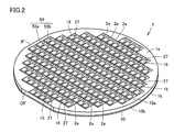
- the silicon carbide wafer 1 is provided with a plurality of semiconductor elements 2a.
- a dicing line 50 is provided on the first main surface 1a side of the silicon carbide wafer 1.
- the dicing line 50 includes a first dicing line 50a extending along a specific direction (for example, ⁇ 1-100> direction) and a direction perpendicular to the specific direction (for example, ⁇ 11-20> direction). And a second dicing line 50b extending along the line.
- Each of the plurality of semiconductor elements 2a is configured to be separable by cutting silicon carbide wafer 1 along dicing line 50, for example.
- the silicon carbide wafer 1 may be provided with an orientation flat OF and an index flat IF.
- the orientation flat OF may extend, for example, along the ⁇ 11-20> direction.
- the index flat IF may extend along the ⁇ 1-100> direction, for example.
- Silicon carbide wafer 1 includes a silicon carbide substrate 10 made of hexagonal silicon carbide.
- the gate electrode 27 and the source electrode 16 are exposed on the surface of each of the plurality of semiconductor elements 2a, and the drain electrode 20 is exposed on the back surface.
- gate electrode 27 and source electrode 16 are exposed on the first main surface 1a side of silicon carbide wafer 1, and drain electrode 20 is exposed on the second main surface 1b side of silicon carbide wafer 1. ing.
- FIG. 3 is a schematic cross-sectional view showing a configuration of semiconductor element 2a in a visual field (sectional view) along a direction parallel to first main surface 1a of silicon carbide wafer 1.
- MOSFET as an example of semiconductor element 2a is, for example, a vertical semiconductor element, and includes silicon carbide substrate 10, gate electrode 27, gate oxide film 15, interlayer insulating film 21, and source. It mainly has an electrode 16 and a drain electrode 20.
- Silicon carbide substrate 10 has a third main surface 10a and a fourth main surface 10b opposite to third main surface 10a, and includes silicon carbide single crystal substrate 11 and silicon carbide single crystal substrate 11. And a silicon carbide epitaxial layer 17 provided on the substrate.
- Silicon carbide single crystal substrate 11 is made of, for example, a polytype 4H hexagonal silicon carbide single crystal.
- the maximum diameter of third main surface 10a of silicon carbide substrate 10 is, for example, larger than 100 mm, preferably 150 mm or more.
- Third main surface 10a of silicon carbide substrate 10 is, for example, a surface that is off by 4 ° or less from the ⁇ 0001 ⁇ plane or ⁇ 0001 ⁇ plane.
- the third main surface 10a is, for example, a surface that is off by about 4 ° or less from the (0001) surface or the (0001) surface
- the fourth main surface 10b is a (000-1) surface or ( 000-1) is a surface that is off by about 4 ° or less from the surface.
- Silicon carbide substrate 10 has a thickness of, for example, 600 ⁇ m or less, and preferably 300 ⁇ m or less.
- Silicon carbide epitaxial layer 17 has drift region 12, body region 13, source region 14, and contact region 18.
- Drift region 12 is an n-type (first conductivity type) region containing an n-type impurity such as nitrogen, for example.
- the concentration of the n-type impurity in the drift region 12 is, for example, about 5.0 ⁇ 10 15 cm ⁇ 3 .
- Body region 13 is a p-type (second conductivity type) region containing a p-type impurity such as Al (aluminum) or B (boron).
- the concentration of the p-type impurity contained in body region 13 is, for example, about 1 ⁇ 10 17 cm ⁇ 3 .
- the source region 14 is an n-type region containing an n-type impurity such as phosphorus.
- the source region 14 is formed so as to be surrounded by the body region 13 in a visual field (plan view) viewed along a direction perpendicular to the third main surface 10a.
- the concentration of the n-type impurity included in the source region 14 is higher than the concentration of the n-type impurity included in the drift region 12.
- the concentration of the n-type impurity contained in the source region 14 is, for example, 1 ⁇ 10 20 cm ⁇ 3 .
- Source region 14 is separated from drift region 12 by body region 13.
- Contact region 18 is a p-type region containing a p-type impurity such as aluminum.
- the contact region 18 is provided so as to be surrounded by the source region 14 in plan view.
- Contact region 18 is in contact with body region 13.
- the concentration of the p-type impurity contained in the contact region 18 is higher than the concentration of the p-type impurity contained in the body region 13.
- the concentration of the p-type impurity contained in contact region 18 is, for example, 1 ⁇ 10 20 cm ⁇ 3 .
- Gate oxide film 15 is formed in contact with third main surface 10a of silicon carbide substrate 10 so as to extend from the upper surface of one source region 14 to the upper surface of the other source region 14. Gate oxide film 15 is in contact with source region 14, body region 13, and drift region 12 at third main surface 10 a of silicon carbide substrate 10. Gate oxide film 15 is made of, for example, silicon dioxide. The thickness of the gate oxide film 15 is, for example, about 40 nm to 60 nm.
- the gate electrode 27 is disposed in contact with the gate oxide film 15 so as to extend from one source region 14 to the other source region 14. Gate electrode 27 is provided on gate oxide film 15 so as to sandwich gate oxide film 15 between silicon carbide substrate 10. Gate electrode 27 is formed in source region 14, body region 13 and drift region 12 with gate oxide film 15 interposed.
- the gate electrode 27 is made of a conductor such as polysilicon doped with impurities.
- the source electrode 16 has a source electrode portion 16a and a surface protective electrode 16b.
- Source electrode portion 16 a is in contact with source region 14 and contact region 18 on third main surface 10 a of silicon carbide substrate 10.
- Source electrode portion 16a includes, for example, TiAlSi.
- source electrode portion 16 a is in ohmic contact with each of source region 14 and contact region 18.
- the surface protection electrode 16 b is in direct contact with the source electrode portion 16 a and is provided so as to cover the interlayer insulating film 21.
- the surface protection electrode 16 b is electrically connected to the source region 14 through the source electrode 16.
- the interlayer insulating film 21 is provided in contact with each of the gate electrode 27 and the gate oxide film 15 so as to cover the gate electrode 27.
- the interlayer insulating film 21 electrically insulates the gate electrode 27 and the source electrode 16 from each other.
- Interlayer insulating film 21 is made of, for example, silicon dioxide.
- the drain electrode 20 includes a drain electrode portion 20a and a back surface protection electrode 20b. Drain electrode portion 20 a is provided in contact with fourth main surface 10 b of silicon carbide substrate 10. Drain electrode portion 20a is made of a material such as NiSi (nickel silicide) capable of ohmic contact with n-type silicon carbide single crystal substrate 11. The back surface protection electrode 20b is electrically connected to the drain electrode portion 20a.
- NiSi nickel silicide
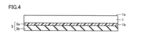
- Adhesive tape 3 is attached to, for example, second main surface 1 b of silicon carbide wafer 1.
- Adhesive tape 3 may be attached to first main surface 1a of silicon carbide wafer 1. That is, adhesive tape 3 is attached to one surface of first main surface 1a and second main surface 1b of silicon carbide wafer 1.
- the pressure-sensitive adhesive tape has a pressure-sensitive adhesive portion 3a that is in contact with one surface of the first main surface 1a and the second main surface 1b, and a base material 3b that is located on the opposite side to the one surface when viewed from the pressure-sensitive adhesive portion 3a.
- the adhesive part 3a for example, an acrylic adhesive having adhesiveness can be used.
- the substrate 3b for example, an organic compound such as polyester can be used.
- the adhesive portion 3a a material whose adhesive strength is reduced by irradiating energy rays such as ultraviolet rays may be used. Examples of the material whose adhesive strength is reduced by irradiating energy rays such as ultraviolet rays include ultraviolet curable resins.
- a material whose adhesive strength is reduced by being heated may be used as the adhesive portion 3a. An example of a material whose adhesive strength is reduced by being heated is a thermosetting resin.
- the step of attaching the adhesive tape (S20: FIG. 1) is performed after the step of preparing the silicon carbide wafer (S10: FIG. 1) and before the first cutting step (S30: FIG. 1).
- the dicing device 30 mainly includes a blade 4, a horn 5, a first shaft 6, a second shaft 7, an ultrasonic spindle 8, and a motor 9.
- the blade 4 is fixed by being sandwiched between horns 5.
- the width W of the blade 4 is, for example, not less than 50 ⁇ m and not more than 100 ⁇ m.
- the horn 5 is connected to the first shaft 6.
- the first shaft 6 is connected to the second shaft 7.
- the second shaft 7 is connected to the ultrasonic spindle 8.
- the ultrasonic spindle 8 vibrates in a direction perpendicular to the rotation surface of the blade 4 (x direction).
- the blade 4 As the ultrasonic spindle 8 vibrates in the x direction, the blade 4 repeatedly contracts and extends in the x direction. Thereby, the blade 4 repeats contraction and extension in a direction parallel to the rotation surface of the blade 4 (z direction).
- the motor 9 is connected to the second shaft 7 and is configured to rotate the blade 4. As shown in FIG. 6, the blade 4 is configured to be rotatable in the rotation direction R around the second shaft 7.
- the blade 4 contacts the silicon carbide wafer 1 while rotating around the second shaft 7, whereby the silicon carbide wafer 1 is cut.
- silicon carbide wafer 1 is cut by rotating blade 4.
- Blade 4 penetrates silicon carbide wafer 1 and adhesive portion 3a and cuts a part of base material 3b.
- the cut 3b1 is formed in the base material 3b.
- the depth D of the cut 3b is, for example, 15% or more and 50% or less of the thickness H of the substrate 3b, and preferably 20% or more and 30% or less of the thickness H of the substrate 3b.
- the cutting speed of silicon carbide wafer 1 in the direction parallel to first main surface 1a of silicon carbide wafer 1 is not less than 1 mm / second and not more than 40 mm / second, more preferably 10 mm / second. 2 seconds or more and 20 mm / second or less.
- the cutting speed of silicon carbide wafer 1 is determined by dividing the cutting distance in the cutting direction parallel to first main surface 1a of silicon carbide wafer 1 by the cutting time.
- the rotational speed of the blade 4 is 5000 rpm or more and 50000 rpm or less, and more preferably 8000 rpm or more and 20000 rpm or less.
- silicon carbide wafer 1 moves, for example, in a direction parallel to the rotating surface of blade 4. Thereby, silicon carbide wafer 1 is cut from one end to the other end of first main surface 1a in plan view.
- one of silicon carbide wafer 1 and blade 4 moves relative to the other.
- silicon carbide wafer 1 is cut by fixing blade 4 in first main surface 1a of silicon carbide wafer 1 and moving silicon carbide wafer 1 in a direction parallel to first main surface 1a. Also good.
- silicon carbide wafer 1 is cut by fixing silicon carbide wafer 1 in first main surface 1a of silicon carbide wafer 1 and moving blade 4 in a direction parallel to first main surface 1a. May be.
- silicon carbide wafer 1 is cut along a plane substantially parallel to the ⁇ 11-20 ⁇ plane.
- silicon carbide wafer 1 is cut substantially along the ⁇ 1-100> direction.
- silicon carbide wafer 1 is cut along a plane substantially parallel to any one of (11-20) plane, (-2110) plane and (1-210) plane.
- the Each of the (11-20) plane, the (-2110) plane, and the (1-210) plane is a crystallographically equivalent plane.
- silicon carbide wafer 1 is cut along a direction substantially parallel to either the [1-100] direction or the [ ⁇ 1100] direction.
- the (11-20) plane is a plane perpendicular to the [11-20] direction.
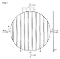
- Silicon carbide wafer 1 may be cut. Conversely, silicon carbide wafer 1 may be cut from the orientation flat OF side toward the opposite side of orientation flat OF. As shown in FIG. 7, the entire silicon carbide wafer 1 is cut with a predetermined width. Thereby, a plurality of strip-shaped pieces 1c are formed as viewed along the direction perpendicular to the first main surface 1a.
- the major axis direction of each of the plurality of pieces 1c is, for example, a direction parallel to the direction in which the index flat IF extends.
- the short axis direction of each of the plurality of pieces 1c is, for example, a direction parallel to the direction in which the orientation flat OF extends.
- the second cutting step (S40: FIG. 1) is performed.
- the silicon carbide wafer along a plane substantially perpendicular to the ⁇ 11-20 ⁇ plane and substantially perpendicular to the first main surface 1a. 1 is cut.
- silicon carbide wafer 1 is cut substantially along the ⁇ 11-20> direction.
- silicon carbide wafer 1 is cut along a plane substantially parallel to the ⁇ 1-100 ⁇ plane.
- silicon carbide wafer 1 is cut along a plane substantially parallel to any one of (1-100) plane, (01-10) plane and (-1010) plane.
- the Each of the (1-100) plane, the (01-10) plane, and the (-1010) plane is a crystallographically equivalent plane.
- silicon carbide wafer 1 is cut along a direction substantially parallel to either the [11-20] direction or the [-1-120] direction.
- the (1-100) plane is a plane perpendicular to the [1-100] direction.
- the blade 4 comes into contact with the silicon carbide wafer 1 while rotating around the second shaft 7. Is disconnected.
- silicon carbide wafer 1 is cut by rotating blade 4.
- Blade 4 penetrates silicon carbide wafer 1 and adhesive portion 3a and cuts a part of base material 3b.
- the cut 3b1 is formed in the base material 3b.
- the depth D of the cut 3b is, for example, 15% or more and 50% or less of the thickness H of the substrate 3b, and preferably 20% or more and 30% or less of the thickness H of the substrate 3b.
- the cutting speed of silicon carbide wafer 1 in the direction parallel to first main surface 1a of silicon carbide wafer 1 is not less than 1 mm / second and not more than 40 mm / second, more preferably 10 mm / second. 2 seconds or more and 20 mm / second or less.
- the cutting speed of silicon carbide wafer 1 is determined by dividing the cutting distance in the cutting direction parallel to first main surface 1a of silicon carbide wafer 1 by the cutting time.
- the rotation speed of the blade 4 is 5000 rpm or more and 50000 rpm or less, and more preferably 8000 rpm or more and 20000 rpm or less.
- silicon carbide is moved from index flat IF to direction CH ⁇ b> 2 that faces away from index flat IF when viewed from the center of first main surface 1 a of silicon carbide wafer 1.
- the wafer 1 may be cut.
- silicon carbide wafer 1 may be cut from the side opposite to index flat IF as viewed from the center of first main surface 1a of silicon carbide wafer 1 toward the index flat IF side.
- all of the plurality of pieces 1c are cut with a predetermined width. Thereby, a plurality of chips 1d are formed.
- outer shape of chip 1d is, for example, a quadrangle, and preferably a rectangle or a square.
- first main surface 1a of silicon carbide wafer 1 may be a surface that is off by 3 ° or more and 5 ° or less from the ⁇ 0001 ⁇ plane toward the off direction.
- third main surface 10a of silicon carbide substrate 10 included in silicon carbide wafer 1 is a surface that is off by 3 ° or more and 5 ° or less from the ⁇ 0001 ⁇ plane in the off direction.
- silicon carbide wafer 1 is cut substantially in the off direction.
- the plane indicated by a broken line is the ⁇ 0001 ⁇ plane, preferably the (0001) plane.
- the direction C1 is the ⁇ 0001> direction, preferably the [0001] direction.
- Third main surface 10a of silicon carbide substrate 10 is, for example, a surface that is off by an off angle ⁇ from a ⁇ 0001 ⁇ plane (a surface indicated by a broken line).
- direction C ⁇ b> 2 is a direction perpendicular to third main surface 10 a of silicon carbide substrate 10.
- the off direction is a direction in which the direction C1 is inclined in the direction C2.
- the off direction is the ⁇ 11-20> direction.
- the step of removing the adhesive tape (S50: FIG. 1) is performed.
- the adhesive part 3a of the adhesive tape 3 is made of a material whose adhesive strength is reduced by irradiating ultraviolet rays
- the adhesive part 3a is irradiated with ultraviolet light.
- the chip 1 d is removed from the adhesive portion 3 a of the adhesive tape 3.
- Chip 1 d includes at least one or more semiconductor elements 2 a and constitutes silicon carbide semiconductor device 2.
- MOSFET 2 as silicon carbide semiconductor device 2 includes a silicon carbide substrate 10, a source electrode 16, a gate electrode 27, and a drain electrode 20.
- the first cutting step (S30: FIG. 1) and the second cutting step (S40: FIG. 1) may be alternately repeated.
- the first cutting step D1 silicon carbide wafer 1 is cut along a plane substantially parallel to the ⁇ 11-20 ⁇ plane. Silicon carbide wafer 1 is cut, for example, from the orientation flat OF side toward the opposite side of orientation flat OF. Thereby, silicon carbide wafer 1 is separated into two pieces.
- the second cutting step D2 silicon carbide wafer 1 is formed along a plane that is substantially perpendicular to the ⁇ 11-20 ⁇ plane and substantially perpendicular to first main surface 1a. Disconnected. Silicon carbide wafer 1 is cut from index flat IF in a direction toward the opposite side of index flat IF when viewed from the center of first main surface 1a of silicon carbide wafer 1. Thereby, silicon carbide wafer 1 is separated into four pieces.
- silicon carbide wafer 1 is cut along a plane substantially parallel to the ⁇ 11-20 ⁇ plane.
- the silicon carbide wafer 1 is cut, for example, from the orientation flat OF side toward the opposite side of the orientation flat OF at a position shifted from the region cut in the first cutting step by, for example, a distance on the index flat IF side.
- silicon carbide wafer 1 is separated into six pieces.
- silicon carbide wafer 1 is formed along a plane that is substantially perpendicular to the ⁇ 11-20 ⁇ plane and substantially perpendicular to first main surface 1a. Disconnected.
- silicon carbide wafer 1 is moved from index flat IF to first main surface 1a of silicon carbide wafer 1. It is cut in the direction toward the opposite side of the index flat IF when viewed from the center.
- silicon carbide wafer 1 may be cut by alternately repeating the first cutting step and the second cutting step.
- the second cutting step may be performed a plurality of times.
- the first conductivity type is n-type and the second conductivity type is p-type.
- the first conductivity type is p-type and the second conductivity type is n-type. It is good.
- a planar MOSFET has been described as an example of the semiconductor element, the semiconductor element may be a trench MOSFET.
- the semiconductor element may be a diode, an IGBT (Insulated Gate Bipolar Transistor), a JFET (Junction Field Effect Transistor), or the like.
- a first cutting step is performed in which silicon carbide wafer 1 is cut along a plane substantially parallel to the ⁇ 11-20 ⁇ plane.
- Second cutting step in which silicon carbide wafer 1 is cut along a plane substantially perpendicular to the ⁇ 11-20 ⁇ plane and substantially perpendicular to the first main surface after the first cutting step. Is done.
- the silicon carbide wafer 1 is not cut using the cleavage plane, but the silicon carbide wafer 1 is mechanically cut with the blade to form the chip, so that the chip is caught in the blade. Occurrence of chipping can be suppressed.
- first main surface 1a is a surface that is turned off by 3 ° or more and 5 ° or less from the ⁇ 0001 ⁇ plane in the off direction.
- silicon carbide wafer 1 is cut substantially in the off direction.
- the method for manufacturing MOSFET 2 cuts silicon carbide wafer 1 in the direction parallel to first main surface 1a in each of the first cutting step and the second cutting step. Is 1 mm / second or more and 40 mm / second or less. Since the force with respect to the silicon carbide wafer 1 can be reduced by setting the cutting speed of the silicon carbide wafer 1 to 1 mm / second or more, it is possible to suppress the chip 1 d from being caught in the blade 4. By setting the cutting speed of silicon carbide wafer 1 to 40 mm / second or less, deterioration of blade 4 can be suppressed.
- silicon carbide wafer 1 is cut by rotating blade 4 in each of the first cutting step and the second cutting step.
- the rotation speed of the blade 4 is 5000 rpm or more and 50000 rpm or less. Since the force with respect to the silicon carbide wafer 1 can be reduced by setting the rotational speed of the blade 4 to 5000 rpm or more, it is possible to suppress the chip 1 d from being caught in the blade 4. By setting the rotation speed of the blade 4 to 50000 rpm or less, the deterioration of the blade 4 can be suppressed.
- the manufacturing method of MOSFET 2 is the first main surface 1a and second main surface 1b after the step of preparing silicon carbide wafer 1 and before the first cutting step.
- the method further includes the step of affixing the adhesive tape 3 to one of the surfaces.
- the pressure-sensitive adhesive tape 3 has a pressure-sensitive adhesive portion 3a that is in contact with one surface and a base material 3b that is located on the opposite side of the one surface as viewed from the pressure-sensitive adhesive portion 3a.
- a cut 3b1 having a depth of 15% or more and 50% or less of the thickness of the substrate 3b is formed in the substrate.
- the manufacturing method of MOSFET 2 according to the present embodiment is perpendicular to the first main surface by cutting silicon carbide wafer 1 with a predetermined width in the first cutting process.
- a plurality of strip-shaped pieces 1c are formed when viewed along a different direction.
- a plurality of chips 1d are formed by cutting all of the plurality of pieces 1c with a predetermined width.
- the first cutting step and the second cutting step are alternately repeated according to the following steps.
- the chip 1d having an arbitrary size can be formed by an arbitrary cutting method, the degree of freedom of the cutting method can be increased.
- the occurrence rate of chipping when silicon carbide wafer 1 is cut by the cutting method according to the example is compared.
- the occurrence rate of chipping when silicon carbide wafer 1 was cut by the cutting method according to the example was compared.
- the silicon carbide wafer 1 is cut at a predetermined pitch along a direction perpendicular to the [11-20] direction (first cutting step), whereby a plurality of strip-shaped pieces are cut. Formed.
- a plurality of chips were formed by cutting the strip-shaped pieces at a predetermined pitch along the direction parallel to the [11-20] direction (second cutting step).
- a total of 42 silicon carbide wafers 1 were cut using the cutting method according to the example. Each silicon carbide wafer 1 was observed with an optical microscope to confirm whether chipping occurred on the chip. The chip arrangement parallel to the cut surface in the second cutting step was taken as one line, and all the chips were observed every 5 lines. When one or more chippings were observed in the first main surface 1a of the silicon carbide wafer 1, it was determined that the chipping occurred.
- the cutting method according to the comparative example by cutting the silicon carbide wafer 1 at a predetermined pitch along the direction parallel to the [11-20] direction (second cutting step), a plurality of strip-shaped fragments are obtained. Formed. Next, a plurality of chips were formed by cutting the strip-shaped pieces along a direction perpendicular to the [11-20] direction at a predetermined pitch (first cutting step). A total of 11 silicon carbide wafers 1 were cut using the cutting method according to the comparative example. Each silicon carbide wafer 1 was observed with an optical microscope to confirm whether chipping occurred on the chip. The chip arrangement parallel to the cut surface in the first cutting step was taken as one line, and all the chips were observed every 5 lines. When one or more chippings were observed in the first main surface 1a of the silicon carbide wafer 1, it was determined that the chipping occurred.
- Table 1 shows the relationship between the silicon carbide wafer cutting method and the occurrence rate of chipping.
- the silicon carbide wafer 1 was first cut along the direction parallel to the [11-20] direction (second cutting step), and then silicon carbide was cut along the direction perpendicular to the [11-20] direction.
- second cutting step the cutting method of cutting the wafer 1
- first cutting step after cutting the silicon carbide wafer 1 along the direction perpendicular to the [11-20] direction (first cutting step)
- second cutting step can greatly reduce the occurrence rate of chipping.
Landscapes
- Engineering & Computer Science (AREA)
- Mechanical Engineering (AREA)
- Dicing (AREA)
- Chemical & Material Sciences (AREA)
- Crystallography & Structural Chemistry (AREA)
Abstract
MOSFET(2)の製造方法は以下の工程によれば、{11-20}面に実質的に平行な面に沿って炭化珪素ウェハ(1)が切断される第1切断工程が行われる。第1切断工程後、{11-20}面に対して実質的に垂直でかつ第1の主面に対して実質的に垂直な面に沿って炭化珪素ウェハ(1)が切断される第2切断工程が行われる。
Description
本発明は、炭化珪素半導体装置の製造方法に関する。
近年、半導体装置の高耐圧化、低損失化、高温環境下での使用などを可能とするため、半導体装置を構成する材料として炭化珪素の採用が進められつつある。
たとえば特開2014-86446号公報(特許文献1)には、炭化珪素ウェハの切断方法が記載されている。当該炭化珪素ウェハの切断方法によれば、c面上において{1-210}面が構成する直線と垂直な方向に沿って炭化珪素ウェハが切断された後、c面上において{1-210}面と平行な方向に沿って炭化珪素ウェハが切断される。
しかしながら、当該炭化珪素ウェハの切断方法を用いた場合であっても、チッピングの発生を抑制することは困難であった。
本発明の一態様の目的は、チッピングの発生を抑制することができる炭化珪素半導体装置の製造方法を提供することである。
本発明の一態様に係る炭化珪素半導体装置の製造方法は以下の工程を備えている。第1の主面と、第1の主面と反対側の第2の主面とを有する炭化珪素ウェハが準備される。{11-20}面に実質的に平行な面に沿って炭化珪素ウェハが切断される第1切断工程が行われる。第1切断工程後、{11-20}面に対して実質的に垂直でかつ第1の主面に対して実質的に垂直な面に沿って炭化珪素ウェハが切断される第2切断工程が行われる。
本発明の一態様によれば、チッピングの発生を抑制することができる炭化珪素半導体装置の製造方法を提供することができる。
[本発明の実施形態の説明]
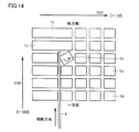
本発明者らは、チッピングが発生する原因について以下のような検討を行った。まず、特開2014-86446号公報に記載の方法と同様の方法を用いて炭化珪素ウェハをダイシングすることにより複数のチップを形成した。具体的には、まず、炭化珪素ウェハの裏面全面に粘着テープを貼り付けた。次に、図14に示されるように、第1切断工程において、ブレード4を用いて、[11-20]方向CH1に沿って炭化珪素ウェハ全体を所定の幅で切断し、複数の短冊状の断片1cを形成した。次に、第2切断工程において、ブレード4を用いて、[11-20]方向に対して垂直な[1-100]方向CH2に沿って複数の短冊状の断片1cの各々を所定の幅で切断し、複数のチップ1dを形成した。なお、第2切断工程における炭化珪素ウェハの切断面は、六方晶炭化珪素の劈開面である{11-20}面である。また第1切断工程および第2切断工程の各々において、炭化珪素ウェハはブレードによって炭化珪素ウェハの厚み方向に完全に切断されるが、粘着テープは厚み方向において一部のみが切断されるだけで完全には切断されない。粘着テープは、炭化珪素ウェハが切断されて形成されるチップが飛び散らないようにチップの各々を保持している。
本発明者らは、チッピングが発生する原因について以下のような検討を行った。まず、特開2014-86446号公報に記載の方法と同様の方法を用いて炭化珪素ウェハをダイシングすることにより複数のチップを形成した。具体的には、まず、炭化珪素ウェハの裏面全面に粘着テープを貼り付けた。次に、図14に示されるように、第1切断工程において、ブレード4を用いて、[11-20]方向CH1に沿って炭化珪素ウェハ全体を所定の幅で切断し、複数の短冊状の断片1cを形成した。次に、第2切断工程において、ブレード4を用いて、[11-20]方向に対して垂直な[1-100]方向CH2に沿って複数の短冊状の断片1cの各々を所定の幅で切断し、複数のチップ1dを形成した。なお、第2切断工程における炭化珪素ウェハの切断面は、六方晶炭化珪素の劈開面である{11-20}面である。また第1切断工程および第2切断工程の各々において、炭化珪素ウェハはブレードによって炭化珪素ウェハの厚み方向に完全に切断されるが、粘着テープは厚み方向において一部のみが切断されるだけで完全には切断されない。粘着テープは、炭化珪素ウェハが切断されて形成されるチップが飛び散らないようにチップの各々を保持している。
チッピングが発生した複数のチップを光学顕微鏡で観察し、複数のチップの各々においてチッピングが発生した位置を詳細に調査した。その結果、複数のチップの各々において同じ位置でチッピングが発生する傾向があることが判明した。具体的には、ブレード4を用いて炭化珪素ウェハの主面の一方側から他方側に向かって炭化珪素ウェハを切断する場合、チップ1dの他方側の角部において、チッピングが発生する傾向があった。第2切断工程において、六方晶炭化珪素の劈開面である{11-20}面に沿って炭化珪素ウェハを切断すると、炭化珪素ウェハの断片1cをブレード4によって機械的に切断して四角形のチップ1dを形成する前に、劈開面で断片1cが割れて四角形のチップ1dが形成される。当該チップ1dが、回転しているブレード4に巻き込まれることでチップ1dが回転し、チップ1dの他方側の角部において、チッピングが発生すると考えられる。
第1切断工程では、炭化珪素ウェハは複数の短冊状の断片に分断され、第2切断工程では、複数の短冊状の断片の各々が複数のチップに分断される。第1切断工程では、短冊状の断片が広い面積で粘着テープに接して保持されている。そのため、炭化珪素ウェハを切断する際、短冊状の断片がブレードに巻き込まれたとしても短冊状の断片は回転しづらい。一方、第2切断工程では、短冊状の断片が分断されたチップが、短冊状の断片よりも狭い面積で粘着テープに接して保持されている。そのため、短冊上の断片と比較して、チップは粘着テープに強固に固定されていない。それゆえ、炭化珪素ウェハを切断する際、チップがブレードに巻き込まれて回転し易くなると考えられる。
そこで発明者らは、第2切断工程において、劈開面である{11-20}面と実質的に垂直な面で炭化珪素ウェハを切断することにより、劈開性を利用して炭化珪素ウェハを切断するのではなく、ブレードで機械的に炭化珪素ウェハを切断することを考え出した。これにより、ブレードによって炭化珪素ウェハを切断する際、チップがブレードに巻き込まれて回転し、チップにチッピングが発生することを抑制することができる。
次に、本発明の実施態様を列記して説明する。
(1)本発明の一態様に係る炭化珪素半導体装置の製造方法は以下の工程を備えている。第1の主面と、第1の主面と反対側の第2の主面とを有する炭化珪素ウェハが準備される。{11-20}面に実質的に平行な面に沿って炭化珪素ウェハが切断される第1切断工程が行われる。第1切断工程後、{11-20}面に対して実質的に垂直でかつ第1の主面に対して実質的に垂直な面に沿って炭化珪素ウェハが切断される第2切断工程が行われる。なお、{11-20}面に実質的に平行な面とは、{11-20}面が、たとえば5°以内の角度だけ傾いた面のことである。{11-20}面に対して実質的に垂直な面は、{11-20}面に対して垂直な面が、たとえば5°以内の角度だけ傾いた面のことである。第1の主面に対して実質的に垂直な面とは、第1の主面に対して垂直な面が、たとえば5°以内の角度だけ傾いた面のことである。これにより、第2切断工程において、劈開面を利用して炭化珪素ウェハを切断するのではなくブレードで機械的に炭化珪素ウェハを切断してチップを形成することにより、チップがブレードに巻き込まれることでチッピングが発生することを抑制することができる。
(1)本発明の一態様に係る炭化珪素半導体装置の製造方法は以下の工程を備えている。第1の主面と、第1の主面と反対側の第2の主面とを有する炭化珪素ウェハが準備される。{11-20}面に実質的に平行な面に沿って炭化珪素ウェハが切断される第1切断工程が行われる。第1切断工程後、{11-20}面に対して実質的に垂直でかつ第1の主面に対して実質的に垂直な面に沿って炭化珪素ウェハが切断される第2切断工程が行われる。なお、{11-20}面に実質的に平行な面とは、{11-20}面が、たとえば5°以内の角度だけ傾いた面のことである。{11-20}面に対して実質的に垂直な面は、{11-20}面に対して垂直な面が、たとえば5°以内の角度だけ傾いた面のことである。第1の主面に対して実質的に垂直な面とは、第1の主面に対して垂直な面が、たとえば5°以内の角度だけ傾いた面のことである。これにより、第2切断工程において、劈開面を利用して炭化珪素ウェハを切断するのではなくブレードで機械的に炭化珪素ウェハを切断してチップを形成することにより、チップがブレードに巻き込まれることでチッピングが発生することを抑制することができる。
(2)上記(1)に係る炭化珪素半導体装置の製造方法において好ましくは、第1の主面は、{0001}面からオフ方向に向かって3°以上5°以下オフした面である。第2切断工程において、炭化珪素ウェハは、実質的にオフ方向に向かって切断される。なお、実質的にオフ方向とは、オフ方向からたとえば5°以内の角度だけ傾いた方向のことである。これにより、表面段差の影響によるブレードの摩耗を避ける事ができ、ブレードの摩耗に伴うブレードのひずみやばりによるチッピングの発生をさらに抑制することができる。
(3)上記(1)または(2)に係る炭化珪素半導体装置の製造方法において好ましくは、第1切断工程および第2切断工程の各々において、第1の主面と平行な方向における炭化珪素ウェハの切断速度は、1mm/秒以上40mm/秒以下である。炭化珪素ウェハの切断速度を1mm/秒以上とすることにより、炭化珪素ウェハに対する力を低減することできるので、チップがブレードに巻き込まれることを抑制することができる。炭化珪素ウェハの切断速度を40mm/秒以下とすることにより、ブレードの劣化を抑制することができる。
(4)上記(1)~(3)のいずれかに係る炭化珪素半導体装置の製造方法において好ましくは、第1切断工程および第2切断工程の各々において、回転するブレードによって炭化珪素ウェハが切断される。ブレードの回転速度は、5000rpm以上50000rpm以下である。ブレードの回転速度を5000rpm以上とすることにより、炭化珪素ウェハに対する力を低減することできるので、チップがブレードに巻き込まれることを抑制することができる。ブレードの回転速度を50000rpm以下とすることにより、ブレードの劣化を抑制することができる。
(5)上記(1)~(4)のいずれかに係る炭化珪素半導体装置の製造方法において好ましくは、炭化珪素ウェハを準備する工程後であり第1切断工程前に、第1の主面および第2の主面の一方の面に粘着テープを貼り付ける工程をさらに備える。粘着テープは、一方の面に接する粘着部と、粘着部から見て一方の面とは反対側に位置する基材とを有する。第1切断工程および第2切断工程の各々において、基材の厚みの15%以上50%以下の深さを有する切り込みが基材に形成される。基材に形成される切り込みの深さを基材の厚みの15%以上とすることにより、炭化珪素ウェハ1において切断されていない箇所が発生することを抑制することができる。基材に形成される切り込みの深さを大きくすると、第1の主面と平行な方向におけるチップとチップとの距離が広がる。そのため、実際の切断位置が予定している切断位置からずれる場合がある。基材に形成される切り込みの深さを基材の厚みの50%以下とすることにより、実際の切断位置が予定している切断位置からずれることを抑制することができる。
(6)上記(1)~(5)のいずれかに係る炭化珪素半導体装置の製造方法において好ましくは、第1切断工程において、炭化珪素ウェハ全体が所定の幅で切断されることにより、第1の主面に対して垂直な方向に沿って見て短冊状の複数の断片が形成される。第2切断工程において、複数の断片の全てが所定の幅で切断されることにより複数のチップが形成される。これにより、短時間で炭化珪素ウェハをチップに分離することができる。
(7)上記(1)~(5)のいずれかに係る炭化珪素半導体装置の製造方法において好ましくは、第1切断工程と、第2切断工程とが交互に繰り返される。これにより、任意のサイズのチップを任意の切断方法により形成することができるので、切断方法の自由度を高めることができる。
[本発明の実施形態の詳細]
以下、図面に基づいて本発明の実施の形態について説明する。なお、以下の図面において同一または相当する部分には同一の参照番号を付しその説明は繰返さない。また、本明細書中の結晶学的記載においては、個別方位を[]、集合方位を<>、個別面を()、集合面を{}でそれぞれ示している。また、負の指数については、結晶学上、”-”(バー)を数字の上に付けることになっているが、本明細書中では、数字の前に負の符号を付けている。
[本発明の実施形態の詳細]
以下、図面に基づいて本発明の実施の形態について説明する。なお、以下の図面において同一または相当する部分には同一の参照番号を付しその説明は繰返さない。また、本明細書中の結晶学的記載においては、個別方位を[]、集合方位を<>、個別面を()、集合面を{}でそれぞれ示している。また、負の指数については、結晶学上、”-”(バー)を数字の上に付けることになっているが、本明細書中では、数字の前に負の符号を付けている。
本発明の実施の形態に係る炭化珪素半導体装置の一例としてのMOSFET(Metal Oxide Semiconductor Field Effect Transistor)の製造方法について説明する。
最初に炭化珪素ウェハを準備する工程(S10:図1)が実施される。図2に示されるように、第1の主面1aと、第1の主面1aと反対側の第2の主面1bとを有する炭化珪素ウェハ1が準備される。炭化珪素ウェハ1には、複数の半導体素子2aが設けられている。炭化珪素ウェハ1の第1の主面1a側には、ダイシングライン50が設けられている。ダイシングライン50は、ある特定の方向(たとえば<1-100>方向)に沿って延在する第1ダイシングライン50aと、ある特定の方向に対して垂直な方向(たとえば<11-20>方向)に沿って延在する第2ダイシングライン50bとを含む。複数の半導体素子2aの各々は、たとえばダイシングライン50に沿って炭化珪素ウェハ1を切断することにより分離可能に構成されている。
炭化珪素ウェハ1には、オリエンテーションフラットOFと、インデックスフラットIFとが設けられていてもよい。オリエンテーションフラットOFは、たとえば<11-20>方向に沿って延在していてもよい。インデックスフラットIFは、たとえば<1-100>方向に沿って延在していてもよい。炭化珪素ウェハ1は、六方晶炭化珪素から構成された炭化珪素基板10を含んでいる。複数の半導体素子2aの各々の表面には、たとえばゲート電極27とソース電極16とが露出しており、裏面にはドレイン電極20が露出している。言い換えれば、ゲート電極27およびソース電極16は、炭化珪素ウェハ1の第1の主面1a側に露出しており、ドレイン電極20は、炭化珪素ウェハ1の第2の主面1b側に露出している。
次に、半導体素子2aの一例としてのMOSFETの構成について説明する。
図3は、炭化珪素ウェハ1の第1の主面1aに平行な方向に沿った視野(断面視)における、半導体素子2aの構成を示す断面模式図である。図3に示されるように、半導体素子2aの一例としてのMOSFETは、たとえば縦型半導体素子であり、炭化珪素基板10と、ゲート電極27と、ゲート酸化膜15と、層間絶縁膜21と、ソース電極16と、ドレイン電極20とを主に有している。炭化珪素基板10は、第3の主面10aと、第3の主面10aと反対側の第4の主面10bとを有し、炭化珪素単結晶基板11と、炭化珪素単結晶基板11上に設けられた炭化珪素エピタキシャル層17とを主に含む。
図3は、炭化珪素ウェハ1の第1の主面1aに平行な方向に沿った視野(断面視)における、半導体素子2aの構成を示す断面模式図である。図3に示されるように、半導体素子2aの一例としてのMOSFETは、たとえば縦型半導体素子であり、炭化珪素基板10と、ゲート電極27と、ゲート酸化膜15と、層間絶縁膜21と、ソース電極16と、ドレイン電極20とを主に有している。炭化珪素基板10は、第3の主面10aと、第3の主面10aと反対側の第4の主面10bとを有し、炭化珪素単結晶基板11と、炭化珪素単結晶基板11上に設けられた炭化珪素エピタキシャル層17とを主に含む。
炭化珪素単結晶基板11は、たとえばポリタイプ4Hの六方晶炭化珪素単結晶からなる。炭化珪素基板10の第3の主面10aの最大径は、たとえば100mmより大きく、好ましくは150mm以上である。炭化珪素基板10の第3の主面10aは、たとえば{0001}面または{0001}面から4°以下オフした面である。具体的には、第3の主面10aは、たとえば(0001)面または(0001)面から4°以下程度オフした面であり、第4の主面10bは、(000-1)面または(000-1)面から4°以下程度オフした面である。炭化珪素基板10の厚みは、たとえば600μm以下であり、好ましくは300μm以下である。
炭化珪素エピタキシャル層17は、ドリフト領域12と、ボディ領域13と、ソース領域14と、コンタクト領域18とを有している。ドリフト領域12は、たとえば窒素などのn型不純物を含むn型(第1導電型)領域である。ドリフト領域12におけるn型不純物の濃度は、たとえば5.0×1015cm-3程度である。ボディ領域13は、たとえばAl(アルミニウム)またはB(ホウ素)などのp型不純物を含むp型(第2導電型)領域である。ボディ領域13に含まれるp型不純物の濃度は、たとえば1×1017cm-3程度である。
ソース領域14は、リンなどのn型不純物を含むn型領域である。ソース領域14は、第3の主面10aに対して垂直な方向に沿って見た視野(平面視)において、ボディ領域13に取り囲まれるように形成されている。ソース領域14が含むn型不純物の濃度は、ドリフト領域12が含むn型不純物の濃度よりも高い。ソース領域14が含むn型不純物の濃度はたとえば1×1020cm-3である。ソース領域14は、ボディ領域13によりドリフト領域12と隔てられている。
コンタクト領域18は、アルミニウムなどのp型不純物を含むp型領域である。コンタクト領域18は、平面視においてソース領域14に囲まれて設けられている。コンタクト領域18は、ボディ領域13に接している。コンタクト領域18が含むp型不純物の濃度は、ボディ領域13が含むp型不純物の濃度よりも高い。コンタクト領域18が含むp型不純物の濃度はたとえば1×1020cm-3である。
ゲート酸化膜15は、一方のソース領域14の上部表面から他方のソース領域14の上部表面にまで延在するように炭化珪素基板10の第3の主面10aに接して形成されている。ゲート酸化膜15は、炭化珪素基板10の第3の主面10aにおいてソース領域14、ボディ領域13およびドリフト領域12に接している。ゲート酸化膜15は、たとえば二酸化珪素から構成されている。ゲート酸化膜15の厚みは、たとえば40nm以上60nm以下程度である。
ゲート電極27は、一方のソース領域14上から他方のソース領域14上にまで延在するように、ゲート酸化膜15に接触して配置されている。ゲート電極27は、炭化珪素基板10との間にゲート酸化膜15を挟むようにゲート酸化膜15上に設けられている。ゲート電極27は、ソース領域14、ボディ領域13およびドリフト領域12にゲート酸化膜15を介して形成されている。ゲート電極27は、たとえば不純物がドーピングされたポリシリコンなどの導電体から構成されている。
ソース電極16は、ソース電極部16aと表面保護電極16bと有する。ソース電極部16aは、炭化珪素基板10の第3の主面10aにおいてソース領域14およびコンタクト領域18と接する。ソース電極部16aは、たとえばTiAlSiを含む。好ましくは、ソース電極部16aは、ソース領域14およびコンタクト領域18の各々とオーミック接合している。表面保護電極16bは、ソース電極部16aと直接接触しており、層間絶縁膜21を覆うように設けられている。表面保護電極16bは、ソース電極16を介してソース領域14と電気的に接続されている。
層間絶縁膜21は、ゲート電極27を覆うようにゲート電極27およびゲート酸化膜15の各々に接して設けられている。層間絶縁膜21は、ゲート電極27とソース電極16とを電気的に絶縁している。層間絶縁膜21は、たとえば二酸化珪素により構成されている。
ドレイン電極20は、ドレイン電極部20aと、裏面保護電極20bとを含む。ドレイン電極部20aは、炭化珪素基板10の第4の主面10bに接して設けられている。ドレイン電極部20aは、n型の炭化珪素単結晶基板11とオーミック接合可能であるNiSi(ニッケルシリサイド)などの材料から構成されている。裏面保護電極20bは、ドレイン電極部20aと電気的に接続されている。
次に、粘着テープを貼り付ける工程(S20:図1)が実施される。図4に示されるように、粘着テープ3は、たとえば炭化珪素ウェハ1の第2の主面1bに貼り付けられる。粘着テープ3は、炭化珪素ウェハ1の第1の主面1aに貼り付けされてもよい。つまり、粘着テープ3は、炭化珪素ウェハ1の第1の主面1aおよび第2の主面1bの一方の面に貼り付けられる。粘着テープは、第1の主面1aおよび第2の主面1bの一方の面に接する粘着部3aと、粘着部3aから見て一方の面とは反対側に位置する基材3bとを有する。
粘着部3aとしては、たとえば粘着性を有するアクリル粘着剤が使用可能である。基材3bとしては、たとえばポリエステルなどの有機化合物が使用可能である。粘着部3aとして、紫外線などのエネルギー線を照射することにより粘着力が低下する材料が用いられてもよい。紫外線などのエネルギー線を照射することにより粘着力が低下する材料としては、たとえば紫外線硬化型樹脂が挙げられる。また、粘着部3aとして、加熱されることにより粘着力が低下する材料が用いられても構わない。加熱されることにより粘着力が低下する材料としては、たとえば熱硬化型樹脂が挙げられる。なお、粘着テープを貼り付ける工程(S20:図1)は、炭化珪素ウェハを準備する工程(S10:図1)後であり、かつ第1切断工程(S30:図1)前に実施される。
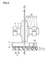
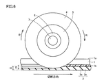
次に、第1切断工程(S30:図1)が実施される。図5に示されるように、ダイシング装置30が準備される。ダイシング装置30は、ブレード4と、ホーン5と、第1軸6と、第2軸7と、超音波スピンドル8と、モータ9とを主に有している。ブレード4は、ホーン5に挟まれて固定されている。ブレード4の幅Wは、たとえば50μm以上100μm以下である。ホーン5は、第1軸6に接続されている。第1軸6は、第2軸7に接続されている。第2軸7は、超音波スピンドル8に接続されている。超音波スピンドル8は、ブレード4の回転面に対して垂直な方向(x方向)に振動する。超音波スピンドル8がx方向に振動することにより、ブレード4がx方向に収縮および伸長を繰り返す。これにより、ブレード4がブレード4の回転面に平行な方向(z方向)に収縮および伸長を繰り返す。モータ9は、第2軸7と接続されておりブレード4を回転可能に構成されている。図6に示されるように、ブレード4は、第2軸7の周りを回転方向Rに回転可能に構成されている。
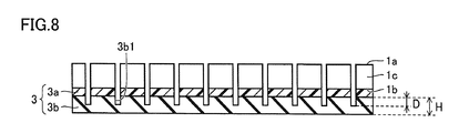
図5および図6に示されるように、第1切断工程において、ブレード4が第2軸7の周りに回転しながら炭化珪素ウェハ1に接触することで、炭化珪素ウェハ1が切断される。言い換えれば、回転するブレード4によって炭化珪素ウェハ1が切断される。ブレード4は、炭化珪素ウェハ1と粘着部3aとを貫通し、基材3bの一部を切断する。言い換えれば、基材3bに切り込み3b1が形成される。切り込み3bの深さDは、たとえば基材3bの厚みHの15%以上50%以下であり、好ましくは、基材3bの厚みHの20%以上30%以下である。
好ましくは、第1切断工程において、炭化珪素ウェハ1の第1の主面1aと平行な方向における炭化珪素ウェハ1の切断速度は、1mm/秒以上40mm/秒以下であり、より好ましくは10mm/秒以上20mm/秒以下である。炭化珪素ウェハ1の切断速度は、炭化珪素ウェハ1の第1の主面1aと平行な切断方向における切断距離を切断時間で除することにより求められる。好ましくは、第1切断工程において、ブレード4の回転速度は、5000rpm以上50000rpm以下であり、より好ましくは、8000rpm以上20000rpm以下である。
図6に示されるように、炭化珪素ウェハ1を切断する工程において、炭化珪素ウェハ1は、たとえばブレード4の回転面と平行な方向に移動する。これにより、平面視における第1の主面1aの一端から他端まで、炭化珪素ウェハ1が切断される。炭化珪素ウェハ1を切断する工程において、炭化珪素ウェハ1およびブレード4の一方が他方に対して移動する。たとえば炭化珪素ウェハ1の第1の主面1a内において、ブレード4を固定し、炭化珪素ウェハ1を第1の主面1aと平行な方向に移動させることにより、炭化珪素ウェハ1が切断されてもよい。反対に、炭化珪素ウェハ1の第1の主面1a内において、炭化珪素ウェハ1を固定し、ブレード4を第1の主面1aと平行な方向に移動させることにより、炭化珪素ウェハ1が切断されてもよい。
図7に示されるように、第1切断工程においては、{11-20}面に実質的に平行な面に沿って炭化珪素ウェハ1が切断される。言い換えれば、実質的に<1-100>方向に沿って炭化珪素ウェハ1が切断される。好ましくは、炭化珪素ウェハ1は、(11-20)面、(-2110)面および(1-210)面のいずれかの面に実質的に平行な面に沿って炭化珪素ウェハ1が切断される。なお、(11-20)面、(-2110)面および(1-210)面の各々は、結晶学的に等価な面である。好ましくは、炭化珪素ウェハ1は、 [1-100]方向および[-1100]方向のいずれかの方向に実質的に平行な方向に沿って切断される。なお、(11-20)面は、[11-20]方向に対して垂直な面である。
図7に示されるように、第1切断工程においては、炭化珪素ウェハ1の第1の主面1aの中心から見て、オリエンテーションフラットOFと反対側から、オリエンテーションフラットOF側に向かう方向CH1に、炭化珪素ウェハ1が切断されてもよい。反対に、オリエンテーションフラットOF側からオリエンテーションフラットOFと反対側に向かって炭化珪素ウェハ1が切断されてもよい。図7に示されるように、炭化珪素ウェハ1全体が所定の幅で切断される。これにより、第1の主面1aに対して垂直な方向に沿って見て短冊状の複数の断片1cが形成される。複数の断片1cの各々の長軸方向は、たとえばインデックスフラットIFが延在する方向と平行な方向である。複数の断片1cの各々の短軸方向は、たとえばオリエンテーションフラットOFが延在する方向と平行な方向である。
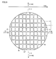
次に、第2切断工程(S40:図1)が実施される。図9に示されるように、第1切断工程後、{11-20}面に対して実質的に垂直でかつ第1の主面1aに対して実質的に垂直な面に沿って炭化珪素ウェハ1が切断される。言い換えれば、実質的に<11-20>方向に沿って炭化珪素ウェハ1が切断される。好ましくは、{1-100}面に実質的に平行な面に沿って炭化珪素ウェハ1が切断される。好ましくは、炭化珪素ウェハ1は、(1-100)面、(01-10)面および(-1010)面のいずれかの面に実質的に平行な面に沿って炭化珪素ウェハ1が切断される。なお、(1-100)面、(01-10)面および(-1010)面の各々は、結晶学的に等価な面である。好ましくは、炭化珪素ウェハ1は、[11-20]方向および[-1-120]方向のいずれかの方向に実質的に平行な方向に沿って切断される。なお、(1-100)面は、[1-100]方向に対して垂直な面である。
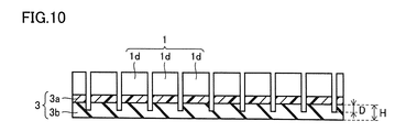
図5、図6、図9および図10に示されるように、第2切断工程において、ブレード4が第2軸7の周りに回転しながら炭化珪素ウェハ1に接触することで、炭化珪素ウェハ1が切断される。言い換えれば、回転するブレード4によって炭化珪素ウェハ1が切断される。ブレード4は、炭化珪素ウェハ1と粘着部3aとを貫通し、基材3bの一部を切断する。言い換えれば、基材3bに切り込み3b1が形成される。切り込み3bの深さDは、たとえば基材3bの厚みHの15%以上50%以下であり、好ましくは、基材3bの厚みHの20%以上30%以下である。
好ましくは、第2切断工程において、炭化珪素ウェハ1の第1の主面1aと平行な方向における炭化珪素ウェハ1の切断速度は、1mm/秒以上40mm/秒以下であり、より好ましくは10mm/秒以上20mm/秒以下である。炭化珪素ウェハ1の切断速度は、炭化珪素ウェハ1の第1の主面1aと平行な切断方向における切断距離を切断時間で除することにより求められる。好ましくは、第2切断工程において、ブレード4の回転速度は、5000rpm以上50000rpm以下であり、より好ましくは、8000rpm以上20000rpm以下である。
図9に示されるように、第2切断工程においては、インデックスフラットIFから、炭化珪素ウェハ1の第1の主面1aの中心から見てインデックスフラットIFと反対側に向かう方向CH2に、炭化珪素ウェハ1が切断されてもよい。反対に、炭化珪素ウェハ1の第1の主面1aの中心から見てインデックスフラットIFと反対側から、インデックスフラットIF側に向かって炭化珪素ウェハ1が切断されてもよい。図9に示されるように、第2切断工程において、複数の断片1c(図7参照)の全てが所定の幅で切断される。これにより、複数のチップ1dが形成される。炭化珪素ウェハ1の第1の主面1aに対して垂直な方向に沿って見て、チップ1dの外形はたとえば四角形であり、好ましくは、長方形または正方形である。
図11に示されるように、炭化珪素ウェハ1の第1の主面1aは、{0001}面からオフ方向に向かって3°以上5°以下オフした面であってもよい。好ましくは、炭化珪素ウェハ1が含む炭化珪素基板10の第3の主面10aは、{0001}面からオフ方向に向かって3°以上5°以下オフした面である。好ましくは、第2切断工程において、炭化珪素ウェハ1は、実質的にオフ方向に向かって切断される。
図11において、破線で示す面は、{0001}面であり、好ましくは(0001)面である。方向C1は、<0001>方向であり、好ましくは[0001]方向である。炭化珪素基板10の第3の主面10aは、たとえば{0001}面(破線で示す面)からオフ角θだけオフした面である。図11において、方向C2は、炭化珪素基板10の第3の主面10aに対して垂直な方向である。オフ方向は、方向C1が方向C2に傾斜する方向である。たとえば、方向C2が、<0001>方向から<11-20>方向に傾斜した方向である場合、オフ方向は<11-20>方向である。
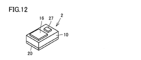
次に、粘着テープを除去する工程(S50:図1)が実施される。たとえば、粘着テープ3の粘着部3aとして、紫外線を照射することにより粘着力が低下する材料が用いられている場合、粘着部3aに紫外性が照射される。これにより、粘着部3aの粘着力が低下する。次に、チップ1dが、粘着テープ3の粘着部3aから取り除かれる。チップ1dは、少なくとも1以上の半導体素子2aを含んでおり、炭化珪素半導体装置2を構成する。以上により炭化珪素半導体装置2の製造が完了する。図12に示されるように、炭化珪素半導体装置2としてのMOSFET2は、炭化珪素基板10と、ソース電極16と、ゲート電極27と、ドレイン電極20とを含む。
次に、本実施の形態の炭化珪素半導体装置の製造方法の変形例について説明する。
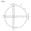
炭化珪素ウェハ1を切断する際に、第1切断工程(S30:図1)と、第2切断工程(S40:図1)とが交互に繰り返されてもよい。図13に示されるように、第1回目の切断工程D1において、{11-20}面に実質的に平行な面に沿って炭化珪素ウェハ1が切断される。炭化珪素ウェハ1は、たとえばオリエンテーションフラットOF側からオリエンテーションフラットOFと反対側に向かって切断される。これにより、炭化珪素ウェハ1は、2つの断片に分離される。次に、第2回目の切断工程D2において、{11-20}面に対して実質的に垂直でかつ第1の主面1aに対して実質的に垂直な面に沿って炭化珪素ウェハ1が切断される。炭化珪素ウェハ1は、インデックスフラットIFから、炭化珪素ウェハ1の第1の主面1aの中心から見てインデックスフラットIFと反対側に向かう方向に切断される。これにより、炭化珪素ウェハ1は、4つの断片に分離される。
炭化珪素ウェハ1を切断する際に、第1切断工程(S30:図1)と、第2切断工程(S40:図1)とが交互に繰り返されてもよい。図13に示されるように、第1回目の切断工程D1において、{11-20}面に実質的に平行な面に沿って炭化珪素ウェハ1が切断される。炭化珪素ウェハ1は、たとえばオリエンテーションフラットOF側からオリエンテーションフラットOFと反対側に向かって切断される。これにより、炭化珪素ウェハ1は、2つの断片に分離される。次に、第2回目の切断工程D2において、{11-20}面に対して実質的に垂直でかつ第1の主面1aに対して実質的に垂直な面に沿って炭化珪素ウェハ1が切断される。炭化珪素ウェハ1は、インデックスフラットIFから、炭化珪素ウェハ1の第1の主面1aの中心から見てインデックスフラットIFと反対側に向かう方向に切断される。これにより、炭化珪素ウェハ1は、4つの断片に分離される。
次に、第3回目の切断工程D3において、{11-20}面に実質的に平行な面に沿って炭化珪素ウェハ1が切断される。第1回目の切断工程において切断された領域から、たとえばインデックスフラットIF側にある距離だけシフトした位置において、炭化珪素ウェハ1は、たとえばオリエンテーションフラットOF側からオリエンテーションフラットOFと反対側に向かって切断される。これにより、炭化珪素ウェハ1は、6つの断片に分離される。次に、第4回目の切断工程D4において、{11-20}面に対して実質的に垂直でかつ第1の主面1aに対して実質的に垂直な面に沿って炭化珪素ウェハ1が切断される。第2回目の切断工程において切断された領域から、たとえばオリエンテーションフラットOF側にある距離だけシフトした位置において、炭化珪素ウェハ1は、インデックスフラットIFから、炭化珪素ウェハ1の第1の主面1aの中心から見てインデックスフラットIFと反対側に向かう方向に切断される。以上のように、第1切断工程と、第2切断工程とが交互に繰り返されて、炭化珪素ウェハ1が切断されてもよい。また第1切断工程が複数回実施された後に、第2切断工程が複数回実施されてもよい。
なお、上記実施の形態において、第1導電型はn型であり、かつ第2導電型はp型であるとして説明したが、第1導電型をp型とし、かつ第2導電型をn型としてもよい。半導体素子の一例として平面型MOSFETを例に挙げて説明したが、半導体素子はトレンチ型MOSFETであってもよい。また半導体素子は、ダイオード、IGBT(Insulated Gate Bipolar Transistor)およびJFET(Junction Field Effect Transistor)などであってもよい。
次に、本実施の形態に係る炭化珪素半導体装置の製造方法の作用効果について説明する。
本実施の形態に係るMOSFET2の製造方法は以下の工程によれば、{11-20}面に実質的に平行な面に沿って炭化珪素ウェハ1が切断される第1切断工程が行われる。第1切断工程後、{11-20}面に対して実質的に垂直でかつ第1の主面に対して実質的に垂直な面に沿って炭化珪素ウェハ1が切断される第2切断工程が行われる。これにより、第2切断工程において、劈開面を利用して炭化珪素ウェハ1を切断するのではなくブレードで機械的に炭化珪素ウェハ1を切断してチップを形成することにより、チップがブレードに巻き込まれることでチッピングが発生することを抑制することができる。
また本実施の形態に係るMOSFET2の製造方法は以下の工程によれば、第1の主面1aは、{0001}面からオフ方向に向かって3°以上5°以下オフした面である。第2切断工程において、炭化珪素ウェハ1は、実質的にオフ方向に向かって切断される。これにより、表面段差の影響によるブレードの摩耗を避ける事ができ、ブレードの摩耗に伴うブレードのひずみやばりによるチッピングの発生をさらに抑制することができる。
さらに本実施の形態に係るMOSFET2の製造方法は以下の工程によれば、第1切断工程および第2切断工程の各々において、第1の主面1aと平行な方向における炭化珪素ウェハ1の切断速度は、1mm/秒以上40mm/秒以下である。炭化珪素ウェハ1の切断速度を1mm/秒以上とすることにより、炭化珪素ウェハ1に対する力を低減することできるので、チップ1dがブレード4に巻き込まれることを抑制することができる。炭化珪素ウェハ1の切断速度を40mm/秒以下とすることにより、ブレード4の劣化を抑制することができる。
さらに本実施の形態に係るMOSFET2の製造方法は以下の工程によれば、第1切断工程および第2切断工程の各々において、回転するブレード4によって炭化珪素ウェハ1が切断される。ブレード4の回転速度は、5000rpm以上50000rpm以下である。ブレード4の回転速度を5000rpm以上とすることにより、炭化珪素ウェハ1に対する力を低減することできるので、チップ1dがブレード4に巻き込まれることを抑制することができる。ブレード4の回転速度を50000rpm以下とすることにより、ブレード4の劣化を抑制することができる。
さらに本実施の形態に係るMOSFET2の製造方法は以下の工程によれば、炭化珪素ウェハ1を準備する工程後であり第1切断工程前に、第1の主面1aおよび第2の主面1bの一方の面に粘着テープ3を貼り付ける工程をさらに備える。粘着テープ3は、一方の面に接する粘着部3aと、粘着部3aから見て一方の面とは反対側に位置する基材3bとを有する。第1切断工程および第2切断工程の各々において、基材3bの厚みの15%以上50%以下の深さを有する切り込み3b1が基材に形成される。基材3bに形成される切り込み3b1の深さを基材3bの厚みの15%以上とすることにより、炭化珪素ウェハ1において切断されていない箇所が発生することを抑制することができる。基材3bに形成される切り込み3b1の深さを大きくすると、第1の主面1aと平行な方向におけるチップ1dとチップ1dとの距離が広がる。そのため、実際の切断位置が予定している切断位置からずれる場合がある。基材3bに形成される切り込み3b1の深さDを基材3bの厚みの50%以下とすることにより、実際の切断位置が予定している切断位置からずれることを抑制することができる。
さらに本実施の形態に係るMOSFET2の製造方法は以下の工程によれば、第1切断工程において、炭化珪素ウェハ1全体が所定の幅で切断されることにより、第1の主面に対して垂直な方向に沿って見て短冊状の複数の断片1cが形成される。第2切断工程において、複数の断片1cの全てが所定の幅で切断されることにより複数のチップ1dが形成される。これにより、短時間で炭化珪素ウェハ1をチップ1dに分離することができる。
さらに本実施の形態に係るMOSFET2の製造方法は以下の工程によれば、第1切断工程と、第2切断工程とが交互に繰り返される。これにより、任意のサイズのチップ1dを任意の切断方法により形成することができるので、切断方法の自由度を高めることができる。
実施例に係る切断方法と比較例に係る切断方法とを用いて炭化珪素ウェハ1を切断することにより、実施例に係る切断方法によって炭化珪素ウェハ1を切断した場合のチッピングの発生率と、比較例に係る切断方法によって炭化珪素ウェハ1を切断した場合のチッピングの発生率とを比較した。実施例に係る切断方法においては、[11-20]方向に垂直な方向に沿って炭化珪素ウェハ1を所定のピッチで切断(第1切断工程)することにより、複数本の短冊状の断片を形成した。次に、[11-20]方向に平行な方向に沿って短冊状の断片を所定のピッチで切断(第2切断工程)することにより、複数個のチップを形成した。実施例に係る切断方法を用いて、合計42枚の炭化珪素ウェハ1を切断した。各炭化珪素ウェハ1を光学顕微鏡により観察することにより、チップにチッピングが発生しているかどうかを確認した。第2切断工程の切断面に平行なチップ配列を1ラインとし、5ライン毎に全数のチップを観察した。炭化珪素ウェハ1の第1の主面1a内において、1以上のチッピングが観測された場合にチッピングが発生したウェハと判定した。
比較例に係る切断方法においては、[11-20]方向に平行な方向に沿って炭化珪素ウェハ1を所定のピッチで切断(第2切断工程)することにより、複数本の短冊状の断片を形成した。次に、[11-20]方向に垂直な方向に沿って短冊状の断片を所定のピッチで切断(第1切断工程)することにより、複数個のチップを形成した。比較例に係る切断方法を用いて、合計11枚の炭化珪素ウェハ1を切断した。各炭化珪素ウェハ1を光学顕微鏡により観察することにより、チップにチッピングが発生しているかどうかを確認した。第1切断工程の切断面に平行なチップ配列を1ラインとし、5ライン毎に全数のチップを観察した。炭化珪素ウェハ1の第1の主面1a内において、1以上のチッピングが観測された場合にチッピングが発生したウェハと判定した。

今回開示された実施の形態および実施例はすべての点で例示であって、制限的なものではないと考えられるべきである。本発明の範囲は上記した説明ではなくて請求の範囲によって示され、請求の範囲と均等の意味、および範囲内でのすべての変更が含まれることが意図される。
1 炭化珪素ウェハ、1a 第1の主面、1b 第2の主面、1c 断片、1d チップ、2 炭化珪素半導体装置(MOSFET)、2a 半導体素子、3 粘着テープ、3a 粘着部、3b 基材、4 ブレード、5 ホーン、6 第1軸、7 第2軸、8 超音波スピンドル、9 モータ、10 炭化珪素基板、10a 第3の主面、10b 第4の主面、11 炭化珪素単結晶基板、12 ドリフト領域、13 ボディ領域、14 ソース領域、15 ゲート酸化膜、16 ソース電極、16a ソース電極部、16b 表面保護電極、17 炭化珪素エピタキシャル層、18 コンタクト領域、20 ドレイン電極、20a ドレイン電極部、20b 裏面保護電極、21 層間絶縁膜、27 ゲート電極、30 ダイシング装置、50 ダイシングライン、50a 第1ダイシングライン、50b 第2ダイシングライン、C1,C2,CH1,CH2 方向、D 深さ、D1,D2,D3,D4 切断工程、H 厚み、IF インデックスフラット、OF オリエンテーションフラット、R 回転方向、W 幅。
Claims (7)
- 第1の主面と、前記第1の主面と反対側の第2の主面とを有する炭化珪素ウェハを準備する工程と、
{11-20}面に実質的に平行な面に沿って前記炭化珪素ウェハを切断する第1切断工程と、
前記第1切断工程後、{11-20}面に対して実質的に垂直でかつ前記第1の主面に対して実質的に垂直な面に沿って前記炭化珪素ウェハを切断する第2切断工程とを備えた、炭化珪素半導体装置の製造方法。 - 前記第1の主面は、{0001}面からオフ方向に向かって3°以上5°以下オフした面であり、
前記第2切断工程において、前記炭化珪素ウェハは、実質的に前記オフ方向に向かって切断される、請求項1に記載の炭化珪素半導体装置の製造方法。 - 前記第1切断工程および前記第2切断工程の各々において、前記第1の主面と平行な方向における前記炭化珪素ウェハの切断速度は、1mm/秒以上40mm/秒以下である、請求項1または請求項2に記載の炭化珪素半導体装置の製造方法。
- 前記第1切断工程および前記第2切断工程の各々において、回転するブレードによって前記炭化珪素ウェハが切断され、
前記ブレードの回転速度は、5000rpm以上50000rpm以下である、請求項1~請求項3のいずれか1項に記載の炭化珪素半導体装置の製造方法。 - 前記炭化珪素ウェハを準備する工程後であり前記第1切断工程前に、前記第1の主面および前記第2の主面の一方の面に粘着テープを貼り付ける工程をさらに備え、
前記粘着テープは、前記一方の面に接する粘着部と、前記粘着部から見て前記一方の面とは反対側に位置する基材とを有し、
前記第1切断工程および前記第2切断工程の各々において、前記基材の厚みの15%以上50%以下の深さを有する切り込みが前記基材に形成される、請求項1~請求項4のいずれか1項に記載の炭化珪素半導体装置の製造方法。 - 前記第1切断工程において、前記炭化珪素ウェハ全体が所定の幅で切断されることにより、前記第1の主面に対して垂直な方向に沿って見て短冊状の複数の断片が形成され、
前記第2切断工程において、複数の前記断片の全てが所定の幅で切断されることにより複数のチップが形成される、請求項1~請求項5のいずれか1項に記載の炭化珪素半導体装置の製造方法。 - 前記第1切断工程と、前記第2切断工程とが交互に繰り返される、請求項1~請求項5のいずれか1項に記載の炭化珪素半導体装置の製造方法。
Priority Applications (3)
| Application Number | Priority Date | Filing Date | Title |
|---|---|---|---|
| CN201580062684.0A CN107004588A (zh) | 2014-11-19 | 2015-10-07 | 制造碳化硅半导体装置的方法 |
| DE112015005220.8T DE112015005220T5 (de) | 2014-11-19 | 2015-10-07 | Verfahren zur Herstellung einer Siliziumkarbid-Halbleitervorrichtung |
| US15/527,619 US10056247B2 (en) | 2014-11-19 | 2015-10-07 | Method of manufacturing silicon carbide semiconductor device |
Applications Claiming Priority (2)
| Application Number | Priority Date | Filing Date | Title |
|---|---|---|---|
| JP2014234840A JP6287774B2 (ja) | 2014-11-19 | 2014-11-19 | 炭化珪素半導体装置の製造方法 |
| JP2014-234840 | 2014-11-19 |
Publications (1)
| Publication Number | Publication Date |
|---|---|
| WO2016080102A1 true WO2016080102A1 (ja) | 2016-05-26 |
Family
ID=56013660
Family Applications (1)
| Application Number | Title | Priority Date | Filing Date |
|---|---|---|---|
| PCT/JP2015/078456 Ceased WO2016080102A1 (ja) | 2014-11-19 | 2015-10-07 | 炭化珪素半導体装置の製造方法 |
Country Status (5)
| Country | Link |
|---|---|
| US (1) | US10056247B2 (ja) |
| JP (1) | JP6287774B2 (ja) |
| CN (1) | CN107004588A (ja) |
| DE (1) | DE112015005220T5 (ja) |
| WO (1) | WO2016080102A1 (ja) |
Families Citing this family (6)
| Publication number | Priority date | Publication date | Assignee | Title |
|---|---|---|---|---|
| JP6497358B2 (ja) * | 2016-06-22 | 2019-04-10 | 株式会社デンソー | 炭化珪素半導体装置の製造方法 |
| DE212019000020U1 (de) * | 2018-04-27 | 2019-11-28 | Rohm Co., Ltd. | SiC-Halbleitervorrichtungen |
| WO2020250678A1 (ja) * | 2019-06-13 | 2020-12-17 | 住友電気工業株式会社 | 炭化珪素基板および炭化珪素基板の製造方法 |
| JP7392329B2 (ja) * | 2019-08-26 | 2023-12-06 | 株式会社デンソー | 半導体装置 |
| JP7168544B2 (ja) * | 2019-12-06 | 2022-11-09 | ローム株式会社 | SiC半導体装置 |
| KR102283879B1 (ko) * | 2021-01-14 | 2021-07-29 | 에스케이씨 주식회사 | 탄화규소 웨이퍼의 제조방법, 탄화규소 웨이퍼 및 웨이퍼 제조용 시스템 |
Citations (5)
| Publication number | Priority date | Publication date | Assignee | Title |
|---|---|---|---|---|
| JP2012227234A (ja) * | 2011-04-18 | 2012-11-15 | Nichia Chem Ind Ltd | 発光装置及び発光装置の製造方法 |
| JP2013051298A (ja) * | 2011-08-31 | 2013-03-14 | Nichia Chem Ind Ltd | 発光素子の製造方法 |
| JP2014011342A (ja) * | 2012-06-29 | 2014-01-20 | Denso Corp | 炭化珪素半導体装置 |
| JP2014086446A (ja) * | 2012-10-19 | 2014-05-12 | Sanken Electric Co Ltd | SiCウェハの切断方法 |
| JP2014192463A (ja) * | 2013-03-28 | 2014-10-06 | Lintec Corp | 樹脂膜形成用シート |
Family Cites Families (3)
| Publication number | Priority date | Publication date | Assignee | Title |
|---|---|---|---|---|
| JP3659175B2 (ja) * | 2001-02-16 | 2005-06-15 | 株式会社村田製作所 | 半導体チップの製造方法および半導体ウエハ |
| JP4932976B2 (ja) * | 2010-05-18 | 2012-05-16 | パナソニック株式会社 | 半導体チップおよびその製造方法 |
| KR102022754B1 (ko) * | 2012-06-15 | 2019-09-18 | 가부시키가이샤 토쿄 세이미쯔 | 다이싱 장치 및 다이싱 방법 |
-
2014
- 2014-11-19 JP JP2014234840A patent/JP6287774B2/ja not_active Expired - Fee Related
-
2015
- 2015-10-07 US US15/527,619 patent/US10056247B2/en not_active Expired - Fee Related
- 2015-10-07 WO PCT/JP2015/078456 patent/WO2016080102A1/ja not_active Ceased
- 2015-10-07 CN CN201580062684.0A patent/CN107004588A/zh active Pending
- 2015-10-07 DE DE112015005220.8T patent/DE112015005220T5/de not_active Withdrawn
Patent Citations (5)
| Publication number | Priority date | Publication date | Assignee | Title |
|---|---|---|---|---|
| JP2012227234A (ja) * | 2011-04-18 | 2012-11-15 | Nichia Chem Ind Ltd | 発光装置及び発光装置の製造方法 |
| JP2013051298A (ja) * | 2011-08-31 | 2013-03-14 | Nichia Chem Ind Ltd | 発光素子の製造方法 |
| JP2014011342A (ja) * | 2012-06-29 | 2014-01-20 | Denso Corp | 炭化珪素半導体装置 |
| JP2014086446A (ja) * | 2012-10-19 | 2014-05-12 | Sanken Electric Co Ltd | SiCウェハの切断方法 |
| JP2014192463A (ja) * | 2013-03-28 | 2014-10-06 | Lintec Corp | 樹脂膜形成用シート |
Also Published As
| Publication number | Publication date |
|---|---|
| CN107004588A (zh) | 2017-08-01 |
| DE112015005220T5 (de) | 2017-08-24 |
| US20170338100A1 (en) | 2017-11-23 |
| US10056247B2 (en) | 2018-08-21 |
| JP6287774B2 (ja) | 2018-03-07 |
| JP2016100412A (ja) | 2016-05-30 |
Similar Documents
| Publication | Publication Date | Title |
|---|---|---|
| JP6287774B2 (ja) | 炭化珪素半導体装置の製造方法 | |
| JP6131605B2 (ja) | 炭化珪素半導体装置の製造方法 | |
| WO2015025625A1 (ja) | 炭化珪素半導体装置およびその製造方法 | |
| US11201126B2 (en) | Method of producing a substrate and system for producing a substrate | |
| US8575729B2 (en) | Semiconductor chip with linear expansion coefficients in direction parallel to sides of hexagonal semiconductor substrate and manufacturing method | |
| WO2018150861A1 (ja) | 炭化ケイ素積層基板およびその製造方法 | |
| JPWO2019208824A1 (ja) | 結晶切断方法およびSiC半導体装置の製造方法ならびにSiC半導体装置 | |
| US20150028352A1 (en) | Semiconductor device | |
| CN113728425B (zh) | SiC半导体装置及其制造方法 | |
| JP6277173B2 (ja) | 半導体装置 | |
| US8609513B2 (en) | Method for manufacturing semiconductor device | |
| JP7135352B2 (ja) | 半導体装置の製造方法 | |
| JP2014086446A (ja) | SiCウェハの切断方法 | |
| WO2013011759A1 (ja) | 半導体装置の製造方法 | |
| US12426329B2 (en) | Silicon carbide semiconductor device including a side silicide layer and method for manufacturing the same | |
| JP6507308B2 (ja) | 半導体装置の製造方法 | |
| WO2023080083A1 (ja) | 半導体装置 | |
| WO2023080089A1 (ja) | 半導体装置の製造方法 | |
| JP2012248572A (ja) | 半導体装置および半導体装置の製造方法 | |
| JP2017135273A (ja) | 半導体装置およびその製造方法 | |
| WO2024128015A1 (ja) | 半導体装置の製造方法、およびシート材剥離装置 | |
| JP7031148B2 (ja) | 炭化珪素半導体装置の製造方法 |
Legal Events
| Date | Code | Title | Description |
|---|---|---|---|
| 121 | Ep: the epo has been informed by wipo that ep was designated in this application |
Ref document number: 15860953 Country of ref document: EP Kind code of ref document: A1 |
|
| WWE | Wipo information: entry into national phase |
Ref document number: 15527619 Country of ref document: US |
|
| WWE | Wipo information: entry into national phase |
Ref document number: 112015005220 Country of ref document: DE |
|
| 122 | Ep: pct application non-entry in european phase |
Ref document number: 15860953 Country of ref document: EP Kind code of ref document: A1 |