WO2016056515A1 - 蒸着用マスク及び有機el表示装置 - Google Patents
蒸着用マスク及び有機el表示装置 Download PDFInfo
- Publication number
- WO2016056515A1 WO2016056515A1 PCT/JP2015/078237 JP2015078237W WO2016056515A1 WO 2016056515 A1 WO2016056515 A1 WO 2016056515A1 JP 2015078237 W JP2015078237 W JP 2015078237W WO 2016056515 A1 WO2016056515 A1 WO 2016056515A1
- Authority
- WO
- WIPO (PCT)
- Prior art keywords
- insulator
- vapor deposition
- opening
- mask
- region
- Prior art date
Links
- 238000007740 vapor deposition Methods 0.000 title claims abstract description 219
- 239000012212 insulator Substances 0.000 claims abstract description 396
- 230000008020 evaporation Effects 0.000 claims description 42
- 238000001704 evaporation Methods 0.000 claims description 42
- 239000000463 material Substances 0.000 claims description 34
- 239000011368 organic material Substances 0.000 claims description 22
- 230000008021 deposition Effects 0.000 claims description 18
- 229910001374 Invar Inorganic materials 0.000 claims description 9
- 229910052581 Si3N4 Inorganic materials 0.000 claims description 8
- HQVNEWCFYHHQES-UHFFFAOYSA-N silicon nitride Chemical compound N12[Si]34N5[Si]62N3[Si]51N64 HQVNEWCFYHHQES-UHFFFAOYSA-N 0.000 claims description 8
- VYPSYNLAJGMNEJ-UHFFFAOYSA-N Silicium dioxide Chemical compound O=[Si]=O VYPSYNLAJGMNEJ-UHFFFAOYSA-N 0.000 claims description 7
- 229910052814 silicon oxide Inorganic materials 0.000 claims description 7
- 239000010408 film Substances 0.000 description 117
- 239000000758 substrate Substances 0.000 description 67
- 238000004519 manufacturing process Methods 0.000 description 39
- 238000000034 method Methods 0.000 description 39
- 229920001721 polyimide Polymers 0.000 description 36
- 239000004642 Polyimide Substances 0.000 description 34
- 238000005401 electroluminescence Methods 0.000 description 31
- 239000002184 metal Substances 0.000 description 31
- 229910052751 metal Inorganic materials 0.000 description 31
- 239000010410 layer Substances 0.000 description 26
- 238000005530 etching Methods 0.000 description 21
- 239000011347 resin Substances 0.000 description 21
- 229920005989 resin Polymers 0.000 description 21
- 238000000151 deposition Methods 0.000 description 17
- 239000010409 thin film Substances 0.000 description 17
- 239000004020 conductor Substances 0.000 description 15
- 238000009826 distribution Methods 0.000 description 15
- PXHVJJICTQNCMI-UHFFFAOYSA-N Nickel Chemical compound [Ni] PXHVJJICTQNCMI-UHFFFAOYSA-N 0.000 description 12
- 238000010329 laser etching Methods 0.000 description 12
- 239000000853 adhesive Substances 0.000 description 9
- 230000000694 effects Effects 0.000 description 8
- 239000011888 foil Substances 0.000 description 8
- 238000010438 heat treatment Methods 0.000 description 8
- 239000011521 glass Substances 0.000 description 7
- 238000004528 spin coating Methods 0.000 description 7
- NIXOWILDQLNWCW-UHFFFAOYSA-N acrylic acid group Chemical group C(C=C)(=O)O NIXOWILDQLNWCW-UHFFFAOYSA-N 0.000 description 6
- 230000001070 adhesive effect Effects 0.000 description 6
- 229910052759 nickel Inorganic materials 0.000 description 6
- 229910010272 inorganic material Inorganic materials 0.000 description 5
- 239000011147 inorganic material Substances 0.000 description 5
- 239000002346 layers by function Substances 0.000 description 5
- 239000011159 matrix material Substances 0.000 description 5
- 229920000139 polyethylene terephthalate Polymers 0.000 description 5
- 239000005020 polyethylene terephthalate Substances 0.000 description 5
- 239000004593 Epoxy Substances 0.000 description 4
- 238000001312 dry etching Methods 0.000 description 4
- 238000002347 injection Methods 0.000 description 4
- 239000007924 injection Substances 0.000 description 4
- -1 polyethylene terephthalate Polymers 0.000 description 4
- 229910000990 Ni alloy Inorganic materials 0.000 description 3
- 230000015572 biosynthetic process Effects 0.000 description 3
- 238000010586 diagram Methods 0.000 description 3
- 230000001681 protective effect Effects 0.000 description 3
- XLOMVQKBTHCTTD-UHFFFAOYSA-N Zinc monoxide Chemical compound [Zn]=O XLOMVQKBTHCTTD-UHFFFAOYSA-N 0.000 description 2
- 239000000919 ceramic Substances 0.000 description 2
- 238000000059 patterning Methods 0.000 description 2
- 239000004033 plastic Substances 0.000 description 2
- 229920003023 plastic Polymers 0.000 description 2
- 238000007747 plating Methods 0.000 description 2
- 239000004925 Acrylic resin Substances 0.000 description 1
- 229920000178 Acrylic resin Polymers 0.000 description 1
- 238000005229 chemical vapour deposition Methods 0.000 description 1
- 239000000356 contaminant Substances 0.000 description 1
- 230000007547 defect Effects 0.000 description 1
- 230000004927 fusion Effects 0.000 description 1
- 230000005525 hole transport Effects 0.000 description 1
- 229910052738 indium Inorganic materials 0.000 description 1
- APFVFJFRJDLVQX-UHFFFAOYSA-N indium atom Chemical compound [In] APFVFJFRJDLVQX-UHFFFAOYSA-N 0.000 description 1
- AMGQUBHHOARCQH-UHFFFAOYSA-N indium;oxotin Chemical compound [In].[Sn]=O AMGQUBHHOARCQH-UHFFFAOYSA-N 0.000 description 1
- 239000003550 marker Substances 0.000 description 1
- 238000000206 photolithography Methods 0.000 description 1
- 230000002787 reinforcement Effects 0.000 description 1
- 230000003014 reinforcing effect Effects 0.000 description 1
- 239000007787 solid Substances 0.000 description 1
- 238000004544 sputter deposition Methods 0.000 description 1
- 229910001220 stainless steel Inorganic materials 0.000 description 1
- 239000010935 stainless steel Substances 0.000 description 1
- 238000003466 welding Methods 0.000 description 1
- 239000011787 zinc oxide Substances 0.000 description 1
Images


Classifications
-
- C—CHEMISTRY; METALLURGY
- C23—COATING METALLIC MATERIAL; COATING MATERIAL WITH METALLIC MATERIAL; CHEMICAL SURFACE TREATMENT; DIFFUSION TREATMENT OF METALLIC MATERIAL; COATING BY VACUUM EVAPORATION, BY SPUTTERING, BY ION IMPLANTATION OR BY CHEMICAL VAPOUR DEPOSITION, IN GENERAL; INHIBITING CORROSION OF METALLIC MATERIAL OR INCRUSTATION IN GENERAL
- C23C—COATING METALLIC MATERIAL; COATING MATERIAL WITH METALLIC MATERIAL; SURFACE TREATMENT OF METALLIC MATERIAL BY DIFFUSION INTO THE SURFACE, BY CHEMICAL CONVERSION OR SUBSTITUTION; COATING BY VACUUM EVAPORATION, BY SPUTTERING, BY ION IMPLANTATION OR BY CHEMICAL VAPOUR DEPOSITION, IN GENERAL
- C23C14/00—Coating by vacuum evaporation, by sputtering or by ion implantation of the coating forming material
- C23C14/04—Coating on selected surface areas, e.g. using masks
- C23C14/042—Coating on selected surface areas, e.g. using masks using masks
-
- C—CHEMISTRY; METALLURGY
- C23—COATING METALLIC MATERIAL; COATING MATERIAL WITH METALLIC MATERIAL; CHEMICAL SURFACE TREATMENT; DIFFUSION TREATMENT OF METALLIC MATERIAL; COATING BY VACUUM EVAPORATION, BY SPUTTERING, BY ION IMPLANTATION OR BY CHEMICAL VAPOUR DEPOSITION, IN GENERAL; INHIBITING CORROSION OF METALLIC MATERIAL OR INCRUSTATION IN GENERAL
- C23C—COATING METALLIC MATERIAL; COATING MATERIAL WITH METALLIC MATERIAL; SURFACE TREATMENT OF METALLIC MATERIAL BY DIFFUSION INTO THE SURFACE, BY CHEMICAL CONVERSION OR SUBSTITUTION; COATING BY VACUUM EVAPORATION, BY SPUTTERING, BY ION IMPLANTATION OR BY CHEMICAL VAPOUR DEPOSITION, IN GENERAL
- C23C14/00—Coating by vacuum evaporation, by sputtering or by ion implantation of the coating forming material
- C23C14/22—Coating by vacuum evaporation, by sputtering or by ion implantation of the coating forming material characterised by the process of coating
- C23C14/24—Vacuum evaporation
-
- H—ELECTRICITY
- H01—ELECTRIC ELEMENTS
- H01L—SEMICONDUCTOR DEVICES NOT COVERED BY CLASS H10
- H01L21/00—Processes or apparatus adapted for the manufacture or treatment of semiconductor or solid state devices or of parts thereof
- H01L21/02—Manufacture or treatment of semiconductor devices or of parts thereof
- H01L21/027—Making masks on semiconductor bodies for further photolithographic processing not provided for in group H01L21/18 or H01L21/34
- H01L21/033—Making masks on semiconductor bodies for further photolithographic processing not provided for in group H01L21/18 or H01L21/34 comprising inorganic layers
- H01L21/0332—Making masks on semiconductor bodies for further photolithographic processing not provided for in group H01L21/18 or H01L21/34 comprising inorganic layers characterised by their composition, e.g. multilayer masks, materials
-
- H—ELECTRICITY
- H01—ELECTRIC ELEMENTS
- H01L—SEMICONDUCTOR DEVICES NOT COVERED BY CLASS H10
- H01L21/00—Processes or apparatus adapted for the manufacture or treatment of semiconductor or solid state devices or of parts thereof
- H01L21/02—Manufacture or treatment of semiconductor devices or of parts thereof
- H01L21/027—Making masks on semiconductor bodies for further photolithographic processing not provided for in group H01L21/18 or H01L21/34
- H01L21/033—Making masks on semiconductor bodies for further photolithographic processing not provided for in group H01L21/18 or H01L21/34 comprising inorganic layers
- H01L21/0334—Making masks on semiconductor bodies for further photolithographic processing not provided for in group H01L21/18 or H01L21/34 comprising inorganic layers characterised by their size, orientation, disposition, behaviour, shape, in horizontal or vertical plane
-
- H—ELECTRICITY
- H01—ELECTRIC ELEMENTS
- H01L—SEMICONDUCTOR DEVICES NOT COVERED BY CLASS H10
- H01L21/00—Processes or apparatus adapted for the manufacture or treatment of semiconductor or solid state devices or of parts thereof
- H01L21/02—Manufacture or treatment of semiconductor devices or of parts thereof
- H01L21/04—Manufacture or treatment of semiconductor devices or of parts thereof the devices having potential barriers, e.g. a PN junction, depletion layer or carrier concentration layer
- H01L21/18—Manufacture or treatment of semiconductor devices or of parts thereof the devices having potential barriers, e.g. a PN junction, depletion layer or carrier concentration layer the devices having semiconductor bodies comprising elements of Group IV of the Periodic Table or AIIIBV compounds with or without impurities, e.g. doping materials
- H01L21/30—Treatment of semiconductor bodies using processes or apparatus not provided for in groups H01L21/20 - H01L21/26
- H01L21/302—Treatment of semiconductor bodies using processes or apparatus not provided for in groups H01L21/20 - H01L21/26 to change their surface-physical characteristics or shape, e.g. etching, polishing, cutting
- H01L21/306—Chemical or electrical treatment, e.g. electrolytic etching
- H01L21/308—Chemical or electrical treatment, e.g. electrolytic etching using masks
- H01L21/3083—Chemical or electrical treatment, e.g. electrolytic etching using masks characterised by their size, orientation, disposition, behaviour, shape, in horizontal or vertical plane
- H01L21/3086—Chemical or electrical treatment, e.g. electrolytic etching using masks characterised by their size, orientation, disposition, behaviour, shape, in horizontal or vertical plane characterised by the process involved to create the mask, e.g. lift-off masks, sidewalls, or to modify the mask, e.g. pre-treatment, post-treatment
-
- H—ELECTRICITY
- H10—SEMICONDUCTOR DEVICES; ELECTRIC SOLID-STATE DEVICES NOT OTHERWISE PROVIDED FOR
- H10K—ORGANIC ELECTRIC SOLID-STATE DEVICES
- H10K50/00—Organic light-emitting devices
-
- H—ELECTRICITY
- H10—SEMICONDUCTOR DEVICES; ELECTRIC SOLID-STATE DEVICES NOT OTHERWISE PROVIDED FOR
- H10K—ORGANIC ELECTRIC SOLID-STATE DEVICES
- H10K50/00—Organic light-emitting devices
- H10K50/10—OLEDs or polymer light-emitting diodes [PLED]
- H10K50/11—OLEDs or polymer light-emitting diodes [PLED] characterised by the electroluminescent [EL] layers
-
- H—ELECTRICITY
- H10—SEMICONDUCTOR DEVICES; ELECTRIC SOLID-STATE DEVICES NOT OTHERWISE PROVIDED FOR
- H10K—ORGANIC ELECTRIC SOLID-STATE DEVICES
- H10K71/00—Manufacture or treatment specially adapted for the organic devices covered by this subclass
- H10K71/10—Deposition of organic active material
- H10K71/16—Deposition of organic active material using physical vapour deposition [PVD], e.g. vacuum deposition or sputtering
- H10K71/166—Deposition of organic active material using physical vapour deposition [PVD], e.g. vacuum deposition or sputtering using selective deposition, e.g. using a mask
-
- C—CHEMISTRY; METALLURGY
- C23—COATING METALLIC MATERIAL; COATING MATERIAL WITH METALLIC MATERIAL; CHEMICAL SURFACE TREATMENT; DIFFUSION TREATMENT OF METALLIC MATERIAL; COATING BY VACUUM EVAPORATION, BY SPUTTERING, BY ION IMPLANTATION OR BY CHEMICAL VAPOUR DEPOSITION, IN GENERAL; INHIBITING CORROSION OF METALLIC MATERIAL OR INCRUSTATION IN GENERAL
- C23C—COATING METALLIC MATERIAL; COATING MATERIAL WITH METALLIC MATERIAL; SURFACE TREATMENT OF METALLIC MATERIAL BY DIFFUSION INTO THE SURFACE, BY CHEMICAL CONVERSION OR SUBSTITUTION; COATING BY VACUUM EVAPORATION, BY SPUTTERING, BY ION IMPLANTATION OR BY CHEMICAL VAPOUR DEPOSITION, IN GENERAL
- C23C8/00—Solid state diffusion of only non-metal elements into metallic material surfaces; Chemical surface treatment of metallic material by reaction of the surface with a reactive gas, leaving reaction products of surface material in the coating, e.g. conversion coatings, passivation of metals
- C23C8/04—Treatment of selected surface areas, e.g. using masks
-
- H—ELECTRICITY
- H01—ELECTRIC ELEMENTS
- H01L—SEMICONDUCTOR DEVICES NOT COVERED BY CLASS H10
- H01L21/00—Processes or apparatus adapted for the manufacture or treatment of semiconductor or solid state devices or of parts thereof
- H01L21/02—Manufacture or treatment of semiconductor devices or of parts thereof
- H01L21/027—Making masks on semiconductor bodies for further photolithographic processing not provided for in group H01L21/18 or H01L21/34
- H01L21/0271—Making masks on semiconductor bodies for further photolithographic processing not provided for in group H01L21/18 or H01L21/34 comprising organic layers
- H01L21/0273—Making masks on semiconductor bodies for further photolithographic processing not provided for in group H01L21/18 or H01L21/34 comprising organic layers characterised by the treatment of photoresist layers
- H01L21/0274—Photolithographic processes
- H01L21/0275—Photolithographic processes using lasers
-
- H—ELECTRICITY
- H10—SEMICONDUCTOR DEVICES; ELECTRIC SOLID-STATE DEVICES NOT OTHERWISE PROVIDED FOR
- H10K—ORGANIC ELECTRIC SOLID-STATE DEVICES
- H10K59/00—Integrated devices, or assemblies of multiple devices, comprising at least one organic light-emitting element covered by group H10K50/00
- H10K59/10—OLED displays
Definitions
- the present invention relates to a vapor deposition mask for forming a pattern composed of a thin film on a substrate.
- the present invention relates to an evaporation mask for depositing an organic material used in a light emitting element such as an electroluminescence element and an organic EL display device formed using the same.
- An organic electroluminescence (hereinafter also referred to as “EL”) element is known as a light emitting element utilizing an electroluminescence (EL) phenomenon.
- the organic EL element can emit light with various wavelengths by selecting organic materials constituting the functional layer such as a light emitting layer, an electron injection layer, and a hole injection layer, and can be applied to display devices and lighting fixtures. It is being advanced.
- both a low molecular organic material or a high molecular organic material can be used.
- low molecular weight organic materials are excellent in thermal stability and easy to handle, they have already been put into practical use as organic materials constituting the functional layers of organic EL elements.
- the evaporation mask is a mask (shielding plate) made of a metal foil (metal sheet) in which a plurality of minute slits and holes (hereinafter referred to as “openings”) are arranged at minute intervals, and is also called a metal mask.
- an evaporation mask provided with a plurality of openings arranged corresponding to the arrangement of a plurality of pixels (that is, a region where an organic material is formed) is used. .
- the vapor deposition mask is fixed by welding or laser fusion in a state where tension is applied to a solid rectangular frame.
- a method is generally employed in which it is placed on a substrate to be vapor-deposited while being fixed to a frame, and is fixed and held from the back surface of the substrate using a magnet or the like.
- Patent Document 1 and Patent Document 2 With respect to the problem of rigidity, in Patent Document 1 and Patent Document 2, a resin such as polyimide is applied to the metal member constituting the evaporation mask, and a smaller opening is formed in the resin located in the opening of the metal member. Proposed method to do. The aim is to increase the rigidity by reinforcing the evaporation mask with resin.
- the cross-sectional shape of the opening provided in the resin is a reverse taper shape or a vertical shape, so that the incident component from the oblique direction of the vapor deposition material is There is a problem that the film is blocked by the end of the opening and affects the film thickness distribution of the organic material.
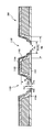
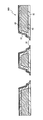
- FIG. 19 is a diagram showing a vapor deposition method using a conventional vapor deposition mask described in Patent Document 1 and Patent Document 2.
- 1901 is a substrate to be processed
- 1902 is a resin layer
- 1903 is a mask body made of a conductor such as a magnetic metal.
- an organic material that is a vapor deposition material is incident from above the mask main body 1903. Actually, the organic material is incident from various directions including an oblique direction.
- FIG. 19B is a diagram showing a film thickness distribution when the opening 1904 provided in the resin layer 1902 is viewed from a direction perpendicular to the surface of the substrate 1901.
- the organic film 1905 is formed with a desired film thickness.
- the edge of the opening is shaded to cause a variation in the film thickness distribution, and a locally thin organic film 1906 is formed.
- the present invention has been made in view of the above-described problems, and an object of the present invention is to provide a vapor deposition mask capable of vapor deposition with a uniform film thickness while increasing the rigidity of the vapor deposition mask as a whole.
- Another object of the present invention is to provide a vapor deposition mask capable of reducing the generation of foreign matters when the vapor deposition mask and the substrate to be processed are in contact with each other.
- a vapor deposition mask includes a main body having a main opening, a side surface of the main opening, an upper surface that intersects the side surface, and a lower surface that intersects the side surface and faces the upper surface. And a first insulator in contact with the lower surface, and a second insulator in contact with the upper surface and the side surface, wherein the first insulator is located inside the main opening. 1 region and a first opening located in the first region, and the second insulator includes a second region located inside the main opening, and the second region.
- the mask body is sandwiched between the first insulator and the second insulator, and one of the first insulator and the second insulator is , Located on the inner side of the main opening than the other, and does not overlap the other and the mask body Has a region.
- a vapor deposition mask includes a mask body having a main opening, a side surface of the main opening, an upper surface intersecting the side surface, and a lower surface intersecting the side surface and facing the upper surface.
- a first insulator in contact with the lower surface, a second insulator in contact with the upper surface and the side surface, and in contact with the second insulator, with the second insulator in contact with the upper surface and the A third insulator facing the side surface, wherein the first insulator includes a first region located inside the main opening, and a first opening located in the first region.
- the second insulator has a second region located inside the main opening, and a second opening located in the second region, and the third insulator is A third region located inside the main opening, and a third opening located in the third region,
- the mask main body is sandwiched between the first insulator and the second insulator, and the third insulator is more in the main opening than the first insulator and the second insulator. It has an area located inside and not overlapping the first insulator, the second insulator, and the mask body.
- a method for manufacturing a vapor deposition mask is a method for manufacturing a vapor deposition mask including a plurality of regularly arranged vapor deposition holes, the step of forming a first insulator on a substrate, Disposing a mask body having a plurality of openings on the first insulator; forming an opening of the first insulator inside the opening of the mask body; and the mask body and the first Forming a second insulator covering one insulator; forming an opening of the second insulator inside the opening of the first insulator; removing the substrate; Is provided.
- a method for manufacturing a vapor deposition mask is a method for manufacturing a vapor deposition mask including a plurality of regularly arranged vapor deposition holes, the step of forming a first insulator on a substrate, Disposing a mask body having a plurality of openings on the first insulator; forming an opening of the first insulator inside the opening of the mask body; and the mask body and the first A step of forming a second insulator covering the one insulator; and the second insulator so as to be disposed inside the opening of the mask body and inside the opening of the first insulator.
- a method for manufacturing a vapor deposition mask is a method for manufacturing a vapor deposition mask including a plurality of regularly arranged vapor deposition holes, the step of forming a first insulator on a substrate, Disposing a mask body having a plurality of openings on the first insulator; forming a second insulator covering the mask body and the first insulator; and inside the openings of the mask body.
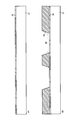
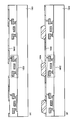
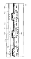
- FIG. 1 shows a schematic configuration of an evaporation mask 100 according to the first embodiment of the present invention.
- FIG. 1A is a plan view of the evaporation mask 100.
- FIG. 1B is an enlarged view in which a frame portion indicated by 101 in FIG.
- the vapor deposition mask 100 of the first embodiment has a structure in which a mask main body made of a conductor is covered with an insulator such as a resin, and includes a plurality of vapor deposition regions 102.
- a metal having a thickness of 30 to 200 ⁇ m made of a magnetic metal such as nickel, a nickel alloy, or Invar can be used as the conductor.
- region 102 is arrange
- the display regions of the plurality of organic EL display devices are collectively configured with an organic material.
- a thin film can be formed.
- the number of vapor deposition regions 102 can be set to an arbitrary number.
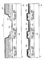
- a plurality of vapor deposition holes 103 are formed in each vapor deposition region 102.
- a slit is formed as the vapor deposition hole 103 is shown, but for example, an opening having an arbitrary shape such as a circle or a rectangle is provided in addition to the slit depending on the pixel arrangement of the organic EL display device. It may be provided.
- alignment marks 104 are provided at the four corners of the evaporation mask 100. This is a mask-side marker used for alignment between the evaporation target substrate and the evaporation mask 100. These may be provided near the center of each side.
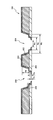
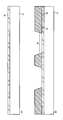
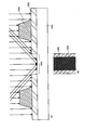
- FIG. 1B a cross-sectional view of the vapor deposition region 102 cut along X-X ′ is shown in FIG.
- FIG. 2 A perspective view centering on the slit portion is shown in FIG. In FIG. 2, it appears to be separated into three parts, but in reality, all are physically connected as shown in FIG.
- 201 is a first insulator
- 202 is a mask body (for example, a mask material made of a conductor)
- 203 is a second insulator.
- the mask main body 202 is a portion that is a basic skeleton of the vapor deposition mask 100 shown in FIG. 1 and is typically made of a magnetic metal such as nickel, a nickel alloy, or invar.
- a metal foil (metal sheet) having an invar characteristic that has a small thermal expansion coefficient and is not easily affected by heat is used as the mask body 202.
- the cross section of the mask body 202 is trapezoidal. This is because the inner wall of the vapor deposition hole 204 (corresponding to the vapor deposition hole 103 in FIG. 1) in the vapor deposition mask 100 is tapered.
- the shape of the mask main body 202 is not limited to a trapezoid, and may be a shape in which the side surface of the trapezoidal portion constituting the mask main body in FIG. In other words, the shape is not particularly limited as long as the side surface of the mask body 202 has an inclination.
- the first insulator 201 and the second insulator 203 an organic film made of a resin such as polyimide, epoxy, acrylic, or polyethylene terephthalate (PET) can be used.
- An inorganic film such as silicon nitride or silicon oxide may be used.
- the first insulator 201 and the second insulator 203 can be formed of the same kind of organic film, the first insulator 201 can be an organic film, and the second insulator 203 can be an inorganic film.
- a feature of the evaporation mask 100 of this embodiment is that a mask body 202 made of magnetic metal is covered with two insulators, a first insulator 201 and a second insulator 203. Thereby, it is possible to realize a vapor deposition mask having fine vapor deposition holes (slit shape or rectangular holes) while maintaining the overall strength (rigidity).
- the inner wall of the vapor deposition hole of the vapor deposition mask 100 is stepped and has a substantially tapered shape, there is almost no shadow on the vapor deposition material incident from various angles, and the film thickness distribution is uniform. A vapor-deposited film can be formed.
- the mask body 202 does not directly contact the deposition target substrate. Therefore, there is no generation of foreign matter (for example, metallic foreign matter) due to contact between the two, high yield, and highly reliable vapor deposition is possible.
- foreign matter for example, metallic foreign matter
- the thickness of the first insulator 201 is Ha (typically 5 to 20 ⁇ m)
- the thickness of the mask body 202 is Hb (typically 10 to 50 ⁇ m)
- the film of the second insulator 203 is formed.
- Hc typically 1 to 5 ⁇ m
- Hc ⁇ Ha there is a relationship Hc ⁇ Ha between the film thickness (Ha) of the first insulator 201 and the film thickness (Hc) of the second insulator 203. It is desirable that the relationship holds.
- the film thickness (Ha) of the first insulator 201 is 10 ⁇ m
- the thickness (Hb) of the mask body 202 is 30 ⁇ m
- the film thickness (Hc) of the second insulator 203 is 5 ⁇ m. It is said.
- the inner wall of the vapor deposition hole 204 is covered with the second insulator 203, and only the second insulator 203 is provided on the bottom thereof with a film thickness (Hc) of about 1 to 5 ⁇ m. Therefore, as shown in FIG. 19A, a shadow is not formed on the evaporation material (typically an organic material) at the end of the opening. Accordingly, variation in the film thickness distribution of the deposited film as described with reference to FIG. 19B can be prevented.
- Hc film thickness
- the film thickness (Ha) of the first insulator 201 is 10 to 20 ⁇ m, the rigidity of the mask body 202 is reinforced, and the overall rigidity of the vapor deposition mask 100 can be increased. Even in this case, by setting the film thickness (Hc) of the second insulator 203 to 3 to 5 ⁇ m, no shadow is formed on the vapor deposition material at the bottom of the vapor deposition pattern hole. Distribution variation can be prevented.
- the width of the first opening (slit) formed in the first insulator 201 is Wa (typically 25 to 45 ⁇ m), and the width of the main opening formed in the mask body 202 is Wb (typically 30 to 50 ⁇ m), and the width of the second opening formed in the second insulator 203 is Wc (typically 20 to 40 ⁇ m). It is desirable that the relationship of Wc ⁇ Wa ⁇ Wb is satisfied.
- the width (Wa) of the first opening formed in the first insulator 201 is 35 ⁇ m
- the width (Wb) of the main opening formed in the mask body 202 is 40 ⁇ m
- the width (Wc) of the second opening formed in the second insulator 203 is 30 ⁇ m.
- the pitch of the vapor deposition holes 204 is 60 ⁇ m, but is not limited to this value.
- the width (Wc) of the second opening formed in the second insulator 203 corresponds to the width (slit width) of the vapor deposition hole 103 shown in FIG. That is, in the vapor deposition mask 100 of this embodiment, the width (Wc) of the second opening formed in the second insulator 203 substantially determines the opening width of the vapor deposition hole 204 in the vapor deposition mask 100. To do.
- the first opening of the first insulator 201 is positioned inside the main opening formed in the mask body 202, and further, 2nd opening part of 2 insulator 203 is located.
- a stepped (substantially tapered) step is formed on the inner wall of the vapor deposition hole 204, and the vapor deposition material incident from various angles is more easily incident.
- the evaporation mask 100 shown in FIG. 2 has a main opening, a side surface of the main opening, an upper surface that intersects the side surface, and a lower surface that intersects the side surface and faces the upper surface. 202. Furthermore, a first insulator 201 in contact with the lower surface and a second insulator 203 in contact with the upper surface and the side surface are provided.
- the first insulator 201 has a first region located inside the main opening, and a first opening located in the first region.
- the second insulator 203 has a second region located inside the main opening, and a second opening located in the second region.
- the mask body 202 is sandwiched between the first insulator 201 and the second insulator 203.
- One of the first insulator 201 and the second insulator 203 (second insulator 203 in FIG. 2) is positioned on the inner side of the main opening than the other (first insulator 201 in FIG. 2). And a region that does not overlap the other and the mask body 202.
- the film thickness of the second insulator 203 is thinner than the film thickness of the first insulator 201.
- the second insulator 203 is positioned inside the main opening rather than the first insulator 201.
- the second opening included in the second insulator 203 is located on the inner side than the first opening included in the first insulator 201.
- the second region located at the end of the second opening has a structure that does not overlap the first insulator 201 and the mask body 202.
- the evaporation mask 100 shown in FIG. 2 has a portion in which the first region does not overlap the second insulator 203 and the mask body 202, and the main region is formed by the portion and the second region. A step is formed inside the opening.
- the first insulator 201 located under the mask body 202 has a predetermined film thickness and can maintain the strength of the evaporation mask 100.
- the second insulator 203 thinner than the first insulator 201 is located on the innermost side of the vapor deposition hole 204 provided in the vapor deposition mask 100. That is, the thickness of the end portion of the vapor deposition hole 204 can be reduced. Thereby, it can reduce that the entrance of a vapor deposition material is prevented by the edge part of the vapor deposition hole 204.
- FIG. Accordingly, variation in film thickness distribution shown in FIGS. 19A and 19B can be suppressed. This effect becomes more prominent as the vapor deposition hole 204 becomes smaller due to higher definition. Therefore, the configuration of the present embodiment has an effect that the thickness of the deposited film can be made uniform without reducing the strength of the deposition mask.
- the first opening of the first insulator 201 is located inside the main opening formed in the mask body 202, the first insulator 201 and the second insulator 203 are: As shown by the frame line 205, the surfaces touch each other. Thus, the mask body 202 is sandwiched between the first insulator 201 and the second insulator 203, and the mask body 202 can be completely covered. Therefore, even if the substrate to be deposited and the deposition mask 100 are brought into contact with each other, the generation of foreign matters due to the contact between them can be prevented.
- the second insulator 203 is in contact with the first insulator 201 on the surface, occurrence of defects due to film peeling of the first insulator 201 is reduced, and durability of the evaporation mask can be improved.
- ⁇ Method for manufacturing vapor deposition mask> 4 to 6 show a method of manufacturing the vapor deposition mask 100 according to the first embodiment of the present invention.
- a resin film made of polyimide is formed on the support substrate 11 as the first insulator 12.
- the first insulator 12 can be formed by applying polyimide using a known spin coating method or printing method and then curing the polyimide by light irradiation or heating.
- the film thickness (Ha) of the first insulator 12 is 10 ⁇ m.
- an adhesive sheet may be separately provided between the support substrate 11 and the first insulator 12 in order to finally peel off the first insulator 12 from the support substrate 11.
- an adhesive sheet having such a property that the adhesive force can be weakened by light irradiation or heating, such as a known dicing tape.
- a glass substrate is used as the support substrate 11.
- the support substrate 11 is used for the purpose of supporting various thin films and the mask body in the manufacturing process of the evaporation mask, and is finally removed when the evaporation mask 100 is completed on the support substrate 11.
- the material is not particularly limited, and any substrate can be used as long as it can support the resin film and the mask body (mask pattern) during the manufacturing process, such as a metal substrate, a ceramic substrate, and a plastic substrate.
- the first insulator 12 not only polyimide but also an organic film (thin film made of an organic material) made of a resin such as epoxy, acrylic, or polyethylene terephthalate can be used.
- an inorganic film a thin film made of an inorganic material
- silicon oxide or silicon nitride may be used.
- a mask main body (a conductor sheet provided with an opening for vapor deposition) 13 which is a basic skeleton of the vapor deposition mask is bonded.
- a metal foil (metal sheet) using an invar material that is a magnetic metal is used as the mask body 13 .
- the thickness (Hb) of the mask body 13 is 30 ⁇ m.
- a mask main body 13 provided with a plurality of openings (slits) 14 in advance is prepared (the plan view is the same as that in FIG. 1A), and the mask main body 13 is first bonded using an adhesive. Adhere to the insulator 12.
- the 1st insulator 12 function as an adhesive agent by bonding the mask main body 13 before hardening the 1st insulator 12, and hardening the 1st insulator 12 after that.
- the width (Wb) of the main opening 14 provided in the mask main body 13 is 40 ⁇ m as described above.
- the mask body 13 prepared in advance is shown as an example.
- a conductive film made of magnetic metal is formed on the first insulator 12, and the conductive film is patterned to form a mask.
- nickel is used as the magnetic metal, and a nickel thin film is formed on the first insulator 12 by a known plating method. Thereafter, the nickel thin film can be patterned by known photolithography to form a mask body.
- the formation of the nickel thin film is not limited to the plating method, and may be formed using a CVD method or a sputtering method.
- the first insulator 12 is etched to form a plurality of openings 15.
- the plurality of openings 15 are formed in a stripe shape in the vapor deposition region 102, and thus the first insulator 12 is also formed in a stripe shape in the vapor deposition region 102.
- the shape of the opening 15 is not limited to the stripe shape, and an appropriate shape may be selected according to the pattern arrangement of the vapor deposition material.
- the opening 15 is formed using laser etching. Since the film thickness of the first insulator 12 is 5 to 20 ⁇ m (10 ⁇ m in this embodiment), anisotropic etching in which etching proceeds selectively in the vertical direction is desirable. In this embodiment, an example in which laser etching is used has been described. However, anisotropic etching may be performed by dry etching using an etching gas.
- the width (Wa) of the opening 15 provided in the first insulator 12 is 35 ⁇ m as described above.
- the first insulator 12 is etched in FIG. 5A after the mask body 13 is formed in FIG. 4B.
- the mask body 13 can be bonded or formed after the order is reversed and the first insulator 12 is etched to form the opening 15.
- the second insulator 16 is formed so as to cover the mask body 13 and the first insulator 12.
- the second insulator 16 can be formed by applying polyimide using a known spin coating method or printing method and then curing the polyimide by light irradiation or heating.
- the film thickness (Hc) of the second insulator 16 is 5 ⁇ m.
- the second insulator 16 it is possible to use not only polyimide but also an organic film (thin film made of an organic material) made of a resin such as epoxy, acrylic or polyethylene terephthalate.
- an inorganic film a thin film made of an inorganic material
- silicon oxide or silicon nitride may be used.
- polyimide having low viscosity when applying polyimide as the second insulator 16.
- the planarization effect can be given to the 2nd insulator 16, and the vapor deposition hole of the final vapor deposition mask 100 can be made into a smoother taper shape.
- the second insulator 16 is processed by laser etching to form a plurality of openings 17.
- the plurality of openings 17 are formed in a stripe shape in the vapor deposition region 102
- the second insulator 16 is also formed in a stripe shape in the vapor deposition region 102.
- the opening 17 is formed so that the mask body 13 and the first insulator 12 are completely covered by the second insulator 16. That is, the opening 17 of the second insulator 16 is formed inside the opening 15 of the first insulator 12 formed in FIG. As described above, the width (Wc) of the opening 17 provided in the second insulator 16 is 30 ⁇ m.
- anisotropic etching is performed by dry etching using an etching gas, as in the case of etching the first insulator 12. It is also possible.
- FIG. 6B the support substrate 11 is peeled off. Thereby, the vapor deposition mask 100 of the present embodiment having the structure and effect described with reference to FIGS. 1 to 3 is completed.
- the structure is such that the mask body (conductor sheet) 13 that is the basic skeleton of the vapor deposition mask is sandwiched between the first insulator 12 and the second insulator 16. .
- the vapor deposition mask 100 having fine vapor deposition holes (slits or rectangular holes) can be realized while maintaining the strength (rigidity) of the entire vapor deposition mask.
- the inner wall of the vapor deposition hole 103 of the final vapor deposition mask 100 has a stepped shape (substantially tapered shape), there is almost no shadow on the vapor deposition material incident from various angles. Therefore, the vapor deposition mask 100 capable of forming a vapor deposition film having a uniform film thickness distribution can be manufactured.
- the mask body 13 can be deposited even when the deposition target substrate and the deposition mask 100 are brought into contact with each other. There is no direct contact with the substrate. Therefore, it is possible to manufacture a highly reliable vapor deposition mask that does not generate foreign matter (for example, metallic foreign matter) due to contact between the two.
- the etching is performed in a state where the mask body 13 and the first insulator 12 are covered with the second insulator 16, so that the film of the first insulator 12 is peeled off, and the mask body It is possible to reduce problems such as thermal expansion 13 and generation of foreign matter from the mask main body 13.
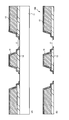
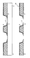
- FIG. 7 shows a cross-sectional structure of a vapor deposition mask 200 according to the second embodiment of the present invention.
- the vapor deposition mask 200 of the second embodiment has a schematic configuration as shown in FIG. 1, but the cross-sectional structure is different from that of the vapor deposition mask 100 of the first embodiment.
- the first opening formed in the first insulator is located inside the second opening formed in the second insulator. This is different from the vapor deposition mask 100 of the first embodiment.
- Other points are the same as those of the vapor deposition mask 100 of the first embodiment.
- 701 is a first insulator
- 702 is a mask body
- 703 is a second insulator.
- a metal foil made of an invar material is used as the mask body 702
- polyimide is used as the first insulator 701 and the second insulator 703.
- the materials constituting the first insulator 701, the mask body 702, and the second insulator 703 are not limited to those described in the first embodiment.
- the thickness of the first insulator 701 is Ha (typically 1 to 5 ⁇ m)
- the thickness of the mask body 702 is Hb (typically 10 to 50 ⁇ m)
- the film of the second insulator 703 is formed.
- Hc typically 10 to 20 ⁇ m
- Ha ⁇ Hc there is a relationship Ha ⁇ Hc between the film thickness (Ha) of the first insulator 701 and the film thickness (Hc) of the second insulator 703. It is desirable that the relationship holds.
- the film thickness (Ha) of the first insulator 701 is 5 ⁇ m
- the thickness (Hb) of the mask body 702 is 30 ⁇ m
- the film thickness (Hc) of the second insulator 703 is 10 ⁇ m. It is said.
- the first insulator 701 having a film thickness Ha is provided in the vicinity of the hole through which the vapor deposition material passes at the bottom of the vapor deposition hole 704. Therefore, as shown in FIG. 19A, a shadow is not formed on the evaporation material (typically an organic material) at the end of the opening. Accordingly, variation in the film thickness distribution of the deposited film as described with reference to FIG. 19B can be prevented.
- the film thickness (Hc) of the second insulator 703 is set to 10 to 20 ⁇ m, the rigidity of the mask body 702 can be reinforced, and the overall rigidity of the evaporation mask 200 can be increased. Even in this case, the film thickness (Ha) of the first insulator 701 is set to 3 to 5 ⁇ m so that no shadow is formed on the vapor deposition material at the end of the opening. Distribution variation can be prevented.
- the width of the first opening formed in the first insulator 701 is Wa (typically 20 to 40 ⁇ m), and the width of the main opening formed in the mask body 702 is Wb (typically 30 to 50 ⁇ m), and the width of the second opening formed in the second insulator 703 is Wc (typically 25 to 45 ⁇ m), It is desirable that the relationship of Wa ⁇ Wc ⁇ Wb holds.
- the width (Wa) of the first opening formed in the first insulator 701 is 30 ⁇ m
- the width (Wb) of the main opening formed in the mask body 702 is 40 ⁇ m.
- the width (Wc) of the second opening formed in the second insulator 703 is set to 35 ⁇ m.
- the width (Wa) of the first opening formed in the first insulator 701 corresponds to the width (slit width) of the vapor deposition hole 103 shown in FIG. That is, in the vapor deposition mask 200 of this embodiment, the width (Wa) of the first opening formed in the first insulator 701 substantially determines the opening width of the vapor deposition hole 704 in the vapor deposition mask 200. To do.
- the second opening of the second insulator 703 is positioned inside the main opening formed in the mask body 702, and the second opening is further inside.
- a first opening of one insulator 701 is located. That is, a stepped (substantially tapered) step is formed on the inner wall of the vapor deposition hole 704, and the vapor deposition material incident from various angles is more easily incident.
- the first insulator 701 is positioned more inside than the second opening 703 than the second opening 703, and the second opening included in the second insulator 703.
- the 1st opening which the 1st insulator 701 has is located inside rather than.
- a region of the first insulator 701 located at the end of the first opening has a structure that does not overlap the second insulator 703 and the mask body 702.
- the film thickness of the first insulator 701 is thinner than the film thickness of the second insulator 703.
- the first insulator 701 has a portion that does not overlap the second insulator 703 and the mask body 702, and a step is formed inside the main opening between the portion and the second insulator 703. Yes.
- the first insulator 701 and the second insulator 703 are in contact with each other as indicated by a frame line 705. Thereby, the mask main body 702 can be completely covered with the first insulator 701 and the second insulator 703. For this reason, even if the substrate to be deposited and the deposition mask 200 are brought into contact with each other, it is possible to prevent the generation of foreign matters due to the contact between them.
- ⁇ Method for manufacturing vapor deposition mask> 8 to 10 show a method for manufacturing the evaporation mask 200 according to the second embodiment of the present invention.
- the vapor deposition mask 200 of the second embodiment uses an insulator or a conductor made of the same material as the vapor deposition mask 100 of the first embodiment except that the cross-sectional structure and the film thickness of the insulating film are different. Is possible. Therefore, although not redundantly described in this embodiment, each element such as an insulator and a conductor is not limited to the example shown in this embodiment, and the materials described in the first embodiment can be used. .
- a resin film made of polyimide is formed as the first insulator 22 on the support substrate 21 made of a glass substrate.
- the first insulator 12 can be formed by applying polyimide using a known spin coating method or printing method and then curing the polyimide by light irradiation or heating.
- the film thickness (Ha) of the first insulator 12 is 5 ⁇ m.
- an adhesive sheet (not shown) may be separately provided between the support substrate 21 and the first insulator 22 in this embodiment.
- a mask body (conductor sheet) 23 serving as a basic skeleton of the evaporation mask is bonded onto the first insulator 22.
- a metal foil (metal sheet) using an invar material that is a magnetic metal is used as the mask body.
- the mask body 23 has a thickness (Hb) of 30 ⁇ m.
- the 1st insulator 22 function as an adhesive agent by bonding the mask main body 23 before hardening the 1st insulator 22, and hardening the 1st insulator 22 after that.
- the width (Wb) of the main opening 24 provided in the mask main body 23 is 40 ⁇ m as described above.
- the first insulator 22 is etched to form a plurality of openings 25.
- the opening 25 is formed using laser etching.
- anisotropic etching by dry etching using an etching gas may be used instead of laser etching.
- the width (Wa) of the opening 25 provided in the first insulator 22 is 30 ⁇ m as described above.
- the first insulator 22 is etched after the mask body 23 is formed, but the mask body 23 is bonded or formed after the first insulator 22 is etched to form the opening 25. It is also possible to do.
- a polyimide film is formed as the second insulator 26 so as to cover the mask body 23 and the first insulator 22.
- the second insulator 26 can be formed by applying polyimide using a known spin coating method or printing method and then curing the polyimide by light irradiation or heating.
- the film thickness (Hc) of the second insulator 26 is 10 ⁇ m.
- polyimide having low viscosity when applying polyimide as the second insulator 26.
- the planarization effect can be given to the 2nd insulator 26, and the opening part of the final vapor deposition mask can be made into a smoother taper shape.
- the second insulator 26 is processed by laser etching to form a plurality of openings 27.
- the plurality of openings 27 are formed in a stripe shape in the vapor deposition region, the second insulator 26 is also formed in a stripe shape in the vapor deposition region.
- the opening 27 is formed so that the mask body 23 is completely covered by the second insulator 26. Specifically, the opening 27 is formed wider than the opening 25 formed in FIG. 9A, and the mask main body 23 is sandwiched between the first insulator 22 and the second insulator 26.
- the width (Wc) of the opening 27 provided in the second insulator 26 is 35 ⁇ m as described above.
- the opening 27 is formed using laser etching.
- anisotropic etching using an etching gas may be used as in the etching of the first insulator 22. It is.
- the time control is strictly performed when the second insulator 26 is etched. Thereby, after the etching of the second insulator 26 is completed, the amount by which the first insulator 22 is etched can be minimized.
- a mask body (conductor sheet) 23 that is a basic skeleton of the evaporation mask is sandwiched between the first insulator 22 and the second insulator 26. .
- a vapor deposition mask having fine vapor deposition holes (slits or rectangular holes) while maintaining the strength (rigidity) of the entire vapor deposition mask.
- the inner wall of the vapor deposition hole 704 of the final vapor deposition mask 200 has a stepped shape (substantially tapered shape), there is almost no shadow on the vapor deposition material incident from various angles. Therefore, the vapor deposition mask 200 capable of forming a vapor deposition film having a uniform film thickness distribution can be manufactured.
- the mask body 23 can be deposited even when the deposition target substrate and the deposition mask 200 are brought into contact with each other. There is no direct contact with the substrate. Therefore, it is possible to manufacture a highly reliable vapor deposition mask that does not generate foreign matter (for example, metallic foreign matter) due to contact between the two.
- the etching is performed in a state where the mask body 23 is covered with the second insulator 26, so that problems such as thermal expansion of the mask body 23 and generation of foreign matter from the mask body 23 are reduced. can do.
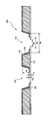
- FIG. 11 shows a cross-sectional structure of an evaporation mask 300 according to the third embodiment of the present invention.
- the vapor deposition mask 300 of the third embodiment has a schematic configuration as shown in FIG. 1, but the cross-sectional structure is different from that of the vapor deposition mask 100 of the first embodiment.
- the vapor deposition mask 300 of the third embodiment is different from the vapor deposition mask 100 of the first embodiment in that the mask body is sandwiched between two insulators and then covered with another insulator. Other points are the same as those of the vapor deposition mask of the first embodiment.
- 1101 is a first insulator
- 1102 is a mask body
- 1103 is a second insulator
- 1104 is a third insulator.
- a metal foil made of an invar material is used as the mask body 1102
- polyimide is used as the first insulator 1101, the second insulator 1103, and the third insulator 1104.
- the materials constituting the first insulator 1101, the mask body 1102, the second insulator 1103, and the third insulator 1104 are not limited to those described in the first embodiment.
- the first insulator 1101, the second insulator 1103, and the third insulator 1104 are not only polyimide but also organic films (thin films made of organic materials) made of resin such as epoxy, acrylic, and polyethylene terephthalate. It is possible to use. Alternatively, an inorganic film (a thin film made of an inorganic material) such as silicon oxide or silicon nitride may be used. Furthermore, these organic films and inorganic films may be arbitrarily combined.
- the film thickness of the first insulator 1101 is Ha (typically 1 to 20 ⁇ m)
- the thickness of the mask body 1102 is Hb (typically 30 to 200 ⁇ m)
- the film thickness (Ha) of the first insulator 1101 is It is desirable that a relationship of Hd ⁇ Ha or Hd ⁇ Hc is established between the film thickness (Hc) of the second insulator 1103 and the film thickness (Hd) of the third insulator 1104.
- the film thickness (Ha) of the first insulator 1101 is 10 ⁇ m
- the thickness (Hb) of the mask body 1102 is 30 ⁇ m
- the film thickness (Hc) of the second insulator 1103 is 10 ⁇ m
- the film thickness (Hd) of the third insulator 1104 is 5 ⁇ m.
- the inner wall of the vapor deposition hole 1105 is covered with the third insulator 1104, and only the third insulator 1104 is provided at the bottom thereof with a film thickness (Hd) of about 3 to 5 ⁇ m. Therefore, as shown in FIG. 19A, a shadow is not formed on the evaporation material (typically an organic material) at the end of the opening. Accordingly, variation in the film thickness distribution of the deposited film as described with reference to FIG. 19B can be prevented.
- Hd film thickness
- the rigidity of the mask body 1102 is reinforced, and the entire deposition mask 300 is formed. Rigidity can be increased. Even in this case, since the thickness (Hd) of the third insulator 1104 is set to 3 to 5 ⁇ m, no shadow is formed on the vapor deposition material at the end of the opening. Distribution variation can be prevented.
- first insulator 1101, the second insulator 1103, and the third insulator 1104 can all be inorganic insulators of about 1 ⁇ m, and a tapered shape that also serves as reinforcement of the opening can be formed.
- the width of the first opening formed in the first insulator 1101 is Wa (typically 25 to 45 ⁇ m)
- the width of the main opening formed in the mask body 1102 is Wb (typically 30 to 50 ⁇ m)
- the width of the second opening formed in the second insulator 1103 is Wc (typically 25 to 45 ⁇ m)
- the width of the third opening formed in the third insulator 1104 is
- Wd typically 20 to 40 ⁇ m
- the first insulator 1101 and the second insulator 1103 are collectively etched to form an opening, so that the film thickness (Ha) of the first insulator 1101 and the second insulator 1103
- the film thickness (Hc) is almost equal.
- “substantially equal” includes not only the case where they completely match, but also the case where there is a slight difference.
- Wa? Wc In the description about the width of the opening described above, it is expressed as Wa? Wc based on this point. That is, since both the first insulator 1101 and the second insulator 1103 have a film thickness of 10 to 20 ⁇ m, there is a slight difference in the opening width between the two when etched so as to have a tapered cross section. Means.
- the width (Wa) of the first opening formed in the first insulator 1101 is 35 ⁇ m
- the width (Wb) of the main opening formed in the mask body 1102 is 40 ⁇ m
- the width (Wc) of the second opening formed in the second insulator 1103 is 35 ⁇ m
- the width (Wd) of the third opening formed in the third insulator 1104 is 30 ⁇ m.
- the width (Wd) of the third opening formed in the third insulator 1104 corresponds to the width (slit width) of the vapor deposition hole 103 shown in FIG. That is, in the vapor deposition mask 300 of this embodiment, the width (Wd) of the third opening formed in the third insulator 1104 substantially determines the opening width of the vapor deposition hole 1105 in the vapor deposition mask 300. To do.
- the openings of the first insulator 1101 and the second insulator 1103 are located inside the main opening formed in the mask body 1102, and further, The third opening of the third insulator 1104 is located inside.
- a stepped (substantially tapered) step is formed on the inner wall of the vapor deposition hole 1105, and the vapor deposition material incident from various angles is more easily incident.
- the evaporation mask 300 shown in FIG. 11 has a main opening, a side surface of the main opening, an upper surface intersecting the side surface, and a lower surface intersecting the side surface and facing the upper surface.
- a main body 1102 is provided. Further, the first insulator 1101 in contact with the lower surface, the second insulator 1103 in contact with the upper surface and the side surface, and the second insulator 1103 in contact with the second insulator 1103.
- the first insulator 1101 has a first region located inside the main opening, and a first opening located in the first region.
- the second insulator 1103 has a second region located inside the main opening, and a second opening located in the second region.
- the third insulator 1104 has a third region located inside the main opening, and a third opening located in the third region.
- the mask body 1102 is sandwiched between the first insulator 1101 and the second insulator 1103.
- the third insulator 1104 is located on the inner side of the main opening than the first insulator 1101 and the second insulator 1103, and is connected to the first insulator 1101, the second insulator 1103, and the mask body 1102. Has non-overlapping areas.
- the evaporation mask 300 illustrated in FIG. 11 includes the film thickness of the third insulator among the film thickness of the first insulator 1101, the second insulator 1103, the film thickness, and the film thickness of the third insulator 1104.
- 1104 is the thinnest.
- the third opening is located on the innermost side among the first opening, the second opening, and the third opening.
- the third region is formed on a portion that does not overlap the first insulator 1101, the second insulator 1103, and the mask main body 1102, the side surface of the first opening, and the side surface of the second opening.
- a step is formed on the inner side of the main opening between the portion in contact with the portion and the portion in contact with the upper surface of the second region.
- the first insulator 1101 and the second insulator 1103 are in contact with each other as indicated by a frame line 1106. Thereby, the mask main body 1102 can be completely covered with the first insulator 1101 and the second insulator 1103. Therefore, even if the substrate to be deposited and the deposition mask 300 are brought into contact with each other, it is possible to prevent the generation of foreign matters due to the contact between them.
- ⁇ Method for manufacturing vapor deposition mask> 12 to 15 show a method of manufacturing the evaporation mask 300 according to the third embodiment of the present invention.
- the vapor deposition mask 300 of the third embodiment uses an insulator or a conductor made of the same material as the vapor deposition mask 100 of the first embodiment except that the cross-sectional structure and the film thickness of the insulating film are different. Is possible. Therefore, although not redundantly described in this embodiment, each element such as an insulator and a conductor is not limited to the example shown in this embodiment, and the materials described in the first embodiment can be used. .
- a resin film made of polyimide is formed as a first insulator 32 on a support substrate 31 made of a glass substrate.
- the first insulator 32 can be formed by applying polyimide using a known spin coating method or printing method and then curing the polyimide by light irradiation or heating.
- the film thickness (Ha) of the first insulator 32 is 10 ⁇ m.
- an adhesive sheet (not shown) may be separately provided between the support substrate 31 and the first insulator 32 in this embodiment.
- a mask main body (conductor sheet) 33 which is a basic skeleton of the evaporation mask is bonded onto the first insulator 32.
- a metal foil (metal sheet) using an invar material that is a magnetic metal is used as the mask body.
- the thickness (Hb) of the mask main body 33 is 30 ⁇ m.
- the 1st insulator 32 function as an adhesive agent by bonding the mask main body 33 before hardening the 1st insulator 32, and hardening the 1st insulator 32 after that.
- the width (Wb) of the main opening 34 provided in the mask main body 33 is 40 ⁇ m as described above.
- a mask body 33 prepared in advance is adhered is shown.
- a mask body is formed by patterning. May be.
- a second insulator 35 made of polyimide is formed so as to cover the mask body 33.
- the second insulator 35 can be formed by applying polyimide using a known spin coating method or printing method and then curing the polyimide by light irradiation or heating.
- the film thickness (Hc) of the second insulator 35 is 10 ⁇ m.
- the first insulator 32 and the second insulator 35 are collectively etched to form a plurality of openings 36.
- the opening 36 is formed using laser etching.
- anisotropic etching by dry etching using an etching gas may be used instead of laser etching.
- the width (Wa, Wc) of the opening 36 provided in each of the first insulator 32 and the second insulator 35 is 30 ⁇ m as described above.
- a polyimide film is formed as a third insulator 37 so as to cover the first insulator 32, the mask body 33, and the second insulator 35.
- the third insulator 37 can be formed by applying polyimide using a known spin coating method or printing method and then curing the polyimide by light irradiation or heating.
- the film thickness (Hd) of the third insulator 37 is 5 ⁇ m.
- polyimide having low viscosity when applying polyimide as the third insulator 37.
- the planarization effect can be given to the 3rd insulator 37, and the vapor deposition hole of the final vapor deposition mask can be made into a smoother taper shape.
- the third insulator 37 is processed by laser etching to form a plurality of openings 38.
- the third insulator 37 is also formed in a stripe shape in the vapor deposition region.
- the opening 38 is formed so that the first insulator 32 and the second insulator 35 are completely covered by the third insulator 37. Specifically, the opening 38 is formed inside the opening 36 formed in FIG.
- the width (Wd) of the opening 38 provided in the third insulator 37 is 30 ⁇ m as described above.
- the opening 38 is formed using laser etching.
- anisotropy using an etching gas is used. It is also possible to use etching.
- the structure is such that the mask body (conductor sheet) 33 that is the basic skeleton of the vapor deposition mask is sandwiched between the first insulator 32 and the second insulator 35. .
- the inner wall of the vapor deposition hole 1105 of the final vapor deposition mask 300 has a stepped shape (substantially tapered shape), there is almost no shadow on the vapor deposition material incident from various angles. Therefore, the vapor deposition mask 300 capable of forming a vapor deposition film having a uniform film thickness distribution can be manufactured.
- the mask body 33 can be deposited even when the deposition target substrate and the deposition mask 300 are in contact with each other. There is no direct contact with the substrate. Therefore, it is possible to manufacture a highly reliable vapor deposition mask that does not generate foreign matter (for example, metallic foreign matter) due to contact between the two.
- the etching is performed in a state where the mask body 33 is covered with the first insulator 32 and the second insulator 35. Problems such as the generation of foreign matter can be reduced.
- FIG. 16 is a diagram showing a method for manufacturing the organic EL display device according to this embodiment.
- a thin film transistor (TFT) 1602 is formed over a substrate 1601 by a known method. Since the organic EL display device of this embodiment has a top emission structure that emits light vertically upward (direction toward the counter substrate) with respect to the pixel electrode 1603, a glass substrate, a ceramic substrate, or a plastic substrate is used as the substrate 1601. Any of the metal substrates may be used.
- the thin film transistor 1602 may have a top gate structure or a bottom gate structure.
- the thin film transistor 1602 functions as a switching element in the pixel region, and the structure and conductivity type (n-type or P-type) may be determined as appropriate.
- the pixel electrode 1603 formed by a known method is connected to the thin film transistor 1602.
- a metal film having a high reflectance is preferably used as the pixel electrode 1603 in order to obtain a top emission structure as described above.
- ITO Indium Tin Oxide
- the pixel electrode 1603 functions as an anode of the organic EL element.
- a bank 1604 is formed in each gap between the plurality of pixel electrodes 1603.
- the bank 1604 may be formed using a resin film such as polyimide or acrylic.
- a resin film such as polyimide or acrylic.
- an inorganic material such as silicon nitride or silicon oxide may be used, or a resin material and an inorganic material may be laminated and used.
- a light emitting layer 1606 constituting an EL element is formed by a vapor deposition method using a vapor deposition mask 1605 as shown in FIG.
- formation of the light emitting layer 1606 corresponding to any of RGB is illustrated.
- the vapor deposition mask 1605 is exemplified by the structure described in the first embodiment described above, but any one of the vapor deposition masks in the first to third embodiments may be used.
- the vapor deposition mask 1605 is fixed in a state where tension is applied to a frame made of nickel alloy or stainless steel.
- the evaporation mask 1605 is attracted by a magnetic force from the back surface side (the surface side where no element is formed) of the substrate 1601 and is used in close contact with the formation surface of the EL element.
- the vapor deposition mask 1605 is provided with vapor deposition holes 1607 having a width corresponding to each pixel.
- the organic material constituting the light emitting layer 1606 passes through the vapor deposition hole 1607 of the vapor deposition mask 1605 and is deposited on the surface of the pixel electrode 1603 to form the light emitting layer 1606.
- a red light emitting layer that emits red light, a green light emitting layer that emits green light, and a blue light emitting layer that emits blue light are formed as separate vapor deposition steps while sequentially shifting the vapor deposition mask 1605.
- a dot-like or slot-like structure opened in each pixel unit may be adapted to the shape of the pixel.
- a common electrode 1609 functioning as a cathode of the EL element and a protective film 1610 are formed.
- the common electrode 1609 is preferably formed of a transparent conductive film such as light-transmitting ITO or IZO (zinc oxide doped with indium).
- an insulating film eg, a silicon nitride film
- a multilayer structure in which an organic film such as an acrylic resin is sandwiched between lower layers or intermediate layers may be used as a stress relaxation structure or a foreign matter countermeasure structure.
- An active matrix substrate refers to a substrate on which a switching element including a thin film transistor and a light emitting element such as an organic EL element are formed.
- reference numeral 1611 denotes a glass substrate. If necessary, a red color filter 1612a corresponding to a red pixel, a green color filter 1612b corresponding to a green pixel, and a blue color filter 1612c corresponding to a blue pixel may be used.
- Reference numeral 1613 denotes a black mask provided between the color filters. These color filters 1612a to 1612c and the black mask 1613 may be formed by a known method.
- the counter substrate in the organic EL display device of this embodiment includes the glass substrate 1611, the red color filter 1612a, the green color filter 1612b, the blue color filter 1612c, and the black mask 1613.
- the color filters 1612a to 1612c and the black mask 1613 are not essential components, and may be omitted.
- the active matrix substrate shown in FIG. 17B and the above-described counter substrate are bonded using a filling layer 1614 made of a resin to complete the organic EL display device shown in FIG.
- a filling layer 1614 made of a resin to complete the organic EL display device shown in FIG.
- a transparent resin such as polyimide or acrylic can be used.
- curing may be performed by light irradiation.
- a light emitting layer having a uniform film thickness distribution can be formed by forming a light emitting layer using the vapor deposition mask 1605 of the present invention.
- the mask body constituting the evaporation mask 1605 does not directly touch the pixel electrode 1603 or the bank 1604, so that the yield of the manufacturing process is improved.
- Evaporation mask 102 Evaporation area
- region 103 Evaporation hole 104: Alignment mark 201: 1st insulator 202: Mask main body 203: 2nd insulator 204: Opening part
Landscapes
- Chemical & Material Sciences (AREA)
- Engineering & Computer Science (AREA)
- Manufacturing & Machinery (AREA)
- Physics & Mathematics (AREA)
- Mechanical Engineering (AREA)
- Chemical Kinetics & Catalysis (AREA)
- Organic Chemistry (AREA)
- Metallurgy (AREA)
- Materials Engineering (AREA)
- Condensed Matter Physics & Semiconductors (AREA)
- General Physics & Mathematics (AREA)
- Computer Hardware Design (AREA)
- Microelectronics & Electronic Packaging (AREA)
- Power Engineering (AREA)
- Inorganic Chemistry (AREA)
- Optics & Photonics (AREA)
- Electroluminescent Light Sources (AREA)
- Physical Vapour Deposition (AREA)
Abstract
蒸着用マスク全体の剛性を高めつつ、均一な膜厚で蒸着が可能な蒸着用マスクを提供することを目的とする。蒸着用マスクは、主開口部と前記主開口部の側面と前記側面と交差する上面と前記上面と対向する下面とを有するマスク本体と、前記下面に接する第1絶縁体と、前記上面と前記側面とに接する第2絶縁体と、を備え、前記第1絶縁体は前記主開口部の内側に位置する第1の領域と前記第1の領域に位置する第1の開口部とを有し、前記第2絶縁体は前記主開口部の内側に位置する第2の領域と前記第2の領域に位置する第2の開口部とを有し、前記マスク本体は前記第1絶縁体と前記第2絶縁体とで挟まれており、前記第1絶縁体と前記第2絶縁体の一方は他方よりも前記主開口部の前記内側に位置し、且つ前記他方と前記マスク本体とに重なっていない領域を有する。
Description
本発明は、基板上に、薄膜で構成されるパターンを形成するための蒸着用マスクに関する。特に、エレクトロルミネセンス素子等の発光素子で使用する有機材料を蒸着する蒸着用マスク及びそれを用いて形成された有機EL表示装置に関する。
エレクトロルミネセンス(Electroluminescence:EL)現象を利用した発光素子として、有機エレクトロルミネセンス(以下「EL」ともいう)素子が知られている。有機EL素子は、発光層、電子注入層、正孔注入層といった機能層を構成する有機材料の選択により様々な波長の色で発光させることが可能であり、表示装置や照明器具への応用が進められている。
上述の機能層を構成する有機材料としては、低分子系有機材料もしくは高分子系有機材料の双方を用いることができる。特に、低分子系有機材料は、熱的安定性に優れ、取扱いが容易であるため、既に有機EL素子の機能層を構成する有機材料として実用化が進んでいる。
有機EL表示装置における各機能層を構成する有機材料の形成方法としては、現在、蒸着用マスクを用いた蒸着が主流となっている。蒸着用マスクとは、複数の微細なスリットや穴(以下「開口部」という)を微小な間隔で配列した金属箔(金属シート)で構成されるマスク(遮蔽板)であり、メタルマスクとも呼ばれる。例えば、アクティブマトリクス型有機EL表示装置を製造する場合、複数の画素(すなわち、有機材料を形成する領域)の配列に対応して、複数の開口部が配列して設けられた蒸着用マスクを用いる。
通常、蒸着用マスクは、強固な矩形のフレームに対してテンションをかけた状態で溶接やレーザー融着させて固定されている。そして、蒸着時には、フレームに固定した状態で蒸着対象の被処理基板に載せ、基板の裏面から磁石等を用いて固定保持する方法が一般的に採用されている。
しかし、蒸着用マスクの剛性は極めて小さいため、基板表面で保持する際に僅かな歪みが生じる場合があり、特に高精細な有機EL表示装置の製造において問題となる場合があった。また、金属箔で構成される蒸着用マスクと基板表面との接触に伴う金属異物の発生も問題視されていた。
上記剛性の問題に対して、特許文献1及び特許文献2では、蒸着用マスクを構成する金属部材にポリイミド等の樹脂を塗布し、金属部材の開口部に位置する樹脂にさらに小さな開口部を形成する方法を提案している。蒸着用マスクを樹脂で補強することにより剛性を高める効果を狙ったものである。
しかし、特許文献1や特許文献2に記載された蒸着用マスクでは、樹脂に設けられた開口部の断面形状が、逆テーパー形状もしくは垂直形状となるため、蒸着材料の斜め方向からの入射成分が開口部の端部により遮られ、有機材料の膜厚分布に影響を与えるという問題があった。
図19は、特許文献1や特許文献2に記載された、従来の蒸着用マスクを用いた蒸着方法を示す図である。図19(A)において、1901は被処理基板、1902は樹脂層、1903は磁性金属等の導電体で構成されるマスク本体である。図19(A)に示されるように、マスク本体1903の上方から蒸着物質である有機材料が入射している。実際には、斜め方向を含む様々な方向から有機材料が入射することとなる。
図19(B)は、樹脂層1902に設けられた開口部1904を、基板1901の表面に対して垂直な方向から見た場合における膜厚分布を示す図である。このとき、開口部1904の中央付近には均一に有機材料が入射するため、所望の膜厚で有機膜1905が形成される。しかし、開口部1904の端部付近では、開口部の縁(エッジ)が影となって膜厚分布にばらつきが発生し、局部的に膜厚の薄い有機膜1906が形成される。
以上のように、特許文献1や特許文献2に記載された蒸着方法では、開口部の影響を受けずに均一な膜厚を有する有機膜を形成することが困難であった。この問題を解決するためには、樹脂層の膜厚を薄くすることも考えられるが、それでは蒸着用マスクの強度が不足するという問題が発生する。また、上述の被処理基板と蒸着用マスクを構成する導電体との接触による異物の発生の問題も解決できなかった。
本発明は、上述した問題点に鑑みてなされたものであり、蒸着用マスク全体の剛性を高めつつ、均一な膜厚で蒸着が可能な蒸着用マスクを提供することを目的の一つとする。
また、本発明は、蒸着用マスクと被処理基板が接した場合における異物の発生を低減可能な蒸着用マスクを提供することを目的の一つとする。
本発明の一態様における蒸着用マスクは、主開口部と、前記主開口部の側面と、前記側面と交差する上面と、前記側面と交差すると共に前記上面と対向する下面と、を有するマスク本体と、前記下面に接している第1絶縁体と、前記上面と前記側面とに接している第2絶縁体と、を備え、前記第1絶縁体は、前記主開口部の内側に位置する第1の領域と、前記第1の領域に位置する第1の開口部とを有し、前記第2絶縁体は、前記主開口部の内側に位置する第2の領域と、前記第2の領域に位置する第2の開口部とを有し、前記マスク本体は、前記第1絶縁体と前記第2絶縁体とで挟まれており、前記第1絶縁体と前記第2絶縁体の一方は、他方よりも、前記主開口部の前記内側に位置し、且つ前記他方と前記マスク本体とに重なっていない領域を有する。
本発明の一態様における蒸着用マスクは、主開口部と、前記主開口部の側面と、前記側面と交差する上面と、前記側面と交差すると共に前記上面と対向する下面と、を有するマスク本体と、前記下面に接している第1絶縁体と、前記上面と前記側面とに接している第2絶縁体と、前記第2絶縁体に接し、前記第2絶縁体を介して前記上面と前記側面とに対向する第3絶縁体と、を備え、前記第1絶縁体は、前記主開口部の内側に位置する第1の領域と、前記第1の領域に位置する第1の開口部とを有し、前記第2絶縁体は、前記主開口部の内側に位置する第2の領域と、前記第2の領域に位置する第2の開口部とを有し、前記第3絶縁体は、前記主開口部の内側に位置する第3の領域と、前記第3の領域に位置する第3の開口部とを有し、
前記マスク本体は、前記第1絶縁体と前記第2絶縁体とで挟まれており、前記第3絶縁体は、前記第1絶縁体と前記第2絶縁体よりも、前記主開口部の前記内側に位置し、且つ前記第1絶縁体と前記第2絶縁体と前記マスク本体とに重なっていない領域を有する。
前記マスク本体は、前記第1絶縁体と前記第2絶縁体とで挟まれており、前記第3絶縁体は、前記第1絶縁体と前記第2絶縁体よりも、前記主開口部の前記内側に位置し、且つ前記第1絶縁体と前記第2絶縁体と前記マスク本体とに重なっていない領域を有する。
本発明の一態様における蒸着用マスクの製造方法は、規則的に配列された複数の蒸着孔を備える蒸着用マスクの製造方法であって、基板上に第1絶縁体を形成する工程と、前記第1絶縁体上に複数の開口部を有するマスク本体を配置する工程と、前記マスク本体の開口部の内側に、前記第1絶縁体の開口部を形成する工程と、前記マスク本体及び前記第1絶縁体を被覆する第2絶縁体を形成する工程と、前記第1絶縁体の開口部の内側に、前記第2絶縁体の開口部を形成する工程と、前記基板を除去する工程と、を備える。
本発明の一態様における蒸着用マスクの製造方法は、規則的に配列された複数の蒸着孔を備える蒸着用マスクの製造方法であって、基板上に第1絶縁体を形成する工程と、前記第1絶縁体上に複数の開口部を有するマスク本体を配置する工程と、前記マスク本体の開口部の内側に、前記第1絶縁体の開口部を形成する工程と、前記マスク本体及び前記第1絶縁体を被覆する第2絶縁体を形成する工程と、前記マスク本体の開口部の内側であって、かつ、前記第1絶縁体の開口部が内側に配置されるように、前記第2絶縁体の開口部を形成する工程と、前記基板を除去する工程と、を備える。
本発明の一態様における蒸着用マスクの製造方法は、規則的に配列された複数の蒸着孔を備える蒸着用マスクの製造方法であって、基板上に第1絶縁体を形成する工程と、前記第1絶縁体上に複数の開口部を有するマスク本体を配置する工程と、前記マスク本体及び前記第1絶縁体を被覆する第2絶縁体を形成する工程と、前記マスク本体の開口部の内側に、前記第1絶縁体の開口部及び前記第2絶縁体の開口部を形成する工程と、前記第1絶縁体を被覆する第3絶縁体を形成する工程と、前記第1絶縁体及び前記第2絶縁体それぞれの開口部の内側に、前記第3絶縁体の開口部を形成する工程と、前記基板を除去する工程と、を備える。
以下、本発明の各実施の形態について、図面等を参照しつつ説明する。但し、本発明は、その要旨を逸脱しない範囲において様々な態様で実施することができ、以下に例示する実施の形態の記載内容に限定して解釈されるものではない。また、図面は、説明をより明確にするため、実際の態様に比べ、各部の幅、厚さ、形状等について模式的に表される場合がある。これらの模式的な図面は、あくまで一例であって、本発明の解釈を限定するものではない。また、本明細書と各図において、既出の図に関して前述したものと同様の要素には、同一の符号を付して、詳細な説明を省略することがある。
(第1実施形態)
<蒸着用マスクの概略構成>
図1に、本発明の第1実施形態の蒸着用マスク100の概略構成を示す。図1(A)は、蒸着用マスク100の平面図である。図1(B)は、図1(A)の101で示される枠線部分を拡大した拡大図である。
<蒸着用マスクの概略構成>
図1に、本発明の第1実施形態の蒸着用マスク100の概略構成を示す。図1(A)は、蒸着用マスク100の平面図である。図1(B)は、図1(A)の101で示される枠線部分を拡大した拡大図である。
第1実施形態の蒸着用マスク100は、導電体で構成されるマスク本体を樹脂等の絶縁体で被覆した構造を有し、複数の蒸着領域102を備えている。導電体としては、ニッケル、ニッケル合金、インバー等の磁性金属で構成される厚さ30~200μmの金属を用いることができる。蒸着領域102は、例えば有機EL表示装置の表示領域に対応して配置される。
したがって、ガラス基板上に複数の有機EL表示装置を製造する際、本実施形態の蒸着用マスク100を用いることにより、複数の有機EL表示装置の各表示領域に対し、一括して有機材料で構成される薄膜を形成することができる。勿論、蒸着領域102の数は、任意の数に設定することができる。
図1(B)に示すように、各蒸着領域102には、複数の蒸着孔103が形成されている。本実施形態では、蒸着孔103として、スリットを形成した例を示しているが、例えば有機EL表示装置の画素配列に応じて、スリットだけでなく、円形、矩形等の任意の形状の開口部を設けても良い。
また、蒸着用マスク100の4隅には、アライメントマーク104が設けられている。これは、蒸着対象となる基板と蒸着用マスク100との間の位置合わせに用いるマスク側のマーカーである。これらは各辺の中央部近傍に設けてもよい。
ここで、図1(B)において、蒸着領域102をX-X’で切断した断面図を図2に示す。また、スリット部分を中心とした斜視図を図3に示す。なお、図2では、3つの部位に分離しているように見えるが、実際には、図1(B)に示すように、すべて物理的に繋がっている。
図2において、201は第1絶縁体、202はマスク本体(例えば導電体で構成されたマスク材)、203は第2絶縁体である。マスク本体202は、図1に示した蒸着用マスク100の基本骨格となる部位であり、典型的には、ニッケル、ニッケル合金、インバー等の磁性金属で構成される。本実施形態では、マスク本体202として、熱膨張係数が小さく、熱による影響を受けにくいインバー特性を備えた金属箔(金属シート)を用いている。
また、本実施形態では、マスク本体202の断面が台形となっている。これは、蒸着用マスク100における蒸着孔204(図1における蒸着孔103に相当する)の内壁をテーパー形状としているためである。しかし、マスク本体202の形状は台形に限らず、図2においてマスク本体を構成する台形部分の側面が凹状となった形状であってもよい。つまり、マスク本体202の側面が傾斜を有していれば特に特定の形状に限定されるものではない。
第1絶縁体201や第2絶縁体203としては、ポリイミド、エポキシ、アクリル、ポリエチレンテレフタレート(PET)といった樹脂で構成される有機膜を用いることができる。窒化シリコン、酸化シリコンといった無機膜を用いても良い。また、それら有機膜や無機膜を任意に組み合わせて用いても良い。即ち、窒化シリコン又は酸化シリコンを含む構成でも良い。例えば、第1絶縁体201と第2絶縁体203を同種の有機膜で形成することもできるし、第1絶縁体201を有機膜とし、第2絶縁体203を無機膜とすることもできる。
本実施形態の蒸着用マスク100の特徴は、磁性金属で構成されるマスク本体202を、第1絶縁体201及び第2絶縁体203の2つの絶縁体で被覆している点である。これにより、全体の強度(剛性)を維持したまま、微細な蒸着孔(スリット形状や矩形形状の孔)を有する蒸着用マスクを実現することができる。
また、蒸着用マスク100の蒸着孔の内壁が階段状となり、実質的なテーパー形状となるため、様々な角度から入射する蒸着材料に対して影を作ることがほとんどなく、膜厚分布の少ない均一な蒸着膜を形成することができる。
さらに、蒸着対象の基板と蒸着用マスク100とが接触しても、マスク本体202が蒸着対象の基板に直接接することはない。したがって、両者の接触に伴う異物(例えば金属異物)の発生がなく、歩留まりが高く、信頼性の高い蒸着が可能となる。
ここで、第1絶縁体201の膜厚をHa(典型的には、5~20μm)、マスク本体202の厚さをHb(典型的には、10~50μm)、第2絶縁体203の膜厚をHc(典型的には、1~5μm)としたとき、第1絶縁体201の膜厚(Ha)と第2絶縁体203の膜厚(Hc)との間には、Hc≦Haの関係が成り立つことが望ましい。例えば本実施形態の蒸着用マスク100では、第1絶縁体201の膜厚(Ha)を10μm、マスク本体202の厚さ(Hb)を30μm、第2絶縁体203の膜厚(Hc)を5μmとしている。
これにより、蒸着孔204の内壁は第2絶縁体203で被覆され、その底部には、1~5μm程度の膜厚(Hc)で第2絶縁体203のみが設けられた構造となる。そのため、図19(A)のように、開口部端部において蒸着材料(典型的には有機材料)に対して影を形成することがない。したがって、図19(B)を用いて説明したような蒸着膜の膜厚分布のばらつきを防ぐことができる。
また、第1絶縁体201の膜厚(Ha)を10~20μmに設定することにより、マスク本体202の剛性が補強され、蒸着用マスク100の全体的な剛性を高めることができる。この場合においても、第2絶縁体203の膜厚(Hc)を3~5μmに設定することにより、蒸着案孔底部において蒸着材料に対して影を形成することがないため、蒸着膜の膜厚分布のばらつきを防ぐことができる。
さらに、第1絶縁体201に形成された第1の開口部(スリット)の幅をWa(典型的には、25~45μm)、マスク本体202に形成された主開口部の幅をWb(典型的には、30~50μm)、第2絶縁体203に形成された第2の開口部の幅をWc(典型的には、20~40μm)、としたとき、これらの開口部の幅の間には、Wc≦Wa≦Wbの関係が成り立つことが望ましい。
例えば本実施形態の蒸着用マスク100では、第1絶縁体201に形成された第1の開口部の幅(Wa)を35μm、マスク本体202に形成された主開口部の幅(Wb)を40μm、第2絶縁体203に形成された第2の開口部の幅(Wc)を30μmとしている。なお、本実施形態では、蒸着孔204のピッチを60μmとするが、この数値に限るものではない。
図2において、第2絶縁体203に形成された第2の開口部の幅(Wc)が、図1(B)に示した蒸着孔103の幅(スリット幅)に相当する。つまり、本実施形態の蒸着用マスク100では、第2絶縁体203に形成された第2の開口部の幅(Wc)が、実質的には蒸着用マスク100における蒸着孔204の開口幅を決定する。
このような構成とすることにより、図2に示すように、マスク本体202に形成された主開口部の内側に第1絶縁体201の第1の開口部が位置し、さらにその内側に、第2絶縁体203の第2の開口部が位置する。つまり、蒸着孔204の内壁には階段状(実質的なテーパー形状)の段差が形成され、様々な角度から入射する蒸着材料が、より入射しやすい構造となっている。
即ち、図2に示す蒸着用マスク100は、主開口部と、前記主開口部の側面と、前記側面と交差する上面と、前記側面と交差すると共に前記上面と対向する下面とを有するマスク本体202を備える。更に、前記下面に接している第1絶縁体201と、前記上面と前記側面とに接している第2絶縁体203とを備える。第1絶縁体201は、前記主開口部の内側に位置する第1の領域と、前記第1の領域に位置する第1の開口部とを有している。第2絶縁体203は、前記主開口部の内側に位置する第2の領域と、前記第2の領域に位置する第2の開口部とを有している。マスク本体202は、第1絶縁体201と第2絶縁体203とで挟まれている。前記第1絶縁体201と前記第2絶縁体203の一方(図2では第2絶縁体203)は、他方(図2では第1絶縁体201)よりも、前記主開口部の前記内側に位置し、且つ前記他方とマスク本体202とに重なっていない領域を有する。
また、第2絶縁体203の膜厚の方が第1絶縁体201の膜厚よりも薄い。更に、図2に示す蒸着用マスク100は、第1絶縁体201よりも第2絶縁体203の方が、前記主開口部の内側に位置している。また、第1絶縁体201が有する第1の開口部よりも第2絶縁体203が有する前記第2の開口部の方が、内側に位置している。また、第2の開口部の端部に位置する前記第2の領域は、第1絶縁体201とマスク本体202とに重なっていない構造をしている。
更に、図2に示す蒸着用マスク100は、前記第1の領域が第2絶縁体203とマスク本体202とに重なっていない部分を有し、該部分と該第2の領域とで、前記主開口部の内側に段差を形成している。
上述の本実施形態の構成は、マスク本体202の下に位置する第1絶縁体201は所定の膜厚を有し蒸着用マスク100の強度を維持できる。また、蒸着用マスク100が備える蒸着孔204の最も内側には、第1絶縁体201よりも薄い第2絶縁体203が位置する。即ち、蒸着孔204の端部の厚さを薄くすることができる。これにより、蒸着孔204の端部によって蒸着材料の入射が妨げられることが低減できる。よって、図19(A)、図19(B)に示す膜厚分布のばらつきが抑制できる。この効果は、高精細化により蒸着孔204が小さくなるほど顕著である。従って、本実施形態の構成は、蒸着用マスク強度を低下させることなく、蒸着される膜の膜厚を均一化できるという効果を有している。
また、マスク本体202に形成された主開口部の内側に第1絶縁体201の第1の開口部が位置する構造となっているため、第1絶縁体201と第2絶縁体203とは、枠線205で示されるように面で接する。これにより、第1絶縁体201と第2絶縁体203とを用いてマスク本体202を挟む構造となり、完全に被覆することができる。そのため、蒸着対象となる基板と蒸着用マスク100とを接触させても、両者の接触に伴う異物の発生を防ぐことができる。
さらに、第2絶縁体203が、第1絶縁体201と面で接するため、第1絶縁体201の膜剥がれによる不良の発生も低減され、蒸着用マスクの耐久性を向上させることができる。
<蒸着用マスクの製造方法>
図4から図6に、本発明の第1実施形態における蒸着用マスク100の製造方法を示す。図4(A)では、支持基板11上に第1絶縁体12としてポリイミドで構成される樹脂膜を形成する。第1絶縁体12は、公知のスピンコート法や印刷法を用いてポリイミドを塗布形成した後、光照射や加熱によりポリイミドを硬化させることにより形成することができる。本実施形態の蒸着用マスク100において、第1絶縁体12の膜厚(Ha)は、10μmである。
図4から図6に、本発明の第1実施形態における蒸着用マスク100の製造方法を示す。図4(A)では、支持基板11上に第1絶縁体12としてポリイミドで構成される樹脂膜を形成する。第1絶縁体12は、公知のスピンコート法や印刷法を用いてポリイミドを塗布形成した後、光照射や加熱によりポリイミドを硬化させることにより形成することができる。本実施形態の蒸着用マスク100において、第1絶縁体12の膜厚(Ha)は、10μmである。
なお、最終的には支持基板11から第1絶縁体12を剥離するため、支持基板11と第1絶縁体12との間に、別途接着シート(図示せず)を設けてもよい。例えば、公知のダイシングテープのように、光照射や加熱により粘着力を弱めることができる性質を有する接着シートを用いることが好ましい。
本実施形態において、支持基板11としてガラス基板を用いる。支持基板11は、蒸着用マスクの製造工程において、各種薄膜やマスク本体を支持する目的で使用するものであり、支持基板11上に蒸着用マスク100が完成したら、最終的に除去するものである。そのため、特に材質に制限はなく、金属基板、セラミックス基板、プラスチック基板など、製造工程中に樹脂膜やマスク本体(マスクパターン)を支持できる基板であれば何を用いてもよい。
第1絶縁体12としては、ポリイミドだけでなく、エポキシ、アクリル、ポリエチレンテレフタレートといった樹脂で構成される有機膜(有機材料で構成される薄膜)を用いることが可能である。また、酸化シリコンや窒化シリコンといった無機膜(無機材料で構成される薄膜)を用いてもよい。さらに、それらを任意に組合せた積層膜としてもよい。
図4(B)では、第1絶縁体12の上に、蒸着用マスクの基本骨格となるマスク本体(蒸着用の開口部が設けられた導電体シート)13を接着する。マスク本体13としては、磁性金属であるインバー材を用いた金属箔(金属シート)を用いる。本実施形態の蒸着用マスク100において、マスク本体13の厚さ(Hb)は、30μmである。
本実施形態では、複数の開口部(スリット)14を予め設けたマスク本体13を準備し(平面図は、図1(A)と同様)、このマスク本体13を、接着剤を用いて第1絶縁体12上に接着する。なお、第1絶縁体12を硬化させる前にマスク本体13を貼り合わせ、その後に第1絶縁体12を硬化させることにより、第1絶縁体12を接着剤として機能させることも可能である。
本実施形態の蒸着用マスク100において、マスク本体13に設ける主開口部14の幅(Wb)は、前述のとおり、40μmである。
また、本実施形態では、予め準備したマスク本体13を接着する例を示したが、第1絶縁体12の上に磁性金属で構成される導電膜を形成し、その導電膜をパターニングしてマスク本体を形成することも可能である。例えば、磁性金属としてニッケルを用い、第1絶縁体12上に公知のめっき法によりニッケル薄膜を形成する。その後、公知のフォトリソグラフィによりニッケル薄膜をパターニングしてマスク本体を形成することができる。勿論、ニッケル薄膜の形成は、めっき法に限らず、CVD法やスパッタリング法を用いて形成してもよい。
次に、図5(A)では、第1絶縁体12をエッチングして、複数の開口部15を形成する。複数の開口部15は、図1を用いて説明したように、蒸着領域102においてストライプ状に形成されるため、第1絶縁体12も蒸着領域102ではストライプ状に形成される。ただし、開口部15の形状はストライプ形状に限定されるものではなく、蒸着材料をどのようなパターン配置で蒸着するかに応じて適切な形状を選択すればよい。
本実施形態では、レーザーエッチングを用いて開口部15を形成する。第1絶縁体12の膜厚は5~20μm(本実施形態では10μm)であるため、垂直方向に選択的にエッチングが進行する異方性エッチングが望ましい。本実施形態では、レーザーエッチングを用いる例を示したが、エッチングガスを用いたドライエッチングにより異方性エッチングを行ってもよい。
本実施形態の蒸着用マスク100において、第1絶縁体12に設ける開口部15の幅(Wa)は、前述のとおり、35μmである。
なお、本実施形態では、図4(B)でマスク本体13を形成した後に図5(A)にて第1絶縁体12をエッチングしている。しかし、順序を逆にして、第1絶縁体12をエッチングして開口部15を形成した後に、マスク本体13を接着もしくは形成することも可能である。
次に、図5(B)では、マスク本体13及び第1絶縁体12を覆うように第2絶縁体16を形成する。第2絶縁体16は、公知のスピンコート法や印刷法を用いてポリイミドを塗布形成した後、光照射や加熱によりポリイミドを硬化させることにより形成することができる。本実施形態の蒸着用マスク100において、第2絶縁体16の膜厚(Hc)は、5μmである。
第2絶縁体16としては、ポリイミドだけでなく、エポキシ、アクリル、ポリエチレンテレフタレートといった樹脂で構成される有機膜(有機材料で構成される薄膜)を用いることが可能である。また、酸化シリコンや窒化シリコンといった無機膜(無機材料で構成される薄膜)を用いてもよい。また、それらを任意に組合わせた積層膜としてもよい。
このとき、第2絶縁体16としてポリイミドを塗布する際に粘性の低いポリイミドを用いることが好ましい。これにより、第2絶縁体16に平坦化効果を与えることができ、最終的な蒸着用マスク100の蒸着孔を、より滑らかなテーパー形状にすることができる。
次に、図6(A)では、第2絶縁体16をレーザーエッチングにより加工して、複数の開口部17を形成する。本実施形態において、複数の開口部17は、蒸着領域102においてストライプ状に形成されるため、第2絶縁体16も蒸着領域102ではストライプ状に形成される。
このとき、第2絶縁体16によってマスク本体13及び第1絶縁体12が完全に被覆されるように開口部17を形成する。つまり、第2絶縁体16の開口部17は、図5(A)で形成した第1絶縁体12の開口部15の内側に形成される。第2絶縁体16に設ける開口部17の幅(Wc)は、前述のとおり、30μmである。
なお、本実施形態では、レーザーエッチングを用いて開口部17を形成する例を示したが、第1絶縁体12のエッチング時と同様に、エッチングガスを用いたドライエッチングにより異方性エッチングを行うことも可能である。
最後に、図6(B)では、支持基板11を剥離する。これにより、図1~3を用いて説明した構造及び効果を備えた本実施形態の蒸着用マスク100が完成する。
本実施形態における蒸着用マスク100の製造方法によれば、蒸着用マスクの基本骨格となるマスク本体(導電体シート)13を第1絶縁体12及び第2絶縁体16とで挟み込んだ構造となる。これにより、蒸着用マスク全体の強度(剛性)を維持したまま、微細な蒸着孔(スリットや矩形状の穴)を有する蒸着用マスク100を実現することができる。
また、最終的な蒸着用マスク100の蒸着孔103の内壁が階段状(実質的なテーパー形状)となるため、様々な角度から入射する蒸着材料に対して影を作ることがほとんどない。したがって、膜厚分布が均一な蒸着膜を形成可能な蒸着用マスク100を製造することができる。
さらに、マスク本体13を第1絶縁体12及び第2絶縁体16とで挟み込んだ構造とすることにより、蒸着対象の基板と蒸着用マスク100とを接触させても、マスク本体13が蒸着対象の基板に直接接することはない。したがって、両者の接触に伴う異物(例えば金属異物)の発生のない、信頼性の高い蒸着用マスクを製造することができる。
また、第2絶縁体16をエッチングする際、マスク本体13や第1絶縁体12が第2絶縁体16で被覆された状態でエッチングが行われるため、第1絶縁体12の膜剥がれ、マスク本体13の熱膨張、マスク本体13からの異物発生といった問題を低減することができる。
(第2実施形態)
<蒸着用マスクの概略構成>
図7に、本発明の第2実施形態の蒸着用マスク200の断面構造を示す。第2実施形態の蒸着用マスク200は、概略構成の平面図は図1に示したとおりであるが、断面構造が第1実施形態の蒸着用マスク100とは異なる。具体的には、第2実施形態の蒸着用マスク200は、第2絶縁体に形成される第2の開口部よりも内側に、第1絶縁体に形成される第1の開口部が位置する点で第1実施形態の蒸着用マスク100と異なる。その他の点については第1実施形態の蒸着用マスク100と同様である。
<蒸着用マスクの概略構成>
図7に、本発明の第2実施形態の蒸着用マスク200の断面構造を示す。第2実施形態の蒸着用マスク200は、概略構成の平面図は図1に示したとおりであるが、断面構造が第1実施形態の蒸着用マスク100とは異なる。具体的には、第2実施形態の蒸着用マスク200は、第2絶縁体に形成される第2の開口部よりも内側に、第1絶縁体に形成される第1の開口部が位置する点で第1実施形態の蒸着用マスク100と異なる。その他の点については第1実施形態の蒸着用マスク100と同様である。
図7において、701は第1絶縁体、702はマスク本体、703は第2絶縁体である。本実施形態では、マスク本体702としてインバー材で構成される金属箔を用い、第1絶縁体701や第2絶縁体703としてポリイミドを用いる。これら第1絶縁体701、マスク本体702、第2絶縁体703を構成する材料については、第1実施形態で説明したとおり、これらに限るものではない。
ここで、第1絶縁体701の膜厚をHa(典型的には、1~5μm)、マスク本体702の厚さをHb(典型的には、10~50μm)、第2絶縁体703の膜厚をHc(典型的には、10~20μm)としたとき、第1絶縁体701の膜厚(Ha)と第2絶縁体703の膜厚(Hc)との間には、Ha≦Hcの関係が成り立つことが望ましい。例えば本実施形態の蒸着用マスク200では、第1絶縁体701の膜厚(Ha)を5μm、マスク本体702の厚さ(Hb)を30μm、第2絶縁体703の膜厚(Hc)を10μmとしている。
これにより、蒸着孔704の底部における蒸着材料が通過する孔付近には、膜厚Haの第1絶縁体701のみが設けられた構造となる。そのため、図19(A)のように、開口部端部において蒸着材料(典型的には有機材料)に対して影を形成することがない。したがって、図19(B)を用いて説明したような蒸着膜の膜厚分布のばらつきを防ぐことができる。
また、第2絶縁体703の膜厚(Hc)を10~20μmに設定することにより、マスク本体702の剛性が補強され、蒸着用マスク200の全体的な剛性を高めることができる。この場合においても、第1絶縁体701の膜厚(Ha)を3~5μmに設定することにより、開口部端部において蒸着材料に対して影を形成することがないため、蒸着膜の膜厚分布のばらつきを防ぐことができる。
さらに、第1絶縁体701に形成された第1の開口部の幅をWa(典型的には、20~40μm)、マスク本体702に形成された主開口部の幅をWb(典型的には、30~50μm)、第2絶縁体703に形成された第2の開口部の幅をWc(典型的には、25~45μm)、としたとき、これらの開口部の幅の間には、Wa≦Wc≦Wbの関係が成り立つことが望ましい。例えば本実施形態の蒸着用マスク200では、第1絶縁体701に形成された第1の開口部の幅(Wa)を30μm、マスク本体702に形成された主開口部の幅(Wb)を40μm、第2絶縁体703に形成された第2の開口部の幅(Wc)を35μmとしている。
図7において、第1絶縁体701に形成された第1の開口部の幅(Wa)が、図1(B)に示した蒸着孔103の幅(スリット幅)に相当する。つまり、本実施形態の蒸着用マスク200では、第1絶縁体701に形成された第1の開口部の幅(Wa)が、実質的には蒸着用マスク200における蒸着孔704の開口幅を決定する。
このような構成とすることにより、図7に示すように、マスク本体702に形成された主開口部の内側に第2絶縁体703の第2の開口部が位置し、さらにその内側に、第1絶縁体701の第1の開口部が位置する。つまり、蒸着孔704の内壁には階段状(実質的なテーパー形状)の段差が形成され、様々な角度から入射する蒸着材料が、より入射しやすい構造となっている。
即ち、図7に示す蒸着用マスク200は、第2絶縁体703よりも第1絶縁体701の方が、主開口部のより内側に位置し、第2絶縁体703が有する第2の開口部よりも第1絶縁体701が有する第1の開口部の方が内側に位置している。更に第1絶縁体701のうち、第1の開口部の端部に位置する領域は、第2絶縁体703とマスク本体702とに重なっていない構造をしている。また、第1絶縁体701の膜厚の方が第2絶縁体703の膜厚よりも薄い。更に、第1絶縁体701は、第2絶縁体703とマスク本体702とに重なっていない部分を有し、該部分と第2絶縁体703とで、主開口部の内側に段差を形成している。
また、第1絶縁体701と第2絶縁体703とは、枠線705で示されるように面で接触する。これにより、第1絶縁体701と第2絶縁体703とを用いて完全にマスク本体702を被覆することができる。そのため、蒸着対象となる基板と蒸着用マスク200とを接触させても、両者の接触に伴う異物の発生を防ぐことができる。
<蒸着用マスクの製造方法>
図8から図10に、本発明の第2実施形態における蒸着用マスク200の製造方法を示す。なお、第2実施形態の蒸着用マスク200は、断面構造や絶縁膜の膜厚が異なる以外、第1実施形態の蒸着用マスク100と同様の材料で構成される絶縁体や導電体を用いることが可能である。したがって、本実施形態では重複して記載しないが、絶縁体や導電体等の各要素は、本実施形態に示す一例に限らず、第1実施形態にて説明した材料を用いることが可能である。
図8から図10に、本発明の第2実施形態における蒸着用マスク200の製造方法を示す。なお、第2実施形態の蒸着用マスク200は、断面構造や絶縁膜の膜厚が異なる以外、第1実施形態の蒸着用マスク100と同様の材料で構成される絶縁体や導電体を用いることが可能である。したがって、本実施形態では重複して記載しないが、絶縁体や導電体等の各要素は、本実施形態に示す一例に限らず、第1実施形態にて説明した材料を用いることが可能である。
図8(A)では、ガラス基板で構成される支持基板21上に第1絶縁体22としてポリイミドで構成される樹脂膜を形成する。第1絶縁体12は、公知のスピンコート法や印刷法を用いてポリイミドを塗布形成した後、光照射や加熱によりポリイミドを硬化させることにより形成することができる。本実施形態の蒸着用マスク200において、第1絶縁体12の膜厚(Ha)は、5μmとする。
なお、第1実施形態と同様に、本実施形態においても支持基板21と第1絶縁体22との間に、別途接着シート(図示せず)を設けてもよい。
図8(B)では、第1絶縁体22の上に、蒸着用マスクの基本骨格となるマスク本体(導電体シート)23を接着する。本実施形態では、マスク本体として、磁性金属であるインバー材を用いた金属箔(金属シート)を用いる。本実施形態の蒸着用マスク200において、マスク本体23の厚さ(Hb)は、30μmである。
なお、第1絶縁体22を硬化させる前にマスク本体23を貼り合わせ、その後に第1絶縁体22を硬化させることにより、第1絶縁体22を接着剤として機能させることも可能である。
本実施形態の蒸着用マスク200において、マスク本体23に設ける主開口部24の幅(Wb)は、前述のとおり、40μmである。
また、本実施形態では、予め準備したマスク本体23を接着する例を示したが、第1実施形態にて説明したように、公知の方法で導電膜を形成した後、パターニングによりマスク本体を形成してもよい。
次に、図9(A)では、第1絶縁体22をエッチングして、複数の開口部25を形成する。本実施形態では、レーザーエッチングを用いて開口部25を形成する。勿論、レーザーエッチングに代えて、エッチングガスを用いたドライエッチングによる異方性エッチングを用いることも可能である。
本実施形態の蒸着用マスク200において、第1絶縁体22に設ける開口部25の幅(Wa)は、前述のとおり、30μmである。
なお、本実施形態では、マスク本体23を形成した後に第1絶縁体22をエッチングしているが、第1絶縁体22をエッチングして開口部25を形成した後に、マスク本体23を接着もしくは形成することも可能である。
図9(B)では、マスク本体23及び第1絶縁体22を覆うように第2絶縁体26としてポリイミド膜を形成する。第2絶縁体26は、公知のスピンコート法や印刷法を用いてポリイミドを塗布形成した後、光照射や加熱によりポリイミドを硬化させることにより形成することができる。本実施形態の蒸着用マスク200において、第2絶縁体26の膜厚(Hc)は、10μmである。
このとき、第2絶縁体26としてポリイミドを塗布する際に粘性の低いポリイミドを用いることが好ましい。これにより、第2絶縁体26に平坦化効果を与えることができ、最終的な蒸着用マスクの開口部を、より滑らかなテーパー形状にすることができる。
次に、図10(A)では、第2絶縁体26をレーザーエッチングにより加工して、複数の開口部27を形成する。本実施形態において、複数の開口部27は、蒸着領域においてストライプ状に形成されるため、第2絶縁体26も蒸着領域ではストライプ状に形成される。
このとき、第2絶縁体26によってマスク本体23が完全に被覆されるように開口部27を形成する。具体的には、開口部27は、図9(A)で形成した開口部25よりも幅広に形成され、第1絶縁体22と第2絶縁体26とでマスク本体23を挟み込む構造とする。第2絶縁体26に設ける開口部27の幅(Wc)は、前述のとおり、35μmである。
なお、本実施形態では、レーザーエッチングを用いて開口部27を形成する例を示したが、第1絶縁体22のエッチング時と同様に、エッチングガスを用いた異方性エッチングを用いることも可能である。本実施形態では、第1絶縁体22と第2絶縁体26を同じポリイミドで形成するため、第2絶縁体26をエッチングする際は厳密に時間制御を行う。これにより、第2絶縁体26のエッチングが完了した後、第1絶縁体22がエッチングされる量を最小限に抑えることができる。
最後に、図10(B)では、支持基板21を剥離する。これにより、図7を用いて説明した構造及び効果を備えた本実施形態の蒸着用マスク200が完成する。
本実施形態における蒸着用マスク200の製造方法によれば、蒸着用マスクの基本骨格となるマスク本体(導電体シート)23を第1絶縁体22及び第2絶縁体26とで挟み込んだ構造となる。これにより、蒸着用マスク全体の強度(剛性)を維持したまま、微細な蒸着孔(スリットや矩形状の穴)を有する蒸着用マスクを実現することができる。
また、最終的な蒸着用マスク200の蒸着孔704の内壁が階段状(実質的なテーパー形状)となるため、様々な角度から入射する蒸着材料に対して影を作ることがほとんどない。したがって、膜厚分布が均一な蒸着膜を形成可能な蒸着用マスク200を製造することができる。
さらに、マスク本体23を第1絶縁体22及び第2絶縁体26とで挟み込んだ構造とすることにより、蒸着対象の基板と蒸着用マスク200とを接触させても、マスク本体23が蒸着対象の基板に直接接することはない。したがって、両者の接触に伴う異物(例えば金属異物)の発生のない信頼性の高い蒸着用マスクを製造することができる。
また、第2絶縁体26をエッチングする際、マスク本体23が第2絶縁体26で被覆された状態でエッチングを行うため、マスク本体23の熱膨張やマスク本体23からの異物発生といった問題を低減することができる。
(第3実施形態)
<蒸着用マスクの概略構成>
図11に、本発明の第3実施形態の蒸着用マスク300の断面構造を示す。第3実施形態の蒸着用マスク300は、概略構成は図1に示したとおりであるが、断面構造が第1実施形態の蒸着用マスク100とは異なる。具体的には、第3実施形態の蒸着用マスク300は、マスク本体を2つの絶縁体で挟み込んだ後、さらに別の絶縁体で被覆した点で第1実施形態の蒸着用マスク100と異なる。その他の点については第1実施形態の蒸着用マスクと同様である。
<蒸着用マスクの概略構成>
図11に、本発明の第3実施形態の蒸着用マスク300の断面構造を示す。第3実施形態の蒸着用マスク300は、概略構成は図1に示したとおりであるが、断面構造が第1実施形態の蒸着用マスク100とは異なる。具体的には、第3実施形態の蒸着用マスク300は、マスク本体を2つの絶縁体で挟み込んだ後、さらに別の絶縁体で被覆した点で第1実施形態の蒸着用マスク100と異なる。その他の点については第1実施形態の蒸着用マスクと同様である。
図11において、1101は第1絶縁体、1102はマスク本体、1103は第2絶縁体、1104は第3絶縁体である。本実施形態では、マスク本体1102としてインバー材で構成される金属箔を用い、第1絶縁体1101、第2絶縁体1103及び第3絶縁体1104としてポリイミドを用いる。これら第1絶縁体1101、マスク本体1102、第2絶縁体1103、第3絶縁体1104を構成する材料については、第1実施形態で説明したとおり、これらに限るものではない。
すなわち、第1絶縁体1101、第2絶縁体1103及び第3絶縁体1104は、ポリイミドだけでなく、エポキシ、アクリル、ポリエチレンテレフタレートといった樹脂で構成される有機膜(有機材料で構成される薄膜)を用いることが可能である。また、酸化シリコンや窒化シリコンといった無機膜(無機材料で構成される薄膜)を用いてもよい。さらに、それら有機膜や無機膜を任意に組み合わせてもよい。
ここで、第1絶縁体1101の膜厚をHa(典型的には、1~20μm)、マスク本体1102の厚さをHb(典型的には、30~200μm)、第2絶縁体1103の膜厚をHc(典型的には、1~20μm)、第3絶縁体1104の膜厚をHd(典型的には、1~5μm)としたとき、第1絶縁体1101の膜厚(Ha)、第2絶縁体1103の膜厚(Hc)、第3絶縁体1104の膜厚(Hd)との間には、Hd≦HaまたはHd≦Hcの関係が成り立つことが望ましい。例えば本実施形態の蒸着用マスク300では、第1絶縁体1101の膜厚(Ha)を10μm、マスク本体1102の厚さ(Hb)を30μm、第2絶縁体1103の膜厚(Hc)を10μm、第3絶縁体1104の膜厚(Hd)を5μmとしている。
これにより、蒸着孔1105の内壁は第3絶縁体1104で被覆され、その底部には、3~5μm程度の膜厚(Hd)で第3絶縁体1104のみが設けられた構造となる。そのため、図19(A)のように、開口部端部において蒸着材料(典型的には有機材料)に対して影を形成することがない。したがって、図19(B)を用いて説明したような蒸着膜の膜厚分布のばらつきを防ぐことができる。
また、第1絶縁体1101の膜厚(Ha)及び第2絶縁体1103の膜厚(Hc)を10~20μmに設定することにより、マスク本体1102の剛性が補強され、蒸着用マスク300の全体的な剛性を高めることができる。この場合においても、第3絶縁体1104の膜厚(Hd)を3~5μmに設定することにより、開口部端部において蒸着材料に対して影を形成することがないため、蒸着膜の膜厚分布のばらつきを防ぐことができる。
勿論、第1絶縁体1101、第2絶縁体1103及び第3絶縁体1104をすべて1μm程度の無機絶縁体とし、開口部の補強を兼ねたテーパー形状を形成することも可能である。
さらに、第1絶縁体1101に形成された第1の開口部の幅をWa(典型的には、25~45μm)、マスク本体1102に形成された主開口部の幅をWb(典型的には、30~50μm)、第2絶縁体1103に形成された第2の開口部の幅をWc(典型的には、25~45μm)、第3絶縁体1104に形成された第3の開口部の幅をWd(典型的には、20~40μm)としたとき、これらの開口部の幅の間には、Wd≦Wa?Wc≦Wbの関係が成り立つことが望ましい。
なお、本実施形態では、第1絶縁体1101と第2絶縁体1103とを一括でエッチングして開口部を形成するため、第1絶縁体1101の膜厚(Ha)と第2絶縁体1103の膜厚(Hc)はほぼ等しい。ここで「ほぼ等しい」とは、完全に一致する場合だけでなく、若干の差異がある場合を含むものである。上述の開口部の幅に関する記述では、この点を踏まえてWa?Wcと表現している。つまり、第1絶縁体1101及び第2絶縁体1103は、共に膜厚が10~20μmであるため、断面がテーパー形状となるようにエッチングした場合には両者の開口幅に若干の差が生じることを意味する。
本実施形態の蒸着用マスク300では、第1絶縁体1101に形成された第1の開口部の幅(Wa)を35μm、マスク本体1102に形成された主開口部の幅(Wb)を40μm、第2絶縁体1103に形成された第2の開口部の幅(Wc)を35μm、第3絶縁体1104に形成された第3の開口部の幅(Wd)を30μmとしている。
図11において、第3絶縁体1104に形成された第3の開口部の幅(Wd)が、図1(B)に示した蒸着孔103の幅(スリット幅)に相当する。つまり、本実施形態の蒸着用マスク300では、第3絶縁体1104に形成された第3の開口部の幅(Wd)が、実質的には蒸着用マスク300における蒸着孔1105の開口幅を決定する。
このような構成とすることにより、図11に示すように、マスク本体1102に形成された主開口部の内側に第1絶縁体1101及び第2絶縁体1103それぞれの開口部が位置し、さらにその内側に、第3絶縁体1104の第3の開口部が位置する。つまり、蒸着孔1105の内壁には階段状(実質的なテーパー形状)の段差が形成され、様々な角度から入射する蒸着材料が、より入射しやすい構造となっている。
即ち、図11に示す蒸着用マスク300は、主開口部と、前記主開口部の側面と、前記側面と交差する上面と、前記側面と交差すると共に前記上面と対向する下面と、を有するマスク本体1102を備える。更に、前記下面に接している第1絶縁体1101と、前記上面と前記側面とに接している第2絶縁体1103と、前記第2絶縁体1103に接し、前記第2絶縁体1103を介して前記上面と前記側面とに対向する第3絶縁体1104と、を備える。記第1絶縁体1101は、前記主開口部の内側に位置する第1の領域と、前記第1の領域に位置する第1の開口部とを有する。第2絶縁体1103は、前記主開口部の内側に位置する第2の領域と、前記第2の領域に位置する第2の開口部とを有する。第3絶縁体1104は、前記主開口部の内側に位置する第3の領域と、前記第3の領域に位置する第3の開口部とを有する。マスク本体1102は、第1絶縁体1101と第2絶縁体1103とで挟まれている。第3絶縁体1104は、第1絶縁体1101と第2絶縁体1103よりも、前記主開口部の前記内側に位置し、且つ第1絶縁体1101と第2絶縁体1103とマスク本体1102とに重なっていない領域を有する。
更に、図11に示す蒸着用マスク300は、第1絶縁体1101の膜厚と第2絶縁体1103と膜厚と第3絶縁体1104の膜厚との中で、第3絶縁体の膜厚1104が最も薄い。また、第1の開口部と第2の開口部と第3の開口部との中で、第3の開口部が最も内側に位置している。また、上記の第3の領域は、第1絶縁体1101と第2絶縁体1103とマスク本体1102とに重なっていない部分と、第1の開口部の側面と第2の開口部の側面とに接する部分と、上記の第2の領域の上面に接する部分とで、主開口部の内側に段差を形成している。
また、マスク本体1102に形成された主開口部の内側において、第1絶縁体1101と第2絶縁体1103とは、枠線1106で示されるように面で接触する。これにより、第1絶縁体1101と第2絶縁体1103とを用いて完全にマスク本体1102を被覆することができる。そのため、蒸着対象となる基板と蒸着用マスク300とを接触させても、両者の接触に伴う異物の発生を防ぐことができる。
<蒸着用マスクの製造方法>
図12から図15に、本発明の第3実施形態における蒸着用マスク300の製造方法を示す。なお、第3実施形態の蒸着用マスク300は、断面構造や絶縁膜の膜厚が異なる以外、第1実施形態の蒸着用マスク100と同様の材料で構成される絶縁体や導電体を用いることが可能である。したがって、本実施形態では重複して記載しないが、絶縁体や導電体等の各要素は、本実施形態に示す一例に限らず、第1実施形態にて説明した材料を用いることが可能である。
図12から図15に、本発明の第3実施形態における蒸着用マスク300の製造方法を示す。なお、第3実施形態の蒸着用マスク300は、断面構造や絶縁膜の膜厚が異なる以外、第1実施形態の蒸着用マスク100と同様の材料で構成される絶縁体や導電体を用いることが可能である。したがって、本実施形態では重複して記載しないが、絶縁体や導電体等の各要素は、本実施形態に示す一例に限らず、第1実施形態にて説明した材料を用いることが可能である。
図12(A)では、ガラス基板で構成される支持基板31上に第1絶縁体32としてポリイミドで構成される樹脂膜を形成する。第1絶縁体32は、公知のスピンコート法や印刷法を用いてポリイミドを塗布形成した後、光照射や加熱によりポリイミドを硬化させることにより形成することができる。本実施形態の蒸着用マスク300において、第1絶縁体32の膜厚(Ha)は、10μmとする。
なお、第1実施形態と同様に、本実施形態においても支持基板31と第1絶縁体32との間に、別途接着シート(図示せず)を設けてもよい。
図12(B)では、第1絶縁体32の上に、蒸着用マスクの基本骨格となるマスク本体(導電体シート)33を接着する。本実施形態では、マスク本体として、磁性金属であるインバー材を用いた金属箔(金属シート)を用いる。本実施形態の蒸着用マスク300において、マスク本体33の厚さ(Hb)は、30μmである。
なお、第1絶縁体32を硬化させる前にマスク本体33を貼り合わせ、その後に第1絶縁体32を硬化させることにより、第1絶縁体32を接着剤として機能させることも可能である。
本実施形態の蒸着用マスク300において、マスク本体33に設ける主開口部34の幅(Wb)は、前述のとおり、40μmである。
また、本実施形態では、予め準備したマスク本体33を接着する例を示したが、第1実施形態にて説明したように、公知の方法で導電膜を形成した後、パターニングによりマスク本体を形成してもよい。
次に、図13(A)では、マスク本体33を覆うようにポリイミドで構成される第2絶縁体35を形成する。第2絶縁体35は、公知のスピンコート法や印刷法を用いてポリイミドを塗布形成した後、光照射や加熱によりポリイミドを硬化させることにより形成することができる。本実施形態の蒸着用マスク300において、第2絶縁体35の膜厚(Hc)は、10μmとする。
図13(B)では、第1絶縁体32及び第2絶縁体35を一括でエッチング加工して、複数の開口部36を形成する。本実施形態では、レーザーエッチングを用いて開口部36を形成する。勿論、レーザーエッチングに代えて、エッチングガスを用いたドライエッチングによる異方性エッチングを用いることも可能である。
本実施形態の蒸着用マスク300において、第1絶縁体32及び第2絶縁体35それぞれに設ける開口部36の幅(Wa、Wc)は、前述のとおり、30μmである。
次に、図14(A)では、第1絶縁体32、マスク本体33、第2絶縁体35を覆うように第3絶縁体37としてポリイミド膜を形成する。第3絶縁体37は、公知のスピンコート法や印刷法を用いてポリイミドを塗布形成した後、光照射や加熱によりポリイミドを硬化させることにより形成することができる。本実施形態の蒸着用マスク300において、第3絶縁体37の膜厚(Hd)は、5μmである。
このとき、第3絶縁体37としてポリイミドを塗布する際に粘性の低いポリイミドを用いることが好ましい。これにより、第3絶縁体37に平坦化効果を与えることができ、最終的な蒸着用マスクの蒸着孔を、より滑らかなテーパー形状にすることができる。
図14(B)では、第3絶縁体37をレーザーエッチングにより加工して、複数の開口部38を形成する。本実施形態において、複数の開口部38は、蒸着領域においてストライプ状に形成されるため、第3絶縁体37も蒸着領域ではストライプ状に形成される。
このとき、第3絶縁体37によって第1絶縁体32及び第2絶縁体35が完全に被覆されるように開口部38を形成する。具体的には、開口部38は、図13(B)で形成した開口部36の内側に形成される。第3絶縁体37に設ける開口部38の幅(Wd)は、前述のとおり、30μmである。
なお、本実施形態では、レーザーエッチングを用いて開口部38を形成する例を示したが、第1絶縁体32及び第2絶縁体35のエッチング時と同様に、エッチングガスを用いた異方性エッチングを用いることも可能である。
最後に、図15では、支持基板31を剥離する。これにより、図11を用いて説明した構造及び効果を備えた本実施形態の蒸着用マスク300が完成する。
本実施形態における蒸着用マスク300の製造方法によれば、蒸着用マスクの基本骨格となるマスク本体(導電体シート)33を第1絶縁体32及び第2絶縁体35とで挟み込んだ構造となる。これにより、蒸着用マスク全体の強度(剛性)を維持したまま、微細な蒸着孔(スリットや矩形状の穴)を有する蒸着用マスクを実現することができる。
また、最終的な蒸着用マスク300の蒸着孔1105の内壁が階段状(実質的なテーパー形状)となるため、様々な角度から入射する蒸着材料に対して影を作ることがほとんどない。したがって、膜厚分布が均一な蒸着膜を形成可能な蒸着用マスク300を製造することができる。
さらに、マスク本体33を第1絶縁体32及び第2絶縁体35とで挟み込んだ構造とすることにより、蒸着対象の基板と蒸着用マスク300とが接触しても、マスク本体33が蒸着対象の基板に直接接することはない。したがって、両者の接触に伴う異物(例えば金属異物)の発生のない信頼性の高い蒸着用マスクを製造することができる。
また、第3絶縁体37をエッチングする際、マスク本体33が第1絶縁体32及び第2絶縁体35で被覆された状態でエッチングを行うため、マスク本体33の熱膨張やマスク本体33からの異物発生といった問題を低減することができる。
(第4実施形態)
本実施形態では、本発明の第1実施形態から第3実施形態のいずれかの蒸着用マスクを用いて、有機EL表示装置を形成する例を示す。図16は、本実施形態に係る有機EL表示装置の製造方法を示す図である。
本実施形態では、本発明の第1実施形態から第3実施形態のいずれかの蒸着用マスクを用いて、有機EL表示装置を形成する例を示す。図16は、本実施形態に係る有機EL表示装置の製造方法を示す図である。
図16(A)では、基板1601上に公知の方法により薄膜トランジスタ(TFT)1602を形成する。本実施形態の有機EL表示装置は、画素電極1603に対して鉛直上向き(対向基板に向かう方向)に向かって光を出射するトップエミッション構造であるため、基板1601としてガラス基板、セラミックス基板、プラスチック基板、金属基板のいずれを用いてもよい。
また、薄膜トランジスタ1602は、トップゲート構造であってもボトムゲート構造であっても構わない。本実施形態の有機EL表示装置において、薄膜トランジスタ1602は、画素領域におけるスイッチング素子として機能するものであり、その構造や導電型(n型もしくはP型)は適宜決定すればよい。
薄膜トランジスタ1602には、公知の方法により形成された画素電極1603が接続される。本実施形態では、前述のようにトップエミッション構造とするため、画素電極1603として反射率の高い金属膜を用いることが好ましい。また、仕事関数の高い透明導電膜であるITO(Indium Tin Oxide)と金属膜との積層構造としてもよい。画素電極1603は、有機EL素子の陽極として機能する。
図16(B)では、複数の画素電極1603の各々の隙間に対してバンク1604を形成する。バンク1604は、ポリイミドやアクリル等の樹脂膜を用いて形成すればよい。また、樹脂材料に限らず、窒化シリコンや酸化シリコン等の無機材料を用いてもよいし、樹脂材料と無機材料とを積層して用いてもよい。
バンク1604を形成したら、次に、図17(A)に示すように、蒸着用マスク1605を用いた蒸着法により、EL素子を構成する発光層1606を形成する。ここでは、RGBのいずれかに対応する発光層1606の形成を例示する。蒸着用マスク1605は、前述した第1実施形態で説明した構造のものを例示するが、第1実施形態から第3実施形態のいずれの蒸着用マスクを用いてもよい。
このとき、蒸着用マスク1605は、ニッケル合金やステンレス鋼で構成されたフレーム(枠)に対してテンションをかけた状態で固定する。また、基板1601の裏面側(素子が形成されない面側)から磁力により蒸着用マスク1605を引き寄せ、EL素子の形成面に密着させて用いる。
蒸着マスク1605には個々の画素に対応した幅で蒸着孔1607が設けられている。発光層1606を構成する有機材料は、蒸着用マスク1605の蒸着孔1607を通過して画素電極1603の表面に堆積し、発光層1606を形成する。本実施形態では、赤色に発光する赤色用発光層、緑色に発光する緑色用発光層、青色に発光する青色用発光層を順次蒸着用マスク1605をずらしながら別の蒸着工程として形成する。
なお、本実施形態では、発光層のみを形成する例を示しているが、電子注入層、電子輸送層、正孔注入層、正孔輸送層といった機能層を同じ蒸着用マスク1605を用いた蒸着法により形成してもよい。また、ストライプ状に配置した構造だけでなく、各画素単位に開口したドット状またはスロット状の構造としても画素の形状に合わせてもよい。
次に、図17(B)に示すように、各画素の発光層1606a~1606cを形成したらEL素子の陰極として機能する共通電極1609と保護膜1610を形成する。共通電極1609は、透光性を有するITOやIZO(酸化亜鉛にインジウムをドープしたもの)等の透明導電膜で形成されていることが好ましい。保護膜1610は、内部への水分や汚染物質の侵入を防ぐために気密性の高い絶縁膜(例えば、窒化シリコン膜)を用いることが好ましい。また、そこにアクリル系樹脂などの有機膜を下層または中間層に挟んだ多層構造として、応力緩和構造や異物対策の構造としてもよい。
こうして、図17(B)に示すアクティブマトリクス基板が完成する。アクティブマトリクス基板とは、基板上に薄膜トランジスタ等で構成されるスイッチング素子と、有機EL素子等の発光素子が形成された基板を指す。
最後に、図18に示すように、対向基板を貼り合わせて本実施形態の有機EL表示装置が完成する。図18において、1611はガラス基板である。また、必要に応じて、赤色画素に対応した赤色用カラーフィルタ1612a、緑色画素に対応した緑色用カラーフィルタ1612b、青色画素に対応した青色用カラーフィルタ1612cを用いてもよい。1613は、各カラーフィルタの間に設けられたブラックマスクである。これらの各カラーフィルタ1612a~1612cやブラックマスク1613は、公知の方法により形成すればよい。
本実施形態の有機EL表示装置における対向基板は、これらガラス基板1611、赤色用カラーフィルタ1612a、緑色用カラーフィルタ1612b、青色用カラーフィルタ1612c、及びブラックマスク1613で構成されている。勿論、カラーフィルタ1612a~1612cやブラックマスク1613は必須の構成ではなく、省略することも可能である。
そして、図17(B)に示したアクティブマトリクス基板と前述の対向基板を、樹脂で構成される充填層1614を用いて接着して、図18に示す有機EL表示装置が完成する。なお、充填層1614としては、ポリイミド、アクリル等の透明樹脂を用いることができ、アクティブマトリクス基板と対向基板との間に充填した後、光照射により硬化させればよい。
以上説明した本実施形態の有機EL表示装置の製造方法によれば、本発明の蒸着用マスク1605を用いて発光層を形成することにより、膜厚分布の均一な発光層を形成することができる。また、発光層を形成する際に、蒸着用マスク1605を構成するマスク本体が直接画素電極1603やバンク1604に触れることがないため、製造プロセスの歩留まりが向上する。
100:蒸着用マスク
102:蒸着領域
103:蒸着孔
104:アライメントマーク
201:第1絶縁体
202:マスク本体
203:第2絶縁体
204:開口部
102:蒸着領域
103:蒸着孔
104:アライメントマーク
201:第1絶縁体
202:マスク本体
203:第2絶縁体
204:開口部
Claims (15)
- 主開口部と、前記主開口部の側面と、前記側面と交差する上面と、前記側面と交差すると共に前記上面と対向する下面と、を有するマスク本体と、
前記下面に接している第1絶縁体と、
前記上面と前記側面とに接している第2絶縁体と、を備え、
前記第1絶縁体は、前記主開口部の内側に位置する第1の領域と、前記第1の領域に位置する第1の開口部とを有し、
前記第2絶縁体は、前記主開口部の内側に位置する第2の領域と、前記第2の領域に位置する第2の開口部とを有し、
前記マスク本体は、前記第1絶縁体と前記第2絶縁体とで挟まれており、
前記第1絶縁体と前記第2絶縁体の一方は、他方よりも、前記主開口部の前記内側に位置し、且つ前記他方と前記マスク本体とに重なっていない領域を有することを特徴とする蒸着用マスク。 - 前記一方の膜厚が前記他方の膜厚よりも薄いことを特徴とする請求項1に記載の蒸着用マスク。
- 前記第1絶縁体よりも前記第2絶縁体の方が、前記主開口部の前記内側に位置し、
前記第1の開口部よりも前記第2の開口部の方が、内側に位置し、
前記第2の開口部の端部に位置する前記第2の領域は、前記第1絶縁体と前記マスク本体とに重なっていないことを特徴とする請求項1に記載の蒸着用マスク。 - 前記第2の領域は、前記第1絶縁体と前記マスク本体とに重なっていない部分と、前記第1の開口部の側面に接する部分と、前記第1の領域の上面に接する部分とで、前記主開口部の内側に段差を形成していることを特徴とする請求項3に記載の蒸着用マスク。
- 前記第2絶縁体よりも前記第1絶縁体の方が、前記主開口部の前記内側に位置し、
前記第2の開口部よりも前記第1の開口部の方が、内側に位置し、
前記第1の開口部の端部に位置する前記第1の領域は、前記第2絶縁体と前記マスク本体とに重なっていないことを特徴とする請求項1に記載の蒸着用マスク。 - 前記第1の領域は、前記第2絶縁体と前記マスク本体とに重なっていない部分を有し、
前記部分と前記第2の領域とで、前記主開口部の内側に段差を形成していることを特徴とする請求項5に記載の蒸着用マスク。 - 前記マスク本体は、インバー材からなることを特徴とする請求項1に記載の蒸着用マスク。
- 前記第1絶縁体と前記第2絶縁体とは、有機材料からなることを特徴とする請求項1に記載の蒸着用マスク。
- 前記第1絶縁体と前記第2絶縁体とは、酸化シリコン又は窒化シリコンを含むことを特徴とする請求項1に記載の蒸着用マスク。
- 請求項1に記載の蒸着用マスクを用いて形成された発光層を備える有機EL表示装置。
- 主開口部と、前記主開口部の側面と、前記側面と交差する上面と、前記側面と交差すると共に前記上面と対向する下面と、を有するマスク本体と、
前記下面に接している第1絶縁体と、
前記上面と前記側面とに接している第2絶縁体と、
前記第2絶縁体に接し、前記第2絶縁体を介して前記上面と前記側面とに対向する第3絶縁体と、を備え、
前記第1絶縁体は、前記主開口部の内側に位置する第1の領域と、前記第1の領域に位置する第1の開口部とを有し、
前記第2絶縁体は、前記主開口部の内側に位置する第2の領域と、前記第2の領域に位置する第2の開口部とを有し、
前記第3絶縁体は、前記主開口部の内側に位置する第3の領域と、前記第3の領域に位置する第3の開口部とを有し、
前記マスク本体は、前記第1絶縁体と前記第2絶縁体とで挟まれており、
前記第3絶縁体は、前記第1絶縁体と前記第2絶縁体よりも、前記主開口部の前記内側に位置し、且つ前記第1絶縁体と前記第2絶縁体と前記マスク本体とに重なっていない領域を有することを特徴とする蒸着用マスク。 - 前記第1絶縁体の膜厚と前記第2絶縁体と膜厚と前記第3絶縁体の膜厚との中で、前記第3絶縁体の膜厚が最も薄いことを特徴とする請求項11に記載の蒸着用マスク。
- 前記第1の開口部と前記第2の開口部と前記第3の開口部との中で、前記第3の開口部が最も内側に位置していることを特徴とする請求項11に記載の蒸着用マスク。
- 前記第3の領域は、前記第1絶縁体と前記第2絶縁体と前記マスク本体とに重なっていない部分と、前記第1の開口部の側面と前記第2の開口部の側面とに接する部分と、前記第2の領域の上面に接する部分とで、前記主開口部の内側に段差を形成していることを特徴とする請求項13に記載の蒸着用マスク。
- 請求項11に記載の蒸着用マスクを用いて形成された発光層を備える有機EL表示装置。
Priority Applications (2)
| Application Number | Priority Date | Filing Date | Title |
|---|---|---|---|
| US15/512,107 US10023950B2 (en) | 2014-10-06 | 2015-10-05 | Vapor deposition mask and organic el display device |
| US16/010,549 US10450646B2 (en) | 2014-10-06 | 2018-06-18 | Vapor deposition mask and organic EL display device |
Applications Claiming Priority (2)
| Application Number | Priority Date | Filing Date | Title |
|---|---|---|---|
| JP2014205457A JP6594615B2 (ja) | 2014-10-06 | 2014-10-06 | 蒸着用マスク及びそれを用いた有機el表示装置の製造方法、並びに、蒸着用マスクの製造方法 |
| JP2014-205457 | 2014-10-06 |
Related Child Applications (2)
| Application Number | Title | Priority Date | Filing Date |
|---|---|---|---|
| US15/512,107 A-371-Of-International US10023950B2 (en) | 2014-10-06 | 2015-10-05 | Vapor deposition mask and organic el display device |
| US16/010,549 Continuation US10450646B2 (en) | 2014-10-06 | 2018-06-18 | Vapor deposition mask and organic EL display device |
Publications (1)
| Publication Number | Publication Date |
|---|---|
| WO2016056515A1 true WO2016056515A1 (ja) | 2016-04-14 |
Family
ID=55653126
Family Applications (1)
| Application Number | Title | Priority Date | Filing Date |
|---|---|---|---|
| PCT/JP2015/078237 WO2016056515A1 (ja) | 2014-10-06 | 2015-10-05 | 蒸着用マスク及び有機el表示装置 |
Country Status (3)
| Country | Link |
|---|---|
| US (2) | US10023950B2 (ja) |
| JP (1) | JP6594615B2 (ja) |
| WO (1) | WO2016056515A1 (ja) |
Cited By (1)
| Publication number | Priority date | Publication date | Assignee | Title |
|---|---|---|---|---|
| WO2017056656A1 (ja) * | 2015-09-30 | 2017-04-06 | フォックスコン日本技研株式会社 | 微細パターンを有する樹脂フィルムの製造方法および有機el表示装置の製造方法ならびに微細パターン形成用基材フィルムとサポート部材付き樹脂フィルム |
Families Citing this family (9)
| Publication number | Priority date | Publication date | Assignee | Title |
|---|---|---|---|---|
| JP6417486B2 (ja) * | 2015-12-25 | 2018-11-07 | 鴻海精密工業股▲ふん▼有限公司 | 蒸着マスクおよび有機半導体素子の製造方法 |
| WO2017138166A1 (ja) * | 2016-02-10 | 2017-08-17 | 鴻海精密工業股▲ふん▼有限公司 | 蒸着マスクの製造方法、蒸着マスク、および有機半導体素子の製造方法 |
| JP6949507B2 (ja) * | 2016-08-05 | 2021-10-13 | 日鉄ケミカル&マテリアル株式会社 | 蒸着マスク及びその製造方法並びに蒸着マスク用積層体及びその製造方法 |
| FR3075180B1 (fr) * | 2017-12-14 | 2020-01-03 | Trixell | Cassette radiologique numerique portable |
| WO2020194630A1 (ja) * | 2019-03-27 | 2020-10-01 | シャープ株式会社 | 表示装置及び蒸着マスク |
| US11239134B2 (en) * | 2020-01-17 | 2022-02-01 | Taiwan Semiconductor Manufacturing Company, Ltd. | Package structure and method of fabricating the same |
| JP2022071292A (ja) * | 2020-10-28 | 2022-05-16 | キヤノン株式会社 | 蒸着マスク、蒸着マスクを用いたデバイスの製造方法 |
| CN112859507A (zh) * | 2021-03-11 | 2021-05-28 | 深圳市华星光电半导体显示技术有限公司 | 光罩、显示面板 |
| JP2024050251A (ja) * | 2022-09-29 | 2024-04-10 | 大日本印刷株式会社 | マスクの製造方法及びマスク |
Citations (4)
| Publication number | Priority date | Publication date | Assignee | Title |
|---|---|---|---|---|
| JPH09272976A (ja) * | 1996-04-05 | 1997-10-21 | Nec Corp | 真空蒸着装置 |
| JP2000133443A (ja) * | 1998-10-23 | 2000-05-12 | Nec Corp | シャドウマスク及びその製造方法並びにシャドウマスクを用いた有機elディスプレイの製造方法 |
| JP2013227679A (ja) * | 2012-01-12 | 2013-11-07 | Dainippon Printing Co Ltd | 蒸着マスクの製造方法、及び有機半導体素子の製造方法 |
| JP2014067500A (ja) * | 2012-09-24 | 2014-04-17 | Dainippon Printing Co Ltd | 蒸着マスク用材料の製造方法、蒸着マスクの製造方法 |
Family Cites Families (3)
| Publication number | Priority date | Publication date | Assignee | Title |
|---|---|---|---|---|
| TWI555862B (zh) | 2011-09-16 | 2016-11-01 | V科技股份有限公司 | 蒸鍍遮罩、蒸鍍遮罩的製造方法及薄膜圖案形成方法 |
| JP5958804B2 (ja) | 2012-03-30 | 2016-08-02 | 株式会社ブイ・テクノロジー | 蒸着マスク、蒸着マスクの製造方法及び有機el表示装置の製造方法 |
| JP2013245392A (ja) | 2012-05-29 | 2013-12-09 | V Technology Co Ltd | 蒸着マスク及び蒸着マスクの製造方法 |
-
2014
- 2014-10-06 JP JP2014205457A patent/JP6594615B2/ja active Active
-
2015
- 2015-10-05 WO PCT/JP2015/078237 patent/WO2016056515A1/ja active Application Filing
- 2015-10-05 US US15/512,107 patent/US10023950B2/en active Active
-
2018
- 2018-06-18 US US16/010,549 patent/US10450646B2/en active Active
Patent Citations (4)
| Publication number | Priority date | Publication date | Assignee | Title |
|---|---|---|---|---|
| JPH09272976A (ja) * | 1996-04-05 | 1997-10-21 | Nec Corp | 真空蒸着装置 |
| JP2000133443A (ja) * | 1998-10-23 | 2000-05-12 | Nec Corp | シャドウマスク及びその製造方法並びにシャドウマスクを用いた有機elディスプレイの製造方法 |
| JP2013227679A (ja) * | 2012-01-12 | 2013-11-07 | Dainippon Printing Co Ltd | 蒸着マスクの製造方法、及び有機半導体素子の製造方法 |
| JP2014067500A (ja) * | 2012-09-24 | 2014-04-17 | Dainippon Printing Co Ltd | 蒸着マスク用材料の製造方法、蒸着マスクの製造方法 |
Cited By (1)
| Publication number | Priority date | Publication date | Assignee | Title |
|---|---|---|---|---|
| WO2017056656A1 (ja) * | 2015-09-30 | 2017-04-06 | フォックスコン日本技研株式会社 | 微細パターンを有する樹脂フィルムの製造方法および有機el表示装置の製造方法ならびに微細パターン形成用基材フィルムとサポート部材付き樹脂フィルム |
Also Published As
| Publication number | Publication date |
|---|---|
| US10023950B2 (en) | 2018-07-17 |
| US10450646B2 (en) | 2019-10-22 |
| US20180298482A1 (en) | 2018-10-18 |
| JP2016074938A (ja) | 2016-05-12 |
| US20170275749A1 (en) | 2017-09-28 |
| JP6594615B2 (ja) | 2019-10-23 |
Similar Documents
| Publication | Publication Date | Title |
|---|---|---|
| JP6594615B2 (ja) | 蒸着用マスク及びそれを用いた有機el表示装置の製造方法、並びに、蒸着用マスクの製造方法 | |
| US10586837B2 (en) | Array substrate, method for manufacturing the same and display device | |
| US10886492B2 (en) | Array substrate and display panel comprising fracture opening for blocking carrier transportation between adjacent sub-pixels | |
| US8701592B2 (en) | Mask frame assembly, method of manufacturing the same, and method of manufacturing organic light-emitting display device using the mask frame assembly | |
| KR102404576B1 (ko) | 마스크 프레임 조립체, 그 제조 방법 및 표시 장치의 제조 방법 | |
| KR101070539B1 (ko) | 증착 마스크 및 이를 사용한 유기 전계 발광 장치의 제조 방법 | |
| WO2018179047A1 (ja) | 表示装置およびその製造方法 | |
| KR102441557B1 (ko) | 마스크 프레임 조립체, 그 제조 방법 및 표시 장치의 제조 방법 | |
| KR20160028188A (ko) | 유기 발광 다이오드 표시 장치 및 이의 제조 방법 | |
| JP2015082435A5 (ja) | ||
| KR102016070B1 (ko) | 플렉서블 유기전계 발광소자 및 그의 제조방법 | |
| WO2019064420A1 (ja) | 蒸着マスク及び蒸着マスクの製造方法 | |
| WO2016121652A1 (ja) | 成膜用マスクおよび成膜装置並びに成膜方法 | |
| KR102040896B1 (ko) | 유기전계발광 표시장치의 제조방법 | |
| JP2010244917A (ja) | 成膜用マスク、電気光学装置の製造方法、有機el装置の製造方法 | |
| KR102293507B1 (ko) | 유기 발광 표시 장치 및 이를 제조하기 위한 박막 증착용 마스크 | |
| KR102200258B1 (ko) | 플렉서블 디스플레이 장치 및 그의 제조 방법 | |
| WO2015149508A1 (zh) | 显示基板及其制造方法和显示装置 | |
| US20160133869A1 (en) | Display device and manufacturing method for the same | |
| CN108666437B (zh) | 显示面板及其制作方法 | |
| JP2013080661A (ja) | 表示装置及びその製造方法 | |
| WO2019186629A1 (ja) | 蒸着マスク、蒸着マスクセット、蒸着マスクの製造方法、蒸着マスクセットの製造方法及び表示デバイスの製造方法 | |
| JP2019012684A (ja) | Oled表示装置及びその製造方法 | |
| US20180183000A1 (en) | Organic el device, organic el lighting panel, organic el lighting apparatus, and organic el display | |
| KR101848883B1 (ko) | 유기 발광 표시장치 및 그 제조방법 |
Legal Events
| Date | Code | Title | Description |
|---|---|---|---|
| 121 | Ep: the epo has been informed by wipo that ep was designated in this application |
Ref document number: 15849108 Country of ref document: EP Kind code of ref document: A1 |
|
| WWE | Wipo information: entry into national phase |
Ref document number: 15512107 Country of ref document: US |
|
| NENP | Non-entry into the national phase |
Ref country code: DE |
|
| 122 | Ep: pct application non-entry in european phase |
Ref document number: 15849108 Country of ref document: EP Kind code of ref document: A1 |