WO2016056397A1 - 撮像装置、製造装置、製造方法 - Google Patents
撮像装置、製造装置、製造方法 Download PDFInfo
- Publication number
- WO2016056397A1 WO2016056397A1 PCT/JP2015/077011 JP2015077011W WO2016056397A1 WO 2016056397 A1 WO2016056397 A1 WO 2016056397A1 JP 2015077011 W JP2015077011 W JP 2015077011W WO 2016056397 A1 WO2016056397 A1 WO 2016056397A1
- Authority
- WO
- WIPO (PCT)
- Prior art keywords
- film
- organic photoelectric
- thin film
- imaging device
- metal thin
- Prior art date
- Legal status (The legal status is an assumption and is not a legal conclusion. Google has not performed a legal analysis and makes no representation as to the accuracy of the status listed.)
- Ceased
Links
Images









Classifications
-
- H—ELECTRICITY
- H10—SEMICONDUCTOR DEVICES; ELECTRIC SOLID-STATE DEVICES NOT OTHERWISE PROVIDED FOR
- H10F—INORGANIC SEMICONDUCTOR DEVICES SENSITIVE TO INFRARED RADIATION, LIGHT, ELECTROMAGNETIC RADIATION OF SHORTER WAVELENGTH OR CORPUSCULAR RADIATION
- H10F39/00—Integrated devices, or assemblies of multiple devices, comprising at least one element covered by group H10F30/00, e.g. radiation detectors comprising photodiode arrays
- H10F39/80—Constructional details of image sensors
- H10F39/805—Coatings
- H10F39/8057—Optical shielding
-
- H—ELECTRICITY
- H10—SEMICONDUCTOR DEVICES; ELECTRIC SOLID-STATE DEVICES NOT OTHERWISE PROVIDED FOR
- H10F—INORGANIC SEMICONDUCTOR DEVICES SENSITIVE TO INFRARED RADIATION, LIGHT, ELECTROMAGNETIC RADIATION OF SHORTER WAVELENGTH OR CORPUSCULAR RADIATION
- H10F30/00—Individual radiation-sensitive semiconductor devices in which radiation controls the flow of current through the devices, e.g. photodetectors
- H10F30/20—Individual radiation-sensitive semiconductor devices in which radiation controls the flow of current through the devices, e.g. photodetectors the devices having potential barriers, e.g. phototransistors
-
- H—ELECTRICITY
- H10—SEMICONDUCTOR DEVICES; ELECTRIC SOLID-STATE DEVICES NOT OTHERWISE PROVIDED FOR
- H10F—INORGANIC SEMICONDUCTOR DEVICES SENSITIVE TO INFRARED RADIATION, LIGHT, ELECTROMAGNETIC RADIATION OF SHORTER WAVELENGTH OR CORPUSCULAR RADIATION
- H10F39/00—Integrated devices, or assemblies of multiple devices, comprising at least one element covered by group H10F30/00, e.g. radiation detectors comprising photodiode arrays
- H10F39/10—Integrated devices
- H10F39/12—Image sensors
-
- H—ELECTRICITY
- H10—SEMICONDUCTOR DEVICES; ELECTRIC SOLID-STATE DEVICES NOT OTHERWISE PROVIDED FOR
- H10F—INORGANIC SEMICONDUCTOR DEVICES SENSITIVE TO INFRARED RADIATION, LIGHT, ELECTROMAGNETIC RADIATION OF SHORTER WAVELENGTH OR CORPUSCULAR RADIATION
- H10F39/00—Integrated devices, or assemblies of multiple devices, comprising at least one element covered by group H10F30/00, e.g. radiation detectors comprising photodiode arrays
- H10F39/10—Integrated devices
- H10F39/12—Image sensors
- H10F39/18—Complementary metal-oxide-semiconductor [CMOS] image sensors; Photodiode array image sensors
- H10F39/182—Colour image sensors
-
- H—ELECTRICITY
- H10—SEMICONDUCTOR DEVICES; ELECTRIC SOLID-STATE DEVICES NOT OTHERWISE PROVIDED FOR
- H10K—ORGANIC ELECTRIC SOLID-STATE DEVICES
- H10K30/00—Organic devices sensitive to infrared radiation, light, electromagnetic radiation of shorter wavelength or corpuscular radiation
- H10K30/80—Constructional details
-
- H—ELECTRICITY
- H10—SEMICONDUCTOR DEVICES; ELECTRIC SOLID-STATE DEVICES NOT OTHERWISE PROVIDED FOR
- H10K—ORGANIC ELECTRIC SOLID-STATE DEVICES
- H10K30/00—Organic devices sensitive to infrared radiation, light, electromagnetic radiation of shorter wavelength or corpuscular radiation
- H10K30/80—Constructional details
- H10K30/88—Passivation; Containers; Encapsulations
-
- H—ELECTRICITY
- H10—SEMICONDUCTOR DEVICES; ELECTRIC SOLID-STATE DEVICES NOT OTHERWISE PROVIDED FOR
- H10K—ORGANIC ELECTRIC SOLID-STATE DEVICES
- H10K39/00—Integrated devices, or assemblies of multiple devices, comprising at least one organic radiation-sensitive element covered by group H10K30/00
- H10K39/30—Devices controlled by radiation
- H10K39/32—Organic image sensors
-
- Y—GENERAL TAGGING OF NEW TECHNOLOGICAL DEVELOPMENTS; GENERAL TAGGING OF CROSS-SECTIONAL TECHNOLOGIES SPANNING OVER SEVERAL SECTIONS OF THE IPC; TECHNICAL SUBJECTS COVERED BY FORMER USPC CROSS-REFERENCE ART COLLECTIONS [XRACs] AND DIGESTS
- Y02—TECHNOLOGIES OR APPLICATIONS FOR MITIGATION OR ADAPTATION AGAINST CLIMATE CHANGE
- Y02E—REDUCTION OF GREENHOUSE GAS [GHG] EMISSIONS, RELATED TO ENERGY GENERATION, TRANSMISSION OR DISTRIBUTION
- Y02E10/00—Energy generation through renewable energy sources
- Y02E10/50—Photovoltaic [PV] energy
- Y02E10/549—Organic PV cells
-
- Y—GENERAL TAGGING OF NEW TECHNOLOGICAL DEVELOPMENTS; GENERAL TAGGING OF CROSS-SECTIONAL TECHNOLOGIES SPANNING OVER SEVERAL SECTIONS OF THE IPC; TECHNICAL SUBJECTS COVERED BY FORMER USPC CROSS-REFERENCE ART COLLECTIONS [XRACs] AND DIGESTS
- Y02—TECHNOLOGIES OR APPLICATIONS FOR MITIGATION OR ADAPTATION AGAINST CLIMATE CHANGE
- Y02P—CLIMATE CHANGE MITIGATION TECHNOLOGIES IN THE PRODUCTION OR PROCESSING OF GOODS
- Y02P70/00—Climate change mitigation technologies in the production process for final industrial or consumer products
- Y02P70/50—Manufacturing or production processes characterised by the final manufactured product
Definitions
- the present technology relates to an imaging apparatus, a manufacturing apparatus, and a manufacturing method. Specifically, the present invention relates to an imaging apparatus, a manufacturing apparatus, and a manufacturing method that are suitable for reducing the influence of hydrogen.
- An image sensor has been proposed in which three photoelectric conversion layers are stacked in the vertical direction to obtain photoelectric conversion signals of three colors with one pixel.
- Patent Document 1 as such a structure in which photoelectric conversion layers of three colors are stacked with one pixel, for example, a photoelectric conversion unit that detects green light and generates a signal charge corresponding thereto is provided above the silicon substrate, A sensor has been proposed in which blue light and red light are detected by two photodiodes stacked in a silicon substrate.
- Patent Document 2 a backside irradiation in which a photoelectric conversion film is provided on a silicon substrate and a two-color photoelectric conversion portion is provided in the silicon substrate, and a circuit formation surface is formed on the side opposite to the light receiving surface.
- a photoelectric conversion film is provided on a silicon substrate and a two-color photoelectric conversion portion is provided in the silicon substrate, and a circuit formation surface is formed on the side opposite to the light receiving surface.
- an organic photoelectric conversion layer is formed on the back-illuminated type, no circuit or wiring is formed between the inorganic photoelectric conversion unit and the organic photoelectric conversion unit, so the distance between the inorganic photoelectric conversion unit and the organic photoelectric conversion unit in the same pixel is It becomes possible to approach. Therefore, the F value dependency of each color can be suppressed, and the variation in sensitivity between the colors can be suppressed.
- Patent Document 3 proposes forming a sealing structure in which a SiN film formed by a sputtering method and an AlO film formed by an ALD method are stacked.
- the ALD method needs to use an organic metal such as TMA (trimethylaluminum) as a precursor, and hydrogen in the precursor may diffuse to the upper and lower transparent electrodes. There is sex. As a result of diffusion, not only the upper electrode but also the lower electrode is reduced, the work function becomes shallow, and the organic photoelectric conversion efficiency may be deteriorated.
- TMA trimethylaluminum
- the work function of the lower electrode is deep and the work function of the upper electrode is shallow. This is because the electron injection barrier from the lower electrode can be raised to reduce the dark current, and the internal electric field can be increased to improve the carrier extraction efficiency.
- the present technology has been made in view of such a situation, and prevents hydrogen from diffusing so that the work function is converted and the organic photoelectric conversion efficiency is deteriorated. is there.
- An imaging device includes an organic photoelectric conversion film, an upper electrode provided on the organic photoelectric change film, a lower electrode provided on the lower part of the organic photoelectric change film, and the organic photoelectric change A metal thin film provided between the film and the upper electrode or between the organic photoelectric change film and the lower electrode.
- the metal thin film may be provided between the organic photoelectric change film and the upper electrode, and the upper electrode may be composed of an oxide semiconductor, a metal oxide, and the metal thin film.
- the metal oxide may be aluminum oxide (AlO), and the metal thin film may be aluminum (Al).
- the metal thin film includes aluminum (Al), indium (In), silver (Ag), gold (Au), zinc (Zn), lithium (Li), tin (Sn), antimony (Sb), magnesium (Mg), Cadmium (Cd), calcium (Ca), potassium (K), rubidium (Rb), cesium (Cs), strontium (Sr), barium (Ba), cerium (Ce), yttrium (Y), hafnium (Hf), It can be made of nickel (Ni), gallium (Ga), or titanium (Ti).
- the upper electrode and the lower electrode are made of ITO, tin oxide-based SnO2, zinc oxide-based aluminum zinc oxide, gallium zinc oxide, indium zinc oxide, IGZO, CuI, InSbO4, ZnMgO, CuInO2, MgIn2O4, CdO. , ZnSnO3.
- the organic photoelectric conversion film may be composed of any one of a quinacridone derivative, a naphthalene derivative, an anthracene derivative, a phenanthrene derivative, a tetracene derivative, a pyrene derivative, a perylene derivative, or a fluoranthene derivative.
- the organic photoelectric conversion film is a polymer of phenylene vinylene, fluorene, carbazole, indole, pyrene, pyrrole, picoline, thiophene, acetylene, diacetylene or derivatives thereof, metal complex dye, cyanine dye, merocyanine dye, phenylxanthene Dyes, triphenylmethane dyes, rhodacyanine dyes, xanthene dyes, macrocyclic azaannulene dyes, azulene dyes, naphthoquinones, anthraquinone dyes, condensed polycyclic aromatics such as anthracene and pyrene, and aromatic or heterocyclic compounds Condensed chain compounds, or two nitrogen-containing heterocycles such as quinoline, benzothiazole, and benzoxazole having a squarylium group and a croconic methine group as a binding chain, or a s
- the metal thin film may have a thickness of 5 nm or less.
- the metal thin film may be formed in a spherical shape or a predetermined shape, and may be scattered at equal intervals or randomly.
- a hole blocking layer may be further provided between the metal thin film and the organic photoelectric conversion film.
- the enthalpy control layer can be provided between the organic photoelectric conversion film and the lower electrode.
- the enthalpy control layer includes Ag2O, CoO, Co3O4, CdO, Cs2O, CuO, Cu2O, GeO (c), GeO2 (cl), GeO2 (c2), NiO (c), PbO (c), PbO2 (c2), PbO2 (c), PdO (c), Rb2O (c), Rb2O2 (c), SeO2 (c), SeO3 (c), TeO2 (C), Tl2O (c), Tl2O3 (c) Can be like that.
- the manufacturing apparatus includes forming an organic photoelectric conversion film, forming an upper electrode on the organic photoelectric change film, forming a lower electrode on the lower part of the organic photoelectric change film, and forming the organic photoelectric change A metal thin film is formed between the film and the upper electrode or between the organic photoelectric change film and the lower electrode.
- the metal thin film can be formed by vapor deposition.
- the metal thin film is formed between the organic photoelectric change film and the upper electrode, and the upper electrode is formed by stacking an oxide semiconductor, a metal oxide, and the metal thin film, and the metal oxide,
- the oxide semiconductor layer can be formed by oxidation during film formation.
- the metal thin film may be formed in a spherical shape or a predetermined shape, and may be formed at regular intervals or randomly.
- a hole blocking layer may be further formed between the metal thin film and the organic photoelectric conversion film.
- An enthalpy control layer can be formed together with or in place of the metal thin film.
- a manufacturing method includes: forming an organic photoelectric conversion film; forming an upper electrode on the organic photoelectric change film; forming a lower electrode on the lower part of the organic photoelectric change film; Forming a metal thin film between the film and the upper electrode or between the organic photoelectric change film and the lower electrode.
- an organic photoelectric conversion film an upper electrode provided on the organic photoelectric change film, a lower electrode provided on the lower part of the organic photoelectric change film, an organic photoelectric change film, A metal thin film provided between the upper electrodes or between the organic photoelectric change film and the lower electrode is provided.
- a manufacturing apparatus and a manufacturing method according to one aspect of the present technology manufacture the imaging apparatus.
- FIG. 1 shows a schematic configuration of an example of a CMOS imaging device applied to the present embodiment.
- the imaging apparatus 1 of this example includes a pixel unit (so-called imaging region) in which a plurality of pixels 2 including a photoelectric conversion unit are regularly arranged in a semiconductor substrate 11, for example, a silicon substrate. 3 and a peripheral circuit portion.
- the pixel 2 includes a photoelectric conversion unit and a plurality of pixel transistors (so-called MOS transistors).
- the plurality of pixel transistors can be constituted by three transistors, for example, a transfer transistor, a reset transistor, and an amplification transistor.
- a selection transistor may be added to configure the transistor with four transistors. Since the equivalent circuit of the unit pixel is the same as usual, the detailed description is omitted.
- a so-called pixel sharing structure in which a plurality of photoelectric conversion units share other pixel transistors other than the transfer transistor and share a floating diffusion can be applied.
- the peripheral circuit section includes a vertical drive circuit 4, a column signal processing circuit 5, a horizontal drive circuit 6, an output circuit 7, a control circuit 8, and the like.
- the control circuit 8 receives an input clock and data for instructing an operation mode and outputs data such as internal information of the imaging device. That is, the control circuit 8 generates a clock signal and a control signal that serve as a reference for operations of the vertical drive circuit 4, the column signal processing circuit 5, and the horizontal drive circuit 6 based on the vertical synchronization signal, the horizontal synchronization signal, and the master clock. To do. These signals are input to the vertical drive circuit 4, the column signal processing circuit 5, the horizontal drive circuit 6, and the like.
- the vertical drive circuit 4 is constituted by, for example, a shift register, selects a pixel drive wiring, supplies a pulse for driving the pixel to the selected pixel drive wiring, and drives the pixels in units of rows. That is, the vertical drive circuit 4 selectively scans each pixel 2 in the pixel region 3 in the vertical direction sequentially in units of rows, and the photoelectric conversion element of each pixel 2 through the vertical signal line 9 according to the amount of light received, for example. A pixel signal based on the generated signal charge is supplied to the column signal processing circuit 5.
- the column signal processing circuit 5 is arranged for each column of the pixels 2, for example, and performs signal processing such as noise removal on the signal output from the pixels 2 for one row for each pixel column. That is, the column signal processing circuit 5 performs signal processing such as CDS, signal amplification, and AD conversion for removing fixed pattern noise unique to the pixel 2.
- a horizontal selection switch (not shown) is connected to the horizontal signal line 10 at the output stage of the column signal processing circuit 5.
- the horizontal drive circuit 6 is constituted by, for example, a shift register, and sequentially outputs horizontal scanning pulses to select each of the column signal processing circuits 5 in order, and the pixel signal is output from each of the column signal processing circuits 5 to the horizontal signal line. 10 to output.
- the output circuit 7 performs signal processing on the signals sequentially supplied from each of the column signal processing circuits 5 through the horizontal signal line 10 and outputs the signals. For example, only buffering may be performed, or black level adjustment, column variation correction, various digital signal processing, and the like may be performed.
- the input / output terminal 12 exchanges signals with the outside.
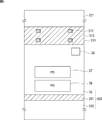
- FIG. 2 is a diagram illustrating a configuration of a conventional imaging device.
- the imaging device shown in FIG. 2 is a CMOS imaging device.
- FIG. 2 is a cross-sectional view of one pixel 20 in the pixel portion of the CMOS imaging device.
- the imaging device 21 includes one organic photoelectric conversion unit 41 stacked in the depth direction in the same pixel, that is, one pixel, and inorganic photoelectric conversion units PD36 and PD37 having two pn junctions. Composed.
- the imaging device 21 has a semiconductor substrate (silicon substrate) 35 on which an inorganic photoelectric conversion unit is formed, and a light receiving surface on which light is incident on the back side of the substrate 35 (upper side of the substrate 35 in the figure). Then, a circuit including a readout circuit and the like is formed on the surface side of the substrate 35. In other words, the imaging device 21 has a light receiving surface on the back side of the substrate 35 and a circuit forming surface formed on the substrate surface side opposite to the light receiving surface.
- the semiconductor substrate 35 is formed of a first conductivity type, for example, an n-type semiconductor substrate.
- an inorganic photoelectric conversion unit having two pn junctions that is, a first photodiode PD36 and a second photodiode PD37 are formed so as to be stacked in the depth direction from the back surface side.
- the first photodiode PD36 and the second photodiode PD37 are formed from the back surface side toward the depth direction (downward in the drawing).
- the first photodiode PD36 is for blue and the second photodiode PD37 is for red.
- the organic photoelectric conversion film 32 is configured such that the upper and lower surfaces of the organic photoelectric conversion film 32 are sandwiched between the upper electrode 31 and the lower electrode 33 on the upper surface of the back surface of the substrate in the region where the first photodiode PD36 and the second photodiode PD37 are formed.
- An organic photoelectric conversion unit 41 for one color is stacked.
- the organic photoelectric conversion unit 36 is for green.
- the upper electrode 31 and the lower electrode 33 are formed of a transparent conductive film such as an indium tin oxide (ITO) film or an indium zinc oxide film.
- ITO indium tin oxide
- the description will be continued assuming that the upper electrode 31 is composed of an oxide semiconductor (ITO) 51 and an aluminum oxide (AlO) thin film 52.
- the description will be continued assuming that the lower electrode 33 is an oxide semiconductor (ITO).
- the organic photoelectric conversion unit 41 is green, the first photodiode PD36 is blue, and the second photodiode PD37 is red.
- the organic photoelectric conversion unit 41 can be red or blue, and the first photodiode PD36 and the second photodiode PD37 can be set to other corresponding colors. In this case, the positions in the depth direction of the first and second photodiodes PD36 and PD37 are set according to the color.
- an organic photoelectric conversion material containing a rhodamine dye, a melocyanine dye, quinacridone, or the like can be used as the organic photoelectric conversion film that performs photoelectric conversion with green wavelength light.
- An organic photoelectric conversion material containing a phthalocyanine dye can be used as the organic photoelectric conversion film that performs photoelectric conversion with red wavelength light.
- an organic photoelectric conversion material containing a coumarin dye, tris-8-hydroxyquinoline Al (Alq3), a melocyanine dye, or the like can be used.
- a transparent lower electrode 33 is formed, and an insulating film 34 for insulating and separating the lower electrode 33 is formed. Then, the organic photoelectric conversion film 32 and the transparent upper electrode 31 thereon are formed on the lower electrode 33.
- a pair of wirings 39 and wirings 40 are formed on the semiconductor substrate 35 in one pixel 20.
- the lower electrode 33 of the organic photoelectric conversion unit 41 is connected to the wiring 39, and the upper electrode 31 is connected to the wiring 40.
- the wiring 39 and the wiring 40 can be formed of, for example, a tungsten (W) plug having an SiO2 or SiN insulating layer in the periphery, a semiconductor layer by ion implantation, or the like in order to suppress a short circuit with Si. .
- the wiring 39 is an n-type semiconductor layer when formed by a semiconductor layer formed by ion implantation. Since the upper electrode draws holes, the p-type can be used.
- an n-type region 38 for charge accumulation is formed on the surface side of the substrate 35.
- the n-type region 38 functions as a floating diffusion part of the organic photoelectric conversion part 41.
- a film having a negative fixed charge can be used as the insulating film 34 on the back surface of the semiconductor substrate 35.
- a film having a negative fixed charge for example, a hafnium oxide film can be used. That is, the insulating film 34 may be formed in a three-layer structure in which a silicon oxide film, a hafnium oxide film, and a silicon oxide film are sequentially formed from the back surface.
- a plurality of pixel transistors corresponding to the organic photoelectric conversion unit 36, the first photodiode PD36, and the second photodiode PD37 are formed on the circuit formation surface on the front surface side of the substrate 35.
- the plurality of pixel transistors the above-described 4-transistor configuration or 3-transistor configuration can be applied.
- a configuration in which pixel transistors are shared can also be applied. In FIG. 2, these transistors are not shown.
- a pixel transistor of the pixel portion is formed on the surface side of the semiconductor substrate 35, and a peripheral circuit such as a logic circuit is formed in the peripheral circuit portion.
- a layer including peripheral circuits is described as a multilayer wiring layer.
- the multilayer wiring layer is provided on the lower side of the substrate 35 in the drawing.
- the back surface side of the semiconductor substrate 35 more specifically, the surface of the upper electrode 31 of the organic photoelectric conversion unit 41 becomes the light receiving surface. Then, an on-chip lens (not shown) is formed on the organic photoelectric conversion unit 41 via a planarizing film (not shown). In this example, no color filter is formed.
- the imaging device 21 is configured as a so-called back-side illumination type imaging device that emits light from the back side of the substrate.
- a fixed negative voltage VL ( ⁇ 0 V) is applied to the lower electrode 33 of the organic photoelectric conversion unit 36 through the required wiring of the multilayer wiring layer, and the lower electrode 33 is applied to the upper electrode 31 during charge accumulation.
- a voltage VU (> VL) higher than the voltage VL, for example, a power supply voltage is applied. That is, the negative voltage VL is applied to the lower electrode 33 on the side close to the semiconductor substrate 35.
- the green wavelength light is photoelectrically converted in the organic photoelectric conversion film 32 having absorption characteristics for the green wavelength light.
- electrons serving as signal charges are attracted to the upper electrode 31 having a high potential VU.
- the hole (hole) of photoelectric conversion is drawn to the lower electrode 33 of the VL to the negative electrode.
- the blue wavelength light is absorbed by the first photodiode PD 36 formed in a shallow place near the back surface of the semiconductor substrate 35, undergoes photoelectric conversion, and signal charges corresponding to blue are accumulated.
- the red wavelength light is absorbed by the second photodiode PD37 formed deep from the back surface of the semiconductor substrate 35, undergoes photoelectric conversion, and signal charges corresponding to red are accumulated.
- transfer transistor When transferring charge, transfer transistor (not shown) turns on. When each transfer transistor is turned on, the accumulated signal charges (electrons) of the organic photoelectric conversion unit 41, the first photodiode PD36, and the second photodiode PD37 are transferred to the corresponding floating diffusion unit (FD). Is done. Thus, the red, green and blue pixel signals are read out to the vertical signal line through the other pixel transistors and output.
- the precursor is reduced with O3, so it is oxidized to form a film.
- O3 during film formation deteriorates and deteriorates the organic photoelectric conversion film 32 and the lower electrode 33.
- the lower electrode 33 needs to use a transparent electrode with a high work function
- the upper electrode 31 needs to use a transparent electrode with a low work function.
- the film is controlled to have a high work function by forming an O-rich film by oxygen plasma treatment.
- the lower electrode 33 when the lower electrode 33 is deteriorated by the influence of O3 during film formation, the work function is lowered, hole transport is hindered, and sensitivity may be lowered. That is, when the lower electrode 33 is altered due to the influence of hydrogen or the like and the work function is lowered, the sensitivity is lowered. Therefore, it is necessary to prevent such a situation.
- FIG. 3 is a diagram showing a configuration of an imaging apparatus having a configuration for protecting the lower electrode 33 from a substance that causes a decrease in work function such as hydrogen.
- the same parts as those of the imaging device 21 shown in FIG. 2 are denoted by the same reference numerals, and the description thereof is omitted as appropriate.
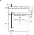
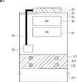
- the imaging apparatus 101 shown in FIG. 3 has a metal thin film 102 on the upper electrode 31. More specifically, a metal thin film 102 is provided below the oxide semiconductor 51 and the aluminum oxide (AlO) thin film 52 constituting the upper electrode 31 and between the AlO thin film 52 and the organic photoelectric conversion unit 41. ing.
- AlO aluminum oxide
- the upper electrode 31 is composed of an oxide semiconductor film, a metal oxide film, and a metal film.
- Al aluminum
- Aluminum has a low work function.
- the work function on the upper electrode 31 side of the organic photoelectric conversion film 41 is preferably set low. Therefore, by providing a film made of a material having a low work function such as aluminum on the upper electrode 31 side of the organic photoelectric conversion portion 41, the work function can be kept low (shallow), and sensitivity can be maintained. Can be improved.
- the metal thin film 102 can prevent intrusion of hydrogen or the like by the metal thin film 102. That is, in this case, the metal thin film 102 can prevent a substance such as hydrogen from entering the organic photoelectric conversion film 32 from the upper electrode 31 side.
- the metal thin film 102 is formed to a thickness of 5 nm or less. With such a thickness, the metal thin film 102 can be provided without impeding light transmission and without causing a decrease in sensitivity.
- the work function of the upper electrode 31 is preferably shallow, even if the oxide semiconductor 51 included in the upper electrode 31 changes due to a substance such as hydrogen and the work function becomes shallow, the sensitivity of the imaging device 101 is improved. There is no such thing as a decline. Therefore, as shown in FIG. 3, the upper electrode 31 may be provided not on the upper side (oxide semiconductor 51) but on the lower side (opposite to the light receiving surface).
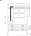
- the upper electrode 31 may be composed of only the metal thin film 112.
- the upper electrode 31 is composed of a metal thin film 112.
- the metal thin film 112 is made of aluminum or the like, it can function as an electrode. Therefore, the metal thin film 112 may be used as the upper electrode 31.
- the upper electrode 31 is preferably transparent and the metal thin film 112 is opaque, it is necessary to configure it as thin as possible and transmit light.
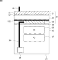
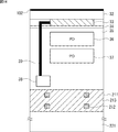
- a metal thin film 102 may be provided above the lower electrode 33 as shown in FIG.
- the imaging device 121 illustrated in FIG. 5 is on the upper side of the lower electrode 33, and a metal thin film 122 is provided between the lower electrode 33 and the organic photoelectric conversion film 32.
- the metal thin film 122 is provided on the lower electrode 33, it is possible to prevent a substance such as hydrogen from entering the lower electrode 33 and deteriorating the lower electrode 33. .
- the metal thin film 122 is provided on the lower electrode 33 side, if the material of the thin film used as the metal thin film 122 is a material having a deep (high) work function, the work function of the lower electrode 33 is deep. It becomes easy to maintain, and the sensitivity of the imaging device 121 can be maintained.
- the lower electrode 33 itself may be composed of the metal thin film 122.
- the metal thin film 122 may be made of a metal having a high work function and function as the lower electrode 33.
- the lower electrode 33 is preferably transparent, and the metal thin film 122 is opaque. Therefore, the lower electrode 33 needs to be configured as thin as possible so as to transmit light.
- Imaging device ⁇ Manufacture of imaging device> The manufacture of the above imaging device will be described. Here, the case where the imaging apparatus 101 shown in FIG. 3 is manufactured will be described as an example. Note that the imaging device 111 shown in FIG. 4 and the imaging device 121 shown in FIG. 5 are basically manufactured through the same processes, and the order of the manufacturing processes is changed, and some processes are added or omitted. It is manufactured by.
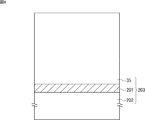
- a so-called SOI substrate 203 in which a silicon layer 35 is formed on a silicon substrate 202 with a silicon oxide film 201 interposed therebetween is prepared.
- the silicon layer 35 corresponds to the semiconductor substrate 35 described above.
- This silicon layer 35 is formed of an n-type silicon layer.
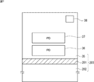
- the first photodiode PD36 for the second color and the second photodiode PD37 for the third color are formed so as to be stacked at different positions in the silicon layer 35.
- the first photodiode PD36 is formed as a photodiode that absorbs blue wavelength light.
- the second photodiode PD37 is formed as a photodiode that absorbs red wavelength light.
- a p-type semiconductor region serving as a hole storage layer and an n-type semiconductor region serving as a charge storage layer are formed by ion implantation on the back side of the silicon layer 35 so that a pn junction is formed. Composed.
- an n-type semiconductor region serving as a charge storage layer is formed by ion implantation so that a pn junction is formed on the surface side of the silicon layer 35.
- the n-type semiconductor region and the underlying p-type semiconductor are formed. It is composed of areas.
- a multilayer wiring layer 211 in which a plurality of layers of wirings 212 are arranged via an interlayer insulating film 213 is formed.
- the first and second photodiodes PD36 and PD37 are photodiodes that absorb blue and red wavelength light.
- the combination is not necessarily limited to two colors of blue and red. It is not a thing.
- a support substrate 221 is pasted on the multilayer wiring layer 211.
- the support substrate 221 for example, a silicon substrate can be used.
- the silicon substrate 202 and the silicon oxide film 201 of the original SOI substrate 203 are removed, and the back surface of the thin silicon layer 35 is exposed.
- an insulating film 34 is formed on the back surface of the silicon layer 35.
- This insulating film 34 is provided in order to reduce the interface state with the silicon layer 35 and to suppress the generation of dark current from the interface between the silicon layer 35 and the insulating film 34, and the interface state should be small. desirable.
- an insulating film 34 for example, a hafnium oxide (HfO 2) film formed by an ALD (atomic layer deposition) method, a silicon oxide (SiO 2) film formed by a plasma CVD (chemical vapor deposition) method, and the like.
- the laminated structure film can be used. Note that the present invention is not limited to the structure and the film formation method described here, and other structures and other film formation methods can be used.
- a wiring 39 that also serves as a light shielding film is formed in the silicon layer 35.
- the wiring 39 is processed so as to leave a portion where light shielding is desired.
- the wiring 39 needs to be in contact with silicon (Si) and is also used as a light-shielding film. Therefore, a laminated film of barrier metal Ti and TiN and tungsten (W) can be used.
- the structure and the material are not necessarily limited.
- a lower electrode 33 that is a lower electrode of the organic photoelectric conversion unit 41 is formed.
- an insulating film such as a SiO2 film formed by a plasma CVD method is used for electrical insulation, and planarization is performed using CMP or the like.
- the lower electrode 33 is required to transmit light, for example, after the ITO film is formed using a sputtering method, patterning is performed using a photolithography technique, and dry etching or wet etching is used. Processed.
- the material of the lower electrode 33 is not limited to ITO, but tin oxide-based SnO2 (dopant added), and zinc oxide-based materials include aluminum zinc oxide (ZnO added with Al as a dopant, for example, AZO), gallium zinc oxide (E.g., Zn added to ZnO as a dopant, such as GZO), indium zinc oxide (ZnO added as an dopant, such as IZO), IGZO, CuI, InSbO4, ZnMgO, CuInO2, MgIn2O4, CdO, ZnSnO3, etc. be able to.
- ZnO added with Al for example, AZO
- gallium zinc oxide E.g., Zn added to ZnO as a dopant, such as GZO
- indium zinc oxide ZnO added as an dopant, such as IZO
- IGZO CuI, InSbO4, ZnMgO, CuInO2, MgIn2O
- the lower electrode 33 is electrically connected to the charge storage layer 38 through the wiring 39. Either the wiring 39 or the lower electrode 33 may be patterned first.
- an organic photoelectric conversion film 32 is formed.
- the organic photoelectric conversion film 32 can be formed of, for example, quinacridone by a vacuum deposition method.
- the organic photoelectric conversion film 32 is laminated on the lower electrode 33 like an electron blocking film / buffer film, a photoelectric conversion film, a hole blocking film, a hole blocking / buffer film, and a work function adjusting film. Also included in this example is a configuration.
- the organic photoelectric conversion film 32 only needs to include at least one of an organic p-type semiconductor and an organic n-type semiconductor, and has a p-type blocking layer, a p-type and n-type co-deposition layer, and an n-type blocking layer.
- a pin bulk heterostructure may also be used.
- any of quinacridone derivatives, naphthalene derivatives, anthracene derivatives, phenanthrene derivatives, tetracene derivatives, pyrene derivatives, perylene derivatives, and fluoranthene derivatives can be used.
- polymers such as phenylene vinylene, fluorene, carbazole, indole, pyrene, pyrrole, picoline, thiophene, acetylene, diacetylene, and derivatives thereof are used.
- metal complex dyes cyanine dyes, merocyanine dyes, phenylxanthene dyes, triphenylmethane dyes, rhodacyanine dyes, xanthene dyes, macrocyclic azaannulene dyes, azulene dyes, naphthoquinone, anthraquinone dyes, anthracene
- a chain compound condensed with condensed polycyclic aromatic and aromatic or heterocyclic compounds such as pyrene, or two nitrogen-containing compounds such as quinoline, benzothiazole, benzoxazole, etc.
- a squarylium group and a croconic methine group as a binding chain It is possible to use a cyanine-like dye or the like bonded by a heterocyclic ring or a squarylium group and a croconite methine group.
- the metal complex dye may be a dithiol metal complex dye, a metal phthalocyanine dye, a metal porphyrin dye, or a ruthenium complex dye. Other than those exemplified here may be used.
- the organic photoelectric conversion film 32 can also be formed by a coating method.
- the upper electrode 31 is formed on the organic photoelectric conversion film 32.
- the characteristics of the organic photoelectric conversion film 32 may vary due to the influence of moisture, oxygen, hydrogen, and the like. Therefore, the upper electrode 31 is formed in a vacuum consistent with the organic photoelectric conversion film 32.
- the upper electrode 31 is formed of the metal thin film 102, the AlO thin film 52, and the oxide semiconductor 51 as described with reference to FIG. 3.
- the metal thin film 102 can be an Al film formed of Al (aluminum), and can be formed by, for example, a vacuum deposition method.
- Al is a material having a shallow work function of about 4.3 eV, and is one of materials suitable as a material in contact with the organic photoelectric conversion film 32.
- materials that can be used as the metal thin film 102 include indium (In), silver (Ag), gold (Au), zinc (Zn), lithium (Li), tin (Sn), and antimony (Sb). , Magnesium (Mg), cadmium (Cd), calcium (Ca), potassium (K), rubidium (Rb), cesium (Cs), strontium (Sr), barium (Ba), cerium (Ce), yttrium (Y) , Hafnium (Hf), nickel (Ni), gallium (Ga), titanium (Ti), and the like.
- metal thin film 102 may be configured as a plurality of compounds, or a compound of a material listed here and a material not listed may be a metal thin film. It may be 102.
- an AlO film 52 is formed.
- the oxide semiconductor 51 is formed by sputtering, for example, after the metal thin film 102 is formed of Al, the metal thin film 102 is oxidized by the energy of the sputtered particles, and the AlO thin film 52 is easily formed by several nm. be able to.
- the AlO thin film 52 is formed to a thickness of 20 nm or less.
- the AlO thin film 52 is formed by oxidizing Al with the energy of sputtered particles.
- the present invention is not limited to this, and it may be formed using an ALD method, a CVD method, or the like. good.
- the AlO thin film 52 is an insulating film, generally the photoelectric conversion area (the area of the upper electrode 31) is sufficiently large with respect to the film thickness of the AlO film 52, so that sufficient conduction is achieved with a thermal diffusion component. Can do.
- the Al film and the AlO film formed in this way are known to have high passivation properties against hydrogen, shielding the hydrogen generated during the process and suppressing the work function variation of the lower electrode 33. Can do.
- the remaining metal thin film 102 is desirably 5 nm or less. This is because Al is a material with high light shielding properties, but sufficient light transmittance can be secured in a thin film region of 5 nm or less.
- an oxide semiconductor 51 constituting a part of the upper electrode 31 is formed.
- the oxide semiconductor 51 is also required to be transparent with respect to visible light.
- ITO is described as an example.
- the oxide semiconductor 51 is not limited to ITO.
- tin oxide-based SnO 2 dopant added
- aluminum zinc oxide (Al is added to ZnO as a dopant, for example, AZO)
- gallium zinc oxide Ga is added to ZnO as a dopant, for example, GZO
- indium zinc oxide (InO is added to ZnO as a dopant
- IZO IGZO, CuI, InSbO4, ZnMgO, CuInO2, MgIn2O4, CdO, ZnSnO3, or the like can also be used.
- the upper electrode 31 is formed, patterning is performed using, for example, a photolithography technique. Then, the upper electrode 31 and the organic photoelectric conversion film 32 are processed using dry etching. Thereafter, post-processing such as ashing and organic cleaning is performed to remove deposits and residues.
- patterning is performed by photolithography and dry etching, but patterning can also be performed using a shadow mask or the like.
- a wiring 40 for electrical connection with a passivation film (not shown) and the upper electrode 31 is formed.
- the side wall of the organic photoelectric conversion film 32 is in direct contact with the passivation film, but the lower electrode 33 and the passivation film are sufficiently separated from each other, and thus are hardly affected.
- the wiring 40 include tungsten (W), barrier metal Ti, TiN, and aluminum (Al), but are not limited thereto.
- the wiring 40 is formed by patterning using, for example, a photolithography technique, processing using dry etching, post-processing such as ashing and organic cleaning, and removing deposits and residues. Thereafter, although not shown, a planarizing film, an on-chip lens, and the like are formed.
- the photographing apparatus 101 is manufactured in this way, hydrogen during the manufacturing process can be shielded from entering the lower electrode 33, and the work function of the lower electrode 33 is prevented from fluctuating. can do.
- CMOS imager structure in which blue and red photoelectric conversion regions are stacked in silicon and a green photoelectric conversion part is formed on the upper layer of silicon has been described as an example.
- the scope of technology is not limited.
- the backside illuminated CMOS imager structure has been described as an example, but the scope of application of the present technology is not limited to such a structure.
- FIG. 16 is a diagram illustrating a configuration of an imaging apparatus according to the second embodiment.
- the same reference numerals are given to the same parts as those of the imaging apparatus 101 illustrated in FIG.
- the metal thin film 102 of the imaging device 101 (FIG. 3) in the first embodiment is configured in a film shape, but the imaging device 301 in the second embodiment is not configured in a film shape. Different.
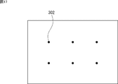
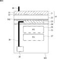
- the metal electrode 302 is described. As shown in FIG. 16, the metal electrode 302 is provided below the AlO film 52, provided on the organic photoelectric conversion film 32 side, and provided in a scattered manner.
- the metal electrode 302 constituting the upper electrode 31 can be configured not to be a film but to remain at the atomic level. Also in this configuration, since AlO exists as the AlO film 52, the passivation property is secured.
- the metal electrode 302 exists as shown in FIG.
- the metal electrode 302 may be spherical or quadrangular, and the shape is not particularly limited. Further, the metal electrodes 302 may be arranged at equal intervals or may be arranged at random intervals.
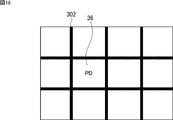
- the metal electrode 302 may be configured in a lattice shape.
- the metal electrode 302 may be formed so that the first photodiode PD36 is positioned in the lattice.
- the metal electrode 302 may be formed so that the metal electrode 302 is positioned between the photodiodes.
- the metal electrode 302 When the metal electrode 302 is configured in a lattice shape, the metal electrode 302 can be provided with a light shielding function. That is, the metal electrode 302 is formed in a lattice shape, and the metal electrode 302 is formed with such a width and thickness as to obtain a light shielding function, and at a position where the amount of light incident on the photodiode or the like does not decrease. Thus, the metal electrode 302 can function as a light shielding film (light shielding wall).
- the metal electrode 302 when the metal electrode 302 is formed to have a predetermined shape such as a lattice shape, it can be formed by applying patterning, a shadow mask, or the like.
- FIG. 19 is a diagram illustrating a configuration of an imaging apparatus according to the third embodiment.
- parts similar to those of the imaging apparatus 101 illustrated in FIG. 3 are denoted by the same reference numerals, and description thereof is omitted.
- the imaging device 401 in the third embodiment includes a hole blocking layer.
- the hole blocking layer 402 is provided as a part of the upper electrode 31, is provided below the metal thin film 102, and is provided between the metal thin film 102 and the organic photoelectric change film 32. It has been.
- the hole blocking layer 402 is made of a material such as lithium fluoride (LiF) or magnesium oxide (MgO), and the same effect can be obtained even when the upper electrode 31 having the metal thin film 102 is laminated, and the dark current is reduced. You can also.
- LiF lithium fluoride
- MgO magnesium oxide
- the hole blocking layer 402 in the imaging device 101 shown in FIG. 3 was shown here, you may provide the hole blocking layer 402 in the imaging device 111 shown in FIG. Although not shown, when the hole blocking layer 402 is provided in the imaging device 111, the hole blocking layer 402 is provided between the metal thin film 122 and the organic photoelectric change film 32.
- the hole blocking layer 402 may be provided in the imaging device 121 shown in FIG. Although not shown, when the hole blocking layer 402 is provided in the imaging device 121, the hole blocking layer 402 is provided between the AlO film 52 and the organic photoelectric conversion film 32.
- the hole blocking layer 402 may be provided in the imaging device 301 shown in FIG. Although not shown, when the hole blocking layer 402 is provided in the imaging device 301, it is provided between the AlO film 52 and the organic photoelectric conversion film 32. In this case, the metal electrode 302 may be provided in the same layer as the hole blocking layer 402, or the metal electrode 302 may be provided between the hole blocking layer 402 and the organic photoelectric change film 32.
- FIG. 20 is a diagram illustrating a configuration of an imaging device according to the fourth embodiment.
- the same parts as those of the imaging device 101 shown in FIG. 20 the same parts as those of the imaging device 101 shown in FIG.
- the imaging device 501 in the fourth embodiment includes an enthalpy control layer.
- an enthalpy control layer 502 is provided between the organic photoelectric change film 32 and the lower electrode 33 above the lower electrode 33.
- the enthalpy control layer 502 is formed as an oxide film containing, for example, cadmium (Cd), copper (Cu), lead (Pb), palladium (Pd), and the like.
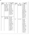
- FIG. 21 lists materials that can be used as the enthalpy control layer 502. As shown in FIG.
- the enthalpy control layer 502 includes Ag2O, CoO, Co3O4, CdO, Cs2O, CuO, Cu2O, GeO (c), GeO2 (cl), GeO2 (c2), NiO (c), PbO ( c), PbO2 (c2), PbO2 (c), PdO (c), Rb2O (c), Rb2O2 (c), SeO2 (c), SeO3 (c), TeO2 (C), Tl2O (c), Tl2O3 ( c).
- a material that can be used for the lower electrode 33 is described in the column “transparent electrode”, and a substance name (element symbol) that composes the material described in the column “transparent electrode” is written in the column “composition”.
- the substance name (element symbol) constituting the material that can be used as the material of the enthalpy control layer 502 is described.
- the numerical value described in association with each element symbol is a numerical value of the standard generation enthalpy.
- the lower electrode 33 is prevented from being altered and the work function is prevented from becoming shallow, as in the imaging devices in the first to third embodiments. Is possible.
- the enthalpy control layer 502 is made of a copper oxide (CuO) film
- the standard generation enthalpy of copper oxide from FIG. 21, -157.3
- the tin oxide Since it is higher than the standard generation enthalpy of SnO) (-280.71 from FIG. 21), the enthalpy control layer 502 is selectively reduced.
- the enthalpy control layer 502 is about 5 nm.
- the enthalpy control layer 502 on the lower electrode 33, it is possible to prevent a substance such as hydrogen from entering the lower electrode 33 and changing the work function of the lower electrode 33.
- the above-described imaging device includes an image capturing unit (photoelectric conversion) such as an imaging device such as a digital still camera and a video camera, a portable terminal device having an imaging function such as a mobile phone, and a copying machine using the imaging device for an image reading unit.
- an image capturing unit photoelectric conversion
- an imaging device such as a digital still camera and a video camera
- a portable terminal device having an imaging function such as a mobile phone
- a copying machine using the imaging device for an image reading unit for an image reading unit.
- the present invention can be applied to all electronic devices using semiconductor devices.
- FIG. 22 is a block diagram illustrating an example of a configuration of an electronic apparatus according to the present technology, for example, an imaging apparatus.
- an imaging apparatus 1000 according to the present technology includes an optical system including a lens group 1001 and the like, an imaging element (imaging device) 1002, a DSP circuit 1003, a frame memory 1004, a display device 1005, a recording device 1006, and an operation.
- a DSP circuit 1003, a frame memory 1004, a display device 1005, a recording device 1006, an operation system 1007, and a power supply system 1008 are connected to each other via a bus line 1009.
- the lens group 1001 takes in incident light (image light) from a subject and forms an image on the imaging surface of the imaging element 1002.
- the imaging element 1002 converts the amount of incident light imaged on the imaging surface by the lens group 1001 into an electrical signal in units of pixels and outputs it as a pixel signal.
- the display device 1005 includes a panel type display device such as a liquid crystal display device or an organic EL (electroluminescence) display device, and displays a moving image or a still image captured by the image sensor 1002.
- the recording device 1006 records a moving image or a still image captured by the image sensor 1002 on a recording medium such as a DVD (Digital Versatile Disk) or HDD (Hard Disk Drive).
- the operation system 1007 issues operation commands for various functions of the imaging apparatus under operation by the user.
- the power supply system 1008 appropriately supplies various power supplies serving as operation power supplies for the DSP circuit 1003, the frame memory 1004, the display device 705, the recording device 1006, and the operation system 1007 to these supply targets.
- the imaging apparatus having the above-described configuration can be used as an imaging apparatus such as a video camera, a digital still camera, and a camera module for mobile devices such as a mobile phone.
- the imaging device described above can be used as the imaging element 1002.
- FIG. 23 is a diagram illustrating a usage example in which the above-described imaging device is used.
- the imaging device described above can be used in various cases for sensing light such as visible light, infrared light, ultraviolet light, and X-rays as follows.
- Devices for taking images for viewing such as digital cameras and mobile devices with camera functions
- Devices used for traffic such as in-vehicle sensors that capture the back, surroundings, and interiors of vehicles, surveillance cameras that monitor traveling vehicles and roads, and ranging sensors that measure distances between vehicles, etc.
- Equipment used for home appliances such as TVs, refrigerators, air conditioners, etc. to take pictures and operate the equipment according to the gestures ⁇ Endoscopes, equipment that performs blood vessel photography by receiving infrared light, etc.
- Equipment used for medical and health care ⁇ Security equipment such as security surveillance cameras and personal authentication cameras ⁇ Skin measuring instrument for photographing skin and scalp photography Such as a microscope to do beauty Equipment used for sports-Equipment used for sports such as action cameras and wearable cameras for sports applications-Used for agriculture such as cameras for monitoring the condition of fields and crops apparatus
- this technology can also take the following structures.
- An organic photoelectric conversion film An upper electrode provided on the organic photoelectric change film; A lower electrode provided under the organic photoelectric change film; An imaging device comprising: a metal thin film provided between the organic photoelectric change film and the upper electrode or between the organic photoelectric change film and the lower electrode.
- the metal thin film is provided between the organic photoelectric change film and the upper electrode, The imaging device according to (1), wherein the upper electrode includes an oxide semiconductor, a metal oxide, and the metal thin film.
- the metal oxide is aluminum oxide (AlO), and the metal thin film is aluminum (Al).
- the metal thin film includes aluminum (Al), indium (In), silver (Ag), gold (Au), zinc (Zn), lithium (Li), tin (Sn), antimony (Sb), magnesium (Mg), Cadmium (Cd), calcium (Ca), potassium (K), rubidium (Rb), cesium (Cs), strontium (Sr), barium (Ba), cerium (Ce), yttrium (Y), hafnium (Hf),
- the imaging device according to any one of (1) to (3), which is configured of any one of nickel (Ni), gallium (Ga), and titanium (Ti).
- the upper electrode and the lower electrode are made of ITO, tin oxide-based SnO2, zinc oxide-based aluminum zinc oxide, gallium zinc oxide, indium zinc oxide, IGZO, CuI, InSbO4, ZnMgO, CuInO2, MgIn2O4, CdO.
- the imaging device according to any one of (1) to (4), configured by any one of ZnSnO3 and ZnSnO3.
- the organic photoelectric conversion film is composed of any one of quinacridone derivatives, naphthalene derivatives, anthracene derivatives, phenanthrene derivatives, tetracene derivatives, pyrene derivatives, perylene derivatives, or fluoranthene derivatives.
- the organic photoelectric conversion film is a polymer of phenylene vinylene, fluorene, carbazole, indole, pyrene, pyrrole, picoline, thiophene, acetylene, diacetylene or derivatives thereof, metal complex dye, cyanine dye, merocyanine dye, phenylxanthene Dyes, triphenylmethane dyes, rhodacyanine dyes, xanthene dyes, macrocyclic azaannulene dyes, azulene dyes, naphthoquinones, anthraquinone dyes, condensed polycyclic aromatics such as anthracene and pyrene, and aromatic or heterocyclic compounds Condensed chain compounds, or two nitrogen-containing heterocycles such as quinoline, benzothiazole, and benzoxazole having a squarylium group and a croconic meth
- the imaging device consists either in bound cyanine similar dyes,
- the metal complex dye is any one of a dithiol metal complex dye, a metal phthalocyanine dye, a metal porphyrin dye, or a ruthenium complex dye.
- the metal thin film has a thickness of 5 nm or less.
- the metal thin film is formed in a spherical shape or a predetermined shape, and is scattered at equal intervals or randomly.
- the imaging device according to any one of (1) to (9), further including a hole blocking layer between the metal thin film and the organic photoelectric conversion film.
- the imaging apparatus according to (1) further including an enthalpy control layer together with the metal thin film or instead of the metal thin film.
- the enthalpy control layer includes Ag2O, CoO, Co3O4, CdO, Cs2O, CuO, Cu2O, GeO (c), GeO2 (cl), GeO2 (c2), NiO (c), PbO (c), PbO2 (c2), PbO2 (c), PdO (c), Rb2O (c), Rb2O2 (c), SeO2 (c), SeO3 (c), TeO2 (C), Tl2O (c), Tl2O3 (c)
Landscapes
- Physics & Mathematics (AREA)
- Electromagnetism (AREA)
- Solid State Image Pick-Up Elements (AREA)
Abstract
本技術は、水素などの物質の侵入を防ぎ、性能が変化するようなことを防ぐことができるようにする撮像装置、製造装置、製造方法に関する。 有機光電変換膜と、有機光電変化膜の上部に設けられた上部電極と、有機光電変化膜の下部に設けられた下部電極と、有機光電変化膜と上部電極の間、または有機光電変化膜と下部電極との間に設けられた金属薄膜とを備える。金属薄膜は、有機光電変化膜と上部電極の間に設けられ、上部電極は、酸化物半導体、金属酸化物、および金属薄膜から構成されている。本技術は、縦型分光の撮像装置に適用できる。
Description
本技術は、撮像装置、製造装置、製造方法に関する。詳しくは、水素による影響を低減させるのに用いて好適な撮像装置、製造装置、製造方法に関する。
近年、CCDイメージセンサCCD(Charge Coupled Device)イメージセンサやCMOS(Complementary Metal Oxide Semiconductor)では、画素サイズが縮小しつつある。そのために、単位画素に入射するフォトン数の減少にために感度が低下し、S/Nが低下してしまう。また、現在広く用いられている、赤、緑および青の画素を平面上に並べた画素配列、例えば原色カラーフィルタを用いたベイヤー配列の場合、例えば、赤画素では、緑と青の光がカラーフィルタを透過せず光電変換に用いられないために、感度の面で損失している。また、画素間の補間処理が行われると、色信号を作ることに伴う偽色が発生する可能性があった。
光電変換層を縦方向に3層積層し、1画素で3色の光電変換信号を得るイメージセンサが提案されている。特許文献1では、そのような1画素で3色の光電変換層を積層する構造として、例えば、緑色光を検出してこれに応じた信号電荷を発生する光電変換部をシリコン基板上方に設け、シリコン基板内に積層した2つのフォトダイオードで青色光と赤色光を検出するというセンサが提案されている。
また、特許文献2では、光電変換膜1層をシリコン基板上方に設け、シリコン基板中で2色の光電変換部を有する構造において、回路形成面が受光面とは反対側に形成された裏面照射型について提案されている。裏面照射型に有機光電変換層を形成する場合、無機光電変換部と有機光電変換部の間に回路、配線等が形成されないので、同一画素内の無機光電変換部と有機光電変換部の距離を近づけることが可能となる。そのため、各色のF値依存を抑制することができ、各色間の感度の変動を抑制することができる。
有機光電変換膜は、一般的に水や酸素に弱いため、有機光電変換膜上層に封止構造を形成する必要がある。例えば特許文献3では、スパッタ法で製膜したSiN膜とALD法で製膜したAlO膜を積層した封止構造を形成することが提案されている。
しかしながら、このような封止膜を形成すると、ALD法はプリカーサとしてTMA(トリメチルアルミニウム)などの有機金属を用いる必要があり、プリカーサ中の水素が、上部と下部の透明電極まで拡散してしまう可能性がある。拡散してしまう結果、上部電極だけでなく下部電極も還元されてしまい、仕事関数が浅くなり、有機光電変換効率が劣化する可能性がある。
下部電極の仕事関数は深く、上部電極の仕事関数は浅くすることが望ましい。これは下部電極からの電子注入障壁をあげて暗電流を減らすこと、および内部電界を増加してキャリアの取り出し効率を向上することができるためである。
よって、上記したように、プリカーサ中の水素が、下部の透明電極まで拡散し、下部電極が還元され、仕事関数が浅くなり、有機光電変換効率が劣化するようなことを防ぐことが望まれている。
本技術は、このような状況に鑑みてなされたものであり、水素が拡散することで、仕事関数が変換し、有機光電変換効率が劣化するようなことを防ぐことができるようにするものである。
本技術の一側面の撮像装置は、有機光電変換膜と、前記有機光電変化膜の上部に設けられた上部電極と、前記有機光電変化膜の下部に設けられた下部電極と、前記有機光電変化膜と前記上部電極の間、または前記有機光電変化膜と前記下部電極との間に設けられた金属薄膜とを備える。
前記金属薄膜は、前記有機光電変化膜と前記上部電極の間に設けられ、前記上部電極は、酸化物半導体、金属酸化物、および前記金属薄膜から構成されているようにすることができる。
前記金属酸化物は、酸化アルミニウム(AlO)であり、前記金属薄膜はアルミニウム(Al)であるようにすることができる。
前記金属薄膜は、アルミニウム(Al)、インジウム(In)、銀(Ag)、金(Au)、亜鉛(Zn)、リチウム(Li)、スズ(Sn)、アンチモン(Sb)、マグネシウム(Mg)、カドミウム(Cd)、カルシウム(Ca)、カリウム(K)、ルビジウム(Rb)、セシウム(Cs)、ストロンチウム(Sr)、バリウム(Ba)、セリウム(Ce)、イットリウム(Y)、ハフニウム(Hf)、ニッケル(Ni)、ガリウム(Ga)、チタン(Ti)のいずれかで構成されているようにすることができる。
前記上部電極と前記下部電極は、ITO、酸化スズ系のSnO2、酸化亜鉛系材料のアルミニウム亜鉛酸化物、ガリウム亜鉛酸化物、インジウム亜鉛酸化物、IGZO、CuI、InSbO4、ZnMgO、CuInO2、MgIn2O4、CdO、ZnSnO3のいずれかで構成されているようにすることができる。
前記有機光電変換膜は、キナクリドン誘導体、ナフタレン誘導体、アントラセン誘導体、フェナントレン誘導体、テトラセン誘導体、ピレン誘導体、ペリレン誘導体、またはフルオランテン誘導体のいずれかで構成されているようにすることができる。
前記有機光電変換膜は、フェニレンビニレン、フルオレン、カルバゾール、インドール、ピレン、ピロール、ピコリン、チオフェン、アセチレン、ジアセチレンの重合体やその誘導体、金属錯体色素、シアニン系色素、メロシアニン系色素、フェニルキサンテン系色素、トリフェニルメタン系色素、ロダシアニン系色素、キサンテン系色素、大環状アザアヌレン系色素、アズレン系色素、ナフトキノン、アントラキノン系色素、アントラセン、ピレン等の縮合多環芳香族および芳香環ないし複素環化合物が縮合した鎖状化合物、または、スクアリリウム基およびクロコニツクメチン基を結合鎖として持つキノリン、ベンゾチアゾール、ベンゾオキサゾール等の二つの含窒素複素環、または、スクアリリウム基およびクロコニツクメチン基により結合したシアニン系類似の色素のいずれかで構成され、前記金属錯体色素は、ジチオール金属錯体系色素、金属フタロシアニン色素、金属ポルフィリン色素、またはルテニウム錯体色素のいずれかであるようにすることができる。
前記金属薄膜は、5nm以下の厚さであるようにすることができる。
前記金属薄膜は、球状、または所定の形状で構成され、等間隔、またはランダムに点在しているようにすることができる。
前記金属薄膜と前記有機光電変換膜との間にホールブロッキング層をさらに備えるようにすることができる。
前記金属薄膜とともに、または前記金属薄膜の代わりに、エンタルピー制御層を備えるようにすることができる。
前記エンタルピー制御層は、前記有機光電変換膜と前記下部電極との間に設けられるようにすることができる。
前記エンタルピー制御層は、Ag2O,CoO,Co3O4,CdO,Cs2O,CuO,Cu2O,GeO(c),GeO2(cl),GeO2(c2),NiO(c),PbO(c),PbO2(c2),PbO2(c),PdO(c),Rb2O(c),Rb2O2(c),SeO2(c),SeO3(c),TeO2 (C),Tl2O(c),Tl2O3(c)のいずれかで構成されているようにすることができる。
本技術の一側面の製造装置は、有機光電変換膜を形成し、前記有機光電変化膜の上部に上部電極を形成し、前記有機光電変化膜の下部に下部電極を形成し、前記有機光電変化膜と前記上部電極の間、または前記有機光電変化膜と前記下部電極との間に金属薄膜を形成する。
前記金属薄膜を、蒸着により形成するようにすることができる。
前記金属薄膜を、前記有機光電変化膜と前記上部電極の間に形成し、前記上部電極を、酸化物半導体、金属酸化物、および前記金属薄膜を積層して形成し、前記金属酸化物を、前記酸化物半導体成膜時に酸化させることで形成するようにすることができる。
前記金属薄膜を、球状、または所定の形状で形成し、等間隔、またはランダムに点在するように形成するようにすることができる。
前記金属薄膜と前記有機光電変換膜との間に、ホールブロッキング層をさらに形成するようにすることができる。
前記金属薄膜とともに、または前記金属薄膜の代わりに、エンタルピー制御層を形成するようにすることができる。
本技術の一側面の製造方法は、有機光電変換膜を形成し、前記有機光電変化膜の上部に上部電極を形成し、前記有機光電変化膜の下部に下部電極を形成し、前記有機光電変化膜と前記上部電極の間、または前記有機光電変化膜と前記下部電極との間に金属薄膜を形成するステップを含む。
本技術の一側面の撮像装置においては、有機光電変換膜と、有機光電変化膜の上部に設けられた上部電極と、有機光電変化膜の下部に設けられた下部電極と、有機光電変化膜と上部電極の間、または有機光電変化膜と下部電極との間に設けられた金属薄膜とが備えられる。
本技術の一側面の製造装置および製造方法は、前記撮像装置を製造する。
本技術の一側面によれば、水素が拡散することで、仕事関数が変換し、有機光電変換効率が劣化するようなことを防ぐことができる。
なお、ここに記載された効果は必ずしも限定されるものではなく、本開示中に記載されたいずれかの効果であってもよい。
以下に、本技術を実施するための形態(以下、実施の形態という)について説明する。なお、説明は、以下の順序で行う。
1.撮像装置の構成
2.従来の撮像装置の構成
3.第1の撮像装置の構成
4.撮像装置の製造
5.第2の撮像装置の構成
6.第3の撮像装置の構成
7.第4の撮像装置の構成
8.電子機器の構成
9.撮像装置の使用例
1.撮像装置の構成
2.従来の撮像装置の構成
3.第1の撮像装置の構成
4.撮像装置の製造
5.第2の撮像装置の構成
6.第3の撮像装置の構成
7.第4の撮像装置の構成
8.電子機器の構成
9.撮像装置の使用例
<撮像装置の構成>
図1に、本実施の形態に適用されるCMOS撮像装置の一例の概略構成を示す。本例の撮像装置1は、図1に示すように、半導体基板11、例えばシリコン基板に光電変換部を含む複数の画素2が規則的に2次元的に配列された画素部(いわゆる撮像領域)3と、周辺回路部とを有して構成される。画素2は、光電変換部と、複数の画素トランジスタ(いわゆるMOSトランジスタ)を有して成る。
図1に、本実施の形態に適用されるCMOS撮像装置の一例の概略構成を示す。本例の撮像装置1は、図1に示すように、半導体基板11、例えばシリコン基板に光電変換部を含む複数の画素2が規則的に2次元的に配列された画素部(いわゆる撮像領域)3と、周辺回路部とを有して構成される。画素2は、光電変換部と、複数の画素トランジスタ(いわゆるMOSトランジスタ)を有して成る。
複数の画素トランジスタは、例えば転送トランジスタ、リセットトランジスタおよび増幅トランジスタの3つのトランジスタで構成することができる。その他、選択トランジスタ追加して4つのトランジスタで構成することもできる。単位画素の等価回路は通常と同様であるので、詳細説明は省略する。また、画素としては、複数の光電変換部が転送トランジスタを除く他の画素トランジスタを共有し、且つフローティングディフージョンを共有する、いわゆる画素共有構造を適用することもできる。
周辺回路部は、垂直駆動回路4と、カラム信号処理回路5と、水平駆動回路6と、出力回路7と、制御回路8などを有して構成される。
制御回路8は、入力クロックと、動作モードなどを指令するデータを受け取り、また撮像装置の内部情報などのデータを出力する。すなわち、制御回路8では、垂直同期信号、水平同期信号およびマスタクロックに基づいて、垂直駆動回路4、カラム信号処理回路5および水平駆動回路6などの動作の基準となるクロック信号や制御信号を生成する。そして、これらの信号を垂直駆動回路4、カラム信号処理回路5および水平駆動回路6等に入力する。
垂直駆動回路4は、例えばシフトレジスタによって構成され、画素駆動配線を選択し、選択された画素駆動配線に画素を駆動するためのパルスを供給し、行単位で画素を駆動する。すなわち、垂直駆動回路4は、画素領域3の各画素2を行単位で順次垂直方向に選択走査し、垂直信号線9を通して各画素2の光電変換素子となる例えばフォトダイオードにおいて受光量に応じて生成した信号電荷に基づく画素信号をカラム信号処理回路5に供給する。
カラム信号処理回路5は、画素2の例えば列ごとに配置されており、1行分の画素2から出力される信号を画素列ごとにノイズ除去などの信号処理を行う。すなわちカラム信号処理回路5は、画素2固有の固定パターンノイズを除去するためのCDSや、信号増幅、AD変換等の信号処理を行う。カラム信号処理回路5の出力段には水平選択スイッチ(図示せず)が水平信号線10との間に接続されて設けられる。
水平駆動回路6は、例えばシフトレジスタによって構成され、水平走査パルスを順次出力することによって、カラム信号処理回路5の各々を順番に選択し、カラム信号処理回路5の各々から画素信号を水平信号線10に出力させる。
出力回路7は、カラム信号処理回路5の各々から水平信号線10を通して順次に供給される信号に対し、信号処理を行って出力する。例えば、バッファリングだけする場合もあるし、黒レベル調整、列ばらつき補正、各種デジタル信号処理などが行われる場合もある。入出力端子12は、外部と信号のやりとりをする。
<従来の撮像装置の構成>
本技術を適用した撮像装置と、従来の撮像装置との差異を明確にするために、まず図2を参照し、従来の撮像装置について説明を加える。図2は、従来の撮像装置の構成を示す図である。図2に示した撮像装置は、CMOS撮像装置である。同図は、CMOS撮像装置の画素部における1つの画素20の断面図である。
本技術を適用した撮像装置と、従来の撮像装置との差異を明確にするために、まず図2を参照し、従来の撮像装置について説明を加える。図2は、従来の撮像装置の構成を示す図である。図2に示した撮像装置は、CMOS撮像装置である。同図は、CMOS撮像装置の画素部における1つの画素20の断面図である。
撮像装置21は、同一の画素、すなわち1つの画素内に、深さ方向に積層した、1つの有機光電変換部41と、2つのpn接合を有する無機光電変換部PD36およびPD37とを有して構成される。
より詳しくは、撮像装置21は、無機光電変換部が形成される半導体基板(シリコン基板)35を有し、基板35の裏面側(図中基板35の上側)に光が入射される受光面が形成され、基板35の表面側に読み出し回路等を含む回路が形成される。すなわち撮像装置21では、基板35の裏面側の受光面と、受光面とは反対側の基板表面側に形成された回路形成面とを有する。半導体基板35は、第1導電型、例えばn型の半導体基板で構成される。
半導体基板35内には、裏面側から深さ方向に積層されるように、2つのpn接合を有する無機光電変換部、すなわち第1フォトダイオードPD36と第2フォトダイオードPD37が形成される。半導体基板35内では、裏面側から深さ方向(図中、下方向)に向かって、第1フォトダイオードPD36が形成され、第2フォトダイオードPD37が形成される。
本例では、第1フォトダイオードPD36が青色用となり、第2フォトダイオードPD37が赤色用となる。
一方、第1フォトダイオードPD36および第2フォトダイオードPD37が形成された領域の基板裏面の上層に、有機光電変換膜32がその上下両面を上部電極31と下部電極33で挟まれて構成された第1色用の有機光電変換部41が積層される。本例では有機光電変換部36が緑色用となる。上部電極31および下部電極33は、例えば、酸化インジウム錫(ITO)膜、酸化インジウム亜鉛膜等の透明導電膜で形成される。
ここでは、上部電極31は、酸化物半導体(ITO)51と酸化アルミニウム(AlO)薄膜52から構成されているとして説明を続ける。また下部電極33は、酸化物半導体(ITO)であるとして説明を続ける。
ここでは、色の組合せとして、有機光電変換部41を緑色、第1フォトダイオードPD36を青色、第2フォトダイオードPD37を赤色としたが、その他の色の組合せも可能である。例えば、有機光電変換部41を赤色、あるいは青色とし、第1フォトダイオードPD36および第2フォトダイオードPD37を、その他の対応する色に設定することができる。この場合、色に応じて第1、第2フォトダイオードPD36、PD37の深さ方向の位置が設定される。
緑の波長光で光電変換する有機光電変換膜としては、例えばローダーミン系色素、メラシアニン系色素、キナクリドン等を含む有機光電変換材料を用いることができる。赤の波長光で光電変換する有機光電変換膜としては、フタロシアニン系色素を含む有機光電変換材料を用いることができる。青の波長光で光電変換する有機光電変換膜としては、クマリン系色素、トリス-8-ヒドリキシキノリンAl(Alq3)、メラシアニン系色素等を含む有機光電変換材料を用いることができる。
有機光電変換部41では、透明の下部電極33が形成され、下部電極33を絶縁分離するための絶縁膜34が形成される。そして、下部電極33上に有機光電変換膜32とその上の透明の上部電極31が形成される。
1つの画素20内における半導体基板35には、1対の配線39と配線40が形成される。有機光電変換部41の下部電極33は、配線39に接続され、上部電極31は、配線40に接続される。
配線39と配線40としては、例えば、Siとの短絡を抑制するために、SiO2もしくは、SiN絶縁層を周辺に有するタングステン(W)プラグ、あるいは、イオン注入による半導体層等により形成することができる。本例では信号電荷を電子としているので、配線39は、イオン注入による半導体層で形成する場合、n型半導体層となる。上部電極はホールを引き抜くのでp型を用いることができる。
本例では、基板35の表面側に電荷蓄積用のn型領域38が形成される。このn型領域38は、有機光電変換部41のフローティングディフージョン部として機能する。
半導体基板35の裏面上の絶縁膜34としては、負の固定電荷を有する膜を用いることができる。負の固定電荷を有する膜としては、例えば、ハフニウム酸化膜を用いることができる。すなわち、この絶縁膜34は、裏面より順次シリコン酸化膜、ハフニウム酸化膜およびシリコン酸化膜を成膜した3層構造にて形成するようにしても良い。
基板35の表面側の回路形成面では、有機光電変換部36、第1フォトダイオードPD36、第2フォトダイオードPD37のそれぞれに対応する複数の画素トランジスタが形成される。複数の画素トランジスタとしては、前述の4トランジスタ構成、3トランジスタ構成を適用できる。また、画素トランジスタを共有した構成も適用できる。図2では、これらのトランジスタは図示していない。
なお、図示しないが、半導体基板35の表面側では、画素部の画素トランジスタが形成されると共に、周辺回路部において、ロジック回路等の周辺回路が形成される。周辺回路などを含む層を多層配線層と記述する。多層配線層は、図2には記載していないが、基板35の図中下側に設けられている。
半導体基板35の裏面側、より詳しくは、有機光電変換部41の上部電極31の面が受光面となる。そして、有機光電変換部41上に平坦化膜(不図示)を介して、オンチップレンズ(不図示)が形成される。本例ではカラーフィルタが形成されない。
撮像装置21の動作(駆動方法)を説明する。この撮像装置21は、基板裏面側から光が照射される、いわゆる裏面照射型の撮像装置として構成される。本例においては、有機光電変換部36の下部電極33に、多層配線層の所要の配線を通じて、固定の負電圧VL(<0V)が印加され、電荷蓄積時の上部電極31に下部電極33の電圧VLより高い電圧VU(>VL)、例えば電源電圧が印加される。つまり、半導体基板35に近い側の下部電極33に負電圧VLが印加される。
電荷蓄積時、1つの画素20にカラーフィルタを介さずに光が入射されると、緑の波長光は、緑の波長光に吸収特性を有する有機光電変換膜32において光電変換される。この光電変換により生成された電子・ホール対のうち、信号電荷となる電子が、高い電位VUの上部電極31に引かれる。
光電変換されたうちのホール(正孔)は、負電極にVLの下部電極33に引かれる。青の波長光は、半導体基板35の裏面に近い浅いところに形成された第1フォトダイオードPD36に吸収され、光電変換されて、青色に対応する信号電荷が蓄積される。赤の波長光は、半導体基板35の裏面から深いところに形成された第2フォトダイオードPD37に吸収され、光電変換されて、赤色に対応する信号電荷が蓄積される。
電荷読み出し時、転送トランジスタ(不図示)がオンする。各転送トランジスタがオンすることにより、蓄積された有機光電変換部41、第1フォトダイオードPD36および第2フォトダイオードPD37の各信号電荷(電子)は、それぞれ対応するフローティングディフージョン部(FD)に転送される。そして、これより、赤、緑および青の各画素信号は、他の画素トランジスタを通じて垂直信号線に読み出され、出力される。
ところで、上記した縦分光方式の撮像装置では、上部電極31と下部電極33ともに透明電極を用いる必要がある。しかしながら、ALD法などの低温で成膜した膜は膜中に多くの水素が含まれており、下部電極33にITOを用いた場合、膜中水素が原因でITOの仕事関数が低下してしまう。
ALD法はプリカーサをO3で還元するため、酸化して製膜する。成膜中のO3が有機光電変換膜32と下部電極33を変質および劣化させる可能性がある。
一方で、有機光電変換膜32からのホール輸送のため、下部電極33は、仕事関数の高い透明電極を用いる必要があり、上部電極31は、仕事関数の低い透明電極を用いる必要がある。下部電極33にITOを用いる場合は、酸素プラズマ処理でOリッチな膜を形成することで仕事関数の高い膜に制御している。
下部電極33が、上記したように、成膜中のO3の影響で、変質すると、仕事関数が低くなり、ホール輸送が阻害され感度が低下してしまう可能性がある。すなわち、水素などの影響で、下部電極33が変質し、仕事関数が低下すると、感度が低下してしまうため、そのようなことを防ぐ必要がある。
<第1の撮像装置の構成>
そこで、第1の実施の形態として、上部電極31と有機光電変換膜32の間に金属薄膜を配置することで、下部電極33の還元が抑制されるように構成された撮像装置について説明する。
そこで、第1の実施の形態として、上部電極31と有機光電変換膜32の間に金属薄膜を配置することで、下部電極33の還元が抑制されるように構成された撮像装置について説明する。
図3は、水素などの仕事関数を低下させる要因となる物質から下部電極33を守るための構成を有する撮像装置の構成を示す図である。図2に示した撮像装置21と同一の部分には同一の符号を付し、その説明は適宜省略する。
図3に示した撮像装置101は、上部電極31に金属薄膜102を有する。より具体的には、上部電極31を構成する酸化物半導体51と酸化アルミニウム(AlO)薄膜52の下側であり、AlO薄膜52と有機光電変換部41との間に、金属薄膜102が設けられている。
このように、第1の撮像装置においては、上部電極31は、酸化物半導体の膜、金属酸化物の膜、および金属の膜で構成されている。
金属薄膜102としては、例えば、Al(アルミニウム)を用いることができる。アルミニウムは、仕事関数が低い。そして、有機光電変換膜41の上部電極31側の仕事関数は、低く設定されているのが良い。よって、アルミニウムなどの仕事関数が低い材質の膜を、有機光電変換部41の上部電極31側に設けることで、仕事関数が低い(浅い)状態を保つことができ、感度維持、さらには感度を向上させることができる。
また、アルミニウムなどの金属薄膜102を設けることで、この金属薄膜102により水素などの侵入を防ぐことが可能となる。すなわちこの場合、上部電極31側から、有機光電変換膜32へ、水素などの物質が侵入するようなことを、金属薄膜102により防ぐことが可能となる。なお、金属薄膜102は、5nm以下の膜厚に成膜される。この程度の厚さであれば、光の透過性を阻害することなく、感度低下などを起こすことなく、金属薄膜102を設けることができる。
このことにより、有機光電変換膜32や、有機光電変換膜32の下側に設けられている下部電極33に水素などの物質が侵入することを防ぎ、有機光電変換膜32や下部電極33が変化し、仕事関数が低下してしまうようなことを防ぐことが可能となる。
なお、上部電極31の仕事関数は浅い方が良いため、上部電極31を構成する酸化物半導体51が、仮に水素などの物質により変化し、仕事関数が浅くなったとしても、撮像装置101の感度が低下するといったようなことはない。よって、図3に示したように、上部電極31の上部(酸化物半導体51)側ではなく、下側(受光面とは反対側)に設けられれば良い。
また、図4に示すように、上部電極31を、金属薄膜112だけで構成しても良い。図4に示した撮像装置111は、上部電極31が金属薄膜112で構成されている。金属薄膜112をアルミニウムなどで構成した場合、電極として機能させることが可能である。よって、金属薄膜112を上部電極31としても良い。
ただし、上部電極31は、透明であることが好ましく、金属薄膜112は不透明であるため、できるだけ薄く構成し、光を透過するように構成する必要はある。
さらに、下部電極33の仕事関数が浅くなることを防ぐために、図5に示すように、下部電極33の上側に金属薄膜102を設けても良い。図5に示した撮像装置121は、下部電極33の上側であり、下部電極33と有機光電変換膜32との間に、金属薄膜122が設けられている。
撮像装置121においては、下部電極33の上部に金属薄膜122が設けられているため、下部電極33に水素などの物質が侵入し、下部電極33が変質するようなことを防ぐことが可能となる。
なお、下部電極33側に、金属薄膜122を設けるようにした場合、金属薄膜122として用いる薄膜の材料は、仕事関数が深い(高い)材料であると、下部電極33の仕事関数を深い状態で維持しやすくなり、撮像装置121の感度を維持することができる。
また、図4に示した撮像装置111と同じく、下部電極33自体を金属薄膜122で構成するようにしても良い。図示はしないが、金属薄膜122を仕事関数の高い材質の金属で構成し、下部電極33として機能させる構成としても良い。
ただし、下部電極33は、透明であることが好ましく、金属薄膜122は不透明であるため、できるだけ薄く構成し、光を透過するように構成する必要はある。
<撮像装置の製造>
上記した撮像装置の製造について説明する。ここでは、図3に示した撮像装置101を製造する場合を例にあげて説明する。なお、図4に示した撮像装置111や図5に示した撮像装置121も基本的に同様の工程を経て製造され、その製造工程の順が入れ替わったり、一部工程の追加または省略されたりすることにより製造される。
上記した撮像装置の製造について説明する。ここでは、図3に示した撮像装置101を製造する場合を例にあげて説明する。なお、図4に示した撮像装置111や図5に示した撮像装置121も基本的に同様の工程を経て製造され、その製造工程の順が入れ替わったり、一部工程の追加または省略されたりすることにより製造される。
先ず、図6に示すように、シリコン基体202上にシリコン酸化膜201を介してシリコン層35が形成された、いわゆるSOI基板203が用意される。なお、このシリコン層35は、前述の半導体基板35に相当するものである。このシリコン層35は、n型のシリコン層で形成される。
次に、シリコン層35内の深さの異なる位置に、互いに積層するように第2色用の第1フォトダイオードPD36、および第3色用の第2フォトダイオードPD37が形成される。本例では、第1フォトダイオードPD36が青の波長光を吸収するフォトダイオードとして形成される。第2フォトダイオードPD37が、赤の波長光を吸収するフォトダイオードとして形成される。
第1フォトダイオードPD36は、シリコン層35の裏面側に、pn接合が形成されるようにホール蓄積層となるp型半導体領域と電荷蓄積層となるn型半導体領域とがイオン注入で形成されて構成される。
第2フォトダイオードPD37は、シリコン層35の表面側に、pn接合が形成されるように電荷蓄積層となるn型半導体領域がイオン注入で形成され、このn型半導体領域と下層のp型半導体領域とにより構成される。
次に、図8に示すように、シリコン層35の表面上に、層間絶縁膜213を介して複数層の配線212を配置した多層配線層211が形成される。
本例では、第1、第2フォトダイオードPD36、PD37として、青と赤の波長光を吸収するフォトダイオードで示したが、前述したように、必ずしも組み合わせは青と赤の2色に限定されるものではない。
次に、図8に示すように、多層配線層211上に、支持基板221が貼り付けられる。支持基板221としては、例えばシリコン基板を用いることができる。
次に、図9に示すように、当初のSOI基板203のシリコン基体202およびシリコン酸化膜201が除去され、薄いシリコン層35の裏面が露出される。
次に、図10に示すように、シリコン層35の裏面上に絶縁膜34が形成される。この絶縁膜34は、シリコン層35との界面準位を低減させ、またシリコン層35と絶縁膜34との界面からの暗電流の発生を抑制するために設けられ、界面準位が小さいことが望ましい。
このような絶縁膜34としては、例えば、ALD(原子層堆積)法で成膜したハフニウム酸化(HfO2)膜と、プラズマCVD(化学気相成長)法で成膜したシリコン酸化(SiO2)膜との積層構造膜を用いることができる。なお、ここで示した構造や成膜手法に限定されるわけではなく、他の構造や他の成膜手法を用いることも可能である。
次に、図11に示すように、遮光膜を兼ねる配線39がシリコン層35に形成される。配線39は遮光したい箇所を残すように加工が行われる。この配線39は、シリコン(Si)とのコンタクトをとる必要もあり、かつ遮光膜としても用いるため、バリアメタルのTiとTiNの積層膜とタングステン(W)を用いることができる。ただし必ずしもその構造、材料に限る必要はない。
次に、図12に示すように、有機光電変換部41の下部電極となる下部電極33が形成される。下部電極33同士の間は、例えば、プラズマCVD法で成膜されたSiO2膜などの絶縁膜が用いられて電気的に絶縁され、CMPなどが用いられて平坦化される。
下部電極33は、光が透過することが求められるため、例えばスパッタ法が用いられてITOが成膜された後に、フォトリソグラフィー技術が用いられてパターニングが行われ、ドライエッチングもしくはウエットエッチングが用いられて加工される。
なお、下部電極33の材料は、ITOに限る必要なく、酸化スズ系のSnO2(ドーパント添加)、酸化亜鉛系材料ではアルミニウム亜鉛酸化物(ZnOにAlをドーパントとして添加、例えばAZO)、ガリウム亜鉛酸化物(ZnOにGaをドーパントとして添加、例えばGZO)、インジウム亜鉛酸化物(ZnOにInをドーパントとして添加、例えばIZO)、IGZO、CuI、InSbO4、ZnMgO、CuInO2、MgIn2O4、CdO、ZnSnO3、等を用いることができる。
なお、下部電極33は配線39を通して、電荷蓄積層38へ電気的に接続されている。また配線39および下部電極33はどちらを先にパターニングしてもよい。
次に、図13に示すように、有機光電変換膜32が形成される。有機光電変換膜32は、例えばキナクリドンで真空蒸着法により形成できる。また有機光電変換膜32は、下部電極33上に、電子ブロッキング膜兼バッファ膜と、光電変換膜と、正孔ブロッキング膜と、正孔ブロッキング兼バッファ膜と、仕事関数調整膜のように積層された構成されになっている場合も、本例に含まれる。
また有機光電変換膜32は、有機p型半導体および有機n型半導体の少なくとも一方を含んでいればよいが、p型ブロッキング層、p型とn型の共蒸着層、n型プロッキング層を有するpinバルクへテロ構造であっても良い。
有機p型半導体および有機n型半導体として、それぞれキナクリドン誘導体、ナフタレン誘導体、アントラセン誘導体、フェナントレン誘導体、テトラセン誘導体、ピレン誘導体、ペリレン誘導体、およびフルオランテン誘導体のいずれかを用いることができる。
また、フェニレンビニレン、フルオレン、カルバゾール、インドール、ピレン、ピロール、ピコリン、チオフェン、アセチレン、ジアセチレン等の重合体やその誘導体が用いられる。さらに、金属錯体色素、シアニン系色素、メロシアニン系色素、フェニルキサンテン系色素、トリフェニルメタン系色素、ロダシアニン系色素、キサンテン系色素、大環状アザアヌレン系色素、アズレン系色素、ナフトキノン、アントラキノン系色素、アントラセン、ピレン等の縮合多環芳香族および芳香環ないし複素環化合物が縮合した鎖状化合物、または、スクアリリウム基およびクロコニツクメチン基を結合鎖として持つキノリン、ベンゾチアゾール、ベンゾオキサゾール等の二つの含窒素複素環、または、スクアリリウム基およびクロコニツクメチン基により結合したシアニン系類似の色素等を用いることができる。
また、上記金属錯体色素では、ジチオール金属錯体系色素、金属フタロシアニン色素、金属ポルフィリン色素、またはルテニウム錯体色素をもちいることができる。なお、ここに例示した以外のものでも良い。
なお有機光電変換膜32は、塗布法でも形成することができる。
次に、図14、図15に示すように、有機光電変換膜32上に上部電極31を形成する。有機光電変換膜32は、上記したように、水分、酸素、水素などの影響によって特性が変動する可能性がある。その為、上部電極31は、有機光電変換膜32と真空一貫で成膜される。ここで上部電極31は、図3を参照して説明したように、金属薄膜102、AlO薄膜52、および酸化物半導体51から形成される。
例えば、金属薄膜102は、Al(アルミニウム)で形成されたAl膜とすることができ、例えば真空蒸着法で形成することができる。Alは仕事関数が約4.3eV程度と浅い材料であり、有機光電変換膜32と接する材料として適している材料の1つである。
Al以外に、金属薄膜102として用いることができる材料としては、インジウム(In)、銀(Ag)、金(Au)、亜鉛(Zn)、リチウム(Li)、スズ(Sn)、アンチモン(Sb)、マグネシウム(Mg)、カドミウム(Cd)、カルシウム(Ca)、カリウム(K)、ルビジウム(Rb)、セシウム(Cs)、ストロンチウム(Sr)、バリウム(Ba)、セリウム(Ce)、イットリウム(Y)、ハフニウム(Hf)、ニッケル(Ni)、ガリウム(Ga)、チタン(Ti)等がある。
これらの材料を、単体で用いて金属薄膜102としても良いし、複数の化合物として金属薄膜102を構成しても良いし、ここに列記した材料と列記していない材料との化合物を、金属薄膜102としても良い。
次にAlO膜52が形成される。例えばAlで金属薄膜102を形成後に酸化物半導体51が、例えば、スパッタ法で形成されれば、金属薄膜102は、スパッタ粒子のエネルギーにより酸化され、AlO薄膜52を、数nm程度容易に形成することができる。例えば、AlO薄膜52は、20nm以下の膜厚に成膜される。
ここではスパッタ粒子のエネルギーでAlを酸化することでAlO薄膜52を形成するとして説明したが、これに限定されるものではなく、ALD法やCVD法などが用いられて形成されるようにしても良い。
なおAlO薄膜52は絶縁膜であるが、一般的に光電変換面積(上部電極31の面積)は、AlO膜52の膜厚に対して十分に広いため、熱拡散成分で十分な導通を取ることができる。このようにして形成されたAl膜およびAlO膜は水素に対して高いパッシベーション性を有することが知られており、プロセス中に発生した水素を遮蔽し、下部電極33の仕事関数変動を抑制することができる。
また金属薄膜102として、例えば、Alを用いた場合、残存する金属薄膜102は5nm以下であることが望ましい。これはAlは遮光性が高い材料であるが、5nm以下の薄膜領域では十分な光透過率を確保することができるためである。
次に、上部電極31の一部を構成する酸化物半導体51が形成される。酸化物半導体51も可視光に対して透明であることが求められ、ここではITOを例として説明を行ったが、ITOに限定されるわけではなく、例えば、酸化スズ系のSnO2(ドーパント添加)、酸化亜鉛系材料ではアルミニウム亜鉛酸化物(ZnOにAlをドーパントとして添加、例えばAZO)、ガリウム亜鉛酸化物(ZnOにGaをドーパントとして添加、例えばGZO)、インジウム亜鉛酸化物(ZnOにInをドーパントとして添加、例えばIZO)、IGZO、CuI、InSbO4、ZnMgO、CuInO2、MgIn2O4、CdO、ZnSnO3等を用いることもできる。
上部電極31が形成された後、例えば、フォトリソグラフィー技術が用いられてパターニングが行われる。そしてドライエッチングが用いられて上部電極31および有機光電変換膜32が加工される。その後アッシング、有機洗浄などの後処理を行い、堆積物、残渣物が除去される。
なおここでは、フォトリソグラフィーとドライエッチング法にてパターニングが行われる例を挙げて説明を行ったが、シャドーマスク等が用いられてパターニングが行われるようにすることもできる。
その後、パシベーション膜(不図示)や上部電極31と電気的に接続するための配線40が形成される。ドライエッチング法でパターニングを行うと有機光電変換膜32の側壁がパッシベーション膜と直接接するが、下部電極33とパッシベーション膜は十分に離れているため、ほとんど影響は受けない。また配線40は、例えばタングステン(W)、バリアメタルのTi,TiN、アルミニウム(Al)などが挙げられるが、これらに限定されるわけではない。
配線40は、例えばフォトリソグラフィー技術を用いてパターニングを行い、ドライエッチングを用いて加工し、アッシング、有機洗浄などの後処理を行い、堆積物、残渣物を除去することで形成される。その後図示しないが平坦化膜、オンチップレンズ等が形成される。
このように撮影装置101は製造されるため、製造工程中の水素が、下部電極33に侵入することがないように遮蔽することができ、下部電極33の仕事関数が変動するようなことを抑制することができる。
なお、本例では、シリコン中に青と赤の光電変換領域を積層した構造で、緑の光電変換部をシリコンの上層に形成した構造を例にあげて説明したが、そのような構造に本技術の適用範囲が限定されるものではない。また、裏面照射型CMOSイメージャ構造を例にあげて説明したが、そのような構造に本技術の適用範囲が限定されるものではない。
<第2の撮像装置の構成>
次に、第2の実施の形態における撮像装置の構成について説明する。図16は、第2の実施の形態における撮像装置の構成を示す図である。図16に示した撮像装置301において、図3に示した撮像装置101と同様の部分には、同様の符号を付し、その説明は省略する。
次に、第2の実施の形態における撮像装置の構成について説明する。図16は、第2の実施の形態における撮像装置の構成を示す図である。図16に示した撮像装置301において、図3に示した撮像装置101と同様の部分には、同様の符号を付し、その説明は省略する。
第1の実施の形態における撮像装置101(図3)の金属薄膜102は、膜状に構成されていたが、第2の実施の形態における撮像装置301は、膜状に構成されていない点が異なる。ここでは、金属電極302と記述する。図16に示すように、金属電極302は、AlO膜52の下側であり、有機光電変換膜32側に設けられ、点在して設けられている。
換言すれば、上部電極31を構成する金属電極302は、膜ではなく原子レベルで残存している構成とすることもできる。この構成の場合も、AlOがAlO膜52となって存在しているためパッシベーション性は確保されている。
撮像装置301を上方向から見た場合、図17に示すように金属電極302は存在している。金属電極302は、球形でも良いし、四角形などでも良く、その形状は特に限定されない。また、金属電極302は、等間隔に配置されていても良いし、ランダムな間隔で配置されていても良い。
また図18に示すように、金属電極302は、格子状に構成されていても良い。格子状に金属電極302を構成した場合、格子内に、第1フォトダイオードPD36が位置するように、金属電極302が形成されるようにしても良い。換言すれば、フォトダイオード間に金属電極302が位置するように、金属電極302が形成されるようにしても良い。
金属電極302を格子状に構成した場合、金属電極302に遮光機能を持たせることも可能である。すなわち、格子状に金属電極302を形成し、金属電極302を、遮光機能を得られるほどの幅や厚みで形成すると共に、フォトダイオードなどに入射する光量が低下することがない位置に形成することで、金属電極302を遮光膜(遮光壁)として機能させることができる。
なお、金属電極302を格子状など、所定の形状を有するように形成する場合、パターニングやシャドーマスクなどを適用することで、形成することができる。
<第3の撮像装置の構成>
次に、第3の実施の形態における撮像装置の構成について説明する。図19は、第3の実施の形態における撮像装置の構成を示す図である。図19に示した撮像装置401において、図3に示した撮像装置101と同様の部分には、同様の符号を付し、その説明は省略する。
次に、第3の実施の形態における撮像装置の構成について説明する。図19は、第3の実施の形態における撮像装置の構成を示す図である。図19に示した撮像装置401において、図3に示した撮像装置101と同様の部分には、同様の符号を付し、その説明は省略する。
第3の実施の形態における撮像装置401は、ホールブロッキング層を備える。図19に示した撮像装置401においては、ホールブロッキング層402が、上部電極31の一部として設けられ、金属薄膜102の下側であり、金属薄膜102と有機光電変化膜32との間に設けられている。
ホールブロッキング層402は、フッ化リチウム(LiF)、酸化マグネシウム(MgO)などの材料で構成され、金属薄膜102を有する上部電極31を積層しても同様の効果が得られるとともに、暗電流の低減もできる。
なおここでは、図3に示した撮像装置101にホールブロッキング層402を設けた構成を示したが、図4に示した撮像装置111にホールブロッキング層402を設けても良い。図示はしないが、撮像装置111にホールブロッキング層402を設けた場合、金属薄膜122と有機光電変化膜32との間に、ホールブロッキング層402が設けられる。
また、図5に示した撮像装置121にホールブロッキング層402を設けても良い。図示はしないが、撮像装置121にホールブロッキング層402を設けた場合、AlO膜52と有機光電変換膜32との間に設けられる。
また、図16に示した撮像装置301にホールブロッキング層402を設けても良い。図示はしないが、撮像装置301にホールブロッキング層402を設けた場合、AlO膜52と有機光電変換膜32との間に設けられる。この場合、ホールブロッキング層402と同層に金属電極302が設けられる構成しても良いし、ホールブロッキング層402と有機光電変化膜32との間に、金属電極302が設けられる構成としても良い。
<第4の撮像装置の構成>
次に、第4の実施の形態における撮像装置の構成について説明する。図20は、第4の実施の形態における撮像装置の構成を示す図である。図20に示した撮像装置501において、図3に示した撮像装置101と同様の部分には、同様の符号を付し、その説明は省略する。
次に、第4の実施の形態における撮像装置の構成について説明する。図20は、第4の実施の形態における撮像装置の構成を示す図である。図20に示した撮像装置501において、図3に示した撮像装置101と同様の部分には、同様の符号を付し、その説明は省略する。
第4の実施の形態における撮像装置501は、エンタルピー制御層を備える。図20に示した撮像装置501においては、下部電極33の上側であり、有機光電変化膜32と下部電極33との間にエンタルピー制御層502が設けられている。
エンタルピー制御層502は、例えば、カドミウム(Cd)、銅(Cu)、鉛(Pb)、パラジウム(Pd)などを含む酸化膜として形成される。図21にエンタルピー制御層502として用いることができる材料を列挙しておく。図21に示したように、エンタルピー制御層502は、Ag2O,CoO,Co3O4,CdO,Cs2O,CuO,Cu2O,GeO(c),GeO2(cl),GeO2(c2),NiO(c),PbO(c),PbO2(c2),PbO2(c),PdO(c),Rb2O(c),Rb2O2(c),SeO2(c),SeO3(c),TeO2 (C),Tl2O(c),Tl2O3(c)のいずれかで構成することができる。
図21において、透明電極との欄には、下部電極33に用いることができる材料を記載し、組成との欄には、透明電極の欄に記載されている材料を組成する物質名(元素記号)を記載し、エンタルピー制御層の組成との欄には、エンタルピー制御層502の材料として用いることができる材料を組成する物質名(元素記号)を記載してある。また、各元素記号に関連付けて記載してある数値は、標準生成エンタルピーの数値である。
エンタルピー制御層502を設けた構成とした場合も、第1乃至第3の実施の形態における撮像装置と同じく、下部電極33が変質するなどを防ぎ、仕事関数が浅くなるようなことを防ぐことが可能である。
これは下部電極33がITOの場合、例えば、エンタルピー制御層502を酸化銅(CuO)の膜としたとき、酸化銅の標準生成エンタルピー(図21から、-157.3)がITOを構成する酸化スズ(SnO)の標準生成エンタルピー(図21から、-280.71)より高いため、選択的にエンタルピー制御層502の方が還元される。
したがって下部電極33まで水素が侵入することがなく、仕事関数が変動するようなことを抑制することができる。なおエンタルピー制御層502は、5nm程度あれば十分である。
このように、下部電極33にエンタルピー制御層502を設けることで、下部電極33に水素などの物質が侵入し、下部電極33の仕事関数を変化させるようなことを防ぐことができる。
なお、エンタルピー制御層502を、上記した第1乃至第3の実施の形態における撮像装置に設けても良い。すなわち、金属薄膜102(図3)、金属薄膜112(図4)、金属薄膜122(図5)、金属電極302(図16)、ホールブロッキング層402(図19)のいずれかと、エンタルピー制御層502を組み合わせた構成に、撮像装置を構成することも可能である。
<電子機器の構成>
上記した撮像装置は、デジタルスチルカメラやビデオカメラ等の撮像装置や、携帯電話機などの撮像機能を有する携帯端末装置や、画像読取部に撮像装置を用いる複写機など、画像取込部(光電変換部)に半導体装置を用いる電子機器全般に対して適用可能である。
上記した撮像装置は、デジタルスチルカメラやビデオカメラ等の撮像装置や、携帯電話機などの撮像機能を有する携帯端末装置や、画像読取部に撮像装置を用いる複写機など、画像取込部(光電変換部)に半導体装置を用いる電子機器全般に対して適用可能である。
図22は、本技術に係る電子機器、例えば撮像装置の構成の一例を示すブロック図である。図22に示すように、本技術に係る撮像装置1000は、レンズ群1001等を含む光学系、撮像素子(撮像デバイス)1002、DSP回路1003、フレームメモリ1004、表示装置1005、記録装置1006、操作系1007および電源系1008等を有する。そして、DSP回路1003、フレームメモリ1004、表示装置1005、記録装置1006、操作系1007および電源系1008がバスライン1009を介して相互に接続されている。
レンズ群1001は、被写体からの入射光(像光)を取り込んで撮像素子1002の撮像面上に結像する。撮像素子1002は、レンズ群1001によって撮像面上に結像された入射光の光量を画素単位で電気信号に変換して画素信号として出力する。
表示装置1005は、液晶表示装置や有機EL(electro luminescence)表示装置等のパネル型表示装置からなり、撮像素子1002で撮像された動画または静止画を表示する。記録装置1006は、撮像素子1002で撮像された動画または静止画を、DVD(Digital Versatile Disk)、HDD(Hard disk drive)等の記録媒体に記録する。
操作系1007は、ユーザによる操作の下に、本撮像装置が持つ様々な機能について操作指令を発する。電源系1008は、DSP回路1003、フレームメモリ1004、表示装置705、記録装置1006および操作系1007の動作電源となる各種の電源を、これら供給対象に対して適宜供給する。
上記の構成の撮像装置は、ビデオカメラやデジタルスチルカメラ、さらには携帯電話機等のモバイル機器向けカメラモジュールなどの撮像装置として用いることができる。そして、当該撮像装置において、撮像素子1002として、上述した撮像装置を用いることができる。
<撮像装置の使用例>
図23は、上述の撮像装置を使用する使用例を示す図である。
上述した撮像装置は、例えば、以下のように、可視光や、赤外光、紫外光、X線等の光をセンシングする様々なケースに使用することができる。
・ディジタルカメラや、カメラ機能付きの携帯機器等の、鑑賞の用に供される画像を撮影する装置
・自動停止等の安全運転や、運転者の状態の認識等のために、自動車の前方や後方、周囲、車内等を撮影する車載用センサ、走行車両や道路を監視する監視カメラ、車両間等の測距を行う測距センサ等の、交通の用に供される装置
・ユーザのジェスチャを撮影して、そのジェスチャに従った機器操作を行うために、TVや、冷蔵庫、エアーコンディショナ等の家電に供される装置
・内視鏡や、赤外光の受光による血管撮影を行う装置等の、医療やヘルスケアの用に供される装置
・防犯用途の監視カメラや、人物認証用途のカメラ等の、セキュリティの用に供される装置
・肌を撮影する肌測定器や、頭皮を撮影するマイクロスコープ等の、美容の用に供される装置
・スポーツ用途等向けのアクションカメラやウェアラブルカメラ等の、スポーツの用に供される装置
・畑や作物の状態を監視するためのカメラ等の、農業の用に供される装置
・自動停止等の安全運転や、運転者の状態の認識等のために、自動車の前方や後方、周囲、車内等を撮影する車載用センサ、走行車両や道路を監視する監視カメラ、車両間等の測距を行う測距センサ等の、交通の用に供される装置
・ユーザのジェスチャを撮影して、そのジェスチャに従った機器操作を行うために、TVや、冷蔵庫、エアーコンディショナ等の家電に供される装置
・内視鏡や、赤外光の受光による血管撮影を行う装置等の、医療やヘルスケアの用に供される装置
・防犯用途の監視カメラや、人物認証用途のカメラ等の、セキュリティの用に供される装置
・肌を撮影する肌測定器や、頭皮を撮影するマイクロスコープ等の、美容の用に供される装置
・スポーツ用途等向けのアクションカメラやウェアラブルカメラ等の、スポーツの用に供される装置
・畑や作物の状態を監視するためのカメラ等の、農業の用に供される装置
なお、本明細書に記載された効果はあくまで例示であって限定されるものではなく、また他の効果があってもよい。
なお、本技術の実施の形態は、上述した実施の形態に限定されるものではなく、本技術の要旨を逸脱しない範囲において種々の変更が可能である。
なお、本技術は以下のような構成も取ることができる。
(1)
有機光電変換膜と、
前記有機光電変化膜の上部に設けられた上部電極と、
前記有機光電変化膜の下部に設けられた下部電極と、
前記有機光電変化膜と前記上部電極の間、または前記有機光電変化膜と前記下部電極との間に設けられた金属薄膜と
を備える撮像装置。
(2)
前記金属薄膜は、前記有機光電変化膜と前記上部電極の間に設けられ、
前記上部電極は、酸化物半導体、金属酸化物、および前記金属薄膜から構成されている
前記(1)に記載の撮像装置。
(3)
前記金属酸化物は、酸化アルミニウム(AlO)であり、前記金属薄膜はアルミニウム(Al)である
前記(2)に記載の撮像装置。
(4)
前記金属薄膜は、アルミニウム(Al)、インジウム(In)、銀(Ag)、金(Au)、亜鉛(Zn)、リチウム(Li)、スズ(Sn)、アンチモン(Sb)、マグネシウム(Mg)、カドミウム(Cd)、カルシウム(Ca)、カリウム(K)、ルビジウム(Rb)、セシウム(Cs)、ストロンチウム(Sr)、バリウム(Ba)、セリウム(Ce)、イットリウム(Y)、ハフニウム(Hf)、ニッケル(Ni)、ガリウム(Ga)、チタン(Ti)のいずれかで構成されている
前記(1)乃至(3)のいずれかに記載の撮像装置。
(5)
前記上部電極と前記下部電極は、ITO、酸化スズ系のSnO2、酸化亜鉛系材料のアルミニウム亜鉛酸化物、ガリウム亜鉛酸化物、インジウム亜鉛酸化物、IGZO、CuI、InSbO4、ZnMgO、CuInO2、MgIn2O4、CdO、ZnSnO3のいずれかで構成されている
前記(1)乃至(4)のいずれかに記載の撮像装置。
(6)
前記有機光電変換膜は、キナクリドン誘導体、ナフタレン誘導体、アントラセン誘導体、フェナントレン誘導体、テトラセン誘導体、ピレン誘導体、ペリレン誘導体、またはフルオランテン誘導体のいずれかで構成されている
前記(1)乃至(5)のいずれかに記載の撮像装置。
(7)
前記有機光電変換膜は、フェニレンビニレン、フルオレン、カルバゾール、インドール、ピレン、ピロール、ピコリン、チオフェン、アセチレン、ジアセチレンの重合体やその誘導体、金属錯体色素、シアニン系色素、メロシアニン系色素、フェニルキサンテン系色素、トリフェニルメタン系色素、ロダシアニン系色素、キサンテン系色素、大環状アザアヌレン系色素、アズレン系色素、ナフトキノン、アントラキノン系色素、アントラセン、ピレン等の縮合多環芳香族および芳香環ないし複素環化合物が縮合した鎖状化合物、または、スクアリリウム基およびクロコニツクメチン基を結合鎖として持つキノリン、ベンゾチアゾール、ベンゾオキサゾール等の二つの含窒素複素環、または、スクアリリウム基およびクロコニツクメチン基により結合したシアニン系類似の色素のいずれかで構成され、
前記金属錯体色素は、ジチオール金属錯体系色素、金属フタロシアニン色素、金属ポルフィリン色素、またはルテニウム錯体色素のいずれかである
前記(1)乃至(6)のいずれかに記載の撮像装置。
(8)
前記金属薄膜は、5nm以下の厚さである
前記(1)乃至(7)のいずれかに記載の撮像装置。
(9)
前記金属薄膜は、球状、または所定の形状で構成され、等間隔、またはランダムに点在している
前記(1)乃至(8)のいずれかに記載の撮像装置。
(10)
前記金属薄膜と前記有機光電変換膜との間にホールブロッキング層をさらに備える
前記(1)乃至(9)のいずれかに記載の撮像装置。
(11)
前記金属薄膜とともに、または前記金属薄膜の代わりに、エンタルピー制御層を備える
前記(1)に記載の撮像装置。
(12)
前記エンタルピー制御層は、前記有機光電変換膜と前記下部電極との間に設けられる
前記(11)に記載の撮像装置。
(13)
前記エンタルピー制御層は、Ag2O,CoO,Co3O4,CdO,Cs2O,CuO,Cu2O,GeO(c),GeO2(cl),GeO2(c2),NiO(c),PbO(c),PbO2(c2),PbO2(c),PdO(c),Rb2O(c),Rb2O2(c),SeO2(c),SeO3(c),TeO2 (C),Tl2O(c),Tl2O3(c)のいずれかで構成されている
前記(11)に記載の撮像装置。
(14)
有機光電変換膜を形成し、
前記有機光電変化膜の上部に上部電極を形成し、
前記有機光電変化膜の下部に下部電極を形成し、
前記有機光電変化膜と前記上部電極の間、または前記有機光電変化膜と前記下部電極との間に金属薄膜を形成する
製造装置。
(15)
前記金属薄膜を、蒸着により形成する
前記(14)に記載の製造装置。
(16)
前記金属薄膜を、前記有機光電変化膜と前記上部電極の間に形成し、
前記上部電極を、酸化物半導体、金属酸化物、および前記金属薄膜を積層して形成し、
前記金属酸化物を、前記酸化物半導体成膜時に酸化させることで形成する
前記(14)または(15)に記載の製造装置。
(17)
前記金属薄膜を、球状、または所定の形状で形成し、等間隔、またはランダムに点在するように形成する
前記(14)乃至(16)のいずれかに記載の製造装置。
(18)
前記金属薄膜と前記有機光電変換膜との間に、ホールブロッキング層をさらに形成する
前記(14)乃至(16)のいずれかにに記載の製造装置。
(19)
前記金属薄膜とともに、または前記金属薄膜の代わりに、エンタルピー制御層を形成する
前記(14)乃至(16)のいずれかにに記載の製造装置。
(20)
有機光電変換膜を形成し、
前記有機光電変化膜の上部に上部電極を形成し、
前記有機光電変化膜の下部に下部電極を形成し、
前記有機光電変化膜と前記上部電極の間、または前記有機光電変化膜と前記下部電極との間に金属薄膜を形成する
ステップを含む製造方法。
有機光電変換膜と、
前記有機光電変化膜の上部に設けられた上部電極と、
前記有機光電変化膜の下部に設けられた下部電極と、
前記有機光電変化膜と前記上部電極の間、または前記有機光電変化膜と前記下部電極との間に設けられた金属薄膜と
を備える撮像装置。
(2)
前記金属薄膜は、前記有機光電変化膜と前記上部電極の間に設けられ、
前記上部電極は、酸化物半導体、金属酸化物、および前記金属薄膜から構成されている
前記(1)に記載の撮像装置。
(3)
前記金属酸化物は、酸化アルミニウム(AlO)であり、前記金属薄膜はアルミニウム(Al)である
前記(2)に記載の撮像装置。
(4)
前記金属薄膜は、アルミニウム(Al)、インジウム(In)、銀(Ag)、金(Au)、亜鉛(Zn)、リチウム(Li)、スズ(Sn)、アンチモン(Sb)、マグネシウム(Mg)、カドミウム(Cd)、カルシウム(Ca)、カリウム(K)、ルビジウム(Rb)、セシウム(Cs)、ストロンチウム(Sr)、バリウム(Ba)、セリウム(Ce)、イットリウム(Y)、ハフニウム(Hf)、ニッケル(Ni)、ガリウム(Ga)、チタン(Ti)のいずれかで構成されている
前記(1)乃至(3)のいずれかに記載の撮像装置。
(5)
前記上部電極と前記下部電極は、ITO、酸化スズ系のSnO2、酸化亜鉛系材料のアルミニウム亜鉛酸化物、ガリウム亜鉛酸化物、インジウム亜鉛酸化物、IGZO、CuI、InSbO4、ZnMgO、CuInO2、MgIn2O4、CdO、ZnSnO3のいずれかで構成されている
前記(1)乃至(4)のいずれかに記載の撮像装置。
(6)
前記有機光電変換膜は、キナクリドン誘導体、ナフタレン誘導体、アントラセン誘導体、フェナントレン誘導体、テトラセン誘導体、ピレン誘導体、ペリレン誘導体、またはフルオランテン誘導体のいずれかで構成されている
前記(1)乃至(5)のいずれかに記載の撮像装置。
(7)
前記有機光電変換膜は、フェニレンビニレン、フルオレン、カルバゾール、インドール、ピレン、ピロール、ピコリン、チオフェン、アセチレン、ジアセチレンの重合体やその誘導体、金属錯体色素、シアニン系色素、メロシアニン系色素、フェニルキサンテン系色素、トリフェニルメタン系色素、ロダシアニン系色素、キサンテン系色素、大環状アザアヌレン系色素、アズレン系色素、ナフトキノン、アントラキノン系色素、アントラセン、ピレン等の縮合多環芳香族および芳香環ないし複素環化合物が縮合した鎖状化合物、または、スクアリリウム基およびクロコニツクメチン基を結合鎖として持つキノリン、ベンゾチアゾール、ベンゾオキサゾール等の二つの含窒素複素環、または、スクアリリウム基およびクロコニツクメチン基により結合したシアニン系類似の色素のいずれかで構成され、
前記金属錯体色素は、ジチオール金属錯体系色素、金属フタロシアニン色素、金属ポルフィリン色素、またはルテニウム錯体色素のいずれかである
前記(1)乃至(6)のいずれかに記載の撮像装置。
(8)
前記金属薄膜は、5nm以下の厚さである
前記(1)乃至(7)のいずれかに記載の撮像装置。
(9)
前記金属薄膜は、球状、または所定の形状で構成され、等間隔、またはランダムに点在している
前記(1)乃至(8)のいずれかに記載の撮像装置。
(10)
前記金属薄膜と前記有機光電変換膜との間にホールブロッキング層をさらに備える
前記(1)乃至(9)のいずれかに記載の撮像装置。
(11)
前記金属薄膜とともに、または前記金属薄膜の代わりに、エンタルピー制御層を備える
前記(1)に記載の撮像装置。
(12)
前記エンタルピー制御層は、前記有機光電変換膜と前記下部電極との間に設けられる
前記(11)に記載の撮像装置。
(13)
前記エンタルピー制御層は、Ag2O,CoO,Co3O4,CdO,Cs2O,CuO,Cu2O,GeO(c),GeO2(cl),GeO2(c2),NiO(c),PbO(c),PbO2(c2),PbO2(c),PdO(c),Rb2O(c),Rb2O2(c),SeO2(c),SeO3(c),TeO2 (C),Tl2O(c),Tl2O3(c)のいずれかで構成されている
前記(11)に記載の撮像装置。
(14)
有機光電変換膜を形成し、
前記有機光電変化膜の上部に上部電極を形成し、
前記有機光電変化膜の下部に下部電極を形成し、
前記有機光電変化膜と前記上部電極の間、または前記有機光電変化膜と前記下部電極との間に金属薄膜を形成する
製造装置。
(15)
前記金属薄膜を、蒸着により形成する
前記(14)に記載の製造装置。
(16)
前記金属薄膜を、前記有機光電変化膜と前記上部電極の間に形成し、
前記上部電極を、酸化物半導体、金属酸化物、および前記金属薄膜を積層して形成し、
前記金属酸化物を、前記酸化物半導体成膜時に酸化させることで形成する
前記(14)または(15)に記載の製造装置。
(17)
前記金属薄膜を、球状、または所定の形状で形成し、等間隔、またはランダムに点在するように形成する
前記(14)乃至(16)のいずれかに記載の製造装置。
(18)
前記金属薄膜と前記有機光電変換膜との間に、ホールブロッキング層をさらに形成する
前記(14)乃至(16)のいずれかにに記載の製造装置。
(19)
前記金属薄膜とともに、または前記金属薄膜の代わりに、エンタルピー制御層を形成する
前記(14)乃至(16)のいずれかにに記載の製造装置。
(20)
有機光電変換膜を形成し、
前記有機光電変化膜の上部に上部電極を形成し、
前記有機光電変化膜の下部に下部電極を形成し、
前記有機光電変化膜と前記上部電極の間、または前記有機光電変化膜と前記下部電極との間に金属薄膜を形成する
ステップを含む製造方法。
31 上部電極, 32 有機光電変換膜, 33 下部電極, 34 絶縁膜, 35 基板, 36 第1フォトダイオードPD, 37 第2フォトダイオードPD, 102,112,122 金属薄膜, 302 金属電極, 402 ホールブロッキング層, 502 エンタルピー制御層
Claims (20)
- 有機光電変換膜と、
前記有機光電変化膜の上部に設けられた上部電極と、
前記有機光電変化膜の下部に設けられた下部電極と、
前記有機光電変化膜と前記上部電極の間、または前記有機光電変化膜と前記下部電極との間に設けられた金属薄膜と
を備える撮像装置。 - 前記金属薄膜は、前記有機光電変化膜と前記上部電極の間に設けられ、
前記上部電極は、酸化物半導体、金属酸化物、および前記金属薄膜から構成されている
請求項1に記載の撮像装置。 - 前記金属酸化物は、酸化アルミニウム(AlO)であり、前記金属薄膜はアルミニウム(Al)である
請求項2に記載の撮像装置。 - 前記金属薄膜は、アルミニウム(Al)、インジウム(In)、銀(Ag)、金(Au)、亜鉛(Zn)、リチウム(Li)、スズ(Sn)、アンチモン(Sb)、マグネシウム(Mg)、カドミウム(Cd)、カルシウム(Ca)、カリウム(K)、ルビジウム(Rb)、セシウム(Cs)、ストロンチウム(Sr)、バリウム(Ba)、セリウム(Ce)、イットリウム(Y)、ハフニウム(Hf)、ニッケル(Ni)、ガリウム(Ga)、チタン(Ti)のいずれかで構成されている
請求項1に記載の撮像装置。 - 前記上部電極と前記下部電極は、ITO、酸化スズ系のSnO2、酸化亜鉛系材料のアルミニウム亜鉛酸化物、ガリウム亜鉛酸化物、インジウム亜鉛酸化物、IGZO、CuI、InSbO4、ZnMgO、CuInO2、MgIn2O4、CdO、ZnSnO3のいずれかで構成されている
請求項1に記載の撮像装置。 - 前記有機光電変換膜は、キナクリドン誘導体、ナフタレン誘導体、アントラセン誘導体、フェナントレン誘導体、テトラセン誘導体、ピレン誘導体、ペリレン誘導体、またはフルオランテン誘導体のいずれかで構成されている
請求項1に記載の撮像装置。 - 前記有機光電変換膜は、フェニレンビニレン、フルオレン、カルバゾール、インドール、ピレン、ピロール、ピコリン、チオフェン、アセチレン、ジアセチレンの重合体やその誘導体、金属錯体色素、シアニン系色素、メロシアニン系色素、フェニルキサンテン系色素、トリフェニルメタン系色素、ロダシアニン系色素、キサンテン系色素、大環状アザアヌレン系色素、アズレン系色素、ナフトキノン、アントラキノン系色素、アントラセン、ピレン等の縮合多環芳香族および芳香環ないし複素環化合物が縮合した鎖状化合物、または、スクアリリウム基およびクロコニツクメチン基を結合鎖として持つキノリン、ベンゾチアゾール、ベンゾオキサゾール等の二つの含窒素複素環、または、スクアリリウム基およびクロコニツクメチン基により結合したシアニン系類似の色素のいずれかで構成され、
前記金属錯体色素は、ジチオール金属錯体系色素、金属フタロシアニン色素、金属ポルフィリン色素、またはルテニウム錯体色素のいずれかである
請求項1に記載の撮像装置。 - 前記金属薄膜は、5nm以下の厚さである
請求項1に記載の撮像装置。 - 前記金属薄膜は、球状、または所定の形状で構成され、等間隔、またはランダムに点在している
請求項1に記載の撮像装置。 - 前記金属薄膜と前記有機光電変換膜との間にホールブロッキング層をさらに備える
請求項1に記載の撮像装置。 - 前記金属薄膜とともに、または前記金属薄膜の代わりに、エンタルピー制御層を備える
請求項1に記載の撮像装置。 - 前記エンタルピー制御層は、前記有機光電変換膜と前記下部電極との間に設けられる
請求項11に記載の撮像装置。 - 前記エンタルピー制御層は、Ag2O,CoO,Co3O4,CdO,Cs2O,CuO,Cu2O,GeO(c),GeO2(cl),GeO2(c2),NiO(c),PbO(c),PbO2(c2),PbO2(c),PdO(c),Rb2O(c),Rb2O2(c),SeO2(c),SeO3(c),TeO2 (C),Tl2O(c),Tl2O3(c)のいずれかで構成されている
請求項11に記載の撮像装置。 - 有機光電変換膜を形成し、
前記有機光電変化膜の上部に上部電極を形成し、
前記有機光電変化膜の下部に下部電極を形成し、
前記有機光電変化膜と前記上部電極の間、または前記有機光電変化膜と前記下部電極との間に金属薄膜を形成する
製造装置。 - 前記金属薄膜を、蒸着により形成する
請求項14に記載の製造装置。 - 前記金属薄膜を、前記有機光電変化膜と前記上部電極の間に形成し、
前記上部電極を、酸化物半導体、金属酸化物、および前記金属薄膜を積層して形成し、
前記金属酸化物を、前記酸化物半導体成膜時に酸化させることで形成する
請求項14に記載の製造装置。 - 前記金属薄膜を、球状、または所定の形状で形成し、等間隔、またはランダムに点在するように形成する
請求項14に記載の製造装置。 - 前記金属薄膜と前記有機光電変換膜との間に、ホールブロッキング層をさらに形成する
請求項14に記載の製造装置。 - 前記金属薄膜とともに、または前記金属薄膜の代わりに、エンタルピー制御層を形成する
請求項14に記載の製造装置。 - 有機光電変換膜を形成し、
前記有機光電変化膜の上部に上部電極を形成し、
前記有機光電変化膜の下部に下部電極を形成し、
前記有機光電変化膜と前記上部電極の間、または前記有機光電変化膜と前記下部電極との間に金属薄膜を形成する
ステップを含む製造方法。
Priority Applications (4)
| Application Number | Priority Date | Filing Date | Title |
|---|---|---|---|
| US15/512,550 US10074696B2 (en) | 2014-10-06 | 2015-09-25 | Imaging device, manufacturing device, and manufacturing method |
| CN201580052657.5A CN107078143B (zh) | 2014-10-06 | 2015-09-25 | 成像装置、制造装置和制造方法 |
| US16/126,756 US10580831B2 (en) | 2014-10-06 | 2018-09-10 | Imaging device, manufacturing device, and manufacturing method |
| US16/778,053 US11049906B2 (en) | 2014-10-06 | 2020-01-31 | Imaging device, manufacturing device, and manufacturing method |
Applications Claiming Priority (2)
| Application Number | Priority Date | Filing Date | Title |
|---|---|---|---|
| JP2014-205442 | 2014-10-06 | ||
| JP2014205442A JP2016076567A (ja) | 2014-10-06 | 2014-10-06 | 撮像装置、製造装置、製造方法 |
Related Child Applications (2)
| Application Number | Title | Priority Date | Filing Date |
|---|---|---|---|
| US15/512,550 A-371-Of-International US10074696B2 (en) | 2014-10-06 | 2015-09-25 | Imaging device, manufacturing device, and manufacturing method |
| US16/126,756 Continuation US10580831B2 (en) | 2014-10-06 | 2018-09-10 | Imaging device, manufacturing device, and manufacturing method |
Publications (1)
| Publication Number | Publication Date |
|---|---|
| WO2016056397A1 true WO2016056397A1 (ja) | 2016-04-14 |
Family
ID=55653015
Family Applications (1)
| Application Number | Title | Priority Date | Filing Date |
|---|---|---|---|
| PCT/JP2015/077011 Ceased WO2016056397A1 (ja) | 2014-10-06 | 2015-09-25 | 撮像装置、製造装置、製造方法 |
Country Status (4)
| Country | Link |
|---|---|
| US (3) | US10074696B2 (ja) |
| JP (1) | JP2016076567A (ja) |
| CN (1) | CN107078143B (ja) |
| WO (1) | WO2016056397A1 (ja) |
Cited By (2)
| Publication number | Priority date | Publication date | Assignee | Title |
|---|---|---|---|---|
| JP2020088386A (ja) * | 2018-11-14 | 2020-06-04 | 三星電子株式会社Samsung Electronics Co.,Ltd. | 光電変換素子及びこれを含む有機センサ並びに電子装置 |
| CN112514074A (zh) * | 2018-07-31 | 2021-03-16 | 索尼半导体解决方案公司 | 摄像元件和摄像装置 |
Families Citing this family (16)
| Publication number | Priority date | Publication date | Assignee | Title |
|---|---|---|---|---|
| JP2016076567A (ja) * | 2014-10-06 | 2016-05-12 | ソニー株式会社 | 撮像装置、製造装置、製造方法 |
| CN107004690B (zh) | 2015-11-12 | 2021-05-14 | 松下知识产权经营株式会社 | 光传感器 |
| US11201186B2 (en) | 2016-01-20 | 2021-12-14 | Sony Corporation | Solid-state imaging device, driving method therefor, and electronic apparatus |
| KR102285566B1 (ko) | 2017-06-20 | 2021-08-03 | 주식회사 엘지화학 | 화합물 및 이를 포함하는 유기 전자 소자 |
| KR102271478B1 (ko) | 2017-06-20 | 2021-06-30 | 주식회사 엘지화학 | 화합물 및 이를 포함하는 유기 전자 소자 |
| CN110197875B (zh) * | 2018-02-26 | 2025-02-14 | 松下知识产权经营株式会社 | 光电转换元件及其制造方法 |
| US11129469B2 (en) * | 2018-03-19 | 2021-09-28 | Dongguan Shichang Metals Factory Ltd. | Collapsible brace member for a furniture support structure |
| JP7256808B2 (ja) | 2018-07-30 | 2023-04-12 | ソニーセミコンダクタソリューションズ株式会社 | 固体撮像素子及び電子装置 |
| KR102554689B1 (ko) * | 2018-10-10 | 2023-07-13 | 삼성전자주식회사 | 투명 전극을 갖는 반도체 소자 |
| US10886336B2 (en) * | 2018-11-14 | 2021-01-05 | Samsung Electronics Co., Ltd. | Photoelectric conversion devices and organic sensors and electronic devices |
| EP3660935A1 (en) * | 2018-11-14 | 2020-06-03 | Samsung Electronics Co., Ltd. | Photoelectric conversion devices and organic sensors and electronic devices |
| KR102736230B1 (ko) | 2019-05-17 | 2024-11-28 | 삼성전자주식회사 | 광전 변환 소자, 유기 센서 및 전자 장치 |
| CN110176519B (zh) * | 2019-06-17 | 2021-08-06 | 京东方科技集团股份有限公司 | 一种平板探测器及其制作方法 |
| US12148775B2 (en) | 2020-10-13 | 2024-11-19 | Samsung Electronics Co., Ltd. | Hyperspectral element, hyperspectral sensor including the same, and hyperspectral image generating apparatus |
| WO2023230894A1 (en) * | 2022-05-31 | 2023-12-07 | Huawei Technologies Co., Ltd. | Image sensor |
| US12557406B2 (en) | 2023-08-09 | 2026-02-17 | Taiwan Semiconductor Manufacturing Company, Ltd. | Photonic structure and methods of manufacturing |
Citations (5)
| Publication number | Priority date | Publication date | Assignee | Title |
|---|---|---|---|---|
| JP2007067194A (ja) * | 2005-08-31 | 2007-03-15 | Fujifilm Corp | 有機光電変換素子、および積層型光電変換素子 |
| JP2008004899A (ja) * | 2006-06-26 | 2008-01-10 | Fujifilm Corp | 固体撮像装置 |
| JP2009267169A (ja) * | 2008-04-25 | 2009-11-12 | Fujifilm Corp | 光電変換素子及び固体撮像素子 |
| WO2014021177A1 (ja) * | 2012-08-02 | 2014-02-06 | ソニー株式会社 | 半導体素子、半導体素子の製造方法、固体撮像装置、および電子機器 |
| US20140070183A1 (en) * | 2012-09-13 | 2014-03-13 | Samsung Electronics Co., Ltd. | Organic photoelectric device and image sensor |
Family Cites Families (5)
| Publication number | Priority date | Publication date | Assignee | Title |
|---|---|---|---|---|
| EP2403973B1 (en) * | 2009-03-05 | 2015-05-06 | Max-Planck-Gesellschaft zur Förderung der Wissenschaften e.V. | Methods for producing highly ordered arrays of nanoholes in metallic films |
| JP6149856B2 (ja) * | 2012-04-04 | 2017-06-21 | コニカミノルタ株式会社 | 有機光電変換素子およびこれを用いた太陽電池 |
| KR102133451B1 (ko) * | 2013-02-22 | 2020-07-14 | 삼성전자주식회사 | 광전 소자 및 이미지 센서 |
| CN103499847B (zh) * | 2013-10-11 | 2015-01-28 | 吉林大学 | 一种具有光学增透功能的中空纳米锥阵列膜的制备方法 |
| JP2016076567A (ja) * | 2014-10-06 | 2016-05-12 | ソニー株式会社 | 撮像装置、製造装置、製造方法 |
-
2014
- 2014-10-06 JP JP2014205442A patent/JP2016076567A/ja active Pending
-
2015
- 2015-09-25 WO PCT/JP2015/077011 patent/WO2016056397A1/ja not_active Ceased
- 2015-09-25 CN CN201580052657.5A patent/CN107078143B/zh not_active Expired - Fee Related
- 2015-09-25 US US15/512,550 patent/US10074696B2/en active Active
-
2018
- 2018-09-10 US US16/126,756 patent/US10580831B2/en not_active Expired - Fee Related
-
2020
- 2020-01-31 US US16/778,053 patent/US11049906B2/en active Active
Patent Citations (5)
| Publication number | Priority date | Publication date | Assignee | Title |
|---|---|---|---|---|
| JP2007067194A (ja) * | 2005-08-31 | 2007-03-15 | Fujifilm Corp | 有機光電変換素子、および積層型光電変換素子 |
| JP2008004899A (ja) * | 2006-06-26 | 2008-01-10 | Fujifilm Corp | 固体撮像装置 |
| JP2009267169A (ja) * | 2008-04-25 | 2009-11-12 | Fujifilm Corp | 光電変換素子及び固体撮像素子 |
| WO2014021177A1 (ja) * | 2012-08-02 | 2014-02-06 | ソニー株式会社 | 半導体素子、半導体素子の製造方法、固体撮像装置、および電子機器 |
| US20140070183A1 (en) * | 2012-09-13 | 2014-03-13 | Samsung Electronics Co., Ltd. | Organic photoelectric device and image sensor |
Cited By (4)
| Publication number | Priority date | Publication date | Assignee | Title |
|---|---|---|---|---|
| CN112514074A (zh) * | 2018-07-31 | 2021-03-16 | 索尼半导体解决方案公司 | 摄像元件和摄像装置 |
| US12063801B2 (en) | 2018-07-31 | 2024-08-13 | Sony Semiconductor Solutions Corporation | Imaging element and imaging device including an organic semiconductor material |
| JP2020088386A (ja) * | 2018-11-14 | 2020-06-04 | 三星電子株式会社Samsung Electronics Co.,Ltd. | 光電変換素子及びこれを含む有機センサ並びに電子装置 |
| JP7445411B2 (ja) | 2018-11-14 | 2024-03-07 | 三星電子株式会社 | 光電変換素子及びこれを含む有機センサ並びに電子装置 |
Also Published As
| Publication number | Publication date |
|---|---|
| US20170294485A1 (en) | 2017-10-12 |
| CN107078143B (zh) | 2021-06-15 |
| US10074696B2 (en) | 2018-09-11 |
| US20200168665A1 (en) | 2020-05-28 |
| US20190006426A1 (en) | 2019-01-03 |
| US10580831B2 (en) | 2020-03-03 |
| US11049906B2 (en) | 2021-06-29 |
| JP2016076567A (ja) | 2016-05-12 |
| CN107078143A (zh) | 2017-08-18 |
Similar Documents
| Publication | Publication Date | Title |
|---|---|---|
| US11049906B2 (en) | Imaging device, manufacturing device, and manufacturing method | |
| CN105308749B (zh) | 固态图像拾取元件、其制造方法和电子设备 | |
| TWI813040B (zh) | 光電變換元件及固體攝像裝置 | |
| CN103972254B (zh) | 半导体器件和包括该半导体器件的半导体装置 | |
| US9614010B2 (en) | Solid-state image sensing device having an organic photoelectric conversion section fills a depression section and solid-state image pickup unit including same | |
| US10096657B2 (en) | Solid-state image pickup device and electronic apparatus | |
| JP6868780B2 (ja) | 光電変換素子および撮像素子ならびに電子機器 | |
| TWI840736B (zh) | 成像元件、堆疊型成像元件、固態成像裝置及用於固態成像裝置之驅動方法 | |
| JP6772171B2 (ja) | 光電変換素子および固体撮像装置 | |
| JP2017005196A (ja) | 固体撮像素子および固体撮像素子の製造方法、光電変換素子、撮像装置、電子機器、並びに光電変換素子。 | |
| US12015040B2 (en) | Solid-state imaging device, method of manufacturing the same, and electronic apparatus capable to protect a photoelectric conversion film | |
| JP2013135123A (ja) | 半導体装置、半導体装置の製造方法、固体撮像装置および電子機器 | |
| WO2017033736A1 (ja) | 光電変換素子および撮像素子ならびに電子機器 | |
| WO2016185914A1 (ja) | 半導体装置、固体撮像装置、電子機器、および半導体装置の製造方法 | |
| WO2016104173A1 (ja) | 半導体装置、固体撮像装置、および電子機器 |
Legal Events
| Date | Code | Title | Description |
|---|---|---|---|
| 121 | Ep: the epo has been informed by wipo that ep was designated in this application |
Ref document number: 15848378 Country of ref document: EP Kind code of ref document: A1 |
|
| WWE | Wipo information: entry into national phase |
Ref document number: 15512550 Country of ref document: US |
|
| NENP | Non-entry into the national phase |
Ref country code: DE |
|
| 122 | Ep: pct application non-entry in european phase |
Ref document number: 15848378 Country of ref document: EP Kind code of ref document: A1 |