WO2016051992A1 - 画像表示装置 - Google Patents
画像表示装置 Download PDFInfo
- Publication number
- WO2016051992A1 WO2016051992A1 PCT/JP2015/073558 JP2015073558W WO2016051992A1 WO 2016051992 A1 WO2016051992 A1 WO 2016051992A1 JP 2015073558 W JP2015073558 W JP 2015073558W WO 2016051992 A1 WO2016051992 A1 WO 2016051992A1
- Authority
- WO
- WIPO (PCT)
- Prior art keywords
- electrode
- light
- emitting layer
- light emitting
- image display
- Prior art date
- Legal status (The legal status is an assumption and is not a legal conclusion. Google has not performed a legal analysis and makes no representation as to the accuracy of the status listed.)
- Ceased
Links
Images






Classifications
-
- G—PHYSICS
- G09—EDUCATION; CRYPTOGRAPHY; DISPLAY; ADVERTISING; SEALS
- G09F—DISPLAYING; ADVERTISING; SIGNS; LABELS OR NAME-PLATES; SEALS
- G09F9/00—Indicating arrangements for variable information in which the information is built-up on a support by selection or combination of individual elements
- G09F9/30—Indicating arrangements for variable information in which the information is built-up on a support by selection or combination of individual elements in which the desired character or characters are formed by combining individual elements
- G09F9/33—Indicating arrangements for variable information in which the information is built-up on a support by selection or combination of individual elements in which the desired character or characters are formed by combining individual elements being semiconductor devices, e.g. diodes
-
- G—PHYSICS
- G09—EDUCATION; CRYPTOGRAPHY; DISPLAY; ADVERTISING; SEALS
- G09G—ARRANGEMENTS OR CIRCUITS FOR CONTROL OF INDICATING DEVICES USING STATIC MEANS TO PRESENT VARIABLE INFORMATION
- G09G3/00—Control arrangements or circuits, of interest only in connection with visual indicators other than cathode-ray tubes
- G09G3/20—Control arrangements or circuits, of interest only in connection with visual indicators other than cathode-ray tubes for presentation of an assembly of a number of characters, e.g. a page, by composing the assembly by combination of individual elements arranged in a matrix no fixed position being assigned to or needed to be assigned to the individual characters or partial characters
- G09G3/22—Control arrangements or circuits, of interest only in connection with visual indicators other than cathode-ray tubes for presentation of an assembly of a number of characters, e.g. a page, by composing the assembly by combination of individual elements arranged in a matrix no fixed position being assigned to or needed to be assigned to the individual characters or partial characters using controlled light sources
- G09G3/30—Control arrangements or circuits, of interest only in connection with visual indicators other than cathode-ray tubes for presentation of an assembly of a number of characters, e.g. a page, by composing the assembly by combination of individual elements arranged in a matrix no fixed position being assigned to or needed to be assigned to the individual characters or partial characters using controlled light sources using electroluminescent panels
- G09G3/32—Control arrangements or circuits, of interest only in connection with visual indicators other than cathode-ray tubes for presentation of an assembly of a number of characters, e.g. a page, by composing the assembly by combination of individual elements arranged in a matrix no fixed position being assigned to or needed to be assigned to the individual characters or partial characters using controlled light sources using electroluminescent panels semiconductive, e.g. using light-emitting diodes [LED]
-
- G—PHYSICS
- G09—EDUCATION; CRYPTOGRAPHY; DISPLAY; ADVERTISING; SEALS
- G09G—ARRANGEMENTS OR CIRCUITS FOR CONTROL OF INDICATING DEVICES USING STATIC MEANS TO PRESENT VARIABLE INFORMATION
- G09G3/00—Control arrangements or circuits, of interest only in connection with visual indicators other than cathode-ray tubes
- G09G3/20—Control arrangements or circuits, of interest only in connection with visual indicators other than cathode-ray tubes for presentation of an assembly of a number of characters, e.g. a page, by composing the assembly by combination of individual elements arranged in a matrix no fixed position being assigned to or needed to be assigned to the individual characters or partial characters
- G09G3/22—Control arrangements or circuits, of interest only in connection with visual indicators other than cathode-ray tubes for presentation of an assembly of a number of characters, e.g. a page, by composing the assembly by combination of individual elements arranged in a matrix no fixed position being assigned to or needed to be assigned to the individual characters or partial characters using controlled light sources
- G09G3/30—Control arrangements or circuits, of interest only in connection with visual indicators other than cathode-ray tubes for presentation of an assembly of a number of characters, e.g. a page, by composing the assembly by combination of individual elements arranged in a matrix no fixed position being assigned to or needed to be assigned to the individual characters or partial characters using controlled light sources using electroluminescent panels
- G09G3/32—Control arrangements or circuits, of interest only in connection with visual indicators other than cathode-ray tubes for presentation of an assembly of a number of characters, e.g. a page, by composing the assembly by combination of individual elements arranged in a matrix no fixed position being assigned to or needed to be assigned to the individual characters or partial characters using controlled light sources using electroluminescent panels semiconductive, e.g. using light-emitting diodes [LED]
- G09G3/3208—Control arrangements or circuits, of interest only in connection with visual indicators other than cathode-ray tubes for presentation of an assembly of a number of characters, e.g. a page, by composing the assembly by combination of individual elements arranged in a matrix no fixed position being assigned to or needed to be assigned to the individual characters or partial characters using controlled light sources using electroluminescent panels semiconductive, e.g. using light-emitting diodes [LED] organic, e.g. using organic light-emitting diodes [OLED]
- G09G3/3225—Control arrangements or circuits, of interest only in connection with visual indicators other than cathode-ray tubes for presentation of an assembly of a number of characters, e.g. a page, by composing the assembly by combination of individual elements arranged in a matrix no fixed position being assigned to or needed to be assigned to the individual characters or partial characters using controlled light sources using electroluminescent panels semiconductive, e.g. using light-emitting diodes [LED] organic, e.g. using organic light-emitting diodes [OLED] using an active matrix
- G09G3/3233—Control arrangements or circuits, of interest only in connection with visual indicators other than cathode-ray tubes for presentation of an assembly of a number of characters, e.g. a page, by composing the assembly by combination of individual elements arranged in a matrix no fixed position being assigned to or needed to be assigned to the individual characters or partial characters using controlled light sources using electroluminescent panels semiconductive, e.g. using light-emitting diodes [LED] organic, e.g. using organic light-emitting diodes [OLED] using an active matrix with pixel circuitry controlling the current through the light-emitting element
-
- H—ELECTRICITY
- H05—ELECTRIC TECHNIQUES NOT OTHERWISE PROVIDED FOR
- H05B—ELECTRIC HEATING; ELECTRIC LIGHT SOURCES NOT OTHERWISE PROVIDED FOR; CIRCUIT ARRANGEMENTS FOR ELECTRIC LIGHT SOURCES, IN GENERAL
- H05B33/00—Electroluminescent light sources
- H05B33/12—Light sources with substantially two-dimensional [2D] radiating surfaces
- H05B33/14—Light sources with substantially two-dimensional [2D] radiating surfaces characterised by the chemical or physical composition or the arrangement of the electroluminescent material, or by the simultaneous addition of the electroluminescent material in or onto the light source
- H05B33/145—Arrangements of the electroluminescent material
-
- H—ELECTRICITY
- H10—SEMICONDUCTOR DEVICES; ELECTRIC SOLID-STATE DEVICES NOT OTHERWISE PROVIDED FOR
- H10H—INORGANIC LIGHT-EMITTING SEMICONDUCTOR DEVICES HAVING POTENTIAL BARRIERS
- H10H20/00—Individual inorganic light-emitting semiconductor devices having potential barriers, e.g. light-emitting diodes [LED]
- H10H20/80—Constructional details
- H10H20/81—Bodies
- H10H20/811—Bodies having quantum effect structures or superlattices, e.g. tunnel junctions
- H10H20/812—Bodies having quantum effect structures or superlattices, e.g. tunnel junctions within the light-emitting regions, e.g. having quantum confinement structures
-
- H—ELECTRICITY
- H10—SEMICONDUCTOR DEVICES; ELECTRIC SOLID-STATE DEVICES NOT OTHERWISE PROVIDED FOR
- H10H—INORGANIC LIGHT-EMITTING SEMICONDUCTOR DEVICES HAVING POTENTIAL BARRIERS
- H10H29/00—Integrated devices, or assemblies of multiple devices, comprising at least one light-emitting semiconductor element covered by group H10H20/00
- H10H29/10—Integrated devices comprising at least one light-emitting semiconductor component covered by group H10H20/00
- H10H29/14—Integrated devices comprising at least one light-emitting semiconductor component covered by group H10H20/00 comprising multiple light-emitting semiconductor components
- H10H29/142—Two-dimensional arrangements, e.g. asymmetric LED layout
-
- H—ELECTRICITY
- H10—SEMICONDUCTOR DEVICES; ELECTRIC SOLID-STATE DEVICES NOT OTHERWISE PROVIDED FOR
- H10K—ORGANIC ELECTRIC SOLID-STATE DEVICES
- H10K50/00—Organic light-emitting devices
- H10K50/10—OLEDs or polymer light-emitting diodes [PLED]
- H10K50/11—OLEDs or polymer light-emitting diodes [PLED] characterised by the electroluminescent [EL] layers
- H10K50/115—OLEDs or polymer light-emitting diodes [PLED] characterised by the electroluminescent [EL] layers comprising active inorganic nanostructures, e.g. luminescent quantum dots
-
- H—ELECTRICITY
- H10—SEMICONDUCTOR DEVICES; ELECTRIC SOLID-STATE DEVICES NOT OTHERWISE PROVIDED FOR
- H10K—ORGANIC ELECTRIC SOLID-STATE DEVICES
- H10K59/00—Integrated devices, or assemblies of multiple devices, comprising at least one organic light-emitting element covered by group H10K50/00
- H10K59/10—OLED displays
- H10K59/12—Active-matrix OLED [AMOLED] displays
- H10K59/121—Active-matrix OLED [AMOLED] displays characterised by the geometry or disposition of pixel elements
- H10K59/1213—Active-matrix OLED [AMOLED] displays characterised by the geometry or disposition of pixel elements the pixel elements being TFTs
-
- H—ELECTRICITY
- H10—SEMICONDUCTOR DEVICES; ELECTRIC SOLID-STATE DEVICES NOT OTHERWISE PROVIDED FOR
- H10K—ORGANIC ELECTRIC SOLID-STATE DEVICES
- H10K59/00—Integrated devices, or assemblies of multiple devices, comprising at least one organic light-emitting element covered by group H10K50/00
- H10K59/10—OLED displays
- H10K59/12—Active-matrix OLED [AMOLED] displays
- H10K59/123—Connection of the pixel electrodes to the thin film transistors [TFT]
-
- H—ELECTRICITY
- H10—SEMICONDUCTOR DEVICES; ELECTRIC SOLID-STATE DEVICES NOT OTHERWISE PROVIDED FOR
- H10K—ORGANIC ELECTRIC SOLID-STATE DEVICES
- H10K59/00—Integrated devices, or assemblies of multiple devices, comprising at least one organic light-emitting element covered by group H10K50/00
- H10K59/30—Devices specially adapted for multicolour light emission
- H10K59/32—Stacked devices having two or more layers, each emitting at different wavelengths
-
- H—ELECTRICITY
- H10—SEMICONDUCTOR DEVICES; ELECTRIC SOLID-STATE DEVICES NOT OTHERWISE PROVIDED FOR
- H10K—ORGANIC ELECTRIC SOLID-STATE DEVICES
- H10K59/00—Integrated devices, or assemblies of multiple devices, comprising at least one organic light-emitting element covered by group H10K50/00
- H10K59/30—Devices specially adapted for multicolour light emission
- H10K59/35—Devices specially adapted for multicolour light emission comprising red-green-blue [RGB] subpixels
-
- H—ELECTRICITY
- H10—SEMICONDUCTOR DEVICES; ELECTRIC SOLID-STATE DEVICES NOT OTHERWISE PROVIDED FOR
- H10K—ORGANIC ELECTRIC SOLID-STATE DEVICES
- H10K59/00—Integrated devices, or assemblies of multiple devices, comprising at least one organic light-emitting element covered by group H10K50/00
- H10K59/30—Devices specially adapted for multicolour light emission
- H10K59/38—Devices specially adapted for multicolour light emission comprising colour filters or colour changing media [CCM]
-
- G—PHYSICS
- G09—EDUCATION; CRYPTOGRAPHY; DISPLAY; ADVERTISING; SEALS
- G09G—ARRANGEMENTS OR CIRCUITS FOR CONTROL OF INDICATING DEVICES USING STATIC MEANS TO PRESENT VARIABLE INFORMATION
- G09G2300/00—Aspects of the constitution of display devices
- G09G2300/04—Structural and physical details of display devices
- G09G2300/0439—Pixel structures
- G09G2300/0452—Details of colour pixel setup, e.g. pixel composed of a red, a blue and two green components
-
- G—PHYSICS
- G09—EDUCATION; CRYPTOGRAPHY; DISPLAY; ADVERTISING; SEALS
- G09G—ARRANGEMENTS OR CIRCUITS FOR CONTROL OF INDICATING DEVICES USING STATIC MEANS TO PRESENT VARIABLE INFORMATION
- G09G2300/00—Aspects of the constitution of display devices
- G09G2300/08—Active matrix structure, i.e. with use of active elements, inclusive of non-linear two terminal elements, in the pixels together with light emitting or modulating elements
- G09G2300/0804—Sub-multiplexed active matrix panel, i.e. wherein one active driving circuit is used at pixel level for multiple image producing elements
-
- G—PHYSICS
- G09—EDUCATION; CRYPTOGRAPHY; DISPLAY; ADVERTISING; SEALS
- G09G—ARRANGEMENTS OR CIRCUITS FOR CONTROL OF INDICATING DEVICES USING STATIC MEANS TO PRESENT VARIABLE INFORMATION
- G09G2300/00—Aspects of the constitution of display devices
- G09G2300/08—Active matrix structure, i.e. with use of active elements, inclusive of non-linear two terminal elements, in the pixels together with light emitting or modulating elements
- G09G2300/0809—Several active elements per pixel in active matrix panels
- G09G2300/0842—Several active elements per pixel in active matrix panels forming a memory circuit, e.g. a dynamic memory with one capacitor
-
- G—PHYSICS
- G09—EDUCATION; CRYPTOGRAPHY; DISPLAY; ADVERTISING; SEALS
- G09G—ARRANGEMENTS OR CIRCUITS FOR CONTROL OF INDICATING DEVICES USING STATIC MEANS TO PRESENT VARIABLE INFORMATION
- G09G2320/00—Control of display operating conditions
- G09G2320/06—Adjustment of display parameters
- G09G2320/0666—Adjustment of display parameters for control of colour parameters, e.g. colour temperature
Definitions
- the present invention relates to an image display device in which a pixel is configured by a light emitting element configured to include quantum dots, and more particularly to a configuration and arrangement of the light emitting element in the pixel.
- a technology that applies nanoscale light-emitting materials called quantum dots to displays is attracting attention.
- a quantum dot is a kind of semiconductor material having a particle diameter of several nanometers and composed of an element group such as II-VI group, III-V group, IV-VI group and the like.
- an element group such as II-VI group, III-V group, IV-VI group and the like.
- Quantum dots are expected to have advantages such as higher luminous efficiency than organic electroluminescent materials and no concentration quenching.
- a display device using quantum dots for example, a transparent inorganic substrate, a transparent first electrode, a second electrode facing the first electrode, and a polycrystalline inorganic light emitting device including quantum dots in an inorganic semiconductor matrix
- a light-emitting element including a layer is disclosed (see Patent Document 1).
- a first electrode layer is formed on the substrate, and a quantum dot template film including a plurality of nano-sized through holes is formed on the first electrode layer from a block copolymer film capable of phase separation.
- a manufacturing method of a quantum dot organic electroluminescence device that forms a quantum dot structure including an organic light emitting layer in a through hole of a template film is disclosed (see Patent Document 2).
- Patent Document 1 a colloidal dispersion of quantum dots and semiconductor matrix nanoparticles is formed on a substrate as a light emitting layer by drop casting or spin casting, and light emitting element is manufactured by further annealing. ing.
- the light emitting layer in which an organic electroluminescent material has been used is simply replaced with a layer containing quantum dots.
- patent document 1 does not mention at all about compounding a light emitting layer and emitting white light.
- the organic electroluminescent element disclosed in Patent Document 2 is a collection of light emitting layers themselves as minute columns.
- this light-emitting element requires a quantum dot template film to produce a light-emitting layer, resulting in a complicated manufacturing process and an increase in manufacturing cost.
- a display device that fully utilizes the characteristics has not been developed while paying attention to the characteristics of the quantum dots.
- an object of one embodiment of the present invention is to provide a display device having a new structure using quantum dots.
- Another object of one embodiment of the present invention is to provide an image display device that can adjust the spectrum of light emitted from a pixel and adjust the chromaticity of light emitted from the pixel. To do.
- a plurality of subpixels includes a pixel region in which one pixel is arranged in a two-dimensional manner, and the subpixel is provided with a plurality of subpixels that overlap with each other with electrodes interposed therebetween.
- an image display device including a light emitting layer, each of the plurality of light emitting layers including a quantum dot material, and having different emission wavelength peak positions.
- a plurality of sub-pixels constitutes one pixel, the pixel has a pixel region arranged in two dimensions, and at least one of the plurality of sub-pixels includes a plurality of light emitting layers.
- An image display device is provided in which the plurality of light emitting layers are each configured to include a quantum dot material, and the peak positions of the emission wavelengths are different from each other.
- the present embodiment shows one mode of a light-emitting element having a configuration in which a plurality of light-emitting layers are stacked in the vertical direction (vertical direction), and an image display device in which pixels are configured by the light-emitting elements.
- FIG. 1 shows a configuration of a light emitting element 102a constituting a pixel of an image display device according to an embodiment of the present invention.
- the light-emitting element 102a is provided with a plurality of light-emitting layers. Each of the plurality of light emitting layers is sandwiched between electrodes.
- the light-emitting element 102a illustrated in FIG. 1 has a structure in which two light-emitting layers are sandwiched between three electrodes.
- the first light-emitting layer 106 is sandwiched between the first electrode 104 and the second electrode 108, and the second light-emitting layer 110 is connected to the second electrode 108 and the third electrode 112. It has a structure sandwiched between. Since the first light-emitting layer 106 and the second light-emitting layer 110 are stacked with the second electrode 108 interposed therebetween, the second light-emitting layer 108 is regarded as being shared by the two upper and lower light-emitting layers. You can also.
- the light emitting element can control the light emission intensity by the potential difference between the electrodes sandwiching the light emitting layer.
- the first electrode 104 and the third electrode 112 are connected to the driving power supply 114, but the first electrode 104, the second electrode 108, and the third electrode 112 are separated. Therefore, the light emission intensity of the light emitting layer with 2 can be controlled by the potential difference between these three electrodes. That is, the light emission intensity of the first light-emitting layer 106 is controlled by the potential difference between the first electrode 104 and the second electrode 108, and the second light-emitting layer 110 has the second electrode 108 and the third electrode 108. The light emission intensity is controlled by the potential difference with the electrode 112.
- the light-emitting element 102a includes a first light-emitting cell including a first electrode 104, a first light-emitting layer 106, and a second electrode 108, a second electrode 108, a second light-emitting layer 110, and a third light-emitting element 102a. It can also be regarded as a structure in which the second light emitting cells constituted by the electrodes 112 are connected in series.
- each of the plurality of light emitting layers is laminated with each other, and an electrode is interposed between each light emitting layer, so that the light emission intensity of the light emitting layer can be individually set. It becomes possible to control.
- the light emission direction of the light emitting element 102a is determined by the configuration of the electrodes.
- the second electrode 108 is a light-transmitting electrode
- one of the first electrode 104 and the third electrode 112 is a light-transmitting electrode
- the other is a light-reflecting electrode.
- Light emitted from the first light-emitting layer 106 and the second light-emitting layer 110 is emitted from the electrode surface on the side that is the light-transmitting electrode.
- the first electrode 104 is a light reflective electrode and the second electrode 108 and the third electrode 112 are light transmissive electrodes
- the first light emitting layer 106 and the second light emitting layer 110 are used.
- the light emitted from the third electrode 112 is emitted from the third electrode 112.
- the light reflective electrode is formed using a metal material.
- the metal material is preferably formed using a metal material having a high reflectance with respect to light in the visible light band, such as aluminum (Al) and silver (Ag).
- the metal material is not limited to the elemental element of the metal exemplified, and various alloy materials such as aluminum-titanium, metal nitride such as titanium nitride, and the like may be used.
- the light reflective electrode is not limited to a single layer made of a metal material, and may be formed by laminating a plurality of conductive films.
- a transparent conductive film such as indium oxide containing tin oxide (Indium TinideOxide: ITO) is provided on the outermost surface, and the above-described metal layer is provided on the lower layer.
- ITO Indium TinideOxide
- a light reflecting surface may be provided.
- the light transmissive electrode can be formed using a conductive metal oxide such as indium oxide containing tin oxide (ITO), indium oxide / zinc oxide (IZO). Alternatively, a metal thin film having a thickness that allows light to pass therethrough (approximately 100 nm or less) may be used.
- a conductive metal oxide such as indium oxide containing tin oxide (ITO), indium oxide / zinc oxide (IZO).
- ITO indium oxide containing tin oxide
- IZO indium oxide / zinc oxide
- a metal thin film having a thickness that allows light to pass therethrough approximately 100 nm or less
- the first light-emitting layer 106 and the second light-emitting layer are configured to include quantum dots.
- the light emitting layer including the quantum dots may be formed by an assembly of quantum dots, or the quantum dots may be dispersed in a base material made of an inorganic or organic semiconductor.
- the light emitting layer containing a quantum dot may be provided so that it may be pinched
- Various materials can be applied to the quantum dots.
- fine particles of a compound semiconductor or an oxide semiconductor having a size of several nanometers to several tens of nanometers can be used as the quantum dots.
- examples of such fine particles include those composed of II-VI group semiconductors (CdSe, CdS, CdTe, ZnO, ZnS, ZnTe, HgS, HgTe, CdZnSe, etc.), and those composed of III-V group semiconductors.
- an IV-VI group semiconductor PbSe, PbTe, PbS, PbSnTe, Tl 2 SnTe 5 and the like.
- graphene in which six-membered rings of carbon atoms of one atomic layer are connected and arranged in a planar shape can be used.
- the structure of the quantum dot may be a structure having only a core part which is a light emitting part, or may be a core / shell structure having a shell part around the core part.
- a multi-shell structure such as a shell / core / shell structure may also be used.
- the shell is a substance provided to enhance the function of confining electrons and holes in the core part, and a substance having a larger band gap energy than the core part is preferable. By this shell portion, loss of electrons and holes due to non-emissive transition is reduced, and the light emission efficiency can be improved.
- the light emitting layer including such quantum dots can be manufactured by various manufacturing methods.
- a light emitting layer including quantum dots can be produced by a solution thin film deposition technique such as a spin cast method or a drop cast method.
- the light emission mechanism of the light emitting layer using quantum dots is complicated, but can be explained using a quantum well model. To explain with the energy band model in mind, it is considered that the quantum dot forms a localized level in the light emitting layer, and this localized level forms a quantum well. At this time, the quantum well functions as a light emission center in the light emitting layer. That is, it is possible to consider a mechanism in which the quantum dot traps carriers injected into the light emitting layer, emits photons in the process of recombination of the trapped carriers, and emits light.
- Quantum dots can control the light emitted, that is, the emission wavelength, depending on the material composition and particle size. Therefore, by dispersing quantum dots having a uniform particle diameter in the light emitting layer, light emission with a sharp spectral peak and high color purity can be obtained. In other words, light emission with different peak positions of emission wavelengths can be obtained by changing the composition and particle diameter of the material.
- the first light-emitting layer 106 and the second light-emitting layer 110 may be configured using quantum dots having the same material and particle size, but using different quantum dots, the emission wavelength band. It is preferable to make them different.
- the first light-emitting layer 106 is blue light emission whose emission wavelength peak position is 435 nm to 480 nm
- the second light emission layer 110 is yellow light emission whose emission wavelength peak position is 580 nm to 595 nm, or 500 nm to 560 nm.
- green light emission and red light emission of 610 nm to 750 nm the emitted light from the light emitting element 102a can be white light or apparently white light.
- the light-emitting layer is not limited to two layers, and includes three layers including a light-emitting layer corresponding to blue light, a light-emitting layer corresponding to green light, and a light-emitting layer corresponding to red light.
- the light emitting layer may be stacked so as to be sandwiched between electrodes, and white light or light having a spectrum close to white light may be emitted from the light emitting element.
- the first light-emitting layer 106 only needs to have a thickness enough to emit light according to the electric field strength formed by the first electrode 104 and the second electrode 108.
- the first light-emitting layer 106 has a thickness of 100 nm to 1000 nm. Can be formed.
- FIG. 1 shows a mode in which a bias is applied between the first electrode 104 and the third electrode 112.
- the second electrode 108 may have a floating potential, or the potential may be separately controlled. If the second electrode 108 is floating, the first light-emitting layer 106 and the second light-emitting layer 110 can emit light based on the potential difference between the first electrode 104 and the third electrode 112. By controlling the potential of the second electrode 108, the emission intensity of the first light-emitting layer 106 and the second light-emitting layer 110 can be individually controlled.
- the color tone of light emitted from the light-emitting element 102 can be adjusted by individually controlling the emission intensity.
- the color tone of light emitted from the light emitting element 102 can be adjusted with respect to outgoing light that can be regarded as white light, such as reddish white light and bluish white light.
- the current path becomes one, so that the two light emitting elements are individually connected. Light can be emitted with less current than when light is emitted.
- the first light-emitting layer 106 and the second light-emitting layer 110 using quantum dots, emitted light with high color purity or white light with high color purity and sufficient luminance can be obtained.
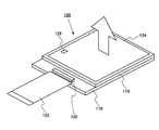
- FIG. 2 shows an aspect of the image display apparatus 100 according to an embodiment of the present invention.
- the image display device 100 includes a pixel portion 124 configured by arranging pixels 126, thereby providing an image display screen.
- a pixel 126 is provided on the element substrate 116 by an active element such as a light emitting element and a transistor, and an upper surface of the pixel portion 124 is covered with a sealing material 118.
- the element substrate 116 may be provided with a driver circuit 120 that outputs a signal for controlling the operation of the pixel 126.
- the element substrate 116 may be attached with a flexible printed wiring board 122 for connecting to an external circuit.
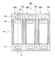
- FIG. 3 shows a configuration in which a first pixel 126a includes a first subpixel 127a, a second subpixel 128a, and a third subpixel 129a.
- the first subpixel 127a can be a subpixel corresponding to red
- the second subpixel 128a can be a subpixel corresponding to green
- the third subpixel 129a can be a subpixel corresponding to blue.
- Subpixels are not limited to those corresponding to these colors, but a single pixel may be configured by adding a subpixel corresponding to the intermediate color of the above-described colors or a subpixel corresponding to white. In this way, color display can be performed by configuring one pixel with a plurality of sub-pixels having different emission colors.
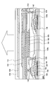
- FIG. 4 is a diagram for explaining a cross-sectional structure of a pixel.
- the cross-sectional structure of the pixel shown in FIG. 4 corresponds to the AB line shown in FIG. The following description will be given with reference to both FIG. 3 and FIG.
- the sub-pixel includes a light emitting element 102a and a first transistor 136.
- the light-emitting element 102a has the same structure as that described with reference to FIG. 1, and includes the first electrode 104, the first light-emitting layer 106, the second electrode 108, the second light-emitting layer 110, and the third electrode 112. Are stacked. That is, in the light-emitting element 102 a, the first light-emitting layer 106 is provided between the first electrode 104 and the second electrode 108, and the second electrode 108 is provided between the second electrode 108 and the third electrode 112. A light emitting layer 110 is provided.
- the first light emitting layer 106 and the second light emitting layer 110 are provided on substantially the entire surface of the pixel region. Since the first light-emitting layer 106 covers the first electrode 104, the first electrode 104 and the second electrode 108 are not in direct contact with each other. Similarly, since the second light-emitting layer 110 covers the second electrode 108, the second electrode 108 and the third electrode 112 are not in direct contact and short-circuited. Therefore, as shown in the plan view of FIG. 3, in each subpixel, the first electrode 104, the second electrode 108, and the third electrode 112 are provided so as to overlap each other, but the first electrode 104, the second electrode 108, and the third electrode 112 are overlapped with each other. The presence of the first light emitting layer 106 or the second light emitting layer 110 prevents the electrodes from being in direct contact with each other and causing a short circuit.
- the first electrode 104 is provided as an individual electrode for each subpixel, and is connected to the first transistor 136 at the first contact portion 130.
- the second electrode 108 is also provided as an individual electrode of each subpixel, and is connected to the wiring 140 that controls the potential in the second contact portion 132.
- the first light-emitting layer 106 is formed of an inorganic material as described above, the second electrode 108 formed on the upper surface of the first light-emitting layer 106 is finely formed using photolithography. There is no damage even if the machining process is applied.
- a bank layer 152 may be provided in the peripheral portion of the first electrode 104, and a step caused by the first electrode 104 may be reduced by the bank layer 152.
- the second electrode 108 can be used as a floating electrode without being connected to the wiring 140.
- the effective light emission area in the sub-pixel can be increased. That is, the aperture ratio of the pixel can be increased.
- the third electrode 112 is provided as a common electrode that applies a common potential to a plurality of subpixels. Therefore, the third electrode 112 is formed on substantially the entire surface of the second light emitting layer 110. Further, a sealing layer 154 is provided over the third electrode 112.
- the sealing layer 154 can be formed by combining a light-transmitting organic resin material, a light-transmitting inorganic insulating material, or a layer formed of an organic resin material and a layer formed of an inorganic material.
- the sealing layer 154 also functions as a protective layer, and can be provided on the third electrode 112 so that the light-emitting element 102a is not directly exposed to the air.
- FIG. 4 has a so-called top emission type pixel structure in which light emission of the first light emitting layer 106 and the second light emitting layer 110 is emitted from the third electrode 112 side. Therefore, the first electrode 104 is the above-described light reflective electrode, and the second electrode 108 and the third electrode 112 have a configuration of a light transmissive electrode.
- a region where the first electrode 104, the first light-emitting layer 106, the second electrode 108, the second light-emitting layer 110, and the third electrode 112 overlap is a light-emitting region.
- the first light-emitting layer 106 is a layer that emits light in the blue wavelength band
- the second light-emitting layer 110 is a layer that emits light in the yellow, red, and green emission wavelength bands.
- White light or light having a spectrum close to white light can be emitted from the 112 side.
- a color filter 156 can be provided over the light emitting region.
- the color filter 156 can be provided so as to be embedded in the sealing layer 154.
- the image display apparatus can perform color display.
- the color filters 156a, 156b, and 156c illustrated in FIG. 3 correspond to the first subpixel 127a, the second subpixel 128a, and the third subpixel 129a.
- the color filter 156 is manufactured by applying a colored layer that transmits light in a predetermined band and patterning the colored layer.
- the formation of the color filter is accompanied by the application of a chemical solution or a water washing treatment.
- a color filter can be provided above the light emitting layer. Accordingly, since a color filter can be formed on the element substrate 116 on which the light emitting element 102a is formed, the image display device can be reduced in thickness and weight.
- a plurality of light-emitting layers are provided in one subpixel so that light that can be regarded as white or pseudo white light is emitted, and a color filter is provided corresponding to each subpixel.
- the configuration of the light emitting element can be shared by the sub-pixels. That is, since it is not necessary to create a light emitting layer for each subpixel, the light emitting layer can be provided as a common layer for each subpixel. Therefore, the first light-emitting layer 106 and the second light-emitting layer 110 can be formed over substantially the entire pixel region. Further, by providing these light emitting layers over substantially the entire surface of the pixel region, a short circuit between the first electrode 104 and the second electrode 108 and a short circuit between the second electrode 108 and the third electrode 112 can be prevented. be able to.
- the second electrode 108 is formed on the first light-emitting layer 106 by dry etching or wet etching. Even if processed, the first light-emitting layer 106 is not damaged. For this reason, the subpixel can be miniaturized by a construction method using photolithography.
- An interlayer insulating layer is provided between the light-emitting element 102a and the first transistor 136.
- an interlayer insulating layer 142 is provided between the light-emitting element 102a and the first transistor 136.
- the interlayer insulating layer 142 may be formed of one layer or a plurality of layers.
- between the gate electrode 150 and the source / drain electrode 144, between the source / drain electrode 144 and the wiring 140, and The mode provided between the wiring 140 and the first electrode 104 is shown.
- the first electrode 104 of the light-emitting element 102 a is connected to the first transistor 136 at the first contact portion 130.
- the first contact portion 130 is provided with a contact hole that penetrates the interlayer insulating layer 142 and is electrically connected to the source / drain electrode 144 of the first transistor 136.
- Such a configuration in the first subpixel 127a is the same in the second subpixel 128a and the third subpixel 129a, and the first electrode of each subpixel is individually connected to the subpixel. The light emission is controlled.
- the first transistor 136 has a structure of a field effect transistor in which the semiconductor layer 146 and the gate electrode 150 are insulated by a gate insulating layer 148.
- the semiconductor layer 146 is formed using amorphous or polycrystalline silicon or an oxide semiconductor, and when a gate voltage is applied to the gate electrode 150, a channel is formed in the semiconductor layer 146. It has the form of a thin film transistor.
- a light emitting element having a plurality of light emitting layers using quantum dots and a transistor can be provided on the same substrate.
- the image display device can be thinned and miniaturized.
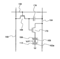
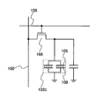
- 5A and 5B are circuit diagrams illustrating an example of a circuit configuration of a pixel including the light emitting element 102a and the transistor as illustrated in FIG.
- FIG. 5A shows a first selection transistor 166 that performs a switching operation by a scanning signal applied to the scanning signal line 158, and a video signal applied from the first video signal line 160 when the first selection transistor 166 is turned on.
- An example of a pixel circuit including a first driving transistor 170 to which a potential based on the gate is supplied and a light-emitting element 102a connected to the first driving transistor 170 is shown.
- the first driving transistor 170 is connected between the power supply line 164 and the light emitting element 102a.
- the first driving transistor 170 illustrated in FIG. 5A corresponds to the first transistor 136 illustrated in FIG.
- FIG. 5A shows an equivalent circuit of a pixel. 5A, the structure of the light-emitting element 102a will be described with reference to FIG. 4.
- the first electrode 104 is connected to the first driving transistor 170, and a common potential is applied to the third electrode 112.
- the second electrode 108 between the first electrode 104 and the third electrode 112 may be given a predetermined control potential (Vc) or may be a floating potential.
- the light-emitting element 102a is sandwiched between the first capacitor 104 formed by the first light-emitting layer 106 sandwiched between the first electrode 104 and the second electrode 108, and the second electrode 108 and the third electrode. It can also be regarded as a capacitive element in which the second capacitor portion of the second light emitting layer 110 is connected in series.
- Vc control potential
- the electric field strength applied to the first light-emitting layer 106 and the second light-emitting layer 110 is controlled by the control potential (Vc).
- the emission intensity can be adjusted accordingly.
- the second electrode 108 is set to a floating potential, when a video signal is supplied to the subpixel, the second electrode 108 can function as a memory that holds a predetermined potential corresponding to the video signal.
- FIG. 5B shows a first selection transistor 166 that performs a switching operation according to a scanning signal applied to the scanning signal line 158, and a potential corresponding to the video signal from the first video signal line 160 via the first selection transistor 166.
- An example of a pixel circuit in which the light-emitting element 102 a emits light with the charge given to the first capacitor 174 and accumulated in the first capacitor 174 is shown.
- the first selection transistor 166 illustrated in FIG. 5B corresponds to the first transistor 136 illustrated in FIG.
- the first electrode 104 of the light-emitting element 102 a is connected to the first selection transistor 166 and the first capacitor 174, and a common potential is applied to the third electrode 112.
- the potential of the second electrode 108 is similar to that in the case of FIG. 5A and can be a control potential (Vc) or a floating potential.
- the number of transistors constituting the pixel may be one, and in the case of top emission, the area of the capacitor can be increased without affecting the aperture ratio of the pixel.
- the charge accumulated in the element 174 can cause the light-emitting element 102a to emit light with sufficient light emission intensity.
- the light emitting layer can be stacked with an intermediate electrode interposed therebetween.
- the second electrode corresponding to the intermediate electrode can be an individual electrode in each sub-pixel. Therefore, a plurality of light-emitting layers are formed between the first electrode and the second electrode using quantum dots, and a second electrode is separately provided between the light-emitting layers, so that each light-emitting layer is applied.
- the light emission intensity can be adjusted by controlling the electric field intensity.
- a white light emitting element can be obtained by stacking a plurality of light emitting layers having different emission wavelength bands using quantum dots, color display can be performed by providing a color filter on the light emitting surface. it can. For this reason, it is not necessary to pattern a light emitting layer for every pixel (each subpixel), and simplification of a process becomes easy.
- FIG. 6 shows a mode in which one pixel 126b is composed of a first subpixel 127b, a second subpixel 128b, and a third subpixel 129b.
- the first subpixel 127b can be a subpixel corresponding to red
- the second subpixel 128b can be a subpixel corresponding to green
- the third subpixel 129b can be a subpixel corresponding to blue.
- Subpixels are not limited to those corresponding to these colors, but a single pixel may be configured by adding a subpixel corresponding to the intermediate color of the above-described colors or a subpixel corresponding to white. In this way, color display can be performed by configuring one pixel with a plurality of sub-pixels having different emission colors.
- the first subpixel 127b is provided with the first electrode 104, the second electrode 108, and the third electrode 112.
- the first electrode 104, the second electrode 108, and the third electrode 112 are provided as individual electrodes belonging to the first subpixel 127b.
- This electrode configuration is the same for the second subpixel 128b and the third subpixel 129b. That is, the difference from the pixel configuration in the first embodiment is that the third electrode 112 is not an electrode common to each pixel but is provided individually corresponding to each sub-pixel.
- FIG. 7 is a diagram for explaining a cross-sectional structure of a pixel.
- the cross-sectional structure of the pixel shown in FIG. 7 corresponds to the CD line shown in FIG. The following description will be given with reference to both FIG. 6 and FIG.
- a light-emitting element 102b includes a first light-emitting layer, a first electrode 104, a second electrode 108, a third electrode 112, a first light-emitting layer 106, and a second light-emitting layer 110.
- 106 is sandwiched between the first electrode 104 and the second electrode 108
- the second light emitting layer 110 is sandwiched between the second electrode 108 and the third electrode 112
- the first electrode 104 is The point connected to the first transistor 136 is the same as in the first embodiment.
- the third electrode 112 is connected to the second transistor 138 at the third contact portion 134.
- the second transistor 138 has the same structure as the first transistor 136.
- the third contact portion 134 has a contact hole that penetrates the first light emitting layer 106, the second light emitting layer 110, the bank layer 152, and the interlayer insulating layer 142.
- the third electrode 112 is provided on the upper surface of the second light emitting layer 110, and is electrically connected to the source / drain electrode 144 b of the second transistor 138 through the contact hole in the third contact portion 134.
- first light emitting layer 106 and the second light emitting layer 110 are formed of an inorganic semiconductor material including quantum dots
- contact holes can be formed by dry etching or wet etching. Then, the third electrode 112 of each subpixel is connected to the second transistor 138, whereby the potential of the third electrode 112 is made different for each subpixel and the luminance and hue of the light emitting element 102b are controlled. be able to.
- FIG. 8 shows an example of a circuit configuration of a pixel that can be constituted by the sub-pixel having the configuration shown in FIG.
- the connection relationship between the first selection transistor 166, the first driving transistor 170, the first capacitor 174, and the light-emitting element 102b is the same as that of the circuit illustrated in FIG. 5A.
- the second selection transistor 168, the second driving transistor 172, and the second capacitor element 176 are provided in order to control the potential of the third electrode 112 of the light emitting element 102b.
- the second selection transistor 168 has a gate connected to the scanning signal line 158 and an input terminal connected to the second video signal line 162.
- the output-side terminal of the second selection transistor 168 is connected to the gate of the second drive transistor 172, and a potential based on the video signal applied to the second video signal line 162 is applied to the gate of the second drive transistor 172. It is done.
- the second capacitor element 176 has a function of being charged with the gate potential and holding the gate potential.
- the second electrode 108 of the light emitting element 102b is connected to the wiring 140.
- a certain potential is applied to the wiring 140.
- the potential of the wiring 140 may be a potential commonly applied to the light emitting elements of the sub-pixels, and may be, for example, a ground potential or a low level reference potential. Since the second electrode 108 is connected to the wiring 140 to which a constant common potential is applied, the video signals applied to the first video signal line 160 and the second video signal line 162 can be made different. That is, the potential of the first electrode 104 and the potential of the third electrode 112 in the light-emitting element 102b can be different. Accordingly, the light emission intensity of the first light-emitting layer 106 and the light emission intensity of the second light-emitting layer 110 can be made different.
- the emission spectrum of the first light-emitting layer 106 and the emission spectrum of the second light-emitting layer 110 are different, the light intensity emitted from the light-emitting element 102b can be controlled by individually controlling the emission intensity of both.
- the composite spectrum can be changed.
- the light emission intensities of the first light-emitting layer and the second light-emitting layer are individually changed by individually controlling the potentials of the first electrode and the third electrode of the light-emitting element. be able to. Thereby, the color tone of the light emitted from the light emitting element can be adjusted.
- the image display apparatus according to this embodiment is the same as that of the first embodiment except that the potential of the third electrode can be independently controlled. Therefore, this embodiment is also the first embodiment. The same effect can be obtained.
- the present embodiment shows one mode of a light-emitting element having a configuration in which a plurality of light-emitting layers are arranged in a horizontal direction (horizontal direction) and an image display device in which pixels are configured by the light-emitting elements.
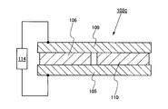
- FIG. 9 shows a configuration of the light emitting element 102c constituting the pixel of the image display device according to the embodiment of the present invention.
- the light emitting element 102c has a plurality of light emitting layers, and these are provided between a pair of electrodes. That is, as shown in FIG. 9, the first light-emitting layer 106 and the second light-emitting layer 110 are juxtaposed and are sandwiched between the first electrode 105 and the second electrode 109. Since the first light-emitting layer 106 and the second light-emitting layer 110 are juxtaposed and sandwiched between the first electrode 105 and the second electrode 109, it is considered that two light-emitting cells are connected in parallel. You can also.
- the first electrode 105 and the second electrode 109 are connected to the driving power source 114 to give a potential difference, whereby the same potential difference is applied to the first light emitting layer 106 and the second light emitting layer 110.
- the first light-emitting layer 106 and the second light-emitting layer 110 emit light when a predetermined potential difference is applied. Note that the configurations of the first light-emitting layer 106 and the second light-emitting layer 110 are the same as those described in the first embodiment.
- the first light-emitting layer 106 is blue light emission whose emission wavelength peak position is 435 nm to 480 nm
- the second light emission layer 110 is yellow light emission whose emission wavelength peak position is 580 nm to 595 nm, or 500 nm to 560 nm.
- the emitted light from the light emitting element 102c can be white light or apparently white light.
- the light emission spectra of the first light emitting layer 106 and the second light emitting layer 110 are different from each other, in a situation where the light emitting element 102c can be regarded as a point light source, the light emission of each light emitting layer is possible even when the light emitting layers are arranged in parallel. It is possible to ignore the influence of color separation that is visually recognized when colors are separated.
- the first light-emitting layer 106 and the second light-emitting layer 110 do not need to have the same film thickness and may be different.
- each light emitting layer can be emitted through the electrode on the light emitting surface. That is, when the light emitting layers are stacked in the vertical direction, the light emission of the light emitting layer located on the lower layer side may be absorbed and attenuated by the upper light emitting layer, but according to the light emitting element 102c of this embodiment. Such a problem can be solved.
- the light emission direction of the light emitting element 102c can be determined by the configuration of the electrodes. For example, in the light-emitting element 102c, when the second electrode 109 is a light-transmitting electrode and the first electrode 105 is a light-reflective electrode, the second electrode 109 from the side of the second electrode 109 that is a light-transmitting electrode is used. Light emitted from the first light emitting layer 106 and the second light emitting layer 110 can be emitted.
- the light-emitting layer is not limited to two layers, and includes three layers including a light-emitting layer corresponding to blue light, a light-emitting layer corresponding to green light, and a light-emitting layer corresponding to red light, and each of the light emitting layers is similar to the structure shown in FIG.
- the light emitting layer may be sandwiched between electrodes and arranged side by side so that white light or light having a spectrum close to white light is emitted from the light emitting element.
- the color balance can be adjusted by the area of the light emitting layer.
- the area of the first light-emitting layer 106 that emits blue light with low visibility may be made larger than the area of the second light-emitting layer 110.
- the color balance of the emitted light of the light emitting element 102c can be adjusted by increasing the area of the light emitting layer having low current efficiency with respect to light emission luminance as compared with the area of the light emitting layer having relatively high current efficiency. .
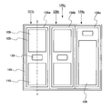
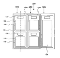
- FIG. 10 shows a configuration in which a single pixel 126c includes a first subpixel 127c, a second subpixel 128c, and a third subpixel 129c.
- the first subpixel 127c can be a subpixel corresponding to red
- the second subpixel 128c can be a subpixel corresponding to green
- the third subpixel 129c can be a subpixel corresponding to blue.
- Subpixels are not limited to those corresponding to these colors, but a single pixel may be configured by adding a subpixel corresponding to the intermediate color of the above-described colors or a subpixel corresponding to white.
- the pixel 126c shown in FIG. 10 is basically a combination of a light emitting element that emits white light and a color filter, but the color filter 156c may not be provided for the third subpixel 129c corresponding to blue. Good. That is, in the third subpixel 129c, if the first light emitting layer 106 emits blue light, the second light emitting layer 110 that emits yellow light having a complementary color relationship is omitted. be able to. According to this embodiment, since the first light-emitting layer 106 is provided using quantum dots, the half-value width of the emission spectrum is narrow and blue light emission with high color purity is possible, so even without using a color filter. Color purity does not decrease.
- the light emitting efficiency of the first light emitting layer 106 that emits light in the wavelength band corresponding to blue is low, light emitted from the light emitting layer can be prevented from being absorbed and attenuated by the color filter. Effective use of light can be achieved. Accordingly, the light emission intensity of the first light-emitting layer 106 in the third subpixel 129c can be reduced, and deterioration of the light-emitting element can be suppressed.
- FIG. 10 illustrates a mode in which the first light-emitting layer 106 and the second light-emitting layer 110 are juxtaposed, but the arrangement and arrangement of the light-emitting layers are not limited thereto.
- the light emitting layer may be divided into a plurality of patterns, and the island-shaped regions of the first light emitting layer 106 and the second light emitting layer 110 may be alternately arranged.
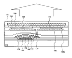
- FIG. 11 shows a cross-sectional structure of such a pixel.
- the cross-sectional structure of the pixel shown in FIG. 11 corresponds to the EF line shown in FIG.
- the light emitting element 102c is connected to the first transistor 136 by the first contact portion 130.
- the first light-emitting layer 106 and the second light-emitting layer 110 are juxtaposed on the first electrode 105.
- Such an arrangement of the light emitting layers can be realized by sequentially forming the first light emitting layer 106 and the second light emitting layer 110 after forming the first electrode 105.
- the light emitting layer is formed of an inorganic material using quantum dots, for example, a fine pattern can be formed by mask formation by photolithography and processing by etching. Thus, a fine light-emitting layer pattern can be formed on one subpixel (on the first electrode 105).
- a second electrode 109 is provided on the light emitting and emitting layer, and the whole surface is covered with a sealing layer 154.
- the color filter 156 By providing the color filter 156 on the light emission surface, light in a predetermined wavelength band can be output as the emitted light. Even when the color filter 156 is provided, the first light-emitting layer 106 and the second light-emitting layer 110 are formed using quantum dots that are inorganic materials, so that the light-emitting layer is not damaged.
- the color filter 156 can be provided on the element substrate 116 on which the light emitting element 102c is formed, the image display apparatus can be reduced in thickness and weight.
- a plurality of light emitting layers using quantum dots can be juxtaposed on the electrode.
- the plurality of light-emitting layers provided over the first electrode can form sub-pixels that emit light that can be regarded as white or pseudo white by changing the emission spectrum.
- the chromaticity can be adjusted by changing the area of each light emitting layer.
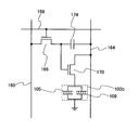
- 12A and 12B are circuit diagrams illustrating an example of a circuit configuration of a pixel including a light emitting element 102c and a transistor as illustrated in FIG.
- the connection relationship between the first selection transistor 166, the first driving transistor 170, the first capacitor 174, and the light-emitting element 102c is the same as that of the circuit illustrated in FIG. 5A.
- the light-emitting element 102 c has a relationship in which the first light-emitting layer 106 and the second light-emitting layer 110 are connected in parallel to the first driving transistor 170. Therefore, the drain current of the driving transistor flows in a diverted manner according to the characteristics of the first light emitting layer 106 and the second light emitting layer 110.
- the connection relationship between the first selection transistor 166, the first capacitor 174, and the light-emitting element 102c is the same as that of the circuit illustrated in FIG. 5B.
- the first electrode 105 of the light-emitting element 102c is connected to the first selection transistor 166 and the first capacitor 174, and a common potential is applied to the second electrode 109, so that the first capacitor 105 has a common potential.
- a higher predetermined potential is applied, electric charge is supplied from the first capacitor 174 to the light-emitting element 102c to emit light.
- a plurality of light emitting layers can be arranged in parallel on the same electrode by forming the light emitting layer using quantum dots.
- the color tone can be adjusted by making the area ratios of the plurality of light emitting layers different.
- a light-emitting element that emits white light can be obtained by combining a plurality of light-emitting layers having different emission wavelengths, an image display device that performs color display by providing a color filter on a light-emitting surface of a pixel is provided. Can be realized.
- a plurality of light emitting layers are arranged in a horizontal direction (horizontal direction), and a light emitting element having a configuration capable of individually controlling light emission by each light emitting layer, and an image display in which pixels are configured by the light emitting elements.
- a light emitting element having a configuration capable of individually controlling light emission by each light emitting layer, and an image display in which pixels are configured by the light emitting elements.
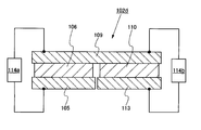
- FIG. 13 shows a configuration of a light emitting element 102d that constitutes a pixel of an image display device according to an embodiment of the present invention.
- the first light-emitting layer 106 is provided between the first electrode 105 and the second electrode 109
- the second light-emitting layer 110 is formed between the third electrode 113 and the second electrode 109. It is provided in between. That is, the light-emitting element 102 d has the second electrode 109 in common, the first electrode 105 corresponds to the first light-emitting layer 106, and the third electrode 113 corresponds to the second light-emitting layer 110. ing.
- the light emitting element 102d according to the present embodiment is related to the third embodiment in that one of the electrodes sandwiching the plurality of light emitting layers juxtaposed is divided and provided corresponding to each light emitting layer. It is different from the light emitting element. Due to this difference, in the light-emitting element 102d illustrated in FIG. 13, the first light-emitting layer 106 and the second light-emitting layer 110 can be individually controlled to emit light.
- the first electrode 105 and the second electrode 109 sandwiching the first light emitting layer 106 are connected to the first driving power supply 114a, and the third electrode 113 and the second electrode sandwiching the second light emitting layer 110 are connected.
- the electrode 109 is connected to the second drive power supply 114b.
- the light emitting element 102d can emit light by changing the driving voltages of the first driving power supply 114a and the second driving power supply 114b.
- one light-emitting layer of the light-emitting element 102d can be in a non-light-emitting state and light can be emitted only from the other light-emitting layer.
- the structure of the 1st light emitting layer 106 and the 2nd light emitting layer 110 is the same as that of what is demonstrated in 1st Embodiment. That is, the first light-emitting layer 106 is blue light emission whose emission wavelength peak position is 435 nm to 480 nm, and the second light emission layer 110 is yellow light emission whose emission wavelength peak position is 580 nm to 595 nm, or 500 nm to 560 nm. With green light emission and red light emission of 610 nm to 750 nm, the emitted light from the light emitting element 102d can be white light or apparently white light.
- the light-emitting layer is not limited to these combinations, and three layers of a light-emitting layer corresponding to blue light, a light-emitting layer corresponding to green light, and a light-emitting layer corresponding to red light may be provided.
- the light emission direction of the light emitting element 102d can be determined by the configuration of the electrodes.
- the second electrode 109 is a light-transmitting electrode and the first electrode 105 and the third electrode 113 are light-reflecting electrodes
- the second light-transmitting electrode is used.
- the light emitted from the first light-emitting layer 106 and the second light-emitting layer 110 can be emitted from the electrode 109 side.
- the areas of the first light emitting layer 106 and the second light emitting layer 110 can be made different from those in the third embodiment. The balance can be adjusted.
- FIG. 14 shows a configuration in which the first sub-pixel 127d, the second sub-pixel 128d, and the third sub-pixel 129d are included in one pixel 126d as in the third embodiment. Further, the third sub-pixel 129d corresponding to blue has a configuration in which no color filter is provided.
- FIG. 15 shows a cross-sectional structure of such a pixel.
- the cross-sectional structure of the pixel shown in FIG. 15 corresponds to the line EF shown in FIG.
- the first electrode 105 is connected to the first transistor 136 at the first contact portion 130, and the third electrode 113 is connected to the second contact portion 132 in the second contact portion 132.
- the transistor 138 is connected. Since the second electrode 109 is supplied with a common potential (eg, ground potential), it is applied to the first light-emitting layer 106 and the second light-emitting layer 110 by the first transistor 136 and the second transistor 138. Light can be emitted with different potentials.
- a common potential eg, ground potential
- the first electrode 105 and the third electrode 113 are light reflective electrodes
- the second electrode 109 is a light transmissive electrode. Therefore, the second electrode 109 serves as a light emission surface, and by providing the color filter 156 on the upper surface side, light in a specific band can be used as emission light of the subpixel. In this case, if one sub-pixel can be regarded as a point light source, even if a plurality of light-emitting layers having different wavelength bands of emitted light are juxtaposed, the influence of color separation that is visible when the emitted color is separated is ignored. be able to.
- a plurality of light emitting layers using quantum dots are juxtaposed, and light emission is individually controlled to form a sub-pixel that emits light that can be regarded as white or pseudo white. Can do.
- the chromaticity can be adjusted by changing the potential applied to each light emitting layer.
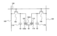
- 16A and 16B are circuit diagrams illustrating an example of a circuit configuration of a pixel including the light-emitting element 102d and the transistor illustrated in FIG.
- connection relationship between the first selection transistor 166, the first driving transistor 170, the first capacitor 174, and the light-emitting element 102d is the same as that of the circuit illustrated in FIG. 5A.
- the connection relationship between the second selection transistor 168, the second driving transistor 172, the second capacitor 176, and the light-emitting element 102d is also the same. However, the difference is that the first driving transistor 170 is connected to the first electrode 105 of the light emitting element 102 d and the second driving transistor 172 is connected to the third electrode 113.
- the first selection transistor 166 is connected to the first video signal line 160
- the second selection transistor 168 is connected to the second video signal line 162
- the first driving transistor 170 and the second driving transistor are connected. Both are connected to the power supply line 164.
- the potential applied to the first electrode 105 flows through the first light-emitting layer 106.
- Current and the potential applied to the third electrode 113 (current flowing through the second light-emitting layer 110) can be individually controlled.
- FIG. 5B This is the same as the circuit shown in FIG.
- the first electrode 105 of the light-emitting element 102d is connected to the first selection transistor 166 and the first capacitor 174, and the third electrode 113 is connected to the second selection transistor 168 and the second capacitor 176. Then, a common potential is applied to the second electrode 109. Accordingly, when a predetermined potential higher than the common potential is applied to the first capacitor 174, the first light-emitting layer 106 can emit light due to a potential difference between the first electrode 105 and the second electrode 109. The same applies to the second light emitting layer 110.
- a plurality of light emitting layers can be arranged in parallel on the same electrode by forming the light emitting layer using quantum dots. And by providing an individual electrode corresponding to each light emitting layer, light emission of each light emitting layer can be controlled. In this case, the light emission intensity of each light emitting layer can be controlled by the potential applied to the individual electrode, whereby the light emission intensity can be changed and the color tone can be adjusted.
- a light-emitting element that emits white light can be obtained by combining a plurality of light-emitting layers having different emission wavelengths
- an image display device that performs color display by providing a color filter on a light-emitting surface of a pixel is provided. Can be realized.
- the light emission intensity corresponding to the individual electrode can be adjusted by fixing the potential applied to the individual electrode and controlling the length of the light emission time using an appropriate circuit. .
- DESCRIPTION OF SYMBOLS 100 ... Image display apparatus, 102 ... Light emitting element, 104 ... 1st electrode, 105 ... 1st electrode, 106 ... 1st light emitting layer, 108 ... 2nd Electrode 109 ... second electrode 110 ... second light emitting layer 112 ... third electrode 113 ... third electrode 114 ... drive power source 116 ... Element substrate 118 ... Sealing material 120 ... Driver circuit 122 ... Flexible printed circuit board 124 ... Pixel part 126 ... Pixel 127 ... First sub-pixel 128 ... 2nd subpixel, 129 ... 3rd subpixel, 130 ... 1st contact part, 132 ... 2nd contact part, 134 ...
- 3rd contact part 136: first transistor, 138: second transistor, 140: arrangement 142 ... interlayer insulation layer, 144 ... source / drain electrodes, 146 ... semiconductor layer, 148 ... gate insulation layer, 150 ... gate electrode, 152 ... bank layer, 154 ... Sealing layer, 156... Color filter, 158..., Scanning signal line, 160 ... first video signal line, 162 ... second video signal line, 164 ... power supply line, 166 ... 1st selection transistor, 168 ... 2nd selection transistor, 170 ... 1st drive transistor, 172 ... 2nd drive transistor, 174 ... 1st capacitive element, 176 ... Second capacitor element
Landscapes
- Engineering & Computer Science (AREA)
- Physics & Mathematics (AREA)
- General Physics & Mathematics (AREA)
- Theoretical Computer Science (AREA)
- Computer Hardware Design (AREA)
- Microelectronics & Electronic Packaging (AREA)
- Geometry (AREA)
- Chemical & Material Sciences (AREA)
- Crystallography & Structural Chemistry (AREA)
- Inorganic Chemistry (AREA)
- Nanotechnology (AREA)
- Optics & Photonics (AREA)
- Electroluminescent Light Sources (AREA)
- Devices For Indicating Variable Information By Combining Individual Elements (AREA)
Abstract
Description
本実施形態は、複数の発光層を縦方向(垂直方向)に積層した構成を有する発光素子及び当該発光素子で画素を構成した画像表示装置の一態様について示す。
図1は、本発明の一実施形態に係る画像表示装置の画素を構成する発光素子102aの構成を示す。発光素子102aは、複数の発光層が設けられている。複数の発光層のそれぞれは、電極に挟まれている。図1で示す発光素子102aは、3つの電極によって2つの発光層が挟まれた構造を有している。具体的には、発光素子102aは、第1の発光層106が第1の電極104と第2の電極108に挟まれ、第2の発光層110が第2の電極108と第3の電極112に挟まれた構造を有している。第1の発光層106と第2の発光層110とは第2の電極108を挟んで積層されているので、第2の電極108は上下にある2つの発光層で共有されているとみなすこともできる。
図2は、本発明の一実施形態に係る画像表示装置100の一態様を示す。画像表示装置100は、画素126が配列して構成される画素部124を有し、これによって画像表示画面が設けられている。素子基板116には、発光素子及びトランジスタなどによる能動素子によって画素126が設けられており、画素部124の上面が封止材118によって覆われている。素子基板116には、画素126の動作を制御する信号を出力するドライバ回路120が設けられていてもよい。また、素子基板116には、外部回路と接続するためのフレキシブルプリント配線基板122が取り付けられていてもよい。
図3及び図4を参照して、本実施形態に係る画像表示装置の画素部の構成を示す。なお、本実施形態において画素は複数の副画素によって構成されているものとする。
本実施形態は、第1の実施形態で説明した副画素において、第3の電極も副画素ごとに電位を制御することのできる構成について、図6及び図7を参照して説明する。
図6は、一つ画素126bが、第1の副画素127b、第2の副画素128b、第3の副画素129bにより構成されている態様を示す。例えば、第1の副画素127bを赤色に対応する副画素、第2の副画素128bを緑色に対応する副画素、第3の副画素129bを青色に対応する副画素とすることができる。副画素はこれらの色に対応するものだけでなく、前述する色の中間色に対応する副画素や、白色に対応する副画素を追加が追加されて一つの画素が構成されてもよい。このように一つの画素を発光色の異なる複数の副画素で構成することによりカラー表示をすることができる。
本実施形態は、複数の発光層を横方向(水平方向)に配置した構成を有する発光素子及び当該発光素子で画素を構成した画像表示装置の一態様について示す。
図9は、本発明の一実施形態に係る画像表示装置の画素を構成する発光素子102cの構成を示す。発光素子102cは、複数の発光層を有し、これらが一対の電極間に設けられている。すなわち、図9で示すように、第1の発光層106と第2の発光層110は並置され、共に第1の電極105と第2の電極109に挟まれている。第1の発光層106と第2の発光層110とは並置され、共に第1の電極105と第2の電極109によって挟まれているので、2つの発光セルが並列に接続されているとみなすこともできる。
図10及び図11を参照して、本実施形態に係る画像表示装置の画素部の構成を示す。本実施形態も、他の実施形態と同様に、画素は複数の副画素によって構成されているものとする。
本実施形態は、複数の発光層を横方向(水平方向)に配置すると共に、各発光層による発光を個別に制御することができる構成を有する発光素子及び当該発光素子で画素を構成した画像表示装置の一態様について示す。
図13は、本発明の一実施形態に係る画像表示装置の画素を構成する発光素子102dの構成を示す。発光素子102dは、第1の発光層106が第1の電極105と第2の電極109との間に設けられ、第2の発光層110が第3の電極113と第2の電極109との間に設けられている。すなわち、発光素子102dは、第2の電極109を共通とし、第1の電極105が第1の発光層106に対応し、第3の電極113が第2の発光層110に対応して設けられている。
図14及び図15を参照して、本実施形態に係る画像表示装置の画素部の構成を示す。本実施形態も、他の実施形態と同様に、画素は複数の副画素によって構成されているものとする。
Claims (20)
- 複数の副画素で一つの画素が構成され前記画素が2次元に配列した画素領域を有し、
前記副画素は電極を挟んで重畳するように設けられた複数の発光層を含み、
前記複数の発光層は、それぞれが量子ドット材料を含んで構成され、かつ発光波長のピーク位置が互いに異なることを特徴とする画像表示装置。 - 前記副画素は、第1の電極と第2の電極との間に設けられた第1の発光層と、第2の電極と、前記第2の電極の前記第1の電極とは反対の側に位置する第3の電極との間に設けられた第2の発光層と、を有することを特徴とする請求項1に記載の画像表示装置。
- 前記第1の発光層は発光波長のピークが435nm~480nmにあり、前記第2の発光層は発光波長のピークが580nm~595nmにある黄色発光、または500nm~560nmの緑色発光及び610nm~750nmにあることを特徴とする請求項2に記載の画像表示装置。
- 前記第1の電極は、第1のトランジスタのソース・ドレイン電極に接続し、
前記第3の電極は、前記複数の副画素に跨って配置され、共通電位が印加されていることを特徴とする請求項2に記載の画像表示装置。 - 前記第1の電極は、第1のトランジスタのソース・ドレイン電極に接続し、
前記第3の電極は、第2のトランジスタのソース・ドレイン電極に接続し、
前記第1のトランジスタのゲート電極には、第1の映像信号線から供給される第1の映像信号が入力され、
前記第2のトランジスタのゲート電極には、第2の映像信号線から供給される第2の映像信号が入力されることを特徴とする請求項2に記載の画像表示装置。 - 前記発光層の上方にカラーフィルタが設けられていることを特徴とする請求項1に記載の画像表示装置。
- 前記第1の電極は光反射面を有し、前記第2の電極及び前記第3の電極は透光性を有することを特徴とする請求項2に記載の画像表示装置。
- 前記発光層が前記画素領域の略全面に設けられていることを特徴とする請求項1に記載の画像表示装置。
- 前記第1の電極、前記第2の電極及び前記第3の電極のぞれぞれは、個別に電位が制御されることを特徴とする請求項2に記載の画像表示装置。
- 前記第1の電極及び前記第3の電極は個別に電位が制御され、前記第2の電極はフローティング電位であることを特徴とする請求項2に記載の画像表示装置。
- 複数の副画素で一つの画素が構成され、前記画素が2次元に配列した画素領域を有し、
前記複数の副画素の少なくとも一つは、複数の発光層が並置されており、
前記複数の発光層は、それぞれが量子ドット材料を含んで構成され、かつ発光波長のピーク位置が互いに異なることを特徴とする画像表示装置。 - 前記画素は、赤色に対応する第1の副画素と、緑色に対応する第2の副画素と、青色に対応する第3の副画素を含み、
前記第1の副画素と前記第2の副画素は前記発光層の上方にカラーフィルタが設けられ、
前記第3の副画素にはカラーフィルタが設けられていないことを特徴とする請求項11に記載の画像表示装置。 - 前記複数の副画素は、前記複数の発光層が並置されている第1の副画素と、量子ドット材料を含む発光層を1つ備えた第2の副画素とを含むことを特徴とする請求項11に記載の画像表示装置。
- 前記第2の副画素は、青色の発光をし、且つカラーフィルタが設けられていないことを特徴とする請求項13に記載の画像表示装置。
- 前記副画素は、第1の電極と第2の電極との間に、第1の発光層及び第2の発光層が並置され、
前記第1の電極は、第1のトランジスタのソース・ドレイン電極に接続し、
前記第2の電極は、前記複数の副画素に跨って配置され、共通電位が印加されていることを特徴とする請求項11に記載の画像表示装置。 - 前記第1の電極は光反射面を有し、前記第2の電極は透光性を有することを特徴とする請求項15に記載の画像表示装置。
- 前記副画素は、第1の電極と第2の電極との間に設けられた第1の発光層と、第3の電極と前記第2の電極との間に設けられた第2の発光層とを有することを特徴とする請求項11に記載の画像表示装置。
- 前記第1の電極及び前記第3の電極は光反射面を有し、前記第2の電極は透光性を有することを特徴とする請求項17に記載の画像表示装置。
- 前記第1の電極、前記第2の電極及び前記第3の電極のぞれぞれは、個別に電位が制御されることを特徴とする請求項17に記載の画像表示装置。
- 前記第1の電極は、第1のトランジスタのソース・ドレイン電極に接続し、
前記第3の電極は、第2のトランジスタのソース・ドレイン電極に接続し、
前記第1のトランジスタのゲート電極には、第1の映像信号線から供給される第1の映像信号が入力され、
前記第2のトランジスタのゲート電極には、第2の映像信号線から供給される第2の映像信号が入力されることを特徴とする請求項17に記載の画像表示装置。
Priority Applications (3)
| Application Number | Priority Date | Filing Date | Title |
|---|---|---|---|
| KR1020177005900A KR20170038061A (ko) | 2014-10-03 | 2015-08-21 | 화상 표시 장치 |
| CN201580047219.XA CN107079559B (zh) | 2014-10-03 | 2015-08-21 | 图像显示装置 |
| US15/514,159 US10510801B2 (en) | 2014-10-03 | 2015-08-21 | Image display device with quantum dot |
Applications Claiming Priority (2)
| Application Number | Priority Date | Filing Date | Title |
|---|---|---|---|
| JP2014204627A JP6391401B2 (ja) | 2014-10-03 | 2014-10-03 | 画像表示装置 |
| JP2014-204627 | 2014-10-03 |
Publications (1)
| Publication Number | Publication Date |
|---|---|
| WO2016051992A1 true WO2016051992A1 (ja) | 2016-04-07 |
Family
ID=55630038
Family Applications (1)
| Application Number | Title | Priority Date | Filing Date |
|---|---|---|---|
| PCT/JP2015/073558 Ceased WO2016051992A1 (ja) | 2014-10-03 | 2015-08-21 | 画像表示装置 |
Country Status (5)
| Country | Link |
|---|---|
| US (1) | US10510801B2 (ja) |
| JP (1) | JP6391401B2 (ja) |
| KR (1) | KR20170038061A (ja) |
| CN (1) | CN107079559B (ja) |
| WO (1) | WO2016051992A1 (ja) |
Cited By (5)
| Publication number | Priority date | Publication date | Assignee | Title |
|---|---|---|---|---|
| WO2019174290A1 (zh) * | 2018-03-16 | 2019-09-19 | 京东方科技集团股份有限公司 | 阵列基板、其制造方法、以及显示装置 |
| WO2020049738A1 (ja) * | 2018-09-07 | 2020-03-12 | シャープ株式会社 | 表示デバイス |
| CN112567446A (zh) * | 2018-08-21 | 2021-03-26 | 株式会社半导体能源研究所 | 显示装置及电子设备 |
| WO2022126562A1 (zh) * | 2020-12-17 | 2022-06-23 | 京东方科技集团股份有限公司 | 量子点发光器件、显示装置和制作方法 |
| WO2024053088A1 (ja) * | 2022-09-09 | 2024-03-14 | シャープディスプレイテクノロジー株式会社 | 発光素子および表示装置 |
Families Citing this family (27)
| Publication number | Priority date | Publication date | Assignee | Title |
|---|---|---|---|---|
| JP2017026815A (ja) * | 2015-07-22 | 2017-02-02 | 株式会社ジャパンディスプレイ | 表示装置 |
| US20200098957A1 (en) * | 2017-01-18 | 2020-03-26 | Cree Huizhou Solid State Lighting Company Ltd. | Multiple led light source lens design in an integrated package |
| JP7059574B2 (ja) * | 2017-02-01 | 2022-04-26 | セイコーエプソン株式会社 | 電気光学装置、電子機器、ヘッドマウントディスプレイ |
| KR102560918B1 (ko) * | 2017-12-29 | 2023-07-27 | 엘지디스플레이 주식회사 | 전계 발광 표시장치 |
| US11737301B2 (en) | 2018-03-19 | 2023-08-22 | Samsung Electronics Co., Ltd. | Electroluminescent device, and display device comprising thereof |
| US11005060B2 (en) * | 2018-03-19 | 2021-05-11 | Samsung Electronics Co., Ltd. | Electroluminescent device, and display device comprising thereof |
| CN108630733B (zh) | 2018-05-07 | 2020-12-25 | 京东方科技集团股份有限公司 | 一种显示面板 |
| CN109585504B (zh) * | 2018-10-08 | 2020-12-25 | 惠科股份有限公司 | 显示面板及显示面板的制作方法 |
| KR102589861B1 (ko) * | 2018-11-01 | 2023-10-16 | 삼성전자주식회사 | 표시 장치 |
| KR102649218B1 (ko) * | 2018-11-15 | 2024-03-19 | 삼성디스플레이 주식회사 | 표시 장치 및 표시 장치 제조 방법 |
| KR102619291B1 (ko) * | 2018-11-28 | 2023-12-28 | 엘지디스플레이 주식회사 | 표시장치 |
| KR102630000B1 (ko) * | 2018-12-26 | 2024-01-25 | 엘지디스플레이 주식회사 | 표시장치 |
| KR102720125B1 (ko) | 2018-12-27 | 2024-10-18 | 엘지디스플레이 주식회사 | 표시장치 |
| KR102767646B1 (ko) * | 2019-03-07 | 2025-02-18 | 삼성디스플레이 주식회사 | 표시 장치 |
| WO2021090406A1 (ja) * | 2019-11-06 | 2021-05-14 | シャープ株式会社 | 表示装置、表示装置の製造方法 |
| US12364128B2 (en) | 2019-11-06 | 2025-07-15 | Sharp Kabushiki Kaisha | Light emitting device |
| WO2021117189A1 (ja) * | 2019-12-12 | 2021-06-17 | シャープ株式会社 | 表示装置 |
| KR102841078B1 (ko) * | 2019-12-17 | 2025-07-30 | 엘지디스플레이 주식회사 | 발광 표시 장치 |
| KR102785582B1 (ko) * | 2019-12-17 | 2025-03-21 | 엘지디스플레이 주식회사 | 발광 표시 장치 |
| GB2594482B (en) * | 2020-04-28 | 2022-04-27 | Plessey Semiconductors Ltd | Tuneable sub-pixel |
| KR102840024B1 (ko) | 2020-09-28 | 2025-07-29 | 삼성디스플레이 주식회사 | 양자점 조성물 및 이를 이용한 발광 소자의 제조 방법 |
| CN114665028A (zh) * | 2020-12-22 | 2022-06-24 | Tcl科技集团股份有限公司 | 量子点发光器件和显示装置 |
| CN113193010A (zh) * | 2021-04-07 | 2021-07-30 | 武汉华星光电技术有限公司 | 一种阵列基板及其制备方法、oled显示面板 |
| WO2022219447A1 (ja) * | 2021-04-16 | 2022-10-20 | 株式会社半導体エネルギー研究所 | 表示装置 |
| CN116209330A (zh) * | 2021-11-29 | 2023-06-02 | 厦门市芯颖显示科技有限公司 | 混合发光单元、显示面板及其制备方法 |
| CN114944418B (zh) * | 2022-06-27 | 2025-04-29 | 深圳市华星光电半导体显示技术有限公司 | Oled显示面板 |
| CN116113281B (zh) * | 2023-01-13 | 2026-04-28 | 昆山国显光电有限公司 | 显示面板及显示装置 |
Citations (6)
| Publication number | Priority date | Publication date | Assignee | Title |
|---|---|---|---|---|
| JP2007294404A (ja) * | 2006-03-30 | 2007-11-08 | Canon Inc | 表示装置 |
| JP2008177168A (ja) * | 2007-01-22 | 2008-07-31 | Samsung Electronics Co Ltd | タンデム構造のナノドット発光ダイオードおよびこの製造方法 |
| JP2009087784A (ja) * | 2007-09-28 | 2009-04-23 | Dainippon Printing Co Ltd | 白色発光素子 |
| JP2010009995A (ja) * | 2008-06-27 | 2010-01-14 | Seiko Epson Corp | 吐出液、吐出液セット、薄膜パターン形成方法、薄膜、発光素子、画像表示装置、および、電子機器 |
| JP2010033838A (ja) * | 2008-07-28 | 2010-02-12 | Sony Corp | 有機エレクトロルミネッセンス素子及び有機エレクトロルミネッセンス表示装置 |
| JP2014078382A (ja) * | 2012-10-10 | 2014-05-01 | Konica Minolta Inc | エレクトロルミネッセンスデバイス |
Family Cites Families (6)
| Publication number | Priority date | Publication date | Assignee | Title |
|---|---|---|---|---|
| TWI233319B (en) * | 2004-08-10 | 2005-05-21 | Ind Tech Res Inst | Full-color organic electroluminescence device and display panel using the same |
| US7888700B2 (en) | 2007-03-08 | 2011-02-15 | Eastman Kodak Company | Quantum dot light emitting device |
| KR101448004B1 (ko) | 2008-04-22 | 2014-10-07 | 삼성디스플레이 주식회사 | 유기 발광 표시 장치 |
| KR101097342B1 (ko) | 2010-03-09 | 2011-12-23 | 삼성모바일디스플레이주식회사 | 양자점 유기 전계 발광 소자 및 그 형성방법 |
| KR101814582B1 (ko) | 2011-09-14 | 2018-01-05 | 엘지디스플레이 주식회사 | 퀀텀 도트 발광소자 |
| KR101454752B1 (ko) | 2011-12-09 | 2014-10-28 | 엘지디스플레이 주식회사 | 유기발광다이오드표시장치 및 그 제조 방법 |
-
2014
- 2014-10-03 JP JP2014204627A patent/JP6391401B2/ja active Active
-
2015
- 2015-08-21 US US15/514,159 patent/US10510801B2/en active Active
- 2015-08-21 WO PCT/JP2015/073558 patent/WO2016051992A1/ja not_active Ceased
- 2015-08-21 KR KR1020177005900A patent/KR20170038061A/ko not_active Ceased
- 2015-08-21 CN CN201580047219.XA patent/CN107079559B/zh active Active
Patent Citations (6)
| Publication number | Priority date | Publication date | Assignee | Title |
|---|---|---|---|---|
| JP2007294404A (ja) * | 2006-03-30 | 2007-11-08 | Canon Inc | 表示装置 |
| JP2008177168A (ja) * | 2007-01-22 | 2008-07-31 | Samsung Electronics Co Ltd | タンデム構造のナノドット発光ダイオードおよびこの製造方法 |
| JP2009087784A (ja) * | 2007-09-28 | 2009-04-23 | Dainippon Printing Co Ltd | 白色発光素子 |
| JP2010009995A (ja) * | 2008-06-27 | 2010-01-14 | Seiko Epson Corp | 吐出液、吐出液セット、薄膜パターン形成方法、薄膜、発光素子、画像表示装置、および、電子機器 |
| JP2010033838A (ja) * | 2008-07-28 | 2010-02-12 | Sony Corp | 有機エレクトロルミネッセンス素子及び有機エレクトロルミネッセンス表示装置 |
| JP2014078382A (ja) * | 2012-10-10 | 2014-05-01 | Konica Minolta Inc | エレクトロルミネッセンスデバイス |
Cited By (8)
| Publication number | Priority date | Publication date | Assignee | Title |
|---|---|---|---|---|
| WO2019174290A1 (zh) * | 2018-03-16 | 2019-09-19 | 京东方科技集团股份有限公司 | 阵列基板、其制造方法、以及显示装置 |
| US11139339B2 (en) | 2018-03-16 | 2021-10-05 | Boe Technology Group Co., Ltd. | Array substrate, method of manufacturing the same, and display device |
| CN112567446A (zh) * | 2018-08-21 | 2021-03-26 | 株式会社半导体能源研究所 | 显示装置及电子设备 |
| US12272700B2 (en) | 2018-08-21 | 2025-04-08 | Semiconductor Energy Laboratory Co., Ltd. | Display apparatus and electronic device |
| WO2020049738A1 (ja) * | 2018-09-07 | 2020-03-12 | シャープ株式会社 | 表示デバイス |
| WO2022126562A1 (zh) * | 2020-12-17 | 2022-06-23 | 京东方科技集团股份有限公司 | 量子点发光器件、显示装置和制作方法 |
| US12563886B2 (en) | 2020-12-17 | 2026-02-24 | Boe Technology Group Co., Ltd. | Quantum dot light-emitting device, display apparatus, and manufacturing method |
| WO2024053088A1 (ja) * | 2022-09-09 | 2024-03-14 | シャープディスプレイテクノロジー株式会社 | 発光素子および表示装置 |
Also Published As
| Publication number | Publication date |
|---|---|
| KR20170038061A (ko) | 2017-04-05 |
| US20170278894A1 (en) | 2017-09-28 |
| JP2016076327A (ja) | 2016-05-12 |
| JP6391401B2 (ja) | 2018-09-19 |
| CN107079559B (zh) | 2019-03-05 |
| US10510801B2 (en) | 2019-12-17 |
| CN107079559A (zh) | 2017-08-18 |
Similar Documents
| Publication | Publication Date | Title |
|---|---|---|
| JP6391401B2 (ja) | 画像表示装置 | |
| US11672155B2 (en) | Color control encapsulation layer and display apparatus including the same | |
| JP7354378B2 (ja) | 表示装置 | |
| US20250169279A1 (en) | Light emitting device | |
| US10692941B2 (en) | Organic light emitting diode display | |
| US9247613B2 (en) | Quantum dot electroluminescence display device and display apparatus | |
| JP6357349B2 (ja) | 表示装置 | |
| EP2939284B1 (en) | Organic light emitting element, organic light emitting display device, and method of manufacturing the organic light emitting display device | |
| US11398532B2 (en) | Light-emitting device, light wavelength conversion device, and display device | |
| CN114391187B (zh) | 场致发光元件以及场致发光装置 | |
| US20180219185A1 (en) | Manufacturing method for qled display | |
| JP2022078975A (ja) | ディスプレイ装置 | |
| WO2020089999A1 (ja) | 発光素子、発光素子の製造方法 | |
| WO2019010817A1 (zh) | 主动发光显示面板及其制造方法 | |
| CN109950271B (zh) | 一种显示器 | |
| KR101814582B1 (ko) | 퀀텀 도트 발광소자 | |
| CN119179216B (zh) | 背光模组和显示装置 | |
| CN119179216A (zh) | 背光模组和显示装置 | |
| CN120731682A (zh) | 发光元件及其制造方法以及显示装置及其制造方法 |
Legal Events
| Date | Code | Title | Description |
|---|---|---|---|
| 121 | Ep: the epo has been informed by wipo that ep was designated in this application |
Ref document number: 15847283 Country of ref document: EP Kind code of ref document: A1 |
|
| ENP | Entry into the national phase |
Ref document number: 20177005900 Country of ref document: KR Kind code of ref document: A |
|
| WWE | Wipo information: entry into national phase |
Ref document number: 15514159 Country of ref document: US |
|
| NENP | Non-entry into the national phase |
Ref country code: DE |
|
| 122 | Ep: pct application non-entry in european phase |
Ref document number: 15847283 Country of ref document: EP Kind code of ref document: A1 |