WO2016035381A1 - 検査装置および検査方法 - Google Patents
検査装置および検査方法 Download PDFInfo
- Publication number
- WO2016035381A1 WO2016035381A1 PCT/JP2015/062872 JP2015062872W WO2016035381A1 WO 2016035381 A1 WO2016035381 A1 WO 2016035381A1 JP 2015062872 W JP2015062872 W JP 2015062872W WO 2016035381 A1 WO2016035381 A1 WO 2016035381A1
- Authority
- WO
- WIPO (PCT)
- Prior art keywords
- light source
- area
- unit
- defect candidate
- defect
- Prior art date
Links
Images


Classifications
-
- G—PHYSICS
- G01—MEASURING; TESTING
- G01N—INVESTIGATING OR ANALYSING MATERIALS BY DETERMINING THEIR CHEMICAL OR PHYSICAL PROPERTIES
- G01N21/00—Investigating or analysing materials by the use of optical means, i.e. using sub-millimetre waves, infrared, visible or ultraviolet light
- G01N21/84—Systems specially adapted for particular applications
- G01N21/88—Investigating the presence of flaws or contamination
- G01N21/8851—Scan or image signal processing specially adapted therefor, e.g. for scan signal adjustment, for detecting different kinds of defects, for compensating for structures, markings, edges
-
- G—PHYSICS
- G01—MEASURING; TESTING
- G01N—INVESTIGATING OR ANALYSING MATERIALS BY DETERMINING THEIR CHEMICAL OR PHYSICAL PROPERTIES
- G01N21/00—Investigating or analysing materials by the use of optical means, i.e. using sub-millimetre waves, infrared, visible or ultraviolet light
- G01N21/84—Systems specially adapted for particular applications
- G01N21/88—Investigating the presence of flaws or contamination
- G01N21/8806—Specially adapted optical and illumination features
-
- G—PHYSICS
- G01—MEASURING; TESTING
- G01N—INVESTIGATING OR ANALYSING MATERIALS BY DETERMINING THEIR CHEMICAL OR PHYSICAL PROPERTIES
- G01N21/00—Investigating or analysing materials by the use of optical means, i.e. using sub-millimetre waves, infrared, visible or ultraviolet light
- G01N21/84—Systems specially adapted for particular applications
- G01N21/88—Investigating the presence of flaws or contamination
- G01N21/95—Investigating the presence of flaws or contamination characterised by the material or shape of the object to be examined
-
- G—PHYSICS
- G01—MEASURING; TESTING
- G01N—INVESTIGATING OR ANALYSING MATERIALS BY DETERMINING THEIR CHEMICAL OR PHYSICAL PROPERTIES
- G01N21/00—Investigating or analysing materials by the use of optical means, i.e. using sub-millimetre waves, infrared, visible or ultraviolet light
- G01N21/84—Systems specially adapted for particular applications
- G01N21/88—Investigating the presence of flaws or contamination
- G01N21/95—Investigating the presence of flaws or contamination characterised by the material or shape of the object to be examined
- G01N21/956—Inspecting patterns on the surface of objects
- G01N21/95607—Inspecting patterns on the surface of objects using a comparative method
-
- G—PHYSICS
- G01—MEASURING; TESTING
- G01N—INVESTIGATING OR ANALYSING MATERIALS BY DETERMINING THEIR CHEMICAL OR PHYSICAL PROPERTIES
- G01N21/00—Investigating or analysing materials by the use of optical means, i.e. using sub-millimetre waves, infrared, visible or ultraviolet light
- G01N21/84—Systems specially adapted for particular applications
- G01N21/88—Investigating the presence of flaws or contamination
- G01N21/95—Investigating the presence of flaws or contamination characterised by the material or shape of the object to be examined
- G01N21/956—Inspecting patterns on the surface of objects
- G01N21/95684—Patterns showing highly reflecting parts, e.g. metallic elements
-
- G—PHYSICS
- G06—COMPUTING; CALCULATING OR COUNTING
- G06T—IMAGE DATA PROCESSING OR GENERATION, IN GENERAL
- G06T7/00—Image analysis
- G06T7/0002—Inspection of images, e.g. flaw detection
- G06T7/0004—Industrial image inspection
- G06T7/001—Industrial image inspection using an image reference approach
-
- G—PHYSICS
- G01—MEASURING; TESTING
- G01N—INVESTIGATING OR ANALYSING MATERIALS BY DETERMINING THEIR CHEMICAL OR PHYSICAL PROPERTIES
- G01N21/00—Investigating or analysing materials by the use of optical means, i.e. using sub-millimetre waves, infrared, visible or ultraviolet light
- G01N21/84—Systems specially adapted for particular applications
- G01N21/88—Investigating the presence of flaws or contamination
- G01N21/8806—Specially adapted optical and illumination features
- G01N2021/8812—Diffuse illumination, e.g. "sky"
- G01N2021/8816—Diffuse illumination, e.g. "sky" by using multiple sources, e.g. LEDs
-
- G—PHYSICS
- G01—MEASURING; TESTING
- G01N—INVESTIGATING OR ANALYSING MATERIALS BY DETERMINING THEIR CHEMICAL OR PHYSICAL PROPERTIES
- G01N21/00—Investigating or analysing materials by the use of optical means, i.e. using sub-millimetre waves, infrared, visible or ultraviolet light
- G01N21/84—Systems specially adapted for particular applications
- G01N21/88—Investigating the presence of flaws or contamination
- G01N21/8851—Scan or image signal processing specially adapted therefor, e.g. for scan signal adjustment, for detecting different kinds of defects, for compensating for structures, markings, edges
- G01N2021/8854—Grading and classifying of flaws
- G01N2021/8867—Grading and classifying of flaws using sequentially two or more inspection runs, e.g. coarse and fine, or detecting then analysing
-
- G—PHYSICS
- G01—MEASURING; TESTING
- G01N—INVESTIGATING OR ANALYSING MATERIALS BY DETERMINING THEIR CHEMICAL OR PHYSICAL PROPERTIES
- G01N21/00—Investigating or analysing materials by the use of optical means, i.e. using sub-millimetre waves, infrared, visible or ultraviolet light
- G01N21/84—Systems specially adapted for particular applications
- G01N21/88—Investigating the presence of flaws or contamination
- G01N21/8851—Scan or image signal processing specially adapted therefor, e.g. for scan signal adjustment, for detecting different kinds of defects, for compensating for structures, markings, edges
- G01N2021/8887—Scan or image signal processing specially adapted therefor, e.g. for scan signal adjustment, for detecting different kinds of defects, for compensating for structures, markings, edges based on image processing techniques
-
- G—PHYSICS
- G01—MEASURING; TESTING
- G01N—INVESTIGATING OR ANALYSING MATERIALS BY DETERMINING THEIR CHEMICAL OR PHYSICAL PROPERTIES
- G01N2201/00—Features of devices classified in G01N21/00
- G01N2201/06—Illumination; Optics
- G01N2201/062—LED's
-
- G—PHYSICS
- G06—COMPUTING; CALCULATING OR COUNTING
- G06T—IMAGE DATA PROCESSING OR GENERATION, IN GENERAL
- G06T2207/00—Indexing scheme for image analysis or image enhancement
- G06T2207/10—Image acquisition modality
- G06T2207/10141—Special mode during image acquisition
- G06T2207/10152—Varying illumination
Definitions
- the present invention relates to a technique for inspecting the appearance of an object having a textured area on the surface.
- a camera for imaging an object to be inspected and an illuminating unit that rotates around the camera are provided. Imaging is performed sequentially.
- the shape recognition apparatus since the shadow of the protrusion (defective shape) on the object to be inspected changes according to the change in the illumination angle, the shape of the protrusion can be estimated.
- metal parts for example, automobile parts formed by forging or casting are subjected to surface processing such as shot blasting, and the surface has a satin-like three-dimensional structure in which minute irregularities are distributed.
- surface processing such as shot blasting
- the surface has a satin-like three-dimensional structure in which minute irregularities are distributed.
- defects such as dents and scratches on the surface of the object are detected by an operator's visual observation.
- the accuracy of the inspection varies among the workers even if the inspection standard is set. Moreover, there is a possibility that a defect in the object is missed due to human error.
- the light incident on the satin-like surface is diffusely reflected (diffuse reflection), resulting in large variations in gradation values (local changes in shading) in the captured image. Many false defects will be detected.
- the present invention is directed to an inspection apparatus for inspecting the appearance of an object having a satin-like region on the surface, and an object thereof is to accurately detect defects on the satin-like surface of the object.
- the inspection apparatus includes a first illumination unit that emits light from only one direction to a predetermined target region on the surface of the target, and a first illumination unit that emits light from a plurality of directions to the target region.
- 2 illumination units an imaging unit that captures the target area, a first captured image acquired by the imaging unit by irradiation of light from the first illumination unit, and a first reference corresponding to the first captured image
- a defect candidate detection unit that detects a defect candidate area in the target area as a second defect candidate area by comparing with a second reference image corresponding to the second captured image, the first defect candidate area, and the Second defect candidate area
- the second illumination unit includes a plurality of light source units that respectively irradiate light from a plurality of directions with respect to the target region, and one light source of the plurality of light source units.
- the part is the first illumination part.
- the inspection apparatus further includes a control unit that causes the imaging unit to acquire a plurality of first captured images by sequentially using each of the plurality of light source units as the first illumination unit,
- the defect candidate detection unit compares each of the plurality of first captured images with a plurality of first reference images corresponding to the plurality of first captured images, and each of the plurality of first captured images indicates a first defect candidate region.
- a first defect candidate image is generated, and the defect identification unit defines the first defect candidate region indicated by each first defect candidate image and the overlapping region in the second defect candidate region as a defect region in the target region.
- the number of the plurality of light source units is 3 or more.
- the present invention is also directed to an inspection method for inspecting the appearance of an object having a textured area on the surface.
- a predetermined target region on the surface of an object is irradiated with light from only one direction by the first illumination unit, and an imaging unit that images the target region A step of acquiring one captured image; b) a step of acquiring a second captured image by the imaging unit while irradiating the target region with light from a plurality of directions by a second illumination unit; c) Detecting a defect candidate area in the target area as a first defect candidate area by comparing the first captured image with a first reference image corresponding to the first captured image; and d) the second imaging.
- FIG. 1 is a diagram showing a configuration of an inspection apparatus 1 according to an embodiment of the present invention.
- FIG. 2 is a plan view showing the main body 11 of the inspection apparatus 1.
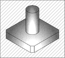
- the inspection apparatus 1 is an apparatus that inspects the appearance of a three-dimensional object 9 having a glossy surface.
- the object 9 is, for example, a metal part formed by forging or casting, and the surface thereof has a matte shape with minute irregularities.
- the object 9 is, for example, various parts (cylindrical hub shaft, outer ring, yoke, etc.) used for universal joints.
- the inspection apparatus 1 includes a main body 11 and a computer 12.
- the main body 11 includes a stage 2, a stage rotating unit 21, an imaging unit 3, and a light source unit 4.
- the object 9 is placed on the stage 2.
- the stage rotation unit 21 rotates the object 9 together with the stage 2 by a predetermined angle about the central axis J1 that faces in the up-down direction.
- the central axis J1 passes through the center of the stage 2.
- the main body 11 is provided with a light shielding cover (not shown) that prevents external light from reaching the stage 2, and the stage 2, the imaging unit 3, and the light source unit 4 are provided within the light shielding cover.
- the imaging unit 3 includes one upper imaging unit 31, four oblique imaging units 32, and four side imaging units 33.
- the upper imaging unit 31 is not shown (the same applies to the upper light source unit 41 described later).
- the upper imaging unit 31 is disposed on the central axis J1 above the stage 2. An image obtained by imaging the object 9 on the stage 2 from directly above can be acquired by the upper imaging unit 31.
- the four oblique imaging units 32 are arranged around the stage 2. .
- the four oblique imaging units 32 are arranged at an angular interval (pitch) of 90 ° in the circumferential direction around the central axis J1.
- an angle ⁇ 2 formed by the imaging optical axis K2 and the central axis J1 is approximately 45 °.
- Each oblique imaging unit 32 can acquire an image obtained by imaging the object 9 on the stage 2 from above.
- the four side imaging units 33 are also arranged around the stage 2 in the same manner as the four oblique imaging units 32.
- the four side imaging units 33 are arranged at an angular interval of 90 ° in the circumferential direction.
- the angle ⁇ 3 formed by the imaging optical axis K3 and the central axis J1 is approximately 90 °.
- the upper imaging unit 31, the oblique imaging unit 32, and the side imaging unit 33 have, for example, a CCD (Charge (CoupledupDevice), a CMOS (Complementary Metal-Oxide Semiconductor), and the like, and acquire multi-gradation images.
- the upper imaging unit 31, the oblique imaging unit 32, and the side imaging unit 33 are supported by a support unit (not shown).
- the light source unit 4 includes one upper light source unit 41, eight oblique light source units 42, and eight side light source units 43.
- the upper light source unit 41 is a light source unit in which a plurality of LEDs (light emitting diodes) are arranged in a ring shape centered on the central axis J1.
- the ring-shaped upper light source unit 41 is fixed to the upper imaging unit 31 so as to surround the upper imaging unit 31.
- the upper light source unit 41 can irradiate the object 9 on the stage 2 from directly above along a direction parallel to the central axis J1.
- each oblique light source unit 42 is a light source unit in which a plurality of LEDs are arranged in a bar shape extending in the tangential direction of the circumference around the central axis J1.
- an “illumination axis” a line connecting the center of the emission surface of each oblique light source section 42 and the object 9 (the center thereof) is called an “illumination axis”
- the plane including the illumination axis and the central axis J1 of the oblique light source section 42 is.
- Each oblique light source unit 42 can irradiate the object 9 on the stage 2 along the illumination axis from obliquely above.
- four of the eight oblique light source units 42 are fixed to the four oblique imaging units 32, and the remaining four oblique light source units 42 are illustrated. It is supported by the omitted support part.
- each side light source unit 43 is a light source unit in which a plurality of LEDs are arranged in a bar shape extending in the tangential direction of the circumference around the central axis J1.
- an illumination axis when a line connecting the center of the emission surface of each side light source unit 43 and the object 9 is referred to as an “illumination axis”, the illumination axis and the central axis J 1 of the side light source unit 43.
- Each side light source unit 43 can irradiate the object 9 on the stage 2 from the side along the illumination axis.
- four of the eight side light source units 43 are fixed to the four side imaging units 33, and the remaining four side light source units 43 are illustrated. It is supported by the omitted support part.
- the distance between the upper imaging unit 31 and the upper light source unit 41 and the object 9 is about 55 cm (centimeter).
- the distance between the oblique imaging unit 32 and the oblique light source unit 42 and the object 9 is about 50 cm, and the distance between the side imaging unit 33 and the side light source unit 43 and the object 9 is about 40 cm.
- a light source of a type other than an LED may be used.
- FIG. 3 is a block diagram showing a functional configuration realized by the computer 12.
- the computer 12 includes a control unit 60 and a defect detection unit 61.
- the control unit 60 is responsible for overall control of the inspection apparatus 1.
- the defect detection unit 61 includes a defect candidate detection unit 62 and a defect identification unit 63.
- the defect candidate detection unit 62 detects a defect candidate area based on the captured image acquired by the imaging unit 3.
- the defect specifying unit 63 specifies a defect area indicating a true defect from the defect candidate areas. Details of the defect candidate detection unit 62 and the defect identification unit 63 will be described later.
- FIG. 4 is a diagram showing a flow of processing for inspecting the object 9 by the inspection apparatus 1.
- the object 9 to be inspected is placed on the stage 2 (step S11).
- a plurality of pins for alignment are provided, and an object is placed at a predetermined position on the stage 2 by bringing a predetermined portion of the object 9 into contact with the plurality of pins. 9 are arranged in a predetermined direction.
- imaging setting information for the object 9 on the stage 2 is acquired based on an input by the operator or the like (step S12).
- the imaging setting information includes an imaging unit used in the imaging unit 3 (hereinafter referred to as a “selected imaging unit”), a light source unit that is turned on in the light source unit 4 when the selected imaging unit acquires a captured image, and Indicates.
- selected imaging unit an imaging unit used in the imaging unit 3
- light source unit that is turned on in the light source unit 4 when the selected imaging unit acquires a captured image
- the imaging setting information in this processing example indicates that the four oblique imaging units 32 in the imaging unit 3 are used as the selective imaging units.
- the imaging setting information is obtained with respect to each of the oblique imaging units 32 that are the selected imaging units, and to the oblique light source unit 42 at the same position as the oblique imaging unit 32 and clockwise with respect to the oblique light source unit 42.
- the two oblique light source units 42 adjacent to each other and the two oblique light source units 42 adjacent to each other in the counterclockwise direction hereinafter, these oblique light source units 42 are referred to as “specific light source unit group”). Acquisition of an image to turn on and acquisition of an image to light all of the specific light source group.
- the illumination axes of the five oblique light source units 42 included in the specific light source unit group for each oblique imaging unit 32 are the imaging light of the oblique imaging unit 32. Inclined by ⁇ 90 °, ⁇ 45 °, 0 °, + 45 °, and + 90 °, respectively, with respect to the axis K2. That is, the five oblique light source units 42 are ⁇ 90 °, ⁇ 45 °, 0 °, + 45 °, and + 90 °, respectively, with respect to the oblique imaging unit 32 in the circumferential direction around the central axis J1. Located at an angular position.
- one oblique imaging unit 32 among the plurality of oblique imaging units 32, each of which is a selected imaging unit, is designated as an attention imaging unit (step S13).
- a captured image is acquired by the focused imaging unit 32 while only one oblique light source unit 42 of the specific light source unit group for the focused imaging unit 32 is turned on.
- a region approximately facing the imaging unit 32 of interest on the surface of the object 9 is defined as a “target region”, and light is irradiated along the illumination axis from the oblique light source unit 42 to the target region.
- the target imaging unit 32 images the target region while irradiating light from only one direction by the one oblique light source unit 42 included in the specific light source unit group.
- a captured image acquired by the target imaging unit by irradiation of light from only one light source unit is referred to as a “first captured image”, and light is applied to the target region when acquiring the first captured image.
- the light source part to irradiate is called a “first illumination part”.
- a shadow due to minute unevenness in the target region is likely to occur.
- a plurality of first captured images are obtained by the attention imaging unit 32 by sequentially using each of the plurality of oblique light source units 42 included in the specific light source unit group as the first illumination unit under the control of the control unit 60. Is acquired (step S14).
- the specific light source unit group includes the oblique light source unit 42 at angular positions of ⁇ 90 °, ⁇ 45 °, 0 °, + 45 °, and + 90 ° with respect to the imaging unit 32 of interest.
- first captured image by N ° illumination When the first captured image obtained using the light source unit at the N ° angular position with respect to the target imaging unit as the first illumination unit is referred to as “first captured image by N ° illumination”, in step S14, ⁇ 90 First captured image with illumination of °, first captured image with illumination of -45 °, first captured image with illumination of 0 °, first captured image with illumination of + 45 °, and first imaging with illumination of + 90 ° An image is acquired.
- the plurality of oblique light source units 42 included in the specific light source unit group can be regarded as a plurality of first illumination units used for acquiring a plurality of first captured images. Note that each oblique light source unit 42 included in the specific light source unit group does not necessarily irradiate the entire target region.
- the oblique light source unit 42 at an angular position of ⁇ 90 ° is approximately equal to the target region. Irradiate half of the light.
- the light source unit used as the first illuminating unit may irradiate light from only one direction with respect to each position of the region where light irradiation is possible in the target region.
- a captured image is acquired by the focused imaging unit 32 while all the oblique light source units 42 included in the specific light source unit group for the focused imaging unit 32 are turned on (step S15).
- light from a plurality of oblique light source units 42 at angular positions of ⁇ 90 °, ⁇ 45 °, 0 °, + 45 °, and + 90 ° with respect to the target imaging unit 32 is applied to the target region along the illumination axis. Is irradiated.
- the target imaging unit 32 images the target region while irradiating the target region with light from a plurality of different directions by the plurality of oblique light source units 42.
- the captured image acquired by the target imaging unit by irradiating light from all the light source units included in the specific light source unit group is referred to as a “second captured image”, and the second captured image is acquired.
- a set of all light source units that irradiate the object 9 with light is referred to as a “second illumination unit”.
- each oblique light source unit 42 included in the specific light source unit group does not necessarily irradiate the entire target region with light, but at least 2 in each position of the target region by the second illumination unit.
- Light is emitted from the oblique light source units 42, that is, from at least two directions.
- each position of the target region is irradiated with light from at least three oblique light source units.
- the intensity of light emitted from the plurality of oblique light source units 42 included in the specific light source unit group is substantially the same.
- the intensity of light from each oblique light source unit 42 at the time of acquiring the second captured image is smaller than the intensity of light from the oblique light source unit 42 at the time of acquiring the first captured image.
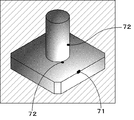
- FIG. 5 to 7 are diagrams showing an example of the first captured image.
- FIG. 5 shows a first captured image with ⁇ 90 ° illumination
- FIG. 6 shows a first captured image with ⁇ 45 ° illumination
- FIG. 7 shows a first captured image with 0 ° illumination.
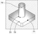
- FIG. 8 is a diagram illustrating an example of the second captured image.
- the second captured image is acquired by light irradiation from the second illumination unit, that is, all illumination of ⁇ 90 °, ⁇ 45 °, 0 °, + 45 °, and + 90 °. 5 to 8, the region indicating the background of the object 9 is indicated by parallel diagonal lines.
- a defect area that shows a concave or convex defect in the target area is usually irradiated from a certain direction.
- the difference in brightness with respect to the surrounding area increases due to the light that is emitted.
- the difference in brightness of the defect area with respect to the surrounding area becomes slight with light irradiated from other directions.
- the defect area has brightness that can be distinguished from the surrounding area by illumination at ⁇ 45 °, and the defect area is difficult to distinguish by illumination in other directions.
- the first captured image of FIG. 6 with ⁇ 45 ° illumination and the second captured image of FIG. 8 with all ⁇ 90 °, ⁇ 45 °, 0 °, + 45 °, and + 90 ° illumination is a brightness that can be distinguished from surrounding areas.
- a false defect area there is a region where the brightness is different from the surrounding region, that is, a false defect region, due to the matte surface of the target region.
- the position where the false defect area is generated is different from that of the first captured image.
- the true defect area 71 and the false defect area 72 are blacked out. Actually, it is impossible to distinguish between the true defect area and the false defect area at the present stage. Of course, the false defect area 72 may also occur in other first captured images.
- a plurality of first captured images by illumination of each oblique light source unit 42 included in the specific light source unit group, and second captured images by illumination of all the oblique light source units 42 included in the specific light source unit group are detected as defects. It is input to the defect candidate detection unit 62 of the unit 61.
- FIG. 9 is a diagram illustrating a configuration of the defect candidate detection unit 62.
- the defect candidate detection unit 62 a first reference image corresponding to each first captured image and a second reference image corresponding to the second captured image are stored in advance.
- the first reference image corresponding to each first captured image is an image that is acquired under the same conditions as the first captured image and indicates a target region that does not include a defect.
- the first reference image is acquired, for example, by performing the same process as in step S14 on an object that does not include a defect, and is stored in the defect candidate detection unit 62.
- a first reference image corresponding to the first captured image may be generated by performing predetermined processing on each first captured image. The same applies to the second reference image corresponding to the second captured image.
- each of the plurality of first captured images and second captured images is simply “imaging”.
- the first or second reference image corresponding to the captured image is simply referred to as a “reference image”.
- filter processing for removing noise such as a median filter and a Gaussian filter is performed on the captured image and the reference image, respectively, and the filtered captured image and reference image are sent to the pre-alignment unit 622. Entered.
- the pre-alignment unit 622 the amount of positional deviation and angle shift relative to the reference image of the (filtered) captured image is specified by pattern matching using a predetermined pattern. Then, the position and angle of the captured image are adjusted to the reference image by translating and rotating the captured image with respect to the reference image by an amount of position and angle deviation between the two images (that is, pre-alignment is performed). .
- the sway comparator 623 evaluates the difference between the moved captured image and the reference image when the captured image is moved from the pre-aligned position with respect to the reference image to each of a plurality of two-dimensionally arranged positions.
- a value for example, a sum of pixel value differences (absolute values) in a region where both images overlap
- an image indicating a difference (absolute value) between pixel values of both images at a position where the evaluation value is minimum is binarized with a predetermined threshold value, and a binary defect candidate image is output.
- the defect candidate detection unit 62 compares each captured image with the reference image corresponding to the captured image, thereby determining a defect candidate region in the target region (hereinafter referred to as “defect candidate region”).
- the defect candidate image shown is generated. In other words, a defect candidate area in the target area is detected based on the captured image.
- the defect candidate detection unit 62 compares each first captured image with the first reference image corresponding to the first captured image, so that the first defect candidate image indicating the first defect candidate region is obtained.
- the first defect candidate region is generated and detected (step S16).
- a second defect candidate image indicating the second defect candidate region is generated, and the second defect candidate region is detected.
- the first defect candidate image acquired from the first captured image with N ° illumination is referred to as “first defect candidate image with N ° illumination”
- the first defect with ⁇ 90 ° illumination is obtained.
- FIG. 10 is a diagram showing a first defect candidate image derived from ⁇ 45 ° illumination derived from the first captured image of FIG. 6, and FIG. 11 is ⁇ 90 °, ⁇ derived from the second captured image of FIG. 8. It is a figure which shows the 2nd defect candidate image by all the illumination of 45 degrees, 0 degrees, +45 degrees, and +90 degrees.
- the first defect candidate image in FIG. 10 is a binary image showing the true defect area 71 and the false defect area 72 in FIG. 6 as the first defect candidate area 73.
- the second defect candidate image in FIG. 11 is a binary image showing the true defect area 71 and the false defect area 72 in FIG. 8 as the second defect candidate area 74.
- the plurality of first defect candidate images and second defect candidate images are output to the defect specifying unit 63.
- FIG. 12 is a diagram showing the configuration of the defect identification unit 63.
- Pixel values of a plurality of first defect candidate images with illumination of ⁇ 90 °, ⁇ 45 °, 0 °, + 45 °, and + 90 ° are sequentially input to the plurality of AND operation units 631, respectively.
- pixel values of the second defect candidate image are also sequentially input to the plurality of AND operation units 631.
- each logical product operation unit 631 obtains a logical product of the value of each pixel of the second defect candidate image and the value of the corresponding pixel of the first defect candidate image, and outputs the logical product to the logical sum operation unit 632.
- each AND operation unit 631 when the second defect candidate image and the first defect candidate image are accurately overlapped, the pixel of the region where the second defect candidate region 74 and the first defect candidate region 73 overlap is used. On the other hand, a value indicating a defective area is output. In addition, a value indicating a non-defective region is output for a pixel in a region where the second defect candidate region 74 and the first defect candidate region 73 do not overlap. In this manner, the overlapping area in the second defect candidate area 74 and the first defect candidate area 73 is substantially specified as the defect area in the target area.
- the logical sum operation unit 632 obtains the logical sum of the values input from the plurality of logical product operation units 631 for each pixel of the second defect candidate image and outputs it to the area filter unit 633. That is, for each pixel of the second defect candidate image, when a value indicating a defective area is input from any of the AND operation units 631, a value indicating the defective area is output to the area filter unit 633, When a value indicating a non-defective region is input from the AND operation unit 631, a value indicating a non-defective region is output to the area filter unit 633.
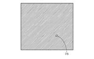
- an image is generated in which the value input from the OR operation unit 632 for each pixel of the second defect candidate image is used as the position value of the pixel.
- a set of pixels that have a value indicating the defect area and are continuous with each other is specified as the defect area, and is included in the defect area when the area of the defect area is less than a predetermined area threshold value.
- the value of the pixel is changed to a value indicating a non-defective area.
- the value of the pixel in the defect region having an area equal to or larger than the area threshold value remains unchanged.
- the control unit 60 it is confirmed whether or not all the selected imaging units are designated as the target imaging unit.
- the other oblique imaging unit 32 is specified as the target imaging unit (step S13).
- the four oblique imaging units 32 are arranged at an angular interval of 90 ° in the circumferential direction.
- the area of the target 9 for which no area image has been acquired is the target area for the target imaging unit 32.
- Step S14 When the target imaging unit 32 is specified, five first captured images obtained by illumination at ⁇ 90 °, ⁇ 45 °, 0 °, + 45 °, and + 90 ° with respect to the target region are acquired in the same manner as described above.
- Step S14 second captured images obtained by all illumination of ⁇ 90 °, ⁇ 45 °, 0 °, + 45 °, and + 90 ° are acquired (step S15).
- a first defect candidate image is generated by comparing each first captured image with a first reference image corresponding to the first captured image (step S16), and corresponds to the second captured image and the second captured image.
- a second defect candidate image is generated by comparing with the second reference image (step S17).
- a defect area image for the target area is acquired from each first defect candidate image and second defect candidate image (step S18).
- the processing related to the acquisition of the defective area image is performed using all the selected imaging units as the target imaging unit (step S19). Thereby, a defect area image is acquired for each of the four target areas arranged at an angular interval of 90 ° in the circumferential direction in the target object 9.
- the control unit 60 confirms whether or not the stage 2 has been rotated a predetermined number of times.
- the stage rotating unit 21 rotates the stage 2 by 45 ° about the central axis J1 (step S21).
- steps S13 to S18 are repeated (step S19).
- a defect region image is acquired for each of the eight target regions arranged in the target object 9 at an angular interval of 45 ° in the circumferential direction.
- the eight target regions are continuous over the entire circumference in the circumferential direction, defects in the object 9 are detected over the entire circumference in the circumferential direction.
- the eight target regions may partially overlap each other.
- the control unit 60 confirms that the stage 2 has been rotated a predetermined number of times, and the inspection of the object 9 is completed (step S20).
- four oblique imaging units 32 are designated as selective imaging units, and ⁇ 90 °, ⁇ 45 °, 0 °, + 45 °, +90 with respect to each oblique imaging unit 32 that is the selective imaging unit.
- the selected imaging unit and the specific light source unit group may be other combinations.
- four side imaging units 33 are designated as selective imaging units, and angles of ⁇ 90 °, ⁇ 45 °, 0 °, + 45 °, and + 90 ° with respect to each side imaging unit 33 that is the selective imaging unit.
- a plurality of side light source units 43 may be used as the specific light source unit group for the oblique imaging unit 32 that is the selective imaging unit, and a plurality of oblique sources are used for the side imaging unit 33 that is the selective imaging unit.
- the light source unit 42 may be used as a specific light source unit group.
- the upper imaging unit 31 may be designated as the selected imaging unit, and the upper light source unit 41 may be used as one of the specific light source unit groups.
- the specific light source unit group may include an upper light source unit 41, an oblique light source unit 42, and a side light source unit 43.
- the number of light source units used as the specific light source unit group for each selected imaging unit is preferably 3 or more (for example, 5 or less).
- various image pickup units are designated as selected image pickup units, and various plural light source units are used as specific light source unit groups for each selected image pickup unit, thereby enabling highly accurate defect detection. .
- a plurality of light source units that respectively irradiate light from a plurality of directions to a target region that faces the imaging unit are provided, and one light source unit among the plurality of light source units is provided.
- the first captured image is acquired by the imaging unit by irradiation of light from the second imaging unit
- the second captured image is acquired by the imaging unit by irradiation of light from the plurality of light source units.
- the first defect candidate region is detected by comparing the first captured image with the first reference image corresponding to the first captured image, and the second reference corresponding to the second captured image and the second captured image is detected.
- the second defect candidate area is detected by comparing the image.
- an overlapping area in the first defect candidate area and the second defect candidate area is specified as a defect area in the target area.
- a plurality of first captured images are acquired by the imaging unit. Further, by comparing the plurality of first captured images and the plurality of first reference images corresponding to the plurality of first captured images, respectively, a plurality of first defect candidates each indicating a first defect candidate region. An image is generated. And the 1st defect candidate area
- a plurality of first captured images are acquired using a plurality of light source units for one target region (imaging position of one imaging unit), and the target region is based on the plurality of first captured images.
- the defect on the surface of the object 9 can be detected more stably (more reliably).
- the inspection apparatus 1 by providing the upper imaging unit 31, the plurality of oblique imaging units 32, and the plurality of side imaging units 33, the blind spot in the object 9 can be reduced, and the inspection of the object 9 is performed. Reliability can be improved.
- the inspection apparatus 1 can be variously modified.
- the inspection apparatus 1 eight oblique imaging units 32 are provided at the same position as the eight oblique light source units 42, and eight side imaging units 33 are disposed at the same position as the eight side light source units 43. It may be provided. In this case, the defect of the object 9 can be detected in a short time over the entire circumference in the circumferential direction while omitting the rotation of the stage 2 in step S21 of FIG. Further, in order to reduce the manufacturing cost of the inspection apparatus 1, the two oblique imaging units 32 and the two side imaging units 33 are omitted in FIG.
- the remaining two oblique imaging units 32 are provided at an angular interval of 180 ° in the circumferential direction, and the remaining two side imaging units 33 are provided at an angular interval of 180 ° in the circumferential direction.
- the number of rotations of the stage 2 in step S20 is set to 3 times.
- only one upper imaging unit 31, one oblique imaging unit 32, and one side imaging unit 33 are provided in the imaging unit 3, and the light source unit 4, only one upper light source unit 41, five oblique light source units 42 and five side light source units 43 may be provided.
- the five oblique light source units 42 are arranged at angular positions of ⁇ 90 °, ⁇ 45 °, 0 °, + 45 °, and + 90 ° with respect to the oblique imaging unit 32, and the five lateral light source units 43 are These are arranged at angular positions of ⁇ 90 °, ⁇ 45 °, 0 °, + 45 °, and + 90 ° with respect to the side imaging unit 33.
- the number of rotations of the stage 2 in step S20 is set to 7 times.
- the stage 2 may be fixed, and the imaging unit 3 and the light source unit 4 may rotate about the central axis J1.
- a central axis J1 that faces in a direction other than the vertical direction (the direction of gravity) may be set.
- only one of the first defect candidate image and the second defect candidate image is generated for one selected imaging unit, and the defect candidate area indicated by the defect candidate image is treated as a defect area. Also good.
- a plurality of light source units that irradiate the target region with light from a plurality of directions are provided as the second illumination unit, and one of the plurality of light source units is the first illumination unit.
- the 1st illumination part 51 and the 2nd illumination part 52 may be provided separately.
- the first illumination unit 51 can irradiate light from only one direction on the target region on the surface of the object 9, and the second illumination unit 52 can irradiate light from a plurality of directions on the target region. It is.
- the first illumination unit 51 is fixed to the upper surface of the imaging unit 30, and the second illumination unit 52 is fixed to the lower surface of the imaging unit 30.
- the 2nd illumination part 52 several LED is arranged in the circular arc shape along the circumferential direction.
- a plurality of first illumination units 51 that irradiate light from a plurality of different directions to the target region are provided, It is preferable that a plurality of first captured images indicating the target region are acquired using the plurality of first illumination units 51.
- the 1st illumination part 51 is abbreviate
- the first illumination unit emits light from substantially only one direction with respect to the target region, for example, the first illumination unit irradiates the target region with a plurality of light sources slightly separated (separated). It may be a thing. From the viewpoint of different imaging conditions (positions where false defect regions are generated) between the second captured image acquired using the second illumination unit and the first captured image acquired using the first illumination unit, It is preferable that the illumination direction of the light with respect to each position of the object area
- the generation of the candidate image and the generation of the second defect candidate image from the second captured image have been described as being sequentially performed. For example, after the acquisition of the first captured image, the acquisition of the second captured image, and the first The generation of defect candidate images may be performed in parallel. Further, the first captured images of the plurality of target areas may be sequentially acquired by the plurality of selected imaging units, and then the second captured images of the plurality of target areas may be sequentially acquired. In this way, the processing flow of FIG. 4 can be changed as appropriate.
- a plate-like or film-like object having a satin-like region on the surface may be inspected.
- the inspection apparatus 1 is particularly suitable for inspecting an object having a satin-like region on the surface, which is a metal surface, but the appearance of an object having a satin-like region on the surface, which is the surface of a material other than metal, is on the surface.
- the inspection apparatus 1 may inspect.
Landscapes
- General Physics & Mathematics (AREA)
- Physics & Mathematics (AREA)
- Immunology (AREA)
- Pathology (AREA)
- Analytical Chemistry (AREA)
- Biochemistry (AREA)
- General Health & Medical Sciences (AREA)
- Life Sciences & Earth Sciences (AREA)
- Health & Medical Sciences (AREA)
- Chemical & Material Sciences (AREA)
- Engineering & Computer Science (AREA)
- Computer Vision & Pattern Recognition (AREA)
- Signal Processing (AREA)
- Quality & Reliability (AREA)
- Theoretical Computer Science (AREA)
- Investigating Materials By The Use Of Optical Means Adapted For Particular Applications (AREA)
- Image Processing (AREA)
Abstract
Description
9 対象物
30~33 撮像部
41~43 光源部
51 第1照明部
52 第2照明部
60 制御部
62 欠陥候補検出部
63 欠陥特定部
73 第1欠陥候補領域
74 第2欠陥候補領域
75 欠陥領域
S11~S21 ステップ
Claims (8)
- 表面に梨地状の領域を有する対象物の外観を検査する検査装置であって、
対象物の表面における所定の対象領域に対して一の方向のみから光を照射する第1照明部と、
前記対象領域に対して複数の方向から光を照射する第2照明部と、
前記対象領域を撮像する撮像部と、
前記第1照明部からの光の照射により前記撮像部にて取得される第1撮像画像と前記第1撮像画像に対応する第1参照画像とを比較することにより、前記対象領域における欠陥候補の領域を第1欠陥候補領域として検出し、前記第2照明部からの光の照射により前記撮像部にて取得される第2撮像画像と前記第2撮像画像に対応する第2参照画像とを比較することにより、前記対象領域における欠陥候補の領域を第2欠陥候補領域として検出する欠陥候補検出部と、
前記第1欠陥候補領域および前記第2欠陥候補領域において重複する領域を、前記対象領域における欠陥領域として特定する欠陥特定部と、
を備える。 - 請求項1に記載の検査装置であって、
前記第2照明部が、前記対象領域に対して複数の方向からそれぞれ光を照射する複数の光源部を有し、
前記複数の光源部のうちの一の光源部が、前記第1照明部である。 - 請求項2に記載の検査装置であって、
前記複数の光源部のそれぞれを前記第1照明部として順次用いることにより、前記撮像部に複数の第1撮像画像を取得させる制御部をさらに備え、
前記欠陥候補検出部が、前記複数の第1撮像画像と、前記複数の第1撮像画像に対応する複数の第1参照画像とをそれぞれ比較することにより、それぞれが第1欠陥候補領域を示す複数の第1欠陥候補画像を生成し、
前記欠陥特定部が、各第1欠陥候補画像が示す前記第1欠陥候補領域、および、前記第2欠陥候補領域において重複する領域を、前記対象領域における欠陥領域として特定する。 - 請求項2または3に記載の検査装置であって、
前記複数の光源部の個数が3以上である。 - 表面に梨地状の領域を有する対象物の外観を検査する検査方法であって、
a)対象物の表面における所定の対象領域に対して、第1照明部により一の方向のみから光を照射しつつ、前記対象領域を撮像する撮像部にて第1撮像画像を取得する工程と、
b)前記対象領域に対して第2照明部により複数の方向から光を照射しつつ、前記撮像部にて第2撮像画像を取得する工程と、
c)前記第1撮像画像と前記第1撮像画像に対応する第1参照画像とを比較することにより、前記対象領域における欠陥候補の領域を第1欠陥候補領域として検出する工程と、
d)前記第2撮像画像と前記第2撮像画像に対応する第2参照画像とを比較することにより、前記対象領域における欠陥候補の領域を第2欠陥候補領域として検出する工程と、
e)前記第1欠陥候補領域および前記第2欠陥候補領域において重複する領域を、前記対象領域における欠陥領域として特定する工程と、
を備える。 - 請求項5に記載の検査方法であって、
前記第2照明部が、前記対象領域に対して複数の方向からそれぞれ光を照射する複数の光源部を有し、
前記複数の光源部のうちの一の光源部が、前記第1照明部である。 - 請求項6に記載の検査方法であって、
前記a)工程において、前記複数の光源部のそれぞれを前記第1照明部として順次用いることにより、前記撮像部にて複数の第1撮像画像が取得され、
前記c)工程において、前記複数の第1撮像画像と、前記複数の第1撮像画像に対応する複数の第1参照画像とをそれぞれ比較することにより、それぞれが第1欠陥候補領域を示す複数の第1欠陥候補画像が生成され、
前記e)工程において、各第1欠陥候補画像が示す前記第1欠陥候補領域、および、前記第2欠陥候補領域において重複する領域が、前記対象領域における欠陥領域として特定される。 - 請求項6または7に記載の検査方法であって、
前記複数の光源部の個数が3以上である。
Priority Applications (4)
| Application Number | Priority Date | Filing Date | Title |
|---|---|---|---|
| KR1020177006857A KR101931456B1 (ko) | 2014-09-05 | 2015-04-28 | 검사 장치 및 검사 방법 |
| US15/507,950 US10705029B2 (en) | 2014-09-05 | 2015-04-28 | Inspection apparatus and inspection method |
| CN201580047339.XA CN106796179B (zh) | 2014-09-05 | 2015-04-28 | 检查装置以及检查方法 |
| EP15838785.2A EP3190401B1 (en) | 2014-09-05 | 2015-04-28 | Inspection device and inspection method |
Applications Claiming Priority (2)
| Application Number | Priority Date | Filing Date | Title |
|---|---|---|---|
| JP2014181054A JP6370177B2 (ja) | 2014-09-05 | 2014-09-05 | 検査装置および検査方法 |
| JP2014-181054 | 2014-09-05 |
Publications (1)
| Publication Number | Publication Date |
|---|---|
| WO2016035381A1 true WO2016035381A1 (ja) | 2016-03-10 |
Family
ID=55439455
Family Applications (1)
| Application Number | Title | Priority Date | Filing Date |
|---|---|---|---|
| PCT/JP2015/062872 WO2016035381A1 (ja) | 2014-09-05 | 2015-04-28 | 検査装置および検査方法 |
Country Status (7)
| Country | Link |
|---|---|
| US (1) | US10705029B2 (ja) |
| EP (1) | EP3190401B1 (ja) |
| JP (1) | JP6370177B2 (ja) |
| KR (1) | KR101931456B1 (ja) |
| CN (1) | CN106796179B (ja) |
| TW (1) | TWI580951B (ja) |
| WO (1) | WO2016035381A1 (ja) |
Cited By (4)
| Publication number | Priority date | Publication date | Assignee | Title |
|---|---|---|---|---|
| CN109564167A (zh) * | 2016-08-18 | 2019-04-02 | 株式会社斯库林集团 | 检查装置及检查方法 |
| CN110234984A (zh) * | 2017-03-23 | 2019-09-13 | 株式会社斯库林集团 | 照明装置、照明方法以及拍摄装置 |
| EP3546927A4 (en) * | 2017-05-26 | 2020-09-09 | Sintokogio, Ltd. | INSPECTION DEVICE AND CASTING SYSTEM |
| EP3637092A4 (en) * | 2017-06-05 | 2021-03-10 | SCREEN Holdings Co., Ltd. | INSPECTION DEVICE AND INSPECTION PROCEDURE |
Families Citing this family (47)
| Publication number | Priority date | Publication date | Assignee | Title |
|---|---|---|---|---|
| JP6648147B2 (ja) | 2014-10-24 | 2020-02-14 | マジック アイ インコーポレイテッド | 距離センサ |
| US10488192B2 (en) * | 2015-05-10 | 2019-11-26 | Magik Eye Inc. | Distance sensor projecting parallel patterns |
| TW201706563A (zh) | 2015-05-10 | 2017-02-16 | 麥吉克艾公司 | 距離感測器(一) |
| CN107535089B (zh) * | 2015-05-25 | 2019-10-01 | 株式会社富士 | 元件安装机 |
| US10068326B2 (en) * | 2016-03-18 | 2018-09-04 | Siemens Energy, Inc. | System and method for enhancing visual inspection of an object |
| JP6917757B2 (ja) * | 2016-06-15 | 2021-08-11 | 株式会社Screenホールディングス | 外観検査装置、表面処理システム、外観検査方法、プログラム、および投射材交換判断方法 |
| DE102016011497B4 (de) * | 2016-09-21 | 2019-01-24 | Mühlbauer Gmbh & Co. Kg | Optische Untersuchungseinrichtung und optisches Untersuchungsverfahren mit sichtbarem und infrarotem Licht für Halbleiterbauteile |
| JP6499139B2 (ja) * | 2016-10-14 | 2019-04-10 | 矢崎総業株式会社 | 検査装置 |
| JP2020501156A (ja) | 2016-12-07 | 2020-01-16 | マジック アイ インコーポレイテッド | 平行パターンを投射する距離センサ |
| JP7254324B2 (ja) * | 2017-06-05 | 2023-04-10 | 学校法人梅村学園 | 画像検査システムの性能調整のための検査用画像を生成する画像生成装置及び画像生成方法 |
| KR20200054324A (ko) * | 2017-10-08 | 2020-05-19 | 매직 아이 인코포레이티드 | 다중 이동형 센서들을 포함한 센서 시스템의 캘리브레이션 |
| KR20200054326A (ko) | 2017-10-08 | 2020-05-19 | 매직 아이 인코포레이티드 | 경도 그리드 패턴을 사용한 거리 측정 |
| US10679076B2 (en) | 2017-10-22 | 2020-06-09 | Magik Eye Inc. | Adjusting the projection system of a distance sensor to optimize a beam layout |
| CN108132264A (zh) * | 2017-12-19 | 2018-06-08 | 江苏伊莱尔电力科技有限公司 | 一种滤波器成品缺陷检测方法法 |
| CN109961455B (zh) * | 2017-12-22 | 2022-03-04 | 杭州萤石软件有限公司 | 一种目标检测方法及装置 |
| JP7083646B2 (ja) * | 2018-01-15 | 2022-06-13 | 株式会社Screenホールディングス | 錠剤検査方法および錠剤検査装置 |
| CN111602047B (zh) * | 2018-01-15 | 2023-08-18 | 株式会社斯库林集团 | 片剂检查方法以及片剂检查装置 |
| JP7113627B2 (ja) | 2018-02-05 | 2022-08-05 | 株式会社Screenホールディングス | 画像取得装置、画像取得方法および検査装置 |
| JP7170400B2 (ja) * | 2018-02-14 | 2022-11-14 | 株式会社Screenホールディングス | 検査装置、検査方法、錠剤印刷装置および錠剤印刷方法 |
| JP6598898B2 (ja) * | 2018-02-27 | 2019-10-30 | 株式会社Screenホールディングス | 芯ズレ検出装置および芯ズレ検出方法 |
| JP7073785B2 (ja) * | 2018-03-05 | 2022-05-24 | オムロン株式会社 | 画像検査装置、画像検査方法及び画像検査プログラム |
| JP2021518535A (ja) | 2018-03-20 | 2021-08-02 | マジック アイ インコーポレイテッド | 様々な密度の投影パターンを使用する距離測定 |
| US10931883B2 (en) | 2018-03-20 | 2021-02-23 | Magik Eye Inc. | Adjusting camera exposure for three-dimensional depth sensing and two-dimensional imaging |
| JP7076280B2 (ja) * | 2018-04-27 | 2022-05-27 | 日立造船株式会社 | 測定方法および測定装置 |
| JP7292315B2 (ja) | 2018-06-06 | 2023-06-16 | マジック アイ インコーポレイテッド | 高密度投影パターンを使用した距離測定 |
| CN108896566A (zh) * | 2018-07-27 | 2018-11-27 | 佛山市坦斯盯科技有限公司 | 一种aoi相机及光源模组 |
| JP7188930B2 (ja) | 2018-07-27 | 2022-12-13 | 株式会社Screenホールディングス | 刻印検査装置、刻印検査方法および物品検査装置 |
| KR102112053B1 (ko) * | 2018-08-01 | 2020-05-18 | 주식회사 뷰온 | 이미지 센서를 이용한 표면결함 검사장치 및 검사방법 |
| WO2020033169A1 (en) * | 2018-08-07 | 2020-02-13 | Magik Eye Inc. | Baffles for three-dimensional sensors having spherical fields of view |
| EP3853593A4 (en) * | 2018-09-20 | 2021-11-17 | Siemens Healthcare Diagnostics, Inc. | SYSTEMS, METHODS AND TESTING APPARATUS FOR SELF-DIAGNOSIS OF OPTICAL COMPONENTS OF VISION-BASED INSPECTION SYSTEMS |
| CN112889351B (zh) * | 2018-10-25 | 2024-07-26 | 松下知识产权经营株式会社 | 照明控制装置、照明控制系统以及照明控制方法 |
| JP6956063B2 (ja) * | 2018-12-07 | 2021-10-27 | ファナック株式会社 | 加工品の表面損傷検査システム |
| EP3911920B1 (en) | 2019-01-20 | 2024-05-29 | Magik Eye Inc. | Three-dimensional sensor including bandpass filter having multiple passbands |
| WO2020197813A1 (en) | 2019-03-25 | 2020-10-01 | Magik Eye Inc. | Distance measurement using high density projection patterns |
| KR102290802B1 (ko) * | 2019-03-29 | 2021-08-20 | 민팃(주) | 전자 기기 가치 평가 시스템 |
| JP7534330B2 (ja) | 2019-05-12 | 2024-08-14 | マジック アイ インコーポレイテッド | 3次元深度マップデータの2次元画像上へのマッピング |
| JP7444171B2 (ja) * | 2019-09-13 | 2024-03-06 | コニカミノルタ株式会社 | 表面欠陥判別装置、外観検査装置及びプログラム |
| WO2021113135A1 (en) | 2019-12-01 | 2021-06-10 | Magik Eye Inc. | Enhancing triangulation-based three-dimensional distance measurements with time of flight information |
| JP6755603B1 (ja) * | 2019-12-25 | 2020-09-16 | 上野精機株式会社 | 電子部品の処理装置 |
| US11580662B2 (en) | 2019-12-29 | 2023-02-14 | Magik Eye Inc. | Associating three-dimensional coordinates with two-dimensional feature points |
| JP2023510738A (ja) | 2020-01-05 | 2023-03-15 | マジック アイ インコーポレイテッド | 3次元カメラの座標系を2次元カメラの入射位置に移動させる方法 |
| JP7038163B2 (ja) | 2020-05-18 | 2022-03-17 | 本田技研工業株式会社 | 外観検査システム |
| CN111879789A (zh) * | 2020-07-15 | 2020-11-03 | 深圳科瑞技术股份有限公司 | 金属表面缺陷检测方法及系统 |
| CN111812341A (zh) * | 2020-07-22 | 2020-10-23 | 英华达(上海)科技有限公司 | 自动化设备检测系统和检测自动化设备内部运作的方法 |
| DE102020210484A1 (de) * | 2020-08-18 | 2022-02-24 | Magna Steyr Fahrzeugtechnik Ag & Co Kg | Verfahren zum Prüfen einer Konservierungsschicht |
| JP2023043509A (ja) * | 2021-09-16 | 2023-03-29 | アピックヤマダ株式会社 | 外観検査装置及び外観検査方法 |
| CN115356261B (zh) * | 2022-07-29 | 2024-09-20 | 燕山大学 | 一种汽车球笼防尘罩的缺陷检测系统及方法 |
Citations (5)
| Publication number | Priority date | Publication date | Assignee | Title |
|---|---|---|---|---|
| JPH03123808A (ja) * | 1989-10-06 | 1991-05-27 | Sumitomo Electric Ind Ltd | 表面不良検出装置 |
| JPH0678856U (ja) * | 1993-04-09 | 1994-11-04 | 株式会社ロゼフテクノロジー | 照明装置 |
| JP2005214720A (ja) * | 2004-01-28 | 2005-08-11 | Fuji Photo Film Co Ltd | 表面検査装置及び方法 |
| JP2008164628A (ja) * | 2004-07-28 | 2008-07-17 | Byk Gardner Gmbh | 光表面特性の測角検査装置 |
| JP2010139434A (ja) * | 2008-12-12 | 2010-06-24 | Yamatake Corp | 異物とキズ痕との判別検査装置及び検査方法 |
Family Cites Families (20)
| Publication number | Priority date | Publication date | Assignee | Title |
|---|---|---|---|---|
| US5917588A (en) * | 1996-11-04 | 1999-06-29 | Kla-Tencor Corporation | Automated specimen inspection system for and method of distinguishing features or anomalies under either bright field or dark field illumination |
| JPH11108637A (ja) * | 1997-10-03 | 1999-04-23 | Dakku Engineering Kk | 品質検査装置 |
| JP3120767B2 (ja) * | 1998-01-16 | 2000-12-25 | 日本電気株式会社 | 外観検査装置、外観検査方法及び外観検査プログラムを記録した記録媒体 |
| US6198529B1 (en) * | 1999-04-30 | 2001-03-06 | International Business Machines Corporation | Automated inspection system for metallic surfaces |
| US6788404B2 (en) * | 2002-07-17 | 2004-09-07 | Kla-Tencor Technologies Corporation | Inspection system with multiple illumination sources |
| JP2005017234A (ja) | 2003-06-27 | 2005-01-20 | Sony Corp | 外観検査方法、外観検査装置及び電子回路基板の製造装置 |
| JP2007240432A (ja) * | 2006-03-10 | 2007-09-20 | Omron Corp | 欠陥検査装置および欠陥検査方法 |
| US20090116727A1 (en) * | 2006-05-02 | 2009-05-07 | Accretech Usa, Inc. | Apparatus and Method for Wafer Edge Defects Detection |
| KR100755372B1 (ko) | 2006-08-25 | 2007-09-04 | 삼성전자주식회사 | 웨이퍼 검사방법 |
| JP2009162573A (ja) | 2007-12-28 | 2009-07-23 | Ricoh Elemex Corp | 形状認識装置 |
| JP5159373B2 (ja) * | 2008-03-06 | 2013-03-06 | オリンパス株式会社 | 基板検査方法 |
| JP2010151479A (ja) | 2008-12-24 | 2010-07-08 | Ushio Inc | 配線パターン検査装置 |
| SG164292A1 (en) | 2009-01-13 | 2010-09-29 | Semiconductor Technologies & Instruments Pte | System and method for inspecting a wafer |
| SG163442A1 (en) * | 2009-01-13 | 2010-08-30 | Semiconductor Technologies & Instruments | System and method for inspecting a wafer |
| US8532364B2 (en) * | 2009-02-18 | 2013-09-10 | Texas Instruments Deutschland Gmbh | Apparatus and method for detecting defects in wafer manufacturing |
| KR101108672B1 (ko) * | 2009-05-12 | 2012-01-25 | (주)제이티 | 반도체소자 비전검사장치 및 그 방법 |
| CN102822666A (zh) | 2009-11-30 | 2012-12-12 | 株式会社尼康 | 检查装置、三维形状测定装置、构造物的制造方法 |
| KR101324015B1 (ko) * | 2011-08-18 | 2013-10-31 | 바슬러 비전 테크놀로지스 에이지 | 유리기판 표면 불량 검사 장치 및 검사 방법 |
| US9235885B2 (en) * | 2013-01-31 | 2016-01-12 | Applied Materials Israel Ltd | System, a method and a computer program product for patch-based defect detection |
| TWI491871B (zh) | 2013-07-05 | 2015-07-11 | Machvision Inc | 用於光學檢測的照明系統及使用其之檢測系統、檢測方法 |
-
2014
- 2014-09-05 JP JP2014181054A patent/JP6370177B2/ja active Active
-
2015
- 2015-04-28 KR KR1020177006857A patent/KR101931456B1/ko active IP Right Grant
- 2015-04-28 WO PCT/JP2015/062872 patent/WO2016035381A1/ja active Application Filing
- 2015-04-28 US US15/507,950 patent/US10705029B2/en active Active
- 2015-04-28 EP EP15838785.2A patent/EP3190401B1/en active Active
- 2015-04-28 CN CN201580047339.XA patent/CN106796179B/zh active Active
- 2015-06-08 TW TW104118474A patent/TWI580951B/zh not_active IP Right Cessation
Patent Citations (5)
| Publication number | Priority date | Publication date | Assignee | Title |
|---|---|---|---|---|
| JPH03123808A (ja) * | 1989-10-06 | 1991-05-27 | Sumitomo Electric Ind Ltd | 表面不良検出装置 |
| JPH0678856U (ja) * | 1993-04-09 | 1994-11-04 | 株式会社ロゼフテクノロジー | 照明装置 |
| JP2005214720A (ja) * | 2004-01-28 | 2005-08-11 | Fuji Photo Film Co Ltd | 表面検査装置及び方法 |
| JP2008164628A (ja) * | 2004-07-28 | 2008-07-17 | Byk Gardner Gmbh | 光表面特性の測角検査装置 |
| JP2010139434A (ja) * | 2008-12-12 | 2010-06-24 | Yamatake Corp | 異物とキズ痕との判別検査装置及び検査方法 |
Non-Patent Citations (1)
| Title |
|---|
| See also references of EP3190401A4 * |
Cited By (7)
| Publication number | Priority date | Publication date | Assignee | Title |
|---|---|---|---|---|
| CN109564167A (zh) * | 2016-08-18 | 2019-04-02 | 株式会社斯库林集团 | 检查装置及检查方法 |
| US10942131B2 (en) | 2016-08-18 | 2021-03-09 | SCREEN Holdings Co., Ltd. | Inspection apparatus and inspection method |
| CN110234984A (zh) * | 2017-03-23 | 2019-09-13 | 株式会社斯库林集团 | 照明装置、照明方法以及拍摄装置 |
| EP3546927A4 (en) * | 2017-05-26 | 2020-09-09 | Sintokogio, Ltd. | INSPECTION DEVICE AND CASTING SYSTEM |
| US11158041B2 (en) | 2017-05-26 | 2021-10-26 | Sintokogio, Ltd. | Inspection device and casting system |
| EP3637092A4 (en) * | 2017-06-05 | 2021-03-10 | SCREEN Holdings Co., Ltd. | INSPECTION DEVICE AND INSPECTION PROCEDURE |
| US11074684B2 (en) | 2017-06-05 | 2021-07-27 | SCREEN Holdings Co., Ltd. | Inspection apparatus and inspection method |
Also Published As
| Publication number | Publication date |
|---|---|
| EP3190401A1 (en) | 2017-07-12 |
| TWI580951B (zh) | 2017-05-01 |
| JP2016057075A (ja) | 2016-04-21 |
| CN106796179B (zh) | 2020-02-21 |
| EP3190401A4 (en) | 2018-05-09 |
| KR101931456B1 (ko) | 2018-12-20 |
| CN106796179A (zh) | 2017-05-31 |
| EP3190401B1 (en) | 2021-11-24 |
| TW201610421A (zh) | 2016-03-16 |
| US10705029B2 (en) | 2020-07-07 |
| US20170307544A1 (en) | 2017-10-26 |
| JP6370177B2 (ja) | 2018-08-08 |
| KR20170043569A (ko) | 2017-04-21 |
Similar Documents
| Publication | Publication Date | Title |
|---|---|---|
| JP6370177B2 (ja) | 検査装置および検査方法 | |
| JP6486050B2 (ja) | 検査装置および検査方法 | |
| WO2017141611A1 (ja) | 欠陥検出装置、欠陥検出方法およびプログラム | |
| JP5882730B2 (ja) | 外観検査装置及び外観検査方法 | |
| JP4514007B2 (ja) | 被検体の外観形状検査方法及び装置 | |
| WO2017119250A1 (ja) | 欠陥検出装置および欠陥検出方法 | |
| JP6834174B2 (ja) | 外観検査方法および外観検査装置 | |
| JP6812118B2 (ja) | 欠陥検出装置、欠陥検出方法およびプログラム | |
| JP2006138830A (ja) | 表面欠陥検査装置 | |
| WO2018225460A1 (ja) | 検査装置および検査方法 | |
| JP6811540B2 (ja) | 欠陥検出装置、欠陥検出方法およびプログラム | |
| JP5959430B2 (ja) | ボトルキャップの外観検査装置及び外観検査方法 | |
| JP5978002B2 (ja) | 検査方法及び外観検査装置 | |
| JP6688629B2 (ja) | 欠陥検出装置、欠陥検出方法およびプログラム | |
| JP6393663B2 (ja) | 表面検査装置 | |
| WO2024009868A1 (ja) | 外観検査システム、外観検査方法、学習装置および推論装置 | |
| KR20220065545A (ko) | 비정형적 외형을 갖는 제품의 불량을 검사하는 장치 | |
| JP6358884B2 (ja) | 検査装置 |
Legal Events
| Date | Code | Title | Description |
|---|---|---|---|
| 121 | Ep: the epo has been informed by wipo that ep was designated in this application |
Ref document number: 15838785 Country of ref document: EP Kind code of ref document: A1 |
|
| REEP | Request for entry into the european phase |
Ref document number: 2015838785 Country of ref document: EP |
|
| WWE | Wipo information: entry into national phase |
Ref document number: 2015838785 Country of ref document: EP |
|
| WWE | Wipo information: entry into national phase |
Ref document number: 15507950 Country of ref document: US |
|
| NENP | Non-entry into the national phase |
Ref country code: DE |
|
| ENP | Entry into the national phase |
Ref document number: 20177006857 Country of ref document: KR Kind code of ref document: A |