WO2016021400A1 - 放電ランプ点灯装置 - Google Patents
放電ランプ点灯装置 Download PDFInfo
- Publication number
- WO2016021400A1 WO2016021400A1 PCT/JP2015/070683 JP2015070683W WO2016021400A1 WO 2016021400 A1 WO2016021400 A1 WO 2016021400A1 JP 2015070683 W JP2015070683 W JP 2015070683W WO 2016021400 A1 WO2016021400 A1 WO 2016021400A1
- Authority
- WO
- WIPO (PCT)
- Prior art keywords
- switching element
- voltage
- main discharge
- capacitor
- duty ratio
- Prior art date
Links
Images


Classifications
-
- H—ELECTRICITY
- H05—ELECTRIC TECHNIQUES NOT OTHERWISE PROVIDED FOR
- H05B—ELECTRIC HEATING; ELECTRIC LIGHT SOURCES NOT OTHERWISE PROVIDED FOR; CIRCUIT ARRANGEMENTS FOR ELECTRIC LIGHT SOURCES, IN GENERAL
- H05B41/00—Circuit arrangements or apparatus for igniting or operating discharge lamps
- H05B41/14—Circuit arrangements
- H05B41/30—Circuit arrangements in which the lamp is fed by pulses, e.g. flash lamp
- H05B41/34—Circuit arrangements in which the lamp is fed by pulses, e.g. flash lamp to provide a sequence of flashes
Definitions
- the present invention relates to a discharge lamp lighting device, and more particularly to a discharge lamp lighting device that protects a switching element in a discharge lamp lighting device that performs flash lighting repeatedly at high speed.
- Patent Document 1 Japanese Patent Application Laid-Open No. 2001-37095 (Patent Document 1) describes this type of lighting device.
- the lighting device 61 described in Patent Document 1 includes a main discharge capacitor Cm, an output circuit 64, and a control circuit 65 that controls a supply voltage to the main discharge capacitor Cm by pulse width modulation.
- a trigger output circuit 69 The electric charge accumulated in the main discharge capacitor Cm is flash discharged by the flash lamp 62 attached to the trigger socket 63.
- the main discharge capacitor Cm is charged at a predetermined charging speed until the voltage value of the main discharge capacitor Cm reaches a predetermined voltage value, and after reaching the predetermined voltage value, the target voltage value is not reached. Charging is performed at a speed slower than the predetermined charging speed. According to this, it is described that stable charging can be performed even in high-speed repeated light emission.
- Patent Document 2 Japanese Unexamined Patent Application Publication No. 2012-94362 (Patent Document 2) describes a new short arc type flash lamp (not shown).
- This lamp has a pair of main discharge electrodes inside the arc tube, and a rare gas such as xenon is filled in the arc tube at a predetermined pressure to perform flash lighting, for example, with a wavelength of 150 to 200 nm. Vacuum ultraviolet light can also be emitted.
- conventional flash lamps are mainly used for annealing (heat source) and strobe (visible light source), which are premised on instantaneous flash lighting.
- the apparatus is configured using a short arc type flash lamp that emits vacuum ultraviolet light as described in Patent Document 2, the condition of flash lighting and high-speed repeated lighting for a long time is attached to react the chemical substance. It is done.
- Such a lamp has a shorter distance between electrodes than a conventional long arc flash lamp, and a shorter interval for flash discharge. Then, it is necessary to store the electric charge in the capacitor at high speed in preparation for the next flash discharge while flashing at high speed.
- the present invention suppresses a current value at the time of starting to store electric charge in the capacitor, It is an object of the present invention to provide a discharge lamp lighting device that can prevent destruction of the elements and the like.
- the present invention provides a short arc comprising an arc tube and a pair of main discharge electrodes disposed facing each other at a distance of 0.5 to 12.5 mm inside the arc tube.
- a discharge lamp lighting device for lighting a type flash lamp,
- a main discharge capacitor for accumulating electric charge for flash discharge between the main discharge electrodes; and a switching element.
- the main discharge capacitor is configured to boost a voltage of a DC power source by turning on / off the switching element.
- a booster circuit that accumulates charges in A control circuit
- the control circuit when charging the main discharge capacitor, transmits a switch gate active signal that specifies on / off of the switching element to the booster circuit,
- the switch gate active signal has a duty ratio set to a preset initial duty ratio so that a current flowing through the switching element during an ON period of the switching element does not exceed a preset reference overcurrent value.
- the initial duty ratio is 0.1 to 2.0%
- the control circuit is configured such that during the suppression period until the charging voltage of the main discharging capacitor reaches a predetermined reference voltage value that is lower than a target voltage value, the current flowing through the switching element is the reference current value. It is characterized by increasing to a range that does not exceed.
- a trigger electrode is provided inside or outside the arc tube, and the lighting device is a trigger voltage generation circuit for supplying a trigger high voltage to the trigger electrode according to a trigger pulse signal;
- a discharge resistor connected in parallel to the main discharge capacitor, and the control circuit transmits the trigger pulse signal to the trigger voltage generation circuit, and the trigger pulse signal is turned on when the main discharge capacitor is discharged.
- the control circuit stops transmitting the switch gate active signal, or sets the duty ratio of the switch gate active signal to a value smaller than the initial duty ratio, and the current between the main discharge electrodes Is stopped, the supply of electric charge to the main discharge capacitor is resumed by the initial duty ratio. It may be used as the Rukoto.
- the control circuit transmits a switch gate active signal having a fixed period until the trigger pulse signal is turned on after the voltage of the main discharge capacitor reaches the target voltage.
- a discharge lamp lighting device for a short arc type flash lamp when charging and discharging a main discharge capacitor repeatedly at high pressure and at high speed, the current value at the time of starting to store electric charge in the capacitor is suppressed, It is possible to prevent destruction of elements and the like in the circuit.
- FIG. 1 is a view showing a short arc type flash lamp according to the present invention.
- This short arc type flash lamp 1 (hereinafter also referred to as “lamp 1”) includes a cathode 5 and an anode 6 as a pair of main discharge electrodes inside a glass arc tube 2. Sealed at both ends.
- a trigger electrode 7 around which a metal wire or the like is wound is provided outside the arc tube 2.
- the trigger electrode 7 may be provided inside the arc tube 2, and may include auxiliary trigger electrodes 11 and 12 as shown.
- the auxiliary trigger electrodes 11 and 12 are a kind of trigger electrodes. These are preliminary discharge introduction means for generating charged particles in the light emission space before the main discharge.
- a voltage is independently supplied to the trigger electrode 7 and the auxiliary trigger electrodes 11 and 12 from a lighting device 100 described later.
- the inside of the arc tube 2 is filled with a rare gas such as xenon gas at a predetermined pressure.
- a rare gas such as xenon gas
- the static pressure is 0.1 to 1 MPa.
- the separation distance between the tips of the cathode 5 and the anode 6 is 0.5 to 12.5 mm in order to form a short arc.
- the voltage between the main discharge electrodes during flash discharge is 500 V or more. When these conditions are met, vacuum ultraviolet light (VUV light) having a wavelength of 150 to 200 nm is emitted.
- VUV light vacuum ultraviolet light
- FIG. 2 is a block diagram schematically showing a lighting device according to the present invention.
- the lighting device 100 includes a rectifier circuit 120 that rectifies and smoothes the electric power input from the commercial power source 200, and a PFC circuit that is connected to the output side of the rectifier circuit 120 and is a DC power source having a function of improving the power factor. 130, a booster circuit 140 that boosts the output voltage of the PFC circuit 130, a trigger voltage generation circuit 160, a trigger voltage distribution circuit 170, and a control circuit 110 that controls these circuits.
- the voltage necessary for the flash discharge is generated by the booster circuit 140 and charged in the main discharge capacitor Cm.
- the main discharge capacitor Cm is charged by operating a switching element sw1 (see FIG. 3) described later by a switch gate active signal Sc transmitted from the switch gate active signal generating unit 111 of the control circuit 110 to the booster circuit 140.
- the pulse width is modulated and controlled by adjusting the duty ratio.
- the switch gate active signal is a signal that activates the gate of the switching element sw1 in order to turn on the switching element sw1 and charge the main discharge capacitor Cm.
- the duty ratio is a signal that takes either the on or off state.
- the sum of the periods in the on state in the period is the total length of the period. It is a percentage of the total.
- the charging voltage of the main discharging capacitor Cm is, for example, 500 to 2000 V, and the capacitance is 10 to 100 ⁇ F.
- the trigger voltage generation circuit 160 is a circuit for generating a predetermined voltage at the trigger electrode 7.
- the trigger voltage distribution circuit 170 is a circuit for distributing the predetermined voltage generated by the trigger voltage generation circuit 160 to the trigger electrode 7 and the auxiliary trigger electrodes 11 and 12.
- the trigger pulse signal generation unit 112 of the control circuit 110 generates a trigger pulse signal St that triggers flash discharge at a specified fixed frequency, and transmits the trigger pulse signal St to the trigger voltage generation circuit 160. Thereby, flash discharge between the main discharge electrodes can be performed at a constant period.
- the frequency of the trigger pulse signal St is, for example, 5 to 30 Hz.
- Such a control circuit 110 can be realized by a micro control unit, for example.
- the control circuit 110 is instructed through the external interface 300 by a host device such as a light irradiation device using a short arc type flash lamp light source using the discharge lamp lighting device of the present invention.
- the voltage of the main discharge capacitor Cm is detected by the control circuit 110 via the current / voltage measurement unit 150 connected in parallel with the main discharge capacitor Cm.
- the discharge resistor Rd is connected in parallel for safety.
- This resistor also functions as a bleeder resistor for stable operation of the booster circuit 140.
- the resistance of the current / voltage measuring unit 150 can also be configured to serve as the discharge resistance Rd.
- FIG. 3 is a diagram for explaining a booster circuit according to the present invention.
- the booster circuit 140 is preferably of a flyback type using a booster transformer Th, but may be of another type such as a booster chopper that does not use a booster transformer.
- the switching element sw1 using IGBT, FET or the like is provided on the primary side of the booster circuit 140, and the magnetic energy accumulated in the booster transformer Th based on the current flowing during the ON period is converted into the diode D at the time of OFF transition. And is operated to output a boosted voltage.
- the switching element sw1 is charged with the duty ratio being increased in a state where the charge stored in the main discharge capacitor Cm is nearly empty, an overcurrent may flow.
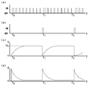
- FIG. 7 is a waveform diagram showing the relationship between a pulse signal and current / voltage created with reference to a charging process in a conventional lighting device.
- This figure is a simulation of a related waveform diagram relating to the lighting device of the present invention shown below.
- (c) the capacitor voltage of the main discharge capacitor Cm, and (d) the switching element current flowing through the switching element sw1 are arranged in a simultaneous series.
- the waveform is a schematic conceptual diagram. In particular, (a) and (b) are intentionally rough drawn so that they are too fine to draw when trying to draw a waveform on the same time scale as the other figures.
- FIG. 4 is a relationship waveform diagram between various signals and current / voltage in the lighting device according to the first embodiment of the present invention.
- This figure shows (a) a switch gate active signal Sc transmitted to the switching element sw1 of the booster circuit, (b) a trigger pulse signal St transmitted to the trigger voltage generation circuit, and (c) a capacitor voltage of the main discharge capacitor Cm. (D) The switching element currents flowing through the switching element sw1 are arranged in a simultaneous series.
- the switch gate active signal Sc is a signal representing a high level / low level corresponding to a period during which the switching element sw1 is turned on / off.
- the switch gate active signal Sc has a preset initial duty ratio so that the current flowing through the switching element during the ON period of the switching element does not exceed a preset reference overcurrent value. Is set. That is, initially, the time for which the switching element sw1 is turned on is set to be short. Specifically, it is turned on only for a time during which the pulse width PW0 is determined by the initial duty ratio.
- the initial duty ratio is preferably 0.1 to 2.0%.
- the pulse frequency is not changed and the pulse width is shortened, but conversely, the pulse width is not changed and the pulse frequency is changed. You may make it low, and you may make it change both pulse frequency and pulse width.
- the duty ratio of the switch gate active signal Sc after the initial duty ratio is adjusted to increase with time.
- the term “enlargement” used herein means that the initial duty ratio has increased until reaching a voltage at which at least an overcurrent does not flow. It may be increased after providing a period for reduction. There is a possibility that an overcurrent flows when charging is started.
- a reference overcurrent value and a reference voltage value lower than the target voltage value of the capacitor are set in advance, and the reference voltage is determined from the voltage at the start of charging.
- a period until the value is reached is defined as a suppression period, and the duty ratio is set so that the switching element current does not exceed the reference overcurrent value during the suppression period.
- the reference overcurrent value and the reference voltage value can be set as appropriate.
- the duty ratio may be adjusted to increase with time until the reference voltage value or the target voltage is reached. This is because, in order to perform flash discharge at a high speed and high pressure such as 10 Hz and 600 V as in the present invention, it is necessary to charge efficiently. That is, initially, the duty ratio is suppressed to prevent overcurrent from flowing through the switching element sw1, and if a certain amount of charge is stored in the main discharge capacitor Cm, the current flowing through the switching element sw1 is Therefore, the speed of charging is increased by increasing the duty ratio in such a way that overcurrent does not flow in the second half.
- the duty ratio is fixed at a substantially constant value. Specifically, the duty ratio is determined according to the difference between the target voltage value and the actually measured capacitor voltage. This is to compensate for a decrease in voltage of the main discharge capacitor Cm due to discharge through the discharge resistor Rd connected in parallel. Since the PWM signal is inserted at a constant period, the capacitor voltage can be kept constant.
- FIG. 4 A second embodiment of the present invention will be described with reference to FIG.
- the capacitor voltage of the capacitor Cm and (d) the switching element current flowing through the switching element sw1 are arranged in a simultaneous series.
- the control circuit 110 stops transmitting the switch gate active signal Sc before the trigger pulse signal St is turned on.
- the duty ratio of the switch gate active signal Sc is set to a value smaller than the initial duty ratio.
- FIG. 5 and FIG. 4 are compared for this effect.
- the trigger pulse signal St is turned on while the duty ratio is substantially fixed.
- the switching element sw1 is turned on with a duty ratio that exceeds the initial duty ratio, so that a slightly higher current flows through the switching element sw1.
- this embodiment shows that the switching element sw1 is turned on while avoiding the period before and after the time when the trigger pulse signal St is turned on. Thereby, the current flowing through the switching element sw1 can be further reduced. That is, priority is given to a decrease in the current value at the expense of the charging operation availability for a moment. Supplementally, even if the timing for turning off the switching element is provided, the discharge resistance Rd is set to a large value of, for example, 10 k ⁇ or more, so that the voltage drop due to the discharge of the main discharge capacitor Cm can be ignored.
- Such control can be realized by the control circuit 110 generating and controlling both the switch gate active signal Sc and the trigger pulse signal St. That is, since the timing at which the trigger pulse signal St is transmitted is determined by the control circuit 110, the switch gate active signal Sc can be set to avoid this.
- the period during which the switching element sw1 is turned off is preferably 0.1 to 2.0 msec before, based on the timing when the trigger pulse signal St is turned on. Yes. This is because, during this period, the influence of a decrease in the charging voltage of the main discharging capacitor Cm is small. Therefore, the trigger pulse signal St is transmitted after 0.1 to 2.0 msec has elapsed since the voltage value of the capacitor reached the target voltage and the switch gate active signal Sc was transmitted last.
- the timing to start charging with the switching element sw1 turned on is after 0.5 to 3.0 msec from the timing when the trigger pulse signal St is turned on, based on research by the inventors. Is known to be preferable. This is because a series of flash discharges in the short arc type flash lamp is completed within this period.
Abstract
本発明は、高圧で高速繰り返し的に主放電用コンデンサの充放電を行う場合に、コンデンサに電荷を蓄え始める際の電流値を抑え、回路中の素子等の破壊を防止することができる放電ランプ点灯装置を提供することを目的とする。 主放電用コンデンサの充電時には、スイッチング素子のオン/オフを規定するスイッチゲートアクティブ信号を昇圧回路へ送信し、主放電用コンデンサの充電電圧が目標電圧値よりも低い所定の基準電圧値に達するまでの抑制期間中は、デューティ比を、スイッチング素子に流れる電流が基準電流値を超えない範囲となるよう増加させる。スイッチゲートアクティブ信号は、スイッチング素子のオン期間中にスイッチング素子に流れる電流が予め設定された基準過電流値を超えないように、デューティ比を0.1~2.0%の大きさの初期デューティ比に設定したものである。
Description
本発明は、放電ランプ点灯装置に関し、特にフラッシュ点灯を高速繰り返し的に行う放電ランプ点灯装置においてスイッチング素子を保護する放電ランプ点灯装置に関するものである。
従来から、高速繰り返し点灯を行うフラッシュランプ用の放電ランプ点灯装置が知られている。
例えば特開2001-37095号公報(特許文献1)には、この種の点灯装置が記載されている。
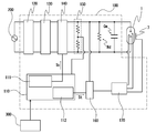
図6に示すように、特許文献1に記載の点灯装置61は、主放電用コンデンサCmと、出力回路64と、パルス幅変調により主放電用コンデンサCmへの供給電圧を制御する制御回路65と、トリガー出力回路69とを備えている。主放電用コンデンサCmに蓄積された電荷は、トリガーソケット63に取り付けられたフラッシュランプ62でフラッシュ放電がされる。
この文献には、主放電用コンデンサCmの電圧値が所定の電圧値になるまでに所定の充電速度で主放電用コンデンサCmを充電し、所定の電圧値に達した後から目標電圧値までは前記所定の充電速度よりも遅い速度で充電する。これによれば、高速繰り返し発光においても安定した充電を行うことができる旨、記載されている。
例えば特開2001-37095号公報(特許文献1)には、この種の点灯装置が記載されている。
図6に示すように、特許文献1に記載の点灯装置61は、主放電用コンデンサCmと、出力回路64と、パルス幅変調により主放電用コンデンサCmへの供給電圧を制御する制御回路65と、トリガー出力回路69とを備えている。主放電用コンデンサCmに蓄積された電荷は、トリガーソケット63に取り付けられたフラッシュランプ62でフラッシュ放電がされる。
この文献には、主放電用コンデンサCmの電圧値が所定の電圧値になるまでに所定の充電速度で主放電用コンデンサCmを充電し、所定の電圧値に達した後から目標電圧値までは前記所定の充電速度よりも遅い速度で充電する。これによれば、高速繰り返し発光においても安定した充電を行うことができる旨、記載されている。
一方、特開2012-94362号公報(特許文献2)には、新型のショートアーク型フラッシュランプが記載されている(不図示)。
このランプは発光管の内部に一対の主放電電極を備えており、発光管の内部に例えばキセノンなどの希ガスを所定の圧力で封入してフラッシュ点灯を行うことにより、例えば波長150~200nmの真空紫外光を放射することもできる。
このランプは発光管の内部に一対の主放電電極を備えており、発光管の内部に例えばキセノンなどの希ガスを所定の圧力で封入してフラッシュ点灯を行うことにより、例えば波長150~200nmの真空紫外光を放射することもできる。
ところで、従来フラッシュランプといえばアニール(熱源)や、ストロボ(可視光源)としての用途が主であり、これらは瞬間的なフラッシュ点灯を前提としたものである。
しかし、特許文献2に記載のような真空紫外光を放射するショートアーク型フラッシュランプを光源として装置を構成する場合は、化学物質を反応させるためにフラッシュ点灯かつ長時間高速繰り返し点灯という条件が付けられる。このようなランプは従来のロングアークフラッシュランプよりも電極間距離が短く、フラッシュ放電する間隔も短い。
すると、高速でフラッシュ点灯しつつ次のフラッシュ放電に備えて高速でコンデンサに電荷を蓄える必要があるが、1度のフラッシュ放電を終えたコンデンサは電荷がほぼ空になっているため、トランスの一次側のL値(インダクタンス)が変化して大きな電流が流れることとなる。この原因は定かではないが、トランスの浮遊容量や配線間の浮遊容量、基板パターン間の浮遊容量などの要因が影響しているものと考えられる。
したがって、従来例の点灯装置を用いるとフラッシュ放電を終えてコンデンサに電荷を蓄え始める際に大きな電流が流れて種々の故障の原因となるおそれがあった。
本発明は、ショートアーク型フラッシュランプ用の放電ランプ点灯装置において、高圧で高速繰り返し的に主放電用コンデンサの充放電を行う場合に、コンデンサに電荷を蓄え始める際の電流値を抑え、回路中の素子等の破壊を防止することができる放電ランプ点灯装置を提供することを目的とする。
上記課題を解決するために、本発明は、発光管と、該発光管内の内部に0.5~12.5mmの距離で離間して対向配置された一対の主放電電極とを備えたショートアーク型フラッシュランプを点灯させる放電ランプ点灯装置であって、
前記主放電電極間のフラッシュ放電のための電荷を蓄積する主放電用コンデンサと、スイッチング素子とを有し、該スイッチング素子のオン/オフにより、DC電源の電圧を昇圧して前記主放電用コンデンサに電荷を蓄積する昇圧回路と、
制御回路とを備え、
該制御回路は、前記主放電用コンデンサの充電時に、前記スイッチング素子のオン/オフを規定するスイッチゲートアクティブ信号を前記昇圧回路へ送信し、
前記スイッチゲートアクティブ信号は、前記スイッチング素子のオン期間中に該スイッチング素子に流れる電流が、予め設定された基準過電流値を超えないように、デューティ比を予め設定された初期デューティ比に設定したものであり、
該初期デューティ比は0.1~2.0%であり、
前記制御回路は、前記主放電用コンデンサの充電電圧が目標電圧値よりも低い所定の基準電圧値に達するまでの抑制期間中は、前記デューティ比を、前記スイッチング素子に流れる電流が前記基準電流値を超えない範囲となるよう増加させるものであることを特徴とする。
また、本発明においては、前記発光管の内部又は外部にはトリガー電極が設けられ、前記点灯装置はトリガーパルス信号に応じて前記トリガー電極にトリガー高電圧を供給するためのトリガー電圧生成回路と、前記主放電用コンデンサに並列接続された放電抵抗とを備え、前記制御回路は、前記トリガーパルス信号を前記トリガー電圧生成回路に送信し、前記主放電用コンデンサの放電時には、前記トリガーパルス信号がオンとなる前に前記制御回路が前記スイッチゲートアクティブ信号を送信することを停止し、若しくは該スイッチゲートアクティブ信号のデューティ比を前記初期デューティ比より小さい値に設定し、前記主放電電極間での電流が停止した後に、前記初期デューティ比により前記主放電用コンデンサへの電荷の供給を再開することとしてもよい。
また、本発明においては、前記制御回路は、前記主放電用コンデンサの電圧が目標電圧に達した後、前記トリガーパルス信号がオンとなるまでは、固定された周期のスイッチゲートアクティブ信号を送信して、前記放電抵抗を介した放電による前記主放電用コンデンサの電圧の低下を補償することとしてもよい。
本発明によれば、ショートアーク型フラッシュランプ用の放電ランプ点灯装置において、高圧で高速繰り返し的に主放電用コンデンサの充放電を行う場合に、コンデンサに電荷を蓄え始める際の電流値を抑え、回路中の素子等の破壊を防止することができる。
図1は本発明に係るショートアーク型フラッシュランプを示す図である。
このショートアーク型フラッシュランプ1(以下、「ランプ1」ともいう。)は、ガラス製の発光管2の内部に一対の主放電電極である陰極5、陽極6を備えていて、発光管2の両端で封止している。発光管2の外部には金属のワイヤーなどを巻き回したトリガー電極7を備えている。
トリガー電極7は発光管2の内部に設けられていてもよく、図示のように補助トリガー電極11、12を備えていても良い。補助トリガー電極11、12はトリガー電極の一種である。これらは主放電の前に発光空間内に荷電粒子を発生させるため予備放電導入手段である。これらのトリガー電極7および補助トリガー電極11、12に対して、後述の点灯装置100より各々独立して電圧が供給される。
発光管2の内部には希ガス、例えばキセノンガスが所定の圧力で封入される。例えば、静圧で0.1~1MPaである。また、陰極5と陽極6の先端の離間距離(主放電電極の電極間距離)は、ショートアークを形成するために0.5~12.5mmである。フラッシュ放電時の主放電電極間での電圧は500V以上となる。このような条件が揃ったときに、波長150~200nmの真空紫外光(VUV光)が放射される。
図2は、本発明に係る点灯装置を模式的に示したブロック図である。点灯装置100は、商用電源200から入力された電力を整流、平滑化する整流回路120と、この整流回路120の出力側に接続された、力率を改善する機能を有するDC電源であるPFC回路130と、前記PFC回路130の出力電圧を昇圧する昇圧回路140と、トリガー電圧生成回路160と、トリガー電圧分配回路170と、これらの回路を制御する制御回路110を備えている。
フラッシュ放電に必要な電圧は、昇圧回路140によって生成され主放電用コンデンサCmに充電される。
主放電用コンデンサCmへの充電は、制御回路110のスイッチゲートアクティブ信号生成部111より昇圧回路140へ送信されるスイッチゲートアクティブ信号Scによって、後述するスイッチング素子sw1(図3参照)を操作してデューティ比を調節することによりパルス幅が変調され制御される。具体的には例えばPWM制御である。
なお、ここでいうスイッチゲートアクティブ信号とは、スイッチング素子sw1をオンにして主放電用コンデンサCmを充電するためにスイッチング素子sw1のゲートをアクティブにする信号のことである。
また、デューティ比は、オン若しくはオフのいずれかの状態をとる信号において、特定の期間に注目したときに、その期間におけるオン状態である期間の総和が、その期間の全体の長さに対して占める割合のことである。
主放電用コンデンサCmの充電電圧は、例えば500~2000Vであり、静電容量は10~100μFである。
トリガー電極7への電圧の供給は、トリガー電圧生成回路160、トリガー電圧分配回路170によって行われる。トリガー電圧生成回路160は所定の電圧をトリガー電極7に発生させるための回路である。トリガー電圧分配回路170は、トリガー電圧生成回路160によって生成された所定の電圧を、トリガー電極7や、補助トリガー電極11、12へ振り分けるための回路である。
制御回路110のトリガーパルス信号生成部112は、規定の固定周波数でフラッシュ放電のトリガーを行うトリガーパルス信号Stを生成し、トリガー電圧生成回路160へ送信する。これにより、一定周期で主放電電極間のフラッシュ放電を行うことができる。トリガーパルス信号Stの周波数は、例えば5~30Hzである。
制御回路110のトリガーパルス信号生成部112は、規定の固定周波数でフラッシュ放電のトリガーを行うトリガーパルス信号Stを生成し、トリガー電圧生成回路160へ送信する。これにより、一定周期で主放電電極間のフラッシュ放電を行うことができる。トリガーパルス信号Stの周波数は、例えば5~30Hzである。
このような制御回路110は、例えばマイクロコントロールユニットによって実現することができる。制御回路110への指示は、本発明の放電ランプ点灯装置を用いたショートアーク型フラッシュランプ光源を利用する光照射装置などのホスト装置により、外部インターフェイス300を介して行われる。
主放電用コンデンサCmの電圧は、主放電用コンデンサCmと並列に接続された電流・電圧測定部150を介して制御回路110によって検出される。
また、主放電用コンデンサCmの電圧は非常に高くなるので、安全のために放電抵抗Rdが並列接続される。なお、この抵抗は、昇圧回路140の安定動作のためのブリーダー抵抗の働きを兼ねる。因みに、前記電流・電圧測定部150の抵抗が前記放電抵抗Rdを兼ねるように構成することもできる。
主放電用コンデンサCmの電圧は、主放電用コンデンサCmと並列に接続された電流・電圧測定部150を介して制御回路110によって検出される。
また、主放電用コンデンサCmの電圧は非常に高くなるので、安全のために放電抵抗Rdが並列接続される。なお、この抵抗は、昇圧回路140の安定動作のためのブリーダー抵抗の働きを兼ねる。因みに、前記電流・電圧測定部150の抵抗が前記放電抵抗Rdを兼ねるように構成することもできる。
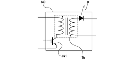
図3は、本発明に係る昇圧回路を説明する図である。この図において昇圧回路140は、例えば好適には昇圧トランスThを用いたフライバック方式のものであるが、昇圧トランスを用いない昇圧チョッパなどの他の方式のものでも構わない。
IGBTやFET等を用いたスイッチング素子sw1は、この昇圧回路140の一次側に設けられ、そのオン期間に流れる電流に基づいて昇圧トランスThに蓄積された磁気エネルギーが、オフ遷移の際にダイオードDを介して解放され、昇圧された電圧を出力するように動作する。このスイッチング素子sw1は、主放電用コンデンサCmの蓄えられた電荷が空に近い状態でデューティ比を高くし充電を行うと、過電流が流れるおそれがある。
IGBTやFET等を用いたスイッチング素子sw1は、この昇圧回路140の一次側に設けられ、そのオン期間に流れる電流に基づいて昇圧トランスThに蓄積された磁気エネルギーが、オフ遷移の際にダイオードDを介して解放され、昇圧された電圧を出力するように動作する。このスイッチング素子sw1は、主放電用コンデンサCmの蓄えられた電荷が空に近い状態でデューティ比を高くし充電を行うと、過電流が流れるおそれがある。
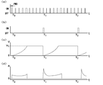
図7は、従来例の点灯装置における充電プロセスを参照して作成した、パルス信号と電流・電圧との関係波形図である。この図は、以下に示す本発明の点灯装置に係る関係波形図を模したものであって、(a)昇圧回路のスイッチング素子sw1に送信されるスイッチゲートアクティブ信号Sc、(b)トリガー電圧生成回路に送信されるトリガーパルス信号St、(c)主放電用コンデンサCmのコンデンサ電圧、(d)スイッチング素子sw1に流れるスイッチング素子電流を同時系列に並べたものである。
なお、波形は模式的な概念図である。特に(a)および(b)については、他の図と同じ時間スケールで波形を描こうとすると細かくなり過ぎて描けないため、判り易いよう故意に粗く描いてある。また(d)については、電流パルス波形のピーク部に関する包絡線として描いてある。図4、図5についても同様である。
この図におけるT0から充電を開始していくと、デューティ比が大きいために大きな電流がスイッチング素子sw1に流れることとなる。そして、放電をするごとに再び充電を開始するが、その際にもスイッチング素子sw1に大きな電流が流れることとなる。
このような不具合を解消するために、本発明者が実施した対策について以下に波形図を用いて説明する。
図4は、本発明の第一の実施形態に係る点灯装置における種々の信号と電流・電圧との関係波形図である。この図は、(a)昇圧回路のスイッチング素子sw1に送信されるスイッチゲートアクティブ信号Sc、(b)トリガー電圧生成回路に送信されるトリガーパルス信号St、(c)主放電用コンデンサCmのコンデンサ電圧、(d)スイッチング素子sw1に流れるスイッチング素子電流を同時系列に並べたものである。
図4の時間的な始点であるT0においては、主放電用コンデンサCmには電荷が蓄えられていない。この状態から、主放電用コンデンサCmに充電していく。
スイッチゲートアクティブ信号Scは、スイッチング素子sw1がオン/オフされる期間に対応するハイレベル/ローレベルを表す信号である。具体的には、スイッチゲートアクティブ信号Scは、スイッチング素子のオン期間中にスイッチング素子に流れる電流が、予め設定された基準過電流値を超えないように、デューティ比を予め設定された初期デューティ比に設定したものである。
すなわち、最初は、スイッチング素子sw1がオンとなる時間は短めに設定される。具体的には初期デューティ比によるパルス幅PW0となる時間だけオンとなる。これは、主放電用コンデンサCmが空に近い状態であるので過電流が回路に流れるのを防止するためである。初期デューティ比は0.1~2.0%であることが好ましい。
なお、ここでは、T0近傍の初期デューティ比を小さく設定するための具体的形態として、パルス頻度を不変として、パルス幅を短くする場合について記載したが、逆にパルス幅を不変として、パルス頻度を低くするようにしてもかまわず、さらにパルス頻度とパルス幅の両方を変化させるようにしても構わない。
初期デューティ比以降のスイッチゲートアクティブ信号Scのデューティ比は時間とともに拡大するように調整される。なお、ここでいう「拡大」とは、少なくとも過電流が流れなくなる程度の電圧に達するまで、初期デューティ比の増加があったことを意味するものであり、途中で一定値に固定されたり、一旦縮小する期間を設けた後に増加されたりしてもよい。過電流が流れる恐れがあるのは充電開始時だからである。ここでいう、過電流が流れなくなる程度の電圧の具体的な値については、基準過電流値、及びコンデンサの目標電圧値よりも低い基準電圧値を予め設定し、充電開始時の電圧から基準電圧値に達するまでの期間を抑制期間として定め、この抑制期間中はスイッチング素子電流が基準過電流値を超えないようにデューティ比を設定する。この基準過電流値、基準電圧値は適宜設定することができる。
また、基準電圧値、又は目標電圧に達するまでにデューティ比を時間とともに拡大するように調整してもよい。
これは、本発明のように例えば10Hz、600Vといった高速かつ高圧でフラッシュ放電を行うためには、効率良く充電する必要があるからである。
すなわち、初期はスイッチング素子sw1に過電流が流れるのを防止するためにデューティ比は抑えておき、主放電用コンデンサCmにある程度電荷が蓄えられて来れば、それに応じてスイッチング素子sw1に流れる電流は低下するため、後半になるほど過電流が流れない程度にバランスをとってデューティ比を増加させることで、充電の速度を上げているのである。
これは、本発明のように例えば10Hz、600Vといった高速かつ高圧でフラッシュ放電を行うためには、効率良く充電する必要があるからである。
すなわち、初期はスイッチング素子sw1に過電流が流れるのを防止するためにデューティ比は抑えておき、主放電用コンデンサCmにある程度電荷が蓄えられて来れば、それに応じてスイッチング素子sw1に流れる電流は低下するため、後半になるほど過電流が流れない程度にバランスをとってデューティ比を増加させることで、充電の速度を上げているのである。
コンデンサ電圧が目標電圧値に到達した後は、デューティ比は概ね一定値に固定される。具体的には、デューティ比は目標電圧値と、実測したコンデンサ電圧との差分に応じて定められる。これは、並列接続された放電抵抗Rdを介した放電による主放電用コンデンサCmの電圧の低下を補償するためである。PWM信号は一定周期で挿入されているので、これによってコンデンサ電圧を一定に保つことができる。
トリガーパルス信号Stがオンになると、トリガー電極7による放電、および主放電電極間でのフラッシュ放電が行われる。
フラッシュ放電が行われると、コンデンサに蓄積された電荷が空の状態になり、充電を再び開始した際には電流が流れやすくなるが、図4のT1に示すように充電を再び開始した際の電流値は従来例よりも低く抑えられることができる。
フラッシュ放電が行われると、コンデンサに蓄積された電荷が空の状態になり、充電を再び開始した際には電流が流れやすくなるが、図4のT1に示すように充電を再び開始した際の電流値は従来例よりも低く抑えられることができる。
図5を用いて、本発明の第2の実施形態について説明する。この図は、図4と同様に(a)昇圧回路のスイッチング素子sw1に送信されるスイッチゲートアクティブ信号Sc、(b)トリガー電圧生成回路に送信されるトリガーパルス信号St、(c)主放電用コンデンサCmのコンデンサ電圧、(d)スイッチング素子sw1に流れるスイッチング素子電流を同時系列に並べたものである。
この実施形態においては、主放電用コンデンサCmの放電時には、トリガーパルス信号Stがオンとなる前に制御回路110が前記スイッチゲートアクティブ信号Scを送信することを停止する。若しくは該スイッチゲートアクティブ信号Scのデューティ比を初期デューティ比より小さい値に設定する。
これは、トリガーパルス信号Stがオンとなった時、すなわち放電時にスイッチング素子sw1に流れる電流をさらに低くするためである。
この効果について図5と図4とを比較する。図4ではT0から充電を開始して、目標電圧に到達した後、デューティ比は概ね一定に固定されたままトリガーパルス信号Stがオンとなっている。この場合、主放電用コンデンサCmの電荷が空の状態でも、スイッチング素子sw1が初期デューティ比を超えるデューティ比でオンしているため、スイッチング素子sw1に少し高い電流が流れてしまう。
再度、図5に戻りこの実施形態についてみると、トリガーパルス信号Stがオンする時刻の前後の期間は避けて、スイッチング素子sw1がオンとなっていることがわかる。これによって、スイッチング素子sw1に流れる電流をさらに低くすることができる。
すなわち、一瞬だけ充電動作稼働率を犠牲にして電流値の低下を優先させているのである。補足するとスイッチング素子をオフにするタイミングを設けても、放電抵抗Rdは、例えば10kΩ以上の大きな値に設定するため、主放電用コンデンサCmの放電による電圧低下は無視できる。
すなわち、一瞬だけ充電動作稼働率を犠牲にして電流値の低下を優先させているのである。補足するとスイッチング素子をオフにするタイミングを設けても、放電抵抗Rdは、例えば10kΩ以上の大きな値に設定するため、主放電用コンデンサCmの放電による電圧低下は無視できる。
このような制御は、制御回路110がスイッチゲートアクティブ信号Scとトリガーパルス信号Stをともに生成して制御することによって実現できる。すなわち、トリガーパルス信号Stが送信されるタイミングは、制御回路110によって定められるため、スイッチゲートアクティブ信号Scはこれを避けるように設定することができるからである。
具体的にスイッチング素子sw1をオフとする期間については、発明者らの研究により、トリガーパルス信号Stがオンとなるタイミングを基点として0.1~2.0msec前までであることが好ましいと分かっている。この期間あれば、主放電用コンデンサCmの充電電圧の低下の影響が少ないからである。したがって、コンデンサの電圧値が目標電圧に達し、最後にスイッチゲートアクティブ信号Scが送信されてから0.1~2.0msec経過した後に、トリガーパルス信号Stを送信する。
フラッシュ放電が完了した後は、再び次の放電に向けて主放電用コンデンサCmに電荷が蓄えられる。この際、主放電の電流が停止した後に初期デューティ比により主放電用コンデンサCmへの供給を再開する。
これは、ショートアーク型フラッシュランプにおいてフラッシュ放電が行われている期間は電気回路的には特殊な遷移状態にあり、このような状態においては動作を行わない方が安全だからである。
これは、ショートアーク型フラッシュランプにおいてフラッシュ放電が行われている期間は電気回路的には特殊な遷移状態にあり、このような状態においては動作を行わない方が安全だからである。
具体的にスイッチング素子sw1をオンとして充電を開始するタイミングは、発明者らの研究により、トリガーパルス信号Stがオンとなったタイミングを基点として0.5~3.0msec経過した後からであることが好ましいと分かっている。この期間あればショートアーク型フラッシュランプにおける一連のフラッシュ放電が完了するからである。
以上により、本発明においては、ショートアーク型フラッシュランプ用の放電ランプ点灯装置において、フラッシュ放電した後に、低いデューティ比から開始して拡大するように充電することにより、素子に流れる電流を低減して、高圧で高速繰り返し的に主放電用コンデンサの充放電を行う際に、回路中の素子の破壊を防止することができる。
1 ショートアーク型フラッシュランプ
2 発光管
5 陰極
6 陽極
7 トリガー電極
11 補助トリガー電極
12 補助トリガー電極
100 放電ランプ点灯装置
110 制御回路
111 スイッチゲートアクティブ信号生成部
112 トリガーパルス信号生成部
120 整流回路
130 PFC回路
140 昇圧回路
150 電流・電圧測定部
160 トリガー電圧生成回路
170 トリガー電圧分配回路
200 商用電源
300 外部インターフェイス
sw1 スイッチング素子
Cm 主放電用コンデンサ
D ダイオード
Rd 放電抵抗
Sc スイッチゲートアクティブ信号
St トリガーパルス信号
Th 昇圧トランス
61 点灯装置
62 フラッシュランプ
63 トリガーソケット
64 出力回路
65 制御回路
69 トリガー出力回路
Claims (3)
- 発光管と、該発光管内の内部に0.5~12.5mmの距離で離間して対向配置された一対の主放電電極とを備えたショートアーク型フラッシュランプを点灯させる放電ランプ点灯装置であって、
前記主放電電極間のフラッシュ放電のための電荷を蓄積する主放電用コンデンサと、スイッチング素子とを有し、該スイッチング素子のオン/オフにより、DC電源の電圧を昇圧して前記主放電用コンデンサに電荷を蓄積する昇圧回路と、
制御回路とを備え、
該制御回路は、前記主放電用コンデンサの充電時に、前記スイッチング素子のオン/オフを規定するスイッチゲートアクティブ信号を前記昇圧回路へ送信し、
前記スイッチゲートアクティブ信号は、前記スイッチング素子のオン期間中に該スイッチング素子に流れる電流が、予め設定された基準過電流値を超えないように、デューティ比を予め設定された初期デューティ比に設定したものであり、
該初期デューティ比は0.1~2.0%であり、
前記制御回路は、前記主放電用コンデンサの充電電圧が目標電圧値よりも低い所定の基準電圧値に達するまでの抑制期間中は、前記デューティ比を、前記スイッチング素子に流れる電流が前記基準電流値を超えない範囲となるよう増加させるものであることを特徴とする放電ランプ点灯装置。 - 前記発光管の内部又は外部にはトリガー電極が設けられ、
前記点灯装置はトリガーパルス信号に応じて前記トリガー電極にトリガー高電圧を供給するためのトリガー電圧生成回路と、前記主放電用コンデンサに並列接続された放電抵抗を備え、
前記制御回路は、前記トリガーパルス信号を前記トリガー電圧生成回路に送信し、
前記主放電用コンデンサの放電時には、前記トリガーパルス信号がオンとなる前に前記制御回路が前記スイッチゲートアクティブ信号を送信することを停止し、若しくは該スイッチゲートアクティブ信号のデューティ比を前記初期デューティ比より小さい値に設定し、
前記主放電電極間での電流が停止した後に、前記初期デューティ比により前記主放電用コンデンサへの電荷の供給を再開することを特徴とする請求項1に記載の放電ランプ点灯装置。 - 前記制御回路は、前記主放電用コンデンサの電圧が目標電圧に達した後、前記トリガーパルス信号がオンとなるまでは、固定された周期のスイッチゲートアクティブ信号を送信して、前記放電抵抗を介した放電による前記主放電用コンデンサの電圧の低下を補償することを特徴とする請求項2に記載の放電ランプ点灯装置。
Applications Claiming Priority (2)
| Application Number | Priority Date | Filing Date | Title |
|---|---|---|---|
| JP2014158769A JP5915946B2 (ja) | 2014-08-04 | 2014-08-04 | 放電ランプ点灯装置 |
| JP2014-158769 | 2014-08-04 |
Publications (1)
| Publication Number | Publication Date |
|---|---|
| WO2016021400A1 true WO2016021400A1 (ja) | 2016-02-11 |
Family
ID=55263672
Family Applications (1)
| Application Number | Title | Priority Date | Filing Date |
|---|---|---|---|
| PCT/JP2015/070683 WO2016021400A1 (ja) | 2014-08-04 | 2015-07-21 | 放電ランプ点灯装置 |
Country Status (2)
| Country | Link |
|---|---|
| JP (1) | JP5915946B2 (ja) |
| WO (1) | WO2016021400A1 (ja) |
Families Citing this family (1)
| Publication number | Priority date | Publication date | Assignee | Title |
|---|---|---|---|---|
| JP7215707B2 (ja) * | 2018-06-21 | 2023-01-31 | 株式会社ユメックス | ショートアーク型フラッシュランプ |
Citations (4)
| Publication number | Priority date | Publication date | Assignee | Title |
|---|---|---|---|---|
| JP2005339987A (ja) * | 2004-05-27 | 2005-12-08 | Pentax Corp | 撮影用発光装置およびそれを備えたカメラ |
| JP2006025597A (ja) * | 2005-07-25 | 2006-01-26 | Konica Minolta Holdings Inc | ストロボ装置 |
| JP2006337880A (ja) * | 2005-06-06 | 2006-12-14 | Panasonic Photo & Lighting Co Ltd | ストロボ装置 |
| JP2008152972A (ja) * | 2006-12-14 | 2008-07-03 | Sony Corp | 発光装置及び発光方法 |
-
2014
- 2014-08-04 JP JP2014158769A patent/JP5915946B2/ja active Active
-
2015
- 2015-07-21 WO PCT/JP2015/070683 patent/WO2016021400A1/ja active Application Filing
Patent Citations (4)
| Publication number | Priority date | Publication date | Assignee | Title |
|---|---|---|---|---|
| JP2005339987A (ja) * | 2004-05-27 | 2005-12-08 | Pentax Corp | 撮影用発光装置およびそれを備えたカメラ |
| JP2006337880A (ja) * | 2005-06-06 | 2006-12-14 | Panasonic Photo & Lighting Co Ltd | ストロボ装置 |
| JP2006025597A (ja) * | 2005-07-25 | 2006-01-26 | Konica Minolta Holdings Inc | ストロボ装置 |
| JP2008152972A (ja) * | 2006-12-14 | 2008-07-03 | Sony Corp | 発光装置及び発光方法 |
Also Published As
| Publication number | Publication date |
|---|---|
| JP2016035864A (ja) | 2016-03-17 |
| JP5915946B2 (ja) | 2016-05-11 |
Similar Documents
| Publication | Publication Date | Title |
|---|---|---|
| US7119502B2 (en) | Flashing discharge tube-use power supply and control method therefor | |
| JP2015019461A (ja) | 蓄電素子の残電圧を放電するための放電回路及び閃光放電ランプ点灯装置 | |
| JP2008178289A (ja) | X線管用の電力供給装置及びそれを動作させるための方法 | |
| JP2005101016A (ja) | 放電灯点灯装置及び車載用照明器具 | |
| WO2016021400A1 (ja) | 放電ランプ点灯装置 | |
| JPH04296834A (ja) | フラッシュランプ及びその点灯回路 | |
| KR20020090298A (ko) | 유전체 배리어 방전 램프 점등장치 | |
| US20110029046A1 (en) | Control circuit for flash lamps or the like | |
| JP2008180919A (ja) | 撮像装置 | |
| JP4970898B2 (ja) | 放電灯点灯装置 | |
| JP5030021B2 (ja) | 高圧放電灯点灯装置及び光源装置並びにその制御方法 | |
| JP4909727B2 (ja) | 半導体装置 | |
| JP3521501B2 (ja) | 高圧放電灯点灯装置 | |
| TWI462645B (zh) | 氙氣燈驅動單元、氙氣燈驅動方法及人工太陽光照射單元 | |
| JP2013110002A (ja) | 放電灯点灯装置および、これを用いた車両用前照灯装置 | |
| JP4984062B2 (ja) | 放電灯点灯装置 | |
| JP2007200757A (ja) | アークランプの点灯回路およびその電圧制御方法 | |
| JP5580677B2 (ja) | 放電灯点灯回路 | |
| JP5360767B2 (ja) | フラッシュランプの点灯装置 | |
| JPH1041081A (ja) | 放電灯点灯装置 | |
| JP6569309B2 (ja) | 放電灯点灯装置 | |
| JPWO2008123274A1 (ja) | 高輝度放電ランプ点灯装置 | |
| JP5569862B2 (ja) | キセノンランプ点灯装置 | |
| JP6417844B2 (ja) | 放電灯点灯装置 | |
| JP2002110312A (ja) | イオン発生装置および電源アダプタ |
Legal Events
| Date | Code | Title | Description |
|---|---|---|---|
| 121 | Ep: the epo has been informed by wipo that ep was designated in this application |
Ref document number: 15830151 Country of ref document: EP Kind code of ref document: A1 |
|
| NENP | Non-entry into the national phase |
Ref country code: DE |
|
| 122 | Ep: pct application non-entry in european phase |
Ref document number: 15830151 Country of ref document: EP Kind code of ref document: A1 |