WO2016017510A1 - 基板処理装置 - Google Patents
基板処理装置 Download PDFInfo
- Publication number
- WO2016017510A1 WO2016017510A1 PCT/JP2015/070905 JP2015070905W WO2016017510A1 WO 2016017510 A1 WO2016017510 A1 WO 2016017510A1 JP 2015070905 W JP2015070905 W JP 2015070905W WO 2016017510 A1 WO2016017510 A1 WO 2016017510A1
- Authority
- WO
- WIPO (PCT)
- Prior art keywords
- substrate
- film
- sputtering
- transport
- path structure
- Prior art date
- Legal status (The legal status is an assumption and is not a legal conclusion. Google has not performed a legal analysis and makes no representation as to the accuracy of the status listed.)
- Ceased
Links
Images





Classifications
-
- C—CHEMISTRY; METALLURGY
- C23—COATING METALLIC MATERIAL; COATING MATERIAL WITH METALLIC MATERIAL; CHEMICAL SURFACE TREATMENT; DIFFUSION TREATMENT OF METALLIC MATERIAL; COATING BY VACUUM EVAPORATION, BY SPUTTERING, BY ION IMPLANTATION OR BY CHEMICAL VAPOUR DEPOSITION, IN GENERAL; INHIBITING CORROSION OF METALLIC MATERIAL OR INCRUSTATION IN GENERAL
- C23C—COATING METALLIC MATERIAL; COATING MATERIAL WITH METALLIC MATERIAL; SURFACE TREATMENT OF METALLIC MATERIAL BY DIFFUSION INTO THE SURFACE, BY CHEMICAL CONVERSION OR SUBSTITUTION; COATING BY VACUUM EVAPORATION, BY SPUTTERING, BY ION IMPLANTATION OR BY CHEMICAL VAPOUR DEPOSITION, IN GENERAL
- C23C14/00—Coating by vacuum evaporation, by sputtering or by ion implantation of the coating forming material
- C23C14/22—Coating by vacuum evaporation, by sputtering or by ion implantation of the coating forming material characterised by the process of coating
- C23C14/34—Sputtering
- C23C14/3464—Sputtering using more than one target
-
- C—CHEMISTRY; METALLURGY
- C23—COATING METALLIC MATERIAL; COATING MATERIAL WITH METALLIC MATERIAL; CHEMICAL SURFACE TREATMENT; DIFFUSION TREATMENT OF METALLIC MATERIAL; COATING BY VACUUM EVAPORATION, BY SPUTTERING, BY ION IMPLANTATION OR BY CHEMICAL VAPOUR DEPOSITION, IN GENERAL; INHIBITING CORROSION OF METALLIC MATERIAL OR INCRUSTATION IN GENERAL
- C23C—COATING METALLIC MATERIAL; COATING MATERIAL WITH METALLIC MATERIAL; SURFACE TREATMENT OF METALLIC MATERIAL BY DIFFUSION INTO THE SURFACE, BY CHEMICAL CONVERSION OR SUBSTITUTION; COATING BY VACUUM EVAPORATION, BY SPUTTERING, BY ION IMPLANTATION OR BY CHEMICAL VAPOUR DEPOSITION, IN GENERAL
- C23C14/00—Coating by vacuum evaporation, by sputtering or by ion implantation of the coating forming material
- C23C14/02—Pretreatment of the material to be coated
- C23C14/021—Cleaning or etching treatments
- C23C14/022—Cleaning or etching treatments by means of bombardment with energetic particles or radiation
-
- C—CHEMISTRY; METALLURGY
- C23—COATING METALLIC MATERIAL; COATING MATERIAL WITH METALLIC MATERIAL; CHEMICAL SURFACE TREATMENT; DIFFUSION TREATMENT OF METALLIC MATERIAL; COATING BY VACUUM EVAPORATION, BY SPUTTERING, BY ION IMPLANTATION OR BY CHEMICAL VAPOUR DEPOSITION, IN GENERAL; INHIBITING CORROSION OF METALLIC MATERIAL OR INCRUSTATION IN GENERAL
- C23C—COATING METALLIC MATERIAL; COATING MATERIAL WITH METALLIC MATERIAL; SURFACE TREATMENT OF METALLIC MATERIAL BY DIFFUSION INTO THE SURFACE, BY CHEMICAL CONVERSION OR SUBSTITUTION; COATING BY VACUUM EVAPORATION, BY SPUTTERING, BY ION IMPLANTATION OR BY CHEMICAL VAPOUR DEPOSITION, IN GENERAL
- C23C14/00—Coating by vacuum evaporation, by sputtering or by ion implantation of the coating forming material
- C23C14/22—Coating by vacuum evaporation, by sputtering or by ion implantation of the coating forming material characterised by the process of coating
- C23C14/34—Sputtering
- C23C14/3435—Applying energy to the substrate during sputtering
- C23C14/345—Applying energy to the substrate during sputtering using substrate bias
-
- C—CHEMISTRY; METALLURGY
- C23—COATING METALLIC MATERIAL; COATING MATERIAL WITH METALLIC MATERIAL; CHEMICAL SURFACE TREATMENT; DIFFUSION TREATMENT OF METALLIC MATERIAL; COATING BY VACUUM EVAPORATION, BY SPUTTERING, BY ION IMPLANTATION OR BY CHEMICAL VAPOUR DEPOSITION, IN GENERAL; INHIBITING CORROSION OF METALLIC MATERIAL OR INCRUSTATION IN GENERAL
- C23C—COATING METALLIC MATERIAL; COATING MATERIAL WITH METALLIC MATERIAL; SURFACE TREATMENT OF METALLIC MATERIAL BY DIFFUSION INTO THE SURFACE, BY CHEMICAL CONVERSION OR SUBSTITUTION; COATING BY VACUUM EVAPORATION, BY SPUTTERING, BY ION IMPLANTATION OR BY CHEMICAL VAPOUR DEPOSITION, IN GENERAL
- C23C14/00—Coating by vacuum evaporation, by sputtering or by ion implantation of the coating forming material
- C23C14/22—Coating by vacuum evaporation, by sputtering or by ion implantation of the coating forming material characterised by the process of coating
- C23C14/50—Substrate holders
-
- C—CHEMISTRY; METALLURGY
- C23—COATING METALLIC MATERIAL; COATING MATERIAL WITH METALLIC MATERIAL; CHEMICAL SURFACE TREATMENT; DIFFUSION TREATMENT OF METALLIC MATERIAL; COATING BY VACUUM EVAPORATION, BY SPUTTERING, BY ION IMPLANTATION OR BY CHEMICAL VAPOUR DEPOSITION, IN GENERAL; INHIBITING CORROSION OF METALLIC MATERIAL OR INCRUSTATION IN GENERAL
- C23C—COATING METALLIC MATERIAL; COATING MATERIAL WITH METALLIC MATERIAL; SURFACE TREATMENT OF METALLIC MATERIAL BY DIFFUSION INTO THE SURFACE, BY CHEMICAL CONVERSION OR SUBSTITUTION; COATING BY VACUUM EVAPORATION, BY SPUTTERING, BY ION IMPLANTATION OR BY CHEMICAL VAPOUR DEPOSITION, IN GENERAL
- C23C14/00—Coating by vacuum evaporation, by sputtering or by ion implantation of the coating forming material
- C23C14/22—Coating by vacuum evaporation, by sputtering or by ion implantation of the coating forming material characterised by the process of coating
- C23C14/54—Controlling or regulating the coating process
- C23C14/541—Heating or cooling of the substrates
-
- C—CHEMISTRY; METALLURGY
- C23—COATING METALLIC MATERIAL; COATING MATERIAL WITH METALLIC MATERIAL; CHEMICAL SURFACE TREATMENT; DIFFUSION TREATMENT OF METALLIC MATERIAL; COATING BY VACUUM EVAPORATION, BY SPUTTERING, BY ION IMPLANTATION OR BY CHEMICAL VAPOUR DEPOSITION, IN GENERAL; INHIBITING CORROSION OF METALLIC MATERIAL OR INCRUSTATION IN GENERAL
- C23C—COATING METALLIC MATERIAL; COATING MATERIAL WITH METALLIC MATERIAL; SURFACE TREATMENT OF METALLIC MATERIAL BY DIFFUSION INTO THE SURFACE, BY CHEMICAL CONVERSION OR SUBSTITUTION; COATING BY VACUUM EVAPORATION, BY SPUTTERING, BY ION IMPLANTATION OR BY CHEMICAL VAPOUR DEPOSITION, IN GENERAL
- C23C14/00—Coating by vacuum evaporation, by sputtering or by ion implantation of the coating forming material
- C23C14/22—Coating by vacuum evaporation, by sputtering or by ion implantation of the coating forming material characterised by the process of coating
- C23C14/56—Apparatus specially adapted for continuous coating; Arrangements for maintaining the vacuum, e.g. vacuum locks
- C23C14/568—Transferring the substrates through a series of coating stations
-
- H—ELECTRICITY
- H01—ELECTRIC ELEMENTS
- H01J—ELECTRIC DISCHARGE TUBES OR DISCHARGE LAMPS
- H01J37/00—Discharge tubes with provision for introducing objects or material to be exposed to the discharge, e.g. for the purpose of examination or processing thereof
- H01J37/32—Gas-filled discharge tubes
- H01J37/32431—Constructional details of the reactor
- H01J37/32733—Means for moving the material to be treated
- H01J37/32752—Means for moving the material to be treated for moving the material across the discharge
-
- H—ELECTRICITY
- H01—ELECTRIC ELEMENTS
- H01J—ELECTRIC DISCHARGE TUBES OR DISCHARGE LAMPS
- H01J37/00—Discharge tubes with provision for introducing objects or material to be exposed to the discharge, e.g. for the purpose of examination or processing thereof
- H01J37/32—Gas-filled discharge tubes
- H01J37/34—Gas-filled discharge tubes operating with cathodic sputtering
- H01J37/3411—Constructional aspects of the reactor
- H01J37/3414—Targets
- H01J37/3417—Arrangements
-
- H—ELECTRICITY
- H05—ELECTRIC TECHNIQUES NOT OTHERWISE PROVIDED FOR
- H05K—PRINTED CIRCUITS; CASINGS OR CONSTRUCTIONAL DETAILS OF ELECTRIC APPARATUS; MANUFACTURE OF ASSEMBLAGES OF ELECTRICAL COMPONENTS
- H05K3/00—Apparatus or processes for manufacturing printed circuits
- H05K3/10—Apparatus or processes for manufacturing printed circuits in which conductive material is applied to the insulating support in such a manner as to form the desired conductive pattern
- H05K3/14—Apparatus or processes for manufacturing printed circuits in which conductive material is applied to the insulating support in such a manner as to form the desired conductive pattern using spraying techniques to apply the conductive material, e.g. vapour evaporation
- H05K3/16—Apparatus or processes for manufacturing printed circuits in which conductive material is applied to the insulating support in such a manner as to form the desired conductive pattern using spraying techniques to apply the conductive material, e.g. vapour evaporation by cathodic sputtering
-
- H—ELECTRICITY
- H10—SEMICONDUCTOR DEVICES; ELECTRIC SOLID-STATE DEVICES NOT OTHERWISE PROVIDED FOR
- H10P—GENERIC PROCESSES OR APPARATUS FOR THE MANUFACTURE OR TREATMENT OF DEVICES COVERED BY CLASS H10
- H10P72/00—Handling or holding of wafers, substrates or devices during manufacture or treatment thereof
- H10P72/04—Apparatus for manufacture or treatment
- H10P72/0431—Apparatus for thermal treatment
- H10P72/0434—Apparatus for thermal treatment mainly by convection
-
- H—ELECTRICITY
- H10—SEMICONDUCTOR DEVICES; ELECTRIC SOLID-STATE DEVICES NOT OTHERWISE PROVIDED FOR
- H10P—GENERIC PROCESSES OR APPARATUS FOR THE MANUFACTURE OR TREATMENT OF DEVICES COVERED BY CLASS H10
- H10P72/00—Handling or holding of wafers, substrates or devices during manufacture or treatment thereof
- H10P72/04—Apparatus for manufacture or treatment
- H10P72/0451—Apparatus for manufacturing or treating in a plurality of work-stations
- H10P72/0452—Apparatus for manufacturing or treating in a plurality of work-stations characterised by the layout of the process chambers
- H10P72/0456—Apparatus for manufacturing or treating in a plurality of work-stations characterised by the layout of the process chambers in-line arrangement
-
- H—ELECTRICITY
- H10—SEMICONDUCTOR DEVICES; ELECTRIC SOLID-STATE DEVICES NOT OTHERWISE PROVIDED FOR
- H10P—GENERIC PROCESSES OR APPARATUS FOR THE MANUFACTURE OR TREATMENT OF DEVICES COVERED BY CLASS H10
- H10P72/00—Handling or holding of wafers, substrates or devices during manufacture or treatment thereof
- H10P72/30—Handling or holding of wafers, substrates or devices during manufacture or treatment thereof for conveying, e.g. between different workstations
- H10P72/32—Handling or holding of wafers, substrates or devices during manufacture or treatment thereof for conveying, e.g. between different workstations between different workstations
- H10P72/3202—Mechanical details, e.g. rollers or belts
-
- H—ELECTRICITY
- H10—SEMICONDUCTOR DEVICES; ELECTRIC SOLID-STATE DEVICES NOT OTHERWISE PROVIDED FOR
- H10P—GENERIC PROCESSES OR APPARATUS FOR THE MANUFACTURE OR TREATMENT OF DEVICES COVERED BY CLASS H10
- H10P72/00—Handling or holding of wafers, substrates or devices during manufacture or treatment thereof
- H10P72/30—Handling or holding of wafers, substrates or devices during manufacture or treatment thereof for conveying, e.g. between different workstations
- H10P72/32—Handling or holding of wafers, substrates or devices during manufacture or treatment thereof for conveying, e.g. between different workstations between different workstations
- H10P72/3206—Handling or holding of wafers, substrates or devices during manufacture or treatment thereof for conveying, e.g. between different workstations between different workstations the substrate being handled substantially vertically
-
- H—ELECTRICITY
- H10—SEMICONDUCTOR DEVICES; ELECTRIC SOLID-STATE DEVICES NOT OTHERWISE PROVIDED FOR
- H10P—GENERIC PROCESSES OR APPARATUS FOR THE MANUFACTURE OR TREATMENT OF DEVICES COVERED BY CLASS H10
- H10P72/00—Handling or holding of wafers, substrates or devices during manufacture or treatment thereof
- H10P72/30—Handling or holding of wafers, substrates or devices during manufacture or treatment thereof for conveying, e.g. between different workstations
- H10P72/33—Handling or holding of wafers, substrates or devices during manufacture or treatment thereof for conveying, e.g. between different workstations into and out of processing chamber
- H10P72/3314—Continuous loading and unloading into and out of a processing chamber, e.g. transporting belts within processing chambers
-
- H—ELECTRICITY
- H10—SEMICONDUCTOR DEVICES; ELECTRIC SOLID-STATE DEVICES NOT OTHERWISE PROVIDED FOR
- H10P—GENERIC PROCESSES OR APPARATUS FOR THE MANUFACTURE OR TREATMENT OF DEVICES COVERED BY CLASS H10
- H10P72/00—Handling or holding of wafers, substrates or devices during manufacture or treatment thereof
- H10P72/70—Handling or holding of wafers, substrates or devices during manufacture or treatment thereof for supporting or gripping
- H10P72/72—Handling or holding of wafers, substrates or devices during manufacture or treatment thereof for supporting or gripping using electrostatic chucks
-
- H—ELECTRICITY
- H05—ELECTRIC TECHNIQUES NOT OTHERWISE PROVIDED FOR
- H05K—PRINTED CIRCUITS; CASINGS OR CONSTRUCTIONAL DETAILS OF ELECTRIC APPARATUS; MANUFACTURE OF ASSEMBLAGES OF ELECTRICAL COMPONENTS
- H05K2201/00—Indexing scheme relating to printed circuits covered by H05K1/00
- H05K2201/01—Dielectrics
- H05K2201/0137—Materials
- H05K2201/0145—Polyester, e.g. polyethylene terephthalate [PET], polyethylene naphthalate [PEN]
-
- H—ELECTRICITY
- H05—ELECTRIC TECHNIQUES NOT OTHERWISE PROVIDED FOR
- H05K—PRINTED CIRCUITS; CASINGS OR CONSTRUCTIONAL DETAILS OF ELECTRIC APPARATUS; MANUFACTURE OF ASSEMBLAGES OF ELECTRICAL COMPONENTS
- H05K2201/00—Indexing scheme relating to printed circuits covered by H05K1/00
- H05K2201/01—Dielectrics
- H05K2201/0137—Materials
- H05K2201/0154—Polyimide
-
- H—ELECTRICITY
- H05—ELECTRIC TECHNIQUES NOT OTHERWISE PROVIDED FOR
- H05K—PRINTED CIRCUITS; CASINGS OR CONSTRUCTIONAL DETAILS OF ELECTRIC APPARATUS; MANUFACTURE OF ASSEMBLAGES OF ELECTRICAL COMPONENTS
- H05K2201/00—Indexing scheme relating to printed circuits covered by H05K1/00
- H05K2201/01—Dielectrics
- H05K2201/0137—Materials
- H05K2201/0158—Polyalkene or polyolefin, e.g. polyethylene [PE], polypropylene [PP]
Definitions
- the present invention relates to a substrate processing apparatus for processing both surfaces of a substrate.
- a thin substrate such as a film-like substrate has lower heat resistance than a glass substrate or the like that has been widely used conventionally.
- the temperature of the substrate surface rises when high-energy sputtered particles reach the surface of the substrate. If the substrate surface temperature exceeds the allowable temperature of the substrate material, the substrate may be deformed. Therefore, when forming a film on a thin substrate, the film is formed within a temperature range that does not exceed the allowable temperature of the substrate material. There is a need.
- double-sided film formation may be performed in which film formation is performed on both surfaces of a substrate. At this time, if both sides of the substrate are simultaneously formed, the substrate temperature is likely to rise as compared to single-sided film formation. Therefore, it is necessary to form the film on each side in two steps.
- An example of an apparatus that forms a film on each side of a substrate is a device that changes the direction of the substrate by a transfer robot. For example, when film formation on one film formation surface of a substrate is completed, the transfer robot rotates the substrate and carries it into a film formation apparatus that forms a film on the other film formation surface of the substrate.
- a substrate processing apparatus provided with a transfer robot is described in Patent Document 1, for example.
- a rotation mechanism for rotating a substrate such as a transfer robot
- the rotation mechanism is responsible for rotation of the substrate and transfer to a plurality of substrate processing chambers.
- the operation time of the rotating mechanism becomes a bottleneck that limits the production amount. Therefore, there is a demand for a substrate processing apparatus that can form a thin film on both sides of a substrate, which can further increase production efficiency.
- Such a problem is not limited to an apparatus that uses a thin substrate as a substrate processing target, but is generally common to substrate processing apparatuses that require cooling of the substrate.
- An object of the present invention is to provide a substrate processing apparatus capable of increasing the production efficiency in double-sided film formation.
- One embodiment of the present invention is a substrate processing apparatus.
- the substrate processing apparatus is provided along a sputtering chamber, two targets for forming a thin film by sputtering on two film formation surfaces of the substrate, and a transport path provided in the sputtering chamber.
- a transport mechanism for transporting the substrate wherein one of the two targets is disposed in the front stage of the substrate transport direction so as to face one of the two film formation surfaces of the substrate.
- the other side of the two targets is disposed on one side of the substrate, and the other side of the transport path is opposite to the other of the two film formation surfaces of the substrate in the subsequent stage in the transport direction of the substrate. Placed in the direction.
- a thin film is formed on one film formation surface of the substrate facing the target by one target arranged in the previous stage in the substrate transport direction. Furthermore, a thin film is formed on the other film-forming surface of the substrate facing the target by the other target disposed in the subsequent stage in the substrate transport direction. For this reason, since it can form into a film one side at a time, without rotating a board
- the sputter chamber is one of a first sputter chamber and a second sputter chamber provided side by side in a front stage and a rear stage in the transport direction, and the two sputter chambers provided in the first sputter chamber.
- the target and the two targets provided in the second sputtering chamber are disposed at different positions in the transport direction, and are alternately disposed on one side and the other side of the transport path. Is preferred.
- the four targets including the two targets of the first sputtering chamber at the front stage and the two targets of the second sputtering chamber at the rear stage are alternately arranged on one side and the other side of the transport path. . For this reason, even when film formation is performed twice on both surfaces of the substrate, film formation can be performed on each side without rotating the substrate, so that the production efficiency in the double-side film formation can be increased.
- the substrate processing apparatus is provided in a reverse sputtering chamber for cleaning two film formation surfaces of the substrate by transferring the substrate prior to transfer to the sputtering chamber, and in the reverse sputtering chamber.
- Two bias electrodes to which a bias voltage is applied, and the two bias electrodes are arranged separately in a front stage and a rear stage in the transport direction, and are divided into one side and the other side of the transport path. are preferably arranged.
- the substrate processing apparatus includes a return path structure including the sputter chamber, a substrate mounting portion that is disposed on a carry-out side of the return path structure, and that mounts the substrate on a substrate holding portion, and is mounted on the substrate holding portion.
- An outward path structure that transports the substrate from the exit side of the return path structure to the entrance side of the return path structure, and the outbound path structure heats the substrate at a preset upper limit temperature or less. It is preferable that the heating part to be included.
- the substrate can be heated by the heating unit provided in the forward path structure while the substrate mounted on the substrate holding part is transported from the carry-out side of the return path structure to the carry-in side.
- the heating unit heats the substrate at a temperature not higher than a preset upper limit temperature, the substrate can be degassed while preventing deformation of the substrate or the like depending on the setting of the upper limit temperature.
- the transport mechanism includes a control device that controls transport of the substrate to the forward path structure and transport of the substrate from the forward path structure to the return path structure. It is preferable to carry in the substrate before film formation from the forward path structure to the return path structure in accordance with the unloading of the substrate from the return path structure.
- the board in accordance with the carry-out of the substrate from the return path structure, the board is loaded into the return path structure. For this reason, since the board
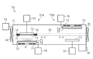
- the side view which shows schematic structure of one Embodiment of a substrate processing apparatus.
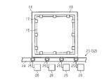
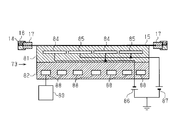
- the schematic diagram of the conveyance mechanism in the substrate processing apparatus of FIG. The top view which shows schematic structure of the substrate processing apparatus of FIG.
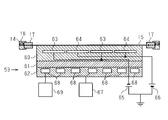
- the schematic diagram which shows the structure of the reverse sputtering apparatus in the substrate processing apparatus of FIG. Sectional drawing which shows typically the electrostatic chuck provided in the reverse sputtering apparatus of FIG.
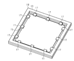
- the front view which shows the board
- the substrate processing apparatus is exemplified as an apparatus that forms, on both sides of a substrate on which an electronic component is mounted, an adhesion layer as a base of wiring and a seed layer for forming wiring by plating by sputtering.
- substrate used as film-forming object is a film-like board
- the film substrate is mainly composed of resin.
- resin for example, acrylic resin, polyamide resin, melamine resin, polyimide resin, polyester resin, cellulose, and copolymer resins thereof are used.
- organic natural compounds such as gelatin and casein are used as the film substrate material.
- the material for forming the film substrate includes polyester, polyethylene terephthalate, polybutylene terephthalate, polymethylene methacrylate, acrylic, polycarbonate, polystyrene, triacetate, polyvinyl alcohol, polyvinyl chloride, polyvinylidene chloride, polyethylene, and ethylene-vinyl acetate.
- Copolymers, polyvinyl butyral, metal ion cross-linked ethylene-methacrylic acid copolymers, polyurethane, cellophane and the like are used.
- it is preferable that any of polyethylene terephthalate, polycarbonate, polymethylene methacrylate, and triacetate is used as a film substrate forming material.
- a film substrate having a thickness of 1 mm or less is preferably used, and a film substrate having a thickness of 100 ⁇ m or less is more preferably used. Further, for example, the film substrate has a side length (width and height in plan view) of 500 mm to 600 mm.
- the substrate processing apparatus 10 includes a substrate mounting unit 11 and a first substrate lifting unit 13.
- the substrate mounting unit 11 is a device that mounts the film substrate 15 before film formation on the substrate holding unit 14 and removes the film substrate 15 after film formation from the substrate holding unit 14.
- the substrate mounting unit 11 and the first substrate lifting unit 13 are controlled by the control device 12.
- the substrate holding part 14 includes a frame 16 and a substrate fixture 17 provided on the inner peripheral surface of the frame 16.
- the substrate fixture 17 is made of a magnet, and a plurality of substrate fixtures 17 are provided on the four sides of the frame body 16.
- the frame 16 is composed of a first frame 16a and a second frame 16b.
- first frame body 16a and the second frame body 16b On the inner peripheral surface side of the first frame body 16a and the second frame body 16b, groove-shaped fitted portions 16c and 16d are formed.
- the first frame body 16a and the second frame body 16b are fixed to each other by a fixture or the like (not shown).
- the magnet 16e is embed
- the substrate fixture 17 includes a pair of fixing pieces 17a and 17b.
- substrate fixture 17 is equipped with the groove part 17c in the end. The edge of the film substrate 15 is inserted into the groove portion 17c.
- the groove portion 17c can be omitted depending on the thickness of the film substrate 15.
- the film substrate 15 is mounted on the substrate holding portion 14, for example, the film substrate 15 is attached to the second frame in a state in which the fixing piece 17b of the substrate fixture 17 is disposed on the fitted portion 16d of the second frame body 16b. It arrange
- the fixed piece 17a is arrange
- the fixed piece 17a is attracted toward the first frame 16a by the magnetic force of the magnet 16e.
- positioned the fixed piece 17a is piled up on the 2nd frame 16b which mounted the film board
- the film substrate 15 is fixed to the frame 16 via the substrate fixture 17.
- the film substrate 15 mounted on the substrate holding unit 14 by the substrate mounting unit 11 is lifted by the first substrate lifting unit 13 and is provided in the forward structure provided vertically above the substrate mounting unit 11. It is conveyed into the body 21.
- the forward path structure 21 includes a long casing 21a and an outbound path 23 provided in the casing 21a.
- the forward transfer path 23 transfers the film substrate 15 mounted on the substrate holding unit 14 from the first substrate lifting unit 13 toward the second substrate lifting unit 30 provided on the side opposite to the first substrate lifting unit 13. To do.
- the forward conveyance path 23 includes a conveyance rail 24 and a plurality of conveyance rollers 25.
- the transport roller 25 is provided in a state where it can rotate with respect to the transport rail 24.
- the transport roller 25 is driven by a drive source such as a transport motor 26.
- the transport motor 26 is controlled by the control device 12.
- the transport rail 24, the transport roller 25, the transport motor 26, and the control device 12 constitute a transport mechanism that transports the film substrate 15.
- a plurality of heaters 31 are provided in a part of the casing 21a in the longitudinal direction.
- the heaters 31 are provided on both sides of the outbound path 23 and heat the film substrate 15 transported along the outbound path 23 from both sides.
- the plurality of heaters 31 are arranged along the longitudinal direction of the housing 21a. Since the film substrate 15 is hygroscopic in terms of material properties, the film substrate 15 is degassed by being continuously heated by the plurality of heaters 31.
- the heater 31 is composed of, for example, a sheathed heater in which a heating wire is housed in a metal pipe via an insulator, and the temperature is adjusted by the control device 12 to an upper limit temperature Tmax or less that can prevent deformation of the film substrate 15.
- This upper limit temperature Tmax is set according to the material of the film substrate 15.
- the number of heaters 31 is adjusted so that the heating time in the forward path structure 21 is equal to or longer than the time required for degassing the film substrate 15.
- the degassed film substrate 15 is sequentially lowered by the second substrate elevating unit 30 controlled by the control device 12 and conveyed to the return path structure 22 provided below the forward path structure 21 in the vertical direction.
- the return path structure 22 includes a reverse sputtering device 50, a first sputtering device 70, and a second sputtering device 90.
- the reverse sputtering apparatus 50 is an apparatus that performs reverse sputtering for cleaning both surfaces of the film substrate 15.
- the first sputtering apparatus 70 is an apparatus that forms an adhesion layer on the film substrate 15, and the second sputtering apparatus 90 is an apparatus that forms a seed layer on the adhesion layer.
- a carry-in chamber 35 having a carry-in port 35a (see FIG. 5) and a first preliminary chamber 36 are provided.
- a second preliminary chamber 37 and a carry-out chamber 38 having a carry-out port 38a are provided between the second sputtering apparatus 90 and the substrate mounting portion 11.
- a return conveyance path 32 is provided in the carry-in chamber 35, the first preliminary chamber 36, the reverse sputtering device 50, the first sputtering device 70, the second sputtering device 90, the second preliminary chamber 37, and the carry-out chamber 38.
- the return path 32 is provided with a transport rail 24 and a transport roller 25 in the same manner as the forward path 23.
- the transport roller 25 is connected to the transport motor 26.
- the transport motor 26 of the return path 32 is also controlled by the control device 12.
- the film substrate 15 is conveyed linearly along the return path transport path 32 in the return path structure 22 from the second substrate elevating unit 30 toward the substrate mounting unit 11.
- Gate valves 41 to 43 are provided at the carry-in port 35 a of the carry-in chamber 35, between the carry-in chamber 35 and the first spare chamber 36, and at the outlet of the first spare chamber 36.
- the carry-in chamber 35 and the first preliminary chamber 36 are adjusted to a predetermined pressure range by an exhaust unit (not shown).
- Gate valves 46 to 48 are provided between the second sputtering apparatus 90 and the second preliminary chamber 37, between the second preliminary chamber 37 and the carry-out chamber 38, and at the outlet of the carry-out chamber 38.
- the second preliminary chamber 37 and the carry-out chamber 38 are adjusted to a predetermined pressure range by an exhaust unit (not shown).
- the heaters 40 are provided on both sides facing each other across the return path 32 (see FIG. 5).
- the heater 40 is composed of a sheathed heater, for example, and the temperature is adjusted by the control device 12 to be equal to or lower than the upper limit temperature described above.
- the final degassing process before film formation is performed by heating both surfaces of the film substrate 15.
- the heating temperature set for the heater 40 of the first preliminary chamber 36 and the heating temperature set for the heater 31 of the forward path structure 21 may be the same or different from each other.
- the heating temperature set for the heater 40 of the first preliminary chamber 36 is higher than the heating temperature set for the heater 31 of the forward path structure 21, the temperature of the film substrate 15 rises to just before film formation. In order to continue, the adsorption
- the reverse sputtering apparatus 50 includes two electrostatic chucks 53.
- the electrostatic chuck 53 has a bias electrode to which high frequency power is supplied.
- the reverse sputtering apparatus 50 generates plasma including positive ions of electrons and sputtering gas in the internal space of the reverse sputtering chamber 51 (see FIG. 6), and applies a bias voltage to the electrostatic chuck 53 to thereby generate plasma in the plasma.
- the positive ions are drawn into the surface of the film substrate 15 to remove the deposits and the like on the film substrate 15.
- One electrostatic chuck 53 is provided in the front stage in the substrate transport direction, which is the transport direction of the film substrate 15, and the other electrostatic chuck 53 is provided in the rear stage in the substrate transport direction.
- the front-stage electrostatic chuck 53 is provided on the left side as viewed from the inlet side of the reverse sputtering apparatus 50, and the rear-stage electrostatic chuck 53 is provided on the right side as viewed from the inlet side.
- the first sputtering apparatus 70 includes two pairs of a first cathode unit 72 having a target and an electrostatic chuck 73.
- the target has, for example, titanium as a main component.
- One pair of the first cathode unit 72 and the electrostatic chuck 73 is provided at the front stage in the substrate transport direction, and the other pair of the first cathode unit 72 and the electrostatic chuck 73 is provided at the rear stage in the substrate transport direction. Yes.
- the two pairs of the first cathode unit 72 and the electrostatic chuck 73 are provided at positions that do not overlap in the substrate transport direction.
- the first cathode unit 72 at the front stage and the first cathode unit 72 at the rear stage are provided on different sides with respect to the return path 32. That is, the two first cathode units 72 are provided at different positions in the transport direction of the film substrate 15 and different positions in a direction orthogonal to the transport direction.
- the second sputtering apparatus 90 includes gate valves 45 and 46 between the first sputtering apparatus 70 and the second preliminary chamber 37.
- the second sputtering apparatus 90 includes two pairs of a second cathode unit 92 and an electrostatic chuck 93 having a target.
- the target has, for example, copper as a main component.
- One pair of the second cathode unit 92 and the electrostatic chuck 93 is provided in the front stage in the substrate transport direction, and the other pair of the second cathode unit 92 and the electrostatic chuck 93 is provided in the rear stage in the substrate transport direction. Yes.
- the two pairs of second cathode units 92 and electrostatic chucks 93 are provided at positions that do not overlap in the substrate transport direction.
- the front-stage second cathode unit 92 and the rear-stage second cathode unit 92 are provided on different sides of the return path transport path 32. That is, the two second cathode units 92 are provided at different positions in the transport direction of the film substrate 15 and different positions in the direction orthogonal to the transport direction.
- the two first cathode units 72 of the first sputtering apparatus 70 and the two second cathode units 92 of the second sputtering apparatus 90 are alternately arranged on one side and the other side in the transport direction of the film substrate 15. Has been placed.
- the electrostatic chucks 53 are alternately arranged on the sides in the transport direction.
- the film substrate 15 passes through the reverse sputtering apparatus 50, the first sputtering apparatus 70, and the second sputtering apparatus 90 in a state where the film substrate 15 stands vertically on the conveyance rail 24 by the control of the conveyance motor 26 by the control apparatus 12.
- the film substrate 15 is reverse-sputtered in the order of the right side surface 15 a that is one film formation surface and the left side surface 15 b that is the other film formation surface when viewed from the inlet side of the reverse sputtering apparatus 50.
- the first sputtering apparatus 70 thin films are formed in order of the right side surface 15a and the left side surface 15b.
- the second sputtering apparatus 90 thin films are formed in order of the right side surface 15a and the left side surface 15b.
- the film substrate 15 transported through the reverse sputtering apparatus 50, the first sputtering apparatus 70, and the second sputtering apparatus 90 is subjected to substrate processing alternately in the order of the right side surface 15a and the left side surface 15b. For this reason, after processing one film-forming surface, while processing the other film-forming surface continuously, one film-forming surface on the opposite side is cooled.
- the return conveyance path 32 extends linearly between the gate valve 43 provided on the inlet side and the gate valve 44 provided on the outlet side. ing.
- the reverse sputtering chamber 51 is connected to an exhaust unit 56 that exhausts the internal space and a sputtering gas supply unit 57 that supplies a sputtering gas containing argon to the internal space.
- a sputtering gas any of nitrogen gas, oxygen gas, and hydrogen gas may be used in addition to argon, or a gas in which at least two of these four kinds of gases including argon are mixed may be used.
- the exhaust unit 56 and the sputtering gas supply unit 57 are controlled by the control device 12.
- the reverse sputtering apparatus 50 includes a reverse sputtering unit 50A at the front stage and a reverse sputtering part 50B at the rear stage. Since the upstream reverse sputtering unit 50A and the downstream reverse sputtering unit 50B have the same configuration, only the configuration of the upstream reverse sputtering unit 50A will be described.
- the reverse sputtering unit 50 ⁇ / b> A has one electrostatic chuck 53.
- the front stage electrostatic chuck 53 is provided on the left side when viewed from the entrance side, on both sides of the return path 32. Further, the latter stage electrostatic chuck 53 is provided on the right side when viewed from the entrance side of the return path conveyance path 32.
- the electrostatic chuck 53 attracts the film substrate 15 by a force generated between the electrostatic chuck 53 and the film substrate 15. Further, the film substrate 15 is cooled by absorbing the heat of the film substrate 15 whose temperature has been increased by reverse sputtering.
- the electrostatic chuck 53 is connected to the electrostatic chuck displacing portion 54, and the electrostatic chuck 53 is in contact with the film substrate 15 on the return path 32 and in contact with the film substrate 15 on the return path 32. Displace between non-contact positions.
- the electrostatic chuck 53 has a laminated body in which an insulating plate 60, a copper plate 61, and a bias electrode 62 are laminated.
- the insulating plate 60 provided in the uppermost layer includes a base material such as ceramics such as aluminum oxide or a resin such as polyimide, and is formed in a rectangular shape and a plate shape.
- a plurality of positive electrodes 63 and a plurality of negative electrodes 64 are embedded in the insulating plate 60.
- the positive electrode 63 and the negative electrode 64 are formed in an elongated shape, and are alternately arranged with a space therebetween.
- a positive electrode power supply 65 is electrically connected to the positive electrode 63, and a negative electrode power supply 66 is electrically connected to the negative electrode 64.
- the positive electrode power supply 65 applies a relatively positive voltage to the positive electrode 63.
- the negative electrode power supply 66 applies a relatively negative voltage to the negative electrode 64.
- the bias electrode 62 is connected to a high frequency power source 67 for bias.
- High frequency power is supplied to the bias electrode 62 by a high frequency power supply 67 for bias.
- the high-frequency power preferably has a frequency of 1 MHz to 6 MHz, for example.
- the high frequency power source 67 for bias may be configured to supply a high frequency power having a relatively high frequency and a high frequency power having a relatively low frequency. In this case, it is preferable to supply high frequency power of 13 MHz to 28 MHz and high frequency power of 100 kHz to 1 MHz.
- the bias electrode 62 is formed with a refrigerant passage 68 through which the refrigerant passes.
- the refrigerant passage 68 has, for example, a bent shape in which the inside of the plate-like bias electrode 62 is bent a plurality of times.
- a refrigerant circulation portion 69 is connected to the refrigerant passage 68, and the refrigerant circulation portion 69 circulates the refrigerant in the refrigerant passage 68.
- a cooling liquid such as cooling water, a fluorine-based solution, and an ethylene glycol solution, or a cooling gas such as helium gas or argon gas is used.
- the transfer motor 26 is driven to place the film substrate 15 at a predetermined position. Further, the electrostatic chuck displacement portion 54 is driven, and the electrostatic chuck 53 is displaced to the contact position. Further, power is supplied from the positive electrode power supply 65 and the negative electrode power supply 66 to the positive electrode 63 and the negative electrode 64, and the film substrate 15 is attracted to the insulating plate 60.
- the exhaust unit 56 is driven and the sputtering gas is supplied to the plasma generation space S, whereby the inside of the reverse sputtering chamber 51 is adjusted to a predetermined pressure.
- high frequency power is supplied to the bias electrode 62 from the bias high frequency power supply 67 in a state where the inside of the reverse sputtering chamber 51 is adjusted to a predetermined pressure
- positive ions and electrons of the sputtering gas are supplied to the plasma generation space S.
- a plasma containing is formed. Positive ions in the plasma are attracted to the surface of the film substrate 15 in a negative potential state. Thereby, the deposits and the like on the film forming surface opposite to the surface in contact with the electrostatic chuck 53 are removed and cleaned.
- the film substrate 15 is arranged at a predetermined position in the reverse sputtering unit 50B at the subsequent stage. Thereafter, in the reverse sputtering unit 50B at the rear stage, reverse sputtering is performed on the other film formation surface (the left side surface 15b) similarly to the reverse sputtering unit 50A at the previous stage. During this time, one of the film formation surfaces (right side surface 15 a) reversely sputtered by the reverse sputtering unit 50 ⁇ / b> A in the previous stage is cooled by contacting the electrostatic chuck 53.
- first sputtering device 70 and the second sputtering device 90 differ only in the target material and the other configurations are the same, only the configuration of the first sputtering device 70 will be described, and the configuration of the second sputtering device 90 will be described. Description is omitted.
- a return conveyance path 32 extending linearly from a gate valve 44 provided on the inlet side toward a gate valve 45 provided on the outlet side.
- the return path transport path 32 is arranged on the same straight line as the return path transport path 32 of the reverse sputtering apparatus 50 and the return path transport path 32 of the second sputtering apparatus 90.
- the sputter chamber 71 is connected to an exhaust part 78 for exhausting the internal space and a sputter gas supply part 79 for supplying a sputter gas to the internal space.
- the same sputtering gas as that of the reverse sputtering apparatus 50 can be used.
- the first sputtering apparatus 70 includes a front stage sputtering unit 70A and a rear stage sputtering unit 70B.
- the front-stage sputter unit 70A and the rear-stage sputter unit 70B are arranged on different sides with respect to the return path conveyance path 32. Since the upstream sputtering unit 70A and the downstream sputtering unit 70B have the same configuration, only the configuration of the upstream sputtering unit 70A will be described.
- the front sputtering unit 70A includes a pair of first cathode unit 72 and electrostatic chuck 73.
- the electrostatic chuck 73 faces the first cathode unit 72 with the plasma generation space S therebetween.
- the first cathode unit 72 includes a backing plate 74 and a target 75 whose main component is titanium.
- the target 75 is provided on the surface of the backing plate 74 closer to the electrostatic chuck 73.
- the target 75 of the second sputtering apparatus 90 is mainly composed of copper.
- a target power source 76 is electrically connected to the backing plate 74.
- a magnetic circuit 77 that forms a magnetic field in the plasma generation space S is provided on the back side of the backing plate 74.
- the electrostatic chuck 73 attracts the film substrate 15 by a force generated between the electrostatic chuck 73 and the film substrate 15. Further, the film substrate 15 is cooled by absorbing the heat of the film substrate 15 whose temperature has been increased by sputtering.
- the electrostatic chuck 73 is connected to the electrostatic chuck 73 so that the electrostatic chuck 73 comes into contact with the film substrate 15 on the return path 32 and the film substrate 15 on the return path 32. Displace between non-contact positions.
- the electrostatic chuck 73 of the first sputtering apparatus 70 has substantially the same configuration as the electrostatic chuck 53 of the reverse sputtering apparatus 50, but the bias sputtering apparatus does not include the bias electrode 62. Different from the electrostatic chuck 53.
- the electrostatic chuck 73 of the first sputtering apparatus 70 includes an insulating plate 81 in which a positive electrode 84 and a negative electrode 85 are embedded, and a cooling plate 82 in which a refrigerant passage 88 is formed.
- a positive electrode power source 86 is electrically connected to the positive electrode 84
- a negative electrode power source 87 is electrically connected to the negative electrode 85.
- a refrigerant circulation portion 89 is connected to the refrigerant passage 88.
- the transfer motor 26 is driven so that the film substrate 15 faces the first cathode unit 72 in the previous stage. It is arrange
- the exhaust unit 78 is driven and the sputtering gas is supplied to the plasma generation space S, whereby the inside of the sputtering chamber 71 is adjusted to a predetermined pressure. Further, when high frequency power is supplied to the target power source 76, plasma containing positive ions and electrons of the sputtering gas is formed in the plasma generation space S. Positive ions in the plasma are attracted to the surface of the target 75 in a negative potential state. Thereby, the surface of the target 75 is sputtered by positive ions, and the titanium particles reach one film formation surface (right side surface 15a) of the film substrate 15 to form a Ti layer which is a thin film mainly composed of titanium.
- the film substrate 15 is disposed at a position facing the first cathode unit 72 of the subsequent sputtering unit 70B. Thereafter, in the latter stage sputtering unit 70B, similarly to the former stage sputtering unit 70A, sputtering is performed on the other film formation surface (left side surface 15b). During this time, one film formation surface (right side surface 15 a) on which the Ti layer is formed in the previous sputtering unit 70 ⁇ / b> A is cooled by being in contact with the electrostatic chuck 73.
- the control device 12 drives the first substrate lifting unit 13 and the transport motor 26 to carry the film substrate 15 mounted on the substrate holding unit 14 by the substrate mounting unit 11 into the forward path structure 21.
- the control device 12 drives the heater 31 of the forward path structure 21 and controls the transport motor 26 of the forward path structure 21 to transport the film substrate 15 mounted on the substrate holder 14 while heating. Accordingly, the film substrate 15 is degassed by being heated in advance during conveyance in the forward path structure 21 before being carried into the backward path structure 22.
- the forward path structure 21 transports only the substrate holding part 14 and the film substrate 15 is mounted on the substrate holding part 14 on the inlet side of the return path structure 22, only the heater 40 of the first preliminary chamber 36 is used. Heat treatment will be performed.
- the film substrate 15 is heated while being attached to the substrate holder 14 during the forward transfer before the film substrate 15 is carried into the first sputtering apparatus 70.
- the heating time at this time is longer than the heating time in the first preliminary chamber 36. For this reason, sufficient time for degassing treatment can be secured.
- control device 12 drives the transport roller 25 or the like to carry out one film substrate 15 from the return path structure 22
- control apparatus 12 drives the second substrate lifting unit 30 to reach the end position of the forward path structure 21.
- the film substrate 15 thus transferred is conveyed to the return path structure 22. That is, the number of film substrates 15 present in the return path structure 22 is controlled by the control device 12 so as to be substantially constant.
- the control device 12 drives the transport motor 26 to transport the film substrate 15 in front of the entrance of the carry-in chamber 35 to the first preliminary chamber 36 via the carry-in chamber 35. Further, the control device 12 drives the heater 40 of the first preliminary chamber 36 while adjusting the temperature so as to be equal to or lower than the above-described upper limit temperature. Thereby, a final degassing step before film formation is performed.
- the control device 12 drives the transport motor 26 to transport the film substrate 15 heated in the first preliminary chamber 36 for a predetermined time into the reverse sputtering device 50, and the film substrate 15 is moved to the previous stage in the substrate transport direction. Transport to a predetermined position. Then, the control device 12 controls the reverse sputtering device 50 to reverse-sputter the right side surface 15a of the film substrate 15.
- the control device 12 drives the transport motor 26 to transport the film substrate 15 to a predetermined position in the subsequent stage. And the control apparatus 12 controls the reverse sputtering apparatus 50, and reverse-sputters the left side surface 15b of the film substrate 15.
- the control device 12 drives the transport motor 26 to transport the film substrate 15 into the first sputtering device 70 and disposes it at a position facing the first cathode unit 72 in the previous stage. Then, the control device 12 controls the first sputtering device 70 to form a Ti layer on the right side surface 15 a facing the first cathode unit 72.
- the controller 12 continues the sputtering on the right side surface 15a for a predetermined time, drives the transport motor 26 of the return path structure 22 and arranges it at a position facing the first cathode unit 72 in the subsequent stage. Then, the control device 12 controls the first sputtering device 70 to form a Ti layer on the left side surface 15 b facing the first cathode unit 72.
- the control device 12 drives the transport motor 26 of the return path structure 22 to transport the film substrate 15 into the second sputtering device 90, and the second stage in the previous stage. It is arranged at a position facing the cathode unit 92. And the control apparatus 12 forms Cu layer in order of the right side surface 15a and the left side surface 15b similarly to the film-forming process of Ti layer by the 1st sputtering device 70.
- the control device 12 drives the transport motor 26 to transport the film substrate 15 into the second preliminary chamber 37. Further, the control device 12 drives the transport motor 26 to transport the film substrate 15 in the second preliminary chamber 37 into the substrate mounting portion 11 via the carry-out chamber 38. In the substrate mounting unit 11, the film substrate 15 is removed from the substrate holding unit 14.
- the plurality of film substrates 15 are conveyed linearly through the forward path structure 21 and the return path structure 22.
- the reverse sputtering process, the Ti layer film forming process, and the Cu layer film forming process for the plurality of film substrates 15 are performed in parallel.
- the film substrate 15 is alternately formed on both sides by the first sputtering device 70 and the second sputtering device 90 of the return structure 22, it is necessary to rotate the film substrate 15 to reverse the film formation surface. There is no.
- the temperature increase of the film substrate 15 can be suppressed without increasing the transport distance between the cathode units or the like, or decreasing the output of the sputtering apparatus.
- the time from when the film substrate 15 is carried into the return path structure 22 to when the film substrate 15 is carried out from the return path structure 22 is shortened, and the production efficiency of the substrate processing apparatus 10 can be increased in the case where both sides are formed on each side. Can be increased.
- the film substrate 15 is heated in the forward path structure 21 until the substrate holding part 14 is conveyed to the entrance of the return path structure 22.
- the reverse sputtering apparatus 50 and the sputtering apparatus can be integrated by providing a bias electrode on the electrostatic chuck of the sputtering apparatus.
- the reverse sputtering apparatus 50 and the sputtering apparatus are integrated, it is necessary to rotate the film substrate 15 in the apparatus or to transport the film substrate 15 in the direction opposite to the above-described substrate transport direction.
- the film substrate 15 may be rotated or conveyed in the direction opposite to the substrate conveyance direction. It becomes unnecessary.
- the following effects can be obtained.
- the four film forming units including the two first cathode units 72 of the first sputtering apparatus 70 and the two second cathode units 92 of the second sputtering apparatus 90 are arranged on one side and the other side of the return path 32. Are alternately arranged. For this reason, even when film formation is performed twice on both surfaces of the film substrate 15, film formation can be performed on each side without rotating the film substrate 15. it can.
- the film substrate 15 is moved by the heater 31 provided in the forward path structure 21 that transports the film substrate 15 mounted on the substrate holding unit 14 from the carry-out side of the return path structure 22 to the carry-in side of the return path structure 22. Can be heated. Moreover, since the heater 31 heats the film substrate 15 below the upper limit temperature at which the film substrate 15 is prevented from being deformed, the film substrate 15 can be degassed while preventing the film substrate 15 from being deformed. .
- the control device 12 carries the film substrate 15 into the return path structure 22 in accordance with the carry-out of the film substrate 15 from the return path structure 22. For this reason, since the preheated film substrate 15 can be sequentially sent out at the timing when the processing in the return path structure 22 becomes possible, the production efficiency in the double-sided film formation can be increased.
- maintenance part may be structures other than the said embodiment.
- the substrate holding unit 14 may include a frame body 16 and a square frame-shaped substrate fixture 95 provided along the inner peripheral surface of the frame body 16. Since the board
- the substrate to be formed is a substrate constituting a printed circuit board, for example, a paper phenol substrate, a glass epoxy substrate, a Teflon substrate (Teflon is a registered trademark), a ceramic substrate such as alumina, a low temperature co-fired ceramic (LTCC) substrate, etc. It may be a rigid substrate. Or the printed board by which the wiring layer comprised with the metal was formed in these board
- the target 75 of the first sputtering apparatus 70 is mainly composed of titanium
- the target 75 of the second sputtering apparatus 90 is principally composed of copper. It may be.
- one of the target 75 of the first sputtering apparatus 70 and the target 75 of the second sputtering apparatus 90 may be mainly composed of chromium, and at least two of titanium, copper, and chromium are mainly used. It may be a component.
- the heating unit of the forward path structure 21 is configured by the plurality of heaters 31 arranged in the substrate transport direction, but may be configured by a heater extending in the longitudinal direction of the forward path structure 21.
- the heater 31 of the forward path structure 21 may be omitted.
- the first sputtering device 70 and the second sputtering device 90 may have a configuration other than the above configuration.
- the electrostatic chuck 73 of the first sputtering device 70 and the electrostatic chuck 93 of the second sputtering device 90 may include a bias electrode.
- the first sputtering device 70 and the second sputtering device 90 may have a configuration in which the magnetic circuit 77 is omitted.
- maintenance part 14 was set as the structure provided with the frame 16 and the board
- the substrate holding unit may be a configuration in which the edge of the film substrate 15 is sandwiched between a pair of frames, or a tray having an opening that exposes the film formation surface.
- the substrate processing apparatus 10 includes the reverse sputtering apparatus 50.
- the reverse sputtering apparatus 50 is used. It may be omitted.
- two sputtering apparatuses are connected, but the number of sputtering apparatuses can be changed as appropriate according to the structure of the thin film to be formed.
- one sputtering apparatus may be used.
- Three or more sputtering apparatuses may be connected.
- the substrate processing apparatus 10 may process a substrate other than a thin substrate such as the film substrate 15. If the substrate to be processed is a substrate that is preferably formed at a relatively low temperature, the same effects as in the present embodiment can be obtained.
Landscapes
- Chemical & Material Sciences (AREA)
- Engineering & Computer Science (AREA)
- Organic Chemistry (AREA)
- Materials Engineering (AREA)
- Mechanical Engineering (AREA)
- Metallurgy (AREA)
- Chemical Kinetics & Catalysis (AREA)
- Physics & Mathematics (AREA)
- Plasma & Fusion (AREA)
- Analytical Chemistry (AREA)
- Manufacturing & Machinery (AREA)
- Microelectronics & Electronic Packaging (AREA)
- Physical Vapour Deposition (AREA)
- Container, Conveyance, Adherence, Positioning, Of Wafer (AREA)
- Electrodes Of Semiconductors (AREA)
Abstract
Description
フィルム状の基板のような薄型の基板は、従来多用されていたガラス基板等に比べると、耐熱性が低い。例えば、薄型の基板にスパッタ法により成膜を行う場合、高いエネルギーのスパッタ粒子が基板の表面に到達することによって、基板表面の温度が上昇する。基板表面の温度が基板材料の許容温度を超えると、基板の変形等を招くことがあるため、薄型の基板に成膜する場合には、基板材料の許容温度を超えない温度範囲で成膜する必要がある。
基板処理装置10は、基板装着部11、及び第1基板昇降部13を備える。基板装着部11は、成膜前のフィルム基板15を基板保持部14に装着するとともに、成膜後のフィルム基板15を基板保持部14から取り外す装置である。基板装着部11及び第1基板昇降部13は、制御装置12によって制御される。
脱ガス処理されたフィルム基板15は、制御装置12によって制御される第2基板昇降部30によって順次下降して、往路構造体21の鉛直方向下方に設けられた復路構造体22に搬送される。
次に図6及び図7を参照して、逆スパッタ装置50の構成及び動作について説明する。
図6に示すように、逆スパッタチャンバ51内であって、入口側に設けられたゲートバルブ43と出口側に設けられたゲートバルブ44との間には、復路搬送路32が直線状に延びている。
次に図8及び図9を参照して、第1スパッタ装置70及び第2スパッタ装置90の構成及びその動作について説明する。第1スパッタ装置70及び第2スパッタ装置90は、ターゲットの材料のみが相違し、その他の構成は同様であるため、第1スパッタ装置70の構成のみを説明し、第2スパッタ装置90の構成の説明は省略する。
次に、図5を参照して、復路構造体22を中心に基板処理装置10の動作について説明する。
制御装置12は、往路構造体21のヒータ31を駆動するとともに往路構造体21の搬送モータ26を制御して、基板保持部14に装着されたフィルム基板15を加熱しながら搬送する。従って、フィルム基板15は、復路構造体22に搬入される前に往路構造体21内での搬送中に予め加熱されることによって脱ガスされる。
(1)第1スパッタ装置70では、復路搬送路32の前段に配置された第1カソードユニット72によって、この第1カソードユニット72と対向するフィルム基板15の一方の成膜面(右側面15a)に薄膜が形成される。さらに、フィルム基板15は、後段に配置された第1カソードユニット72によって、この第1カソードユニット72と対向するフィルム基板15の他方の成膜面(左側面15b)に薄膜が形成される。また、第2スパッタ装置90でも、第1スパッタ装置70と同様に、片面ずつ薄膜が形成される。このため、フィルム基板15を回転させることなく、2つの成膜面に対し片方ずつ成膜することができるので、両面成膜における生産効率を高めることができる。
・基板保持部は、上記実施形態以外の構成であってもよい。
例えば図10に示すように、基板保持部14は、枠体16と、枠体16の内周面に沿って設けられる四角枠状の基板固定具95とを備えていてもよい。基板固定具95は、フィルム基板15の縁を全周に亘って固定するため、フィルム基板15を強固に固定できる。
・フィルム基板15が吸湿性の低い材料からなる場合等には、往路構造体21のヒータ31を省略してもよい。
6…第1予備室、37…第2予備室、38…搬出室、38a…搬出口、40…ヒータ、5
0…逆スパッタ装置、53…静電チャック、62…バイアス電極、67…バイアス用高周波電源、68…冷媒通路、69…冷媒循環部、70…第1スパッタ装置、72…第1カソードユニット、73…静電チャック、74…バッキングプレート、75…ターゲット、76…ターゲット電源、88…冷媒通路、89…冷媒循環部、90…第2スパッタ装置、92…第2カソードユニット、93…静電チャック、S…プラズマ生成空間。
Claims (5)
- 基板処理装置であって、
スパッタチャンバと、
前記スパッタチャンバ内に設けられ、基板の2つの成膜面にスパッタにより薄膜を形成するための2つのターゲットと、
前記スパッタチャンバ内に設けられた搬送路に沿って前記基板を搬送する搬送機構と、を備え、
前記2つのターゲットのうちの一方は、前記基板の搬送方向の前段において、前記基板の2つの成膜面のうちの一方に対向するように前記搬送路の一側方に配置され、
前記2つのターゲットのうちの他方は、前記基板の搬送方向の後段において、前記基板の2つの成膜面のうちの他方に対向するように前記搬送路の他側方に配置される、
基板処理装置。 - 前記スパッタチャンバは、前記搬送方向の前段及び後段に並べて設けられる第1及び第2スパッタチャンバのうちの一つであり、
前記第1スパッタチャンバ内に設けられた前記2つのターゲット、及び前記第2スパッタチャンバ内に設けられた前記2つのターゲットは、前記搬送方向において互いに異なる位置に配置されるとともに、前記搬送路の一側方及び他側方に交互に配置される、
請求項1に記載の基板処理装置。 - 前記スパッタチャンバへの搬送に先立って前記基板が搬送されることで前記基板の2つの成膜面を清浄化するための逆スパッタチャンバと、
前記逆スパッタチャンバ内に設けられ、バイアス電圧が印加される2つのバイアス電極と、を備え、
前記2つのバイアス電極は、前記搬送方向の前段及び後段に分かれて配置されるとともに、前記搬送路の一側方及び他側方に分かれて配置される
請求項1又は2に記載の基板処理装置。 - 前記スパッタチャンバを含む復路構造体と、
前記復路構造体の搬出口側に配置され、前記基板を基板保持部に装着する基板装着部と、
前記基板保持部に装着された前記基板を前記復路構造体の搬出口側から前記復路構造体の搬入口側に搬送する往路構造体と、を備え、
前記往路構造体は、前記基板を予め設定された上限温度以下で加熱する加熱部を含む、
請求項1~3のいずれか1項に記載の基板処理装置。 - 前記搬送機構は、前記往路構造体への前記基板の搬送と、前記往路構造体から前記復路構造体への前記基板の搬送とを制御する制御装置を備え、
前記制御装置は、前記復路構造体からの前記基板の搬出に合わせて、前記往路構造体から前記復路構造体への成膜前の前記基板の搬入を行う、
請求項4に記載の基板処理装置。
Priority Applications (4)
| Application Number | Priority Date | Filing Date | Title |
|---|---|---|---|
| JP2016538297A JP6346286B2 (ja) | 2014-07-31 | 2015-07-23 | 基板処理装置 |
| US15/326,032 US20170204510A1 (en) | 2014-07-31 | 2015-07-23 | Substrate processing device |
| KR1020177004945A KR20170036009A (ko) | 2014-07-31 | 2015-07-23 | 기판 처리 장치 |
| CN201580038441.3A CN106661722A (zh) | 2014-07-31 | 2015-07-23 | 基板处理装置 |
Applications Claiming Priority (2)
| Application Number | Priority Date | Filing Date | Title |
|---|---|---|---|
| JP2014156605 | 2014-07-31 | ||
| JP2014-156605 | 2014-07-31 |
Publications (1)
| Publication Number | Publication Date |
|---|---|
| WO2016017510A1 true WO2016017510A1 (ja) | 2016-02-04 |
Family
ID=55217411
Family Applications (1)
| Application Number | Title | Priority Date | Filing Date |
|---|---|---|---|
| PCT/JP2015/070905 Ceased WO2016017510A1 (ja) | 2014-07-31 | 2015-07-23 | 基板処理装置 |
Country Status (6)
| Country | Link |
|---|---|
| US (1) | US20170204510A1 (ja) |
| JP (1) | JP6346286B2 (ja) |
| KR (1) | KR20170036009A (ja) |
| CN (1) | CN106661722A (ja) |
| TW (1) | TWI643286B (ja) |
| WO (1) | WO2016017510A1 (ja) |
Cited By (1)
| Publication number | Priority date | Publication date | Assignee | Title |
|---|---|---|---|---|
| JPWO2023054044A1 (ja) * | 2021-09-28 | 2023-04-06 |
Families Citing this family (5)
| Publication number | Priority date | Publication date | Assignee | Title |
|---|---|---|---|---|
| CN107254673B (zh) * | 2017-06-12 | 2019-07-19 | 京东方科技集团股份有限公司 | 蒸镀系统和蒸镀系统的蒸镀方法 |
| KR102157725B1 (ko) * | 2018-06-29 | 2020-09-18 | 한국알박(주) | 진공 성막 장치 |
| KR102157748B1 (ko) * | 2018-06-29 | 2020-09-18 | 한국알박(주) | 진공 성막 장치 |
| US20200350188A1 (en) * | 2019-05-02 | 2020-11-05 | Intevac, Inc. | Inline vacuum processing system with substrate and carrier cooling |
| FR3127762B1 (fr) * | 2021-10-05 | 2023-10-13 | Safran Electronics & Defense | Dispositif de chauffage d’un substrat pour dépôt sous vide |
Citations (2)
| Publication number | Priority date | Publication date | Assignee | Title |
|---|---|---|---|---|
| JPH03122274A (ja) * | 1989-10-05 | 1991-05-24 | Asahi Glass Co Ltd | 薄膜製造方法および装置 |
| JP2009038295A (ja) * | 2007-08-03 | 2009-02-19 | Canon Anelva Corp | 汚染物質除去方法、汚染物質除去機構および真空薄膜形成加工装置 |
Family Cites Families (16)
| Publication number | Priority date | Publication date | Assignee | Title |
|---|---|---|---|---|
| JPS63282260A (ja) * | 1987-05-13 | 1988-11-18 | Chugai Ro Kogyo Kaisha Ltd | スパッタリング装置 |
| US5433835B1 (en) * | 1993-11-24 | 1997-05-20 | Applied Materials Inc | Sputtering device and target with cover to hold cooling fluid |
| TW552306B (en) * | 1999-03-26 | 2003-09-11 | Anelva Corp | Method of removing accumulated films from the surfaces of substrate holders in film deposition apparatus, and film deposition apparatus |
| US6919001B2 (en) * | 2000-05-01 | 2005-07-19 | Intevac, Inc. | Disk coating system |
| JP3760370B2 (ja) * | 2000-08-18 | 2006-03-29 | 株式会社村田製作所 | インライン式スパッタ装置 |
| CN1535327A (zh) * | 2001-08-07 | 2004-10-06 | �ձ�������ʽ���� | 溅射装置 |
| JP4780972B2 (ja) * | 2004-03-11 | 2011-09-28 | 株式会社アルバック | スパッタリング装置 |
| CN100575540C (zh) * | 2006-08-28 | 2009-12-30 | 北京有色金属研究总院 | 批量化制备双面高温超导薄膜装置 |
| CN102439196A (zh) * | 2009-04-27 | 2012-05-02 | Oc欧瑞康巴尔斯公司 | 具有多个溅射源的反应溅射 |
| TW201118188A (en) * | 2009-11-26 | 2011-06-01 | Bay Zu Prec Co Ltd | Moving target device of vacuum sputtering equipment |
| CN201648508U (zh) * | 2010-03-05 | 2010-11-24 | 凌嘉科技股份有限公司 | 水平步进式溅镀设备 |
| TWI425107B (zh) * | 2010-11-15 | 2014-02-01 | Ind Tech Res Inst | 連續式濺鍍設備以及太陽能選擇性吸收膜的製造方法 |
| JP5808623B2 (ja) * | 2011-09-07 | 2015-11-10 | 株式会社アルバック | バリアメタル層の形成方法 |
| TW201326436A (zh) * | 2011-12-19 | 2013-07-01 | Juant Technology Co Ltd | 適用於被動元件之雙面鍍膜方法 |
| CN202671420U (zh) * | 2012-05-16 | 2013-01-16 | 深圳市正星光电技术有限公司 | 一种可同时实现玻璃基板单、双面镀膜设备 |
| KR101841980B1 (ko) * | 2012-10-18 | 2018-03-26 | 가부시키가이샤 알박 | 성막 장치 |
-
2015
- 2015-07-23 CN CN201580038441.3A patent/CN106661722A/zh active Pending
- 2015-07-23 JP JP2016538297A patent/JP6346286B2/ja active Active
- 2015-07-23 US US15/326,032 patent/US20170204510A1/en not_active Abandoned
- 2015-07-23 WO PCT/JP2015/070905 patent/WO2016017510A1/ja not_active Ceased
- 2015-07-23 KR KR1020177004945A patent/KR20170036009A/ko not_active Ceased
- 2015-07-27 TW TW104124225A patent/TWI643286B/zh active
Patent Citations (2)
| Publication number | Priority date | Publication date | Assignee | Title |
|---|---|---|---|---|
| JPH03122274A (ja) * | 1989-10-05 | 1991-05-24 | Asahi Glass Co Ltd | 薄膜製造方法および装置 |
| JP2009038295A (ja) * | 2007-08-03 | 2009-02-19 | Canon Anelva Corp | 汚染物質除去方法、汚染物質除去機構および真空薄膜形成加工装置 |
Cited By (3)
| Publication number | Priority date | Publication date | Assignee | Title |
|---|---|---|---|---|
| JPWO2023054044A1 (ja) * | 2021-09-28 | 2023-04-06 | ||
| WO2023054044A1 (ja) * | 2021-09-28 | 2023-04-06 | 芝浦機械株式会社 | 表面処理装置 |
| CN117836463A (zh) * | 2021-09-28 | 2024-04-05 | 芝浦机械株式会社 | 表面处理装置 |
Also Published As
| Publication number | Publication date |
|---|---|
| TWI643286B (zh) | 2018-12-01 |
| TW201611172A (zh) | 2016-03-16 |
| US20170204510A1 (en) | 2017-07-20 |
| KR20170036009A (ko) | 2017-03-31 |
| JP6346286B2 (ja) | 2018-06-20 |
| JPWO2016017510A1 (ja) | 2017-06-29 |
| CN106661722A (zh) | 2017-05-10 |
Similar Documents
| Publication | Publication Date | Title |
|---|---|---|
| JP6346286B2 (ja) | 基板処理装置 | |
| CN104822857B (zh) | 薄型电路板处理装置 | |
| WO2013137002A1 (ja) | 接合装置、接合システム及び接合方法 | |
| JP6416261B2 (ja) | 基板処理装置及び基板処理方法 | |
| TWI686492B (zh) | 磁控管濺鍍裝置 | |
| JP2007311823A (ja) | 吸着装置、搬送装置 | |
| JP2011184751A (ja) | 冷却機構 | |
| JP2010242113A (ja) | 磁場中熱処理装置、及び、磁場中熱処理方法 | |
| JP6851202B2 (ja) | 基板ホルダ、縦型基板搬送装置及び基板処理装置 | |
| CN104073769A (zh) | 膜形成方法 | |
| JP6022373B2 (ja) | 薄型基板処理装置 | |
| JP5832372B2 (ja) | 真空処理装置 | |
| JP5334984B2 (ja) | スパッタリング装置、薄膜形成方法及び電界効果型トランジスタの製造方法 | |
| JP6022372B2 (ja) | 薄型基板処理装置 | |
| US20070138009A1 (en) | Sputtering apparatus | |
| JP7305886B2 (ja) | マグネトロンスパッタリング装置及びこのマグネトロンスパッタリング装置を用いた成膜方法 | |
| JP3753896B2 (ja) | マグネトロンスパッタ装置 | |
| CN113287194B (zh) | 基板处理系统、用于真空处理系统的基板腔室以及冷却基板的方法 | |
| JP2024162567A (ja) | 成膜方法 | |
| TW202336805A (zh) | 用於大面積電感耦合電漿處理設備的天線單元 | |
| TW202507788A (zh) | 雙效電漿蝕刻的連續式製程機構 | |
| JP2021066895A (ja) | 成膜方法 | |
| JP2002368070A (ja) | 成膜方法 | |
| JP2004218052A (ja) | 真空成膜装置 | |
| JP2013197401A (ja) | ロードロックチャンバ |
Legal Events
| Date | Code | Title | Description |
|---|---|---|---|
| 121 | Ep: the epo has been informed by wipo that ep was designated in this application |
Ref document number: 15828080 Country of ref document: EP Kind code of ref document: A1 |
|
| WWE | Wipo information: entry into national phase |
Ref document number: 15326032 Country of ref document: US |
|
| ENP | Entry into the national phase |
Ref document number: 2016538297 Country of ref document: JP Kind code of ref document: A |
|
| NENP | Non-entry into the national phase |
Ref country code: DE |
|
| ENP | Entry into the national phase |
Ref document number: 20177004945 Country of ref document: KR Kind code of ref document: A |
|
| 122 | Ep: pct application non-entry in european phase |
Ref document number: 15828080 Country of ref document: EP Kind code of ref document: A1 |