WO2016017464A1 - 光架橋型膜製造装置 - Google Patents
光架橋型膜製造装置 Download PDFInfo
- Publication number
- WO2016017464A1 WO2016017464A1 PCT/JP2015/070605 JP2015070605W WO2016017464A1 WO 2016017464 A1 WO2016017464 A1 WO 2016017464A1 JP 2015070605 W JP2015070605 W JP 2015070605W WO 2016017464 A1 WO2016017464 A1 WO 2016017464A1
- Authority
- WO
- WIPO (PCT)
- Prior art keywords
- photocrosslinking
- light
- film
- measurement light
- optical substrate
- Prior art date
- Legal status (The legal status is an assumption and is not a legal conclusion. Google has not performed a legal analysis and makes no representation as to the accuracy of the status listed.)
- Ceased
Links
Images



Classifications
-
- G—PHYSICS
- G01—MEASURING; TESTING
- G01N—INVESTIGATING OR ANALYSING MATERIALS BY DETERMINING THEIR CHEMICAL OR PHYSICAL PROPERTIES
- G01N21/00—Investigating or analysing materials by the use of optical means, i.e. using sub-millimetre waves, infrared, visible or ultraviolet light
- G01N21/17—Systems in which incident light is modified in accordance with the properties of the material investigated
- G01N21/55—Specular reflectivity
- G01N21/552—Attenuated total reflection
Definitions
- the present invention relates to a photocrosslinking film manufacturing apparatus, and more particularly to a photocrosslinking film manufacturing apparatus in which light irradiation conditions can be controlled on-line.
- a photo-crosslinking type material is known as one of functional film materials such as an insulating film.
- functional film materials such as an insulating film.
- an insulating film material necessary for element formation using a printing method or a coating method is a promising material.
- One of the candidates see Non-Patent Documents 1 to 3 and Patent Documents 1 and 2).
- the problem to be solved by the present invention is to optimize the light irradiation conditions by grasping on-line how much photocrosslinking has progressed by light irradiation when producing a functional film with a photocrosslinking material.
- the object is to provide a photocrosslinking film production apparatus.
- the present invention provides a light irradiation light source that causes a light crosslinking reaction by irradiating a film made of a photocrosslinking material formed on the surface of an optical substrate, and the optical substrate.
- a photocrosslinkable film comprising a measurement light source that causes measurement light to enter and totally reflected at the interface between the optical base material and the film, and an infrared spectroscopic analyzer that spectrally analyzes the measurement light emitted from the optical base material Manufacturing equipment,
- the infrared spectroscopic analyzer is Analyzing the absorbance spectrum of the measurement light emitted from the optical base material in advance, the specific wavelength x1 at which the absorbance decreases with the progress of the photocrosslinking reaction of the photocrosslinking material, and the photocrosslinking reaction of the photocrosslinking material
- the specific wavelength x2 where the absorbance increases with progress is obtained, A ratio A x2 / A x1 of the absorbances A x1 and A x2 at the specific wavelengths x1 and x2 obtained in advance is calculated, and the light irradiation light source is controlled by the value of the ratio.
- the measurement light from the measurement light source uses light having a wavelength in a band of 1000 [cm ⁇ 1 ] to 4000 [cm ⁇ 1 ]. .
- the light irradiation from the light irradiation light source irradiates light in a wavelength band of 300 nm to 2 ⁇ m, and the photocrosslinking material has a wavelength of 300 nm to 2 ⁇ m. It is characterized by being photocrosslinked with light in a band.
- the present invention is the above photocrosslinking film manufacturing apparatus, wherein the optical base material has a real part of complex refractive index in the band of 1000 [cm ⁇ 1 ] to 4000 [cm ⁇ 1 ] than the photocrosslinking material. And the imaginary part is 10 ⁇ 3 or less.
- the light irradiation light source is controlled such that when the ratio value does not reach a certain value, the light irradiation is continued until the certain value is reached. It is characterized by that.
- the measurement light is incident on and emitted from the optical substrate through a cut surface of the end surface of the optical substrate or a prism in close contact with the optical substrate. It is characterized by.
- the photocrosslinking film is an insulating film.
- a film made of a photocrosslinkable material formed on the surface of the optical base material is irradiated with light to cause a photocrosslinking reaction so that the film is totally reflected at the interface between the optical base material and the film.
- it is a photocrosslinking film manufacturing method in which measurement light is incident on an optical substrate, and the measurement light emitted from the optical substrate is spectrally analyzed with an infrared spectrometer, The absorbance spectrum of the measurement light is analyzed in advance, the specific wavelength x1 at which the absorbance decreases as the photocrosslinking reaction of the photocrosslinking material progresses, and the absorbance increases as the photocrosslinking reaction of the photocrosslinking material progresses.
- a specific wavelength x2 is obtained, and the light irradiation is controlled by using the ratio A x2 / A x1 of the absorbances A x1 and A x2 at the specific wavelengths x1 and x2 obtained in advance.
- the measurement system can be assembled on the back surface side of the substrate without being interfered by the photocrosslinking irradiation light source.
- the light source used for photocrosslinking and the light source used in the measurement system have different wavelength bands, noise from the photocrosslinking irradiation light can be easily cut off by introducing a filter during measurement. Continuous measurement is possible during the process.
- the intensity of the measurement light is desirably large enough not to promote the photocrosslinking reaction. In the present invention, for example, even if the intensity is 1 [mW] or less, measurement is sufficiently possible if the sensitivity of the detector is increased.
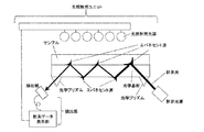
- FIG. 1 is an overall configuration diagram showing an embodiment of a photocrosslinking film manufacturing apparatus according to the present invention.
- the end face of an optical substrate is cut at an angle between 30 ° and 60 °.
- the measurement light is incident on the optical base material from the cut portion.
- FIG. 2 is an overall configuration diagram showing another embodiment of the photocrosslinking film manufacturing apparatus of the present invention.
- the end surface of the optical base material is cut at an angle of 90 °
- the optical This is an apparatus configuration in which measurement light is incident on an optical substrate using a prism.
- FIG. 3 is a diagram showing the photocrosslinking reaction of polyvinyl cinnamate.
- FIG. 4 shows the results when polyvinyl cinnamate was used before irradiation with a xenon flash lamp (total irradiation energy: 0 [J / cm 2 ]) and after irradiation (total irradiation energy: 334 [J / cm 2 ], 668 [J / cm 2 ], 735 [J / cm 2 ], 1138 [J / cm 2 ], 4551 [J / cm 2 ]) of photocrosslinkable insulator materials using FTIR (Fourier Transform Infrared Spectrometer) is there.
- FTIR Fastier Transform Infrared Spectrometer
- FIG. 5 shows specific two wavelengths 1711 [cm ⁇ 1 ] and 1721 [cm ⁇ 1 ] related to photocrosslinking measured with the total irradiation optical energy (horizontal axis) and the total reflection optical system obtained from the FTIR spectrum of FIG. 4. ] Shows the relationship with the ratio (vertical axis) of vibration absorption (absorbance) in FIG.
- FIG. 1 and 2 show an overall view of the photocrosslinking film production apparatus of the present invention.
- a total reflection optical system is used as an optical system for measurement, and a crosslinking state is analyzed during light irradiation from a light irradiation light source for photocrosslinking.
- An optical base material to be coated or printed with a material is placed in the light irradiation unit, and measurement light is incident from one end face of the optical base material under conditions where total reflection occurs at the optical base material / material interface.
- the measuring light is in the wavelength band of 1000 [cm ⁇ 1 ] to 4000 [cm ⁇ 1 ] in the infrared region, and proceeds while repeating total reflection on the upper and lower surfaces when incident from one end face of the optical substrate.
- the other end face is emitted.
- Most photocrosslinking insulating film materials have vibrational absorption representing a chemical bonding state in the infrared region, and the amount of absorption in a specific vibrational absorption band changes before and after photocrosslinking by light irradiation.
- an evanescent field is generated on the insulating film material side, Absorbed by insulating film material.
- the photocrosslinking state can be grasped by analyzing the change in the amount of absorption caused by photocrosslinking from the amount of measurement light emitted.
- the coating film can be measured in a non-contact manner without receiving interference from the light irradiation unit that irradiates the coating film surface with light. It is also suitable for measurement during light irradiation.
- [cm ⁇ 1 ] represents the number of waves contained per unit length (ie, wave number) and is often used in the spectroscopic field, but if the wavelength is constant, the wave number is equal to the reciprocal of the wavelength. Therefore, 1000 [cm ⁇ 1 ] has a wavelength of 10 ⁇ m, and 4000 [cm ⁇ 1 ] has a wavelength equal to 2.5 ⁇ m.
- the unit of wave number [cm ⁇ 1 ] may be used in the meaning of the wavelength converted into the wavelength.
- the measurement light may be incident on the optical substrate via the optical prism after an optical prism made of the same material as the optical substrate is brought into close contact with the optical substrate (see FIG. 2).
- the wavelength range is 1000 [cm ⁇ 1 ] to 4000 [cm ⁇ 1 ], and may be all light or only two wavelengths of specific wavelengths.
- the optical base material and the optical prism are preferably germanium, silicon, ZnSe, KRS-5, etc., but the real part of the complex refractive index in the band of 1000 [cm ⁇ 1 ] to 4000 [cm ⁇ 1 ] is the above-mentioned photocrosslinking insulation. It is larger than the body material and the imaginary part may be 10 ⁇ 3 or less.
- the two opposite end faces of the optical substrate are cut at 30 ° to 60 ° (see FIG. 1).
- the measurement light can enter from one end face and exit from the other end face without going through the optical prism.
- An infrared spectroscopic analyzer is used as a detector, and it is possible to detect light having a wavelength in a band of 1000 [cm ⁇ 1 ] to 4000 [cm ⁇ 1 ], and two specific wavelengths in the same band. The ratio of each vibration absorption amount (absorbance) at x1 and x2 is detected, calculated, and output.
- a film made of a photocrosslinkable material (see the sample in the figure) formed on the surface of the optical base material by a printing method or a coating method is photocrosslinked by irradiation with light in a band of 300 nm to 2 ⁇ m, thereby measuring 1000 of measurement light.
- Two specific wavelengths x1 and x2 in the band from [cm ⁇ 1 ] (wavelength 10 ⁇ m) to 4000 [cm ⁇ 1 ] (wavelength 2.5 ⁇ m) increase the amount of vibration absorption at one wavelength x2, and the other The vibration absorption amount at the wavelength x1 is limited to a decrease.
- the film thickness is preferably smaller than 2 ⁇ m.
- Light irradiation unit is low pressure mercury lamp, high pressure mercury lamp, ultra high pressure mercury lamp, xenon short arc lamp, xenon flash lamp, halogen lamp, metal halide lamp, rare gas fluorescent lamp, near ultraviolet laser, visible laser, near infrared laser, Including one or a plurality of infrared lasers, near-ultraviolet LEDs, visible LEDs, near-infrared LEDs, and a shorter wavelength side and a longer wavelength side than the wavelength band from 300 nm to 2 ⁇ m Cut out of range light. This is to prevent the measurement system from being affected by using a wavelength band different from the wavelength 1000 [cm ⁇ 1 ] to 4000 [cm ⁇ 1 ] (wavelength 10 ⁇ m to 2.5 ⁇ m) of the measurement light.
- the above-mentioned photocrosslinking type film manufacturing apparatus is used in a manufacturing line having an optical bridge type film manufacturing process during the manufacturing process, for example, a manufacturing line for electronic devices, etc. Even if there is a light absorption ratio at a specific wavelength with the amount of absorption as a baseline, in the case of manufacturing a functional film such as an insulating film with an optical bridge type material, an optical bridge type film manufacturing It can be incorporated into a production line as a manufacturing apparatus for a process, and can also be applied as an apparatus for an insulating film manufacturing process in a manufacturing line for manufacturing an electronic device using a silicon wafer or a germanium wafer.
- photocrosslinking is carried out by light irradiation using a xenon flash lamp (SINTERON 2010-L Photonic Curing R & D System, manufactured by XENON, cut wavelength of 240 nm or less) toward the coated surface.
- a xenon flash lamp SINTERON 2010-L Photonic Curing R & D System, manufactured by XENON, cut wavelength of 240 nm or less
- infrared light in a band of 1000 [cm ⁇ 1 ] to 4000 [cm ⁇ 1 ] is incident as the measurement light from the end surface of the germanium optical substrate, and the light emitted from the opposite side is spectrally analyzed, thereby polyvinyl cinnamate.
- the vibration absorption of the coating film was observed.
- FIG. 4 shows the absorbance spectrum of the emitted measurement light.
- total irradiation energy 0 J total irradiation energy
- the vibration absorption of 1711 [cm ⁇ 1 ] decreases, and the vibration absorption of 1721 [cm ⁇ 1 ] increases instead.
- vibration absorption at 1721 [cm ⁇ 1 ] is due to the vibrational energy of the adjacent carbonyl group increasing from 1711 [cm ⁇ 1 ] to 1721 [cm ⁇ 1 ] because the vinyl group is crosslinked.
- FIG. 5 is plotted against this. From FIG.
- the change in the ratio of absorbance increases greatly at the start of light irradiation, but the rate of change gradually decreases as the total irradiation energy increases, and does not change much from a point where the total irradiation energy exceeds a certain value. Therefore, it can be understood that the light irradiation in the photocrosslinking film manufacturing apparatus can be controlled by using this absorbance ratio. That is, in the example of the polyvinyl cinnamate in FIG. 5, when the absorbance ratio A x2 / A x1 exceeds about 1.08 (when the total irradiation energy exceeds about 1100 [J / cm 2 ]).
- the ratio of absorbance does not change so much, in other words, the photocrosslinking reaction does not take place so much, and at this point, the light irradiation for photocrosslinking may be terminated.
- the absorption spectrum is analyzed by infrared spectroscopic analysis in advance, and the light absorption from the light source for light irradiation is performed to perform photocrosslinking of the photocrosslinkable material.
- a specific wavelength x2 at which the vibration absorption amount is increased by the photocrosslinking of the wavelength x1 and the photocrosslinking material, that is, the absorbance is increased, and the absorbance A at the specific wavelengths x1 and x2 previously determined at the time of manufacturing the film is obtained.
- the end of light irradiation of the light source for light irradiation is controlled by the value of the ratio Ax2 / Ax1 .
- the value of the ratio A x2 / A x1 for controlling the end of light irradiation may be obtained in advance when obtaining the specific wavelengths x1 and x2, or the ratio A x2 / A x1 detected at the time of manufacture. It may be controlled to terminate the light irradiation when the change in the value of becomes small.
- the photocrosslinking film production apparatus of the invention can be used.
- the insulating film is described as an example of the functional film made of the photocrosslinking type material.
- the functional film manufacturing apparatus other than the insulating film is applicable to any film made of the photocrosslinking type material. Needless to say, you can.
Landscapes
- Physics & Mathematics (AREA)
- Health & Medical Sciences (AREA)
- Life Sciences & Earth Sciences (AREA)
- Chemical & Material Sciences (AREA)
- Analytical Chemistry (AREA)
- Biochemistry (AREA)
- General Health & Medical Sciences (AREA)
- General Physics & Mathematics (AREA)
- Immunology (AREA)
- Pathology (AREA)
- Investigating Or Analysing Materials By Optical Means (AREA)
- Manufacture Of Macromolecular Shaped Articles (AREA)
Abstract
光架橋型材料で膜を製造する際に、光照射により光架橋がどの程度進行しているかをオンラインで把握できる光架橋型膜製造装置を提供する。 光学基材の表面に形成された光架橋型材料からなる膜に、光照射して光架橋反応を行わせる光照射用光源と、前記光学基材に計測光を入射させ、前記光学基材と前記膜との界面で全反射させる計測光源と、前記光学基材から出射した計測光を分光分析する赤外分光分析機を備え、赤外分光分析機は、予め、前記光学基材から出射した計測光の吸光度スペクトルを分析して光架橋型材料の光架橋反応の進展にともない吸光度が減少する特定波長x1、および吸光度が増加する特定波長x2を求めておき、予め求めていた特定波長x1、x2における吸光度Ax1、Ax2の比Ax2/Ax1を演算し、当該比の値により前記光照射用光源を制御することを特徴とする。
Description
本発明は、光架橋型膜製造装置に関し、特に、光照射条件をオンライン制御可能にした光架橋型膜製造装置に関する。
従来、絶縁膜などの機能性膜の材料のひとつとして光架橋型材料が知られており、例えばエレクトロニクスデバイスでは、印刷法や塗布法を利用した素子形成時に必要となる絶縁膜の材料の有力な候補のひとつである(非特許文献1~3、特許文献1~2参照)。
Polymer International 43, 1997, 310-316.
Journal of Materials Chemistry 2011, 21, 15637-15642.
Chemistry of Materials 2004, 16, 5141-5148.
しかしながら、光架橋型材料で絶縁膜などの機能性膜を製造する際には、光照射により光架橋がどの程度進行しているかをオンラインで把握することが困難であった。機能性膜として絶縁膜の製造を一例にとれば、基材表面に印刷あるいは塗布された絶縁体前駆体膜表面への光照射時に光架橋がどの程度進行しているかを把握し光照射条件を最適化するためには、膨大なデータ取得が必要となり、最適化条件の探索の効率化が課題となっている。
したがって、本発明の解決しようとする課題は、光架橋型材料で機能性膜を製造する際に、光照射により光架橋がどの程度進行しているかをオンラインで把握し光照射条件を最適化する光架橋型膜製造装置を提供することにある。
したがって、本発明の解決しようとする課題は、光架橋型材料で機能性膜を製造する際に、光照射により光架橋がどの程度進行しているかをオンラインで把握し光照射条件を最適化する光架橋型膜製造装置を提供することにある。
上記課題を解決するために、本発明は、光学基材の表面に形成された光架橋型材料からなる膜に、光照射して光架橋反応を行わせる光照射用光源と、前記光学基材に計測光を入射させ、前記光学基材と前記膜との界面で全反射させる計測光源と、前記光学基材から出射した計測光を分光分析する赤外分光分析機を備えた光架橋型膜製造装置であって、
前記赤外分光分析機は、
予め、前記光学基材から出射した計測光の吸光度スペクトルを分析して前記光架橋型材料の光架橋反応の進展にともない吸光度が減少する特定波長x1、および前記光架橋型材料の光架橋反応の進展にともない吸光度が増加する特定波長x2を求めておき、
前記予め求めていた特定波長x1、x2における吸光度Ax1、Ax2の比Ax2/Ax1を演算し、当該比の値により前記光照射用光源を制御することを特徴とする。
また、本発明は、上記光架橋型膜製造装置において、前記計測光源からの計測光は1000[cm-1]から4000[cm-1]の帯域中の波長の光を用いることを特徴とする。
また、本発明は、上記光架橋型膜製造装置において、前記光照射用光源からの光照射は波長300nmから2μmまでの帯域の光を照射し、前記光架橋型材料は波長300nmから2μmまでの帯域の光で光架橋するものであることを特徴とする。
また、本発明は、上記光架橋型膜製造装置において、前記光学基材は、1000[cm-1]から4000[cm-1]の帯域で複素屈折率の実数部が前記光架橋型材料よりも大きく、虚数部が10-3以下であることを特徴とする。
また、本発明は、上記光架橋型膜製造装置において、前記光照射用光源の制御は、前記比の値が一定の値に達しない場合は、一定の値に達するまで前記光照射を行い続けることを特徴とする。
また、本発明は、上記光架橋型膜製造装置において、前記計測光の光学基材への入射および出射は、光学基材端面のカット面または光学基材に密着させたプリズムを介して行うことを特徴とする。
また、本発明は、上記光架橋型膜製造装置において、前記光架橋型膜は絶縁膜であることを特徴とする。
また、本発明は、光学基材の表面に形成された光架橋型材料からなる膜に、光照射して光架橋反応を行わせ、前記光学基材と前記膜との界面で全反射するように、計測光を光学基材に入射し、光学基材から出射した計測光を赤外分光分析機で分光分析する光架橋型膜製造方法であって、
予め、計測光の吸光度スペクトルを分析して前記光架橋型材料の光架橋反応の進展にともない吸光度が減少する特定波長x1、および前記光架橋型材料の光架橋反応の進展にともない吸光度が増加する特定波長x2を求めておき、前記予め求めていた特定波長x1、x2における吸光度Ax1、Ax2の比Ax2/Ax1を用いて前記光照射を制御することを特徴とする。
前記赤外分光分析機は、
予め、前記光学基材から出射した計測光の吸光度スペクトルを分析して前記光架橋型材料の光架橋反応の進展にともない吸光度が減少する特定波長x1、および前記光架橋型材料の光架橋反応の進展にともない吸光度が増加する特定波長x2を求めておき、
前記予め求めていた特定波長x1、x2における吸光度Ax1、Ax2の比Ax2/Ax1を演算し、当該比の値により前記光照射用光源を制御することを特徴とする。
また、本発明は、上記光架橋型膜製造装置において、前記計測光源からの計測光は1000[cm-1]から4000[cm-1]の帯域中の波長の光を用いることを特徴とする。
また、本発明は、上記光架橋型膜製造装置において、前記光照射用光源からの光照射は波長300nmから2μmまでの帯域の光を照射し、前記光架橋型材料は波長300nmから2μmまでの帯域の光で光架橋するものであることを特徴とする。
また、本発明は、上記光架橋型膜製造装置において、前記光学基材は、1000[cm-1]から4000[cm-1]の帯域で複素屈折率の実数部が前記光架橋型材料よりも大きく、虚数部が10-3以下であることを特徴とする。
また、本発明は、上記光架橋型膜製造装置において、前記光照射用光源の制御は、前記比の値が一定の値に達しない場合は、一定の値に達するまで前記光照射を行い続けることを特徴とする。
また、本発明は、上記光架橋型膜製造装置において、前記計測光の光学基材への入射および出射は、光学基材端面のカット面または光学基材に密着させたプリズムを介して行うことを特徴とする。
また、本発明は、上記光架橋型膜製造装置において、前記光架橋型膜は絶縁膜であることを特徴とする。
また、本発明は、光学基材の表面に形成された光架橋型材料からなる膜に、光照射して光架橋反応を行わせ、前記光学基材と前記膜との界面で全反射するように、計測光を光学基材に入射し、光学基材から出射した計測光を赤外分光分析機で分光分析する光架橋型膜製造方法であって、
予め、計測光の吸光度スペクトルを分析して前記光架橋型材料の光架橋反応の進展にともない吸光度が減少する特定波長x1、および前記光架橋型材料の光架橋反応の進展にともない吸光度が増加する特定波長x2を求めておき、前記予め求めていた特定波長x1、x2における吸光度Ax1、Ax2の比Ax2/Ax1を用いて前記光照射を制御することを特徴とする。
本発明では、計測系として、全反射光学系を利用することにより、光架橋用照射光源の干渉を受けることなく、基材の裏面側に計測系を組むことが可能である。
また、光架橋用照射光源と計測系で用いられる光源は、波長帯域が異なるため、計測時に光架橋用照射光からのノイズはフィルタの導入などでカットしやすく、光架橋のための光照射の最中に連続的な計測が可能である。
計測光の強度は、光架橋反応を促進させないような大きさが望ましいところ、本発明では、例えば、1[mW]以下の強度でも検出器の感度を上げれば計測は十分可能である。
また、光架橋用照射光源と計測系で用いられる光源は、波長帯域が異なるため、計測時に光架橋用照射光からのノイズはフィルタの導入などでカットしやすく、光架橋のための光照射の最中に連続的な計測が可能である。
計測光の強度は、光架橋反応を促進させないような大きさが望ましいところ、本発明では、例えば、1[mW]以下の強度でも検出器の感度を上げれば計測は十分可能である。
図1および図2に本発明の光架橋型膜製造装置の全体図を示す。本発明では、計測のための光学系に全反射光学系を利用し、光架橋のための光照射用光源から光照射を行っている最中に架橋状態を解析する。光照射ユニット内に、材料塗布あるいは印刷される光学基材を置き、光学基材と材料界面で全反射が起こるような条件で計測光を光学基材の一方の端面から入射する。計測光は、赤外領域の1000[cm-1]から4000[cm-1]の波長帯域にあり、光学基材の一方の端面から入射されると上面と下面で全反射を繰り返しながら進行し、もう一方の端面がら出射される。光架橋型の絶縁膜材料の多くは、赤外領域に化学結合状態を表す振動吸収があり、光照射による光架橋前後で特定の振動吸収帯における吸収量が変化する。光学基材に入射された計測光は、塗布あるいは印刷された光架橋型絶縁膜材料が存在する部分と光学基材との界面で全反射する際に、絶縁膜材料側にエバネセント場を生じ、絶縁膜材料に吸収される。このうち、光架橋に起因する吸収量変化を出射してくる計測光の光量から解析することによって、光架橋状態を把握することが出来る。
計測のための光学系は、光学基材の裏面側に組むことができるため、塗布膜表面へ光照射を行う光照射ユニットの干渉を受けることなく、塗布膜には非接触で計測できるため、光照射中の計測にも適している。
ここで、[cm-1]は単位長さ当たりに含まれる波の数(すなわち波数)を表すもので分光分野においてよく用いられているが、波長が一定であれば波数は波長の逆数に等しくなるので、1000[cm-1]は波長10μm、4000[cm-1]は波長2.5μmに等しくなる。なお、本発明では波長が一定であるものとして扱っても差し支えないから、以下の説明では波数の単位[cm-1]を波長に換算した波長の意味で用いている場合もある。
計測のための光学系は、光学基材の裏面側に組むことができるため、塗布膜表面へ光照射を行う光照射ユニットの干渉を受けることなく、塗布膜には非接触で計測できるため、光照射中の計測にも適している。
ここで、[cm-1]は単位長さ当たりに含まれる波の数(すなわち波数)を表すもので分光分野においてよく用いられているが、波長が一定であれば波数は波長の逆数に等しくなるので、1000[cm-1]は波長10μm、4000[cm-1]は波長2.5μmに等しくなる。なお、本発明では波長が一定であるものとして扱っても差し支えないから、以下の説明では波数の単位[cm-1]を波長に換算した波長の意味で用いている場合もある。
計測光は、光学基材と同素材から成る光学プリズムを光学基材に密着させ、光学プリズムを介して光学基材に入射してもよい(図2参照)。波長範囲は、1000[cm-1]から4000[cm-1]であり、全光あるいは特定波長の2波長だけでもよい。
光学基材および光学プリズムは、ゲルマニウム、シリコン、ZnSe、KRS―5などが望ましいが、1000[cm-1]から4000[cm-1]の帯域で複素屈折率の実数部が前記光架橋型絶縁体材料よりも大きく、虚数部が10-3以下であればよい。光学基材の向かい合う2つの端面は30°~60°にカットされていることが望ましい(図1参照)。この場合、光学プリズムを介さずに計測光を一方の端面から入射しもう一方の端面から出射させることができる。
検出器には赤外分光分析機を用い、1000[cm-1]から4000[cm-1]の帯域中の波長の光を検出することが可能であり、且つ同帯域中の2つの特定波長x1、x2におけるそれぞれの振動吸収量(吸光度)の比を検出および計算し出力するものである。
印刷法や塗布法により光学基材表面に形成された光架橋型材料からなる膜(図中のサンプル参照)は、300nmから2μmまでの帯域の光照射によって光架橋し、これによって計測光の1000[cm-1](波長10μm)から4000[cm-1](波長2.5μm)における帯域中の2つの特定波長x1、x2は、一方の波長x2における振動吸収量が増加し、もう一方の波長x1における振動吸収量が減少するものに限定される。また、膜厚は概ね2μmより小さいことが望ましい。
光照射ユニットは、低圧水銀ランプ、高圧水銀ランプ、超高圧水銀ランプ、キセノンショートアークランプ、キセノンフラッシュランプ、ハロゲンランプ、メタルハライドランプ、希ガス蛍光ランプ、近紫外レーザー、可視レーザー、近赤外レーザー、赤外レーザー、近紫外LED、可視LED、近赤外LEDのいずれか、あるいは複数を含み、300nmから2μmの波長帯域よりも短波長側および長波長側を含む場合は、フィルタにより300nmから2μmの範囲外の光をカットする。これは、計測光の波長1000[cm-1]~4000[cm-1](波長10μm~2.5μm)と異なる波長帯域を用いることで計測系に影響を及ぼさないようにするためである。
光学基材および光学プリズムは、ゲルマニウム、シリコン、ZnSe、KRS―5などが望ましいが、1000[cm-1]から4000[cm-1]の帯域で複素屈折率の実数部が前記光架橋型絶縁体材料よりも大きく、虚数部が10-3以下であればよい。光学基材の向かい合う2つの端面は30°~60°にカットされていることが望ましい(図1参照)。この場合、光学プリズムを介さずに計測光を一方の端面から入射しもう一方の端面から出射させることができる。
検出器には赤外分光分析機を用い、1000[cm-1]から4000[cm-1]の帯域中の波長の光を検出することが可能であり、且つ同帯域中の2つの特定波長x1、x2におけるそれぞれの振動吸収量(吸光度)の比を検出および計算し出力するものである。
印刷法や塗布法により光学基材表面に形成された光架橋型材料からなる膜(図中のサンプル参照)は、300nmから2μmまでの帯域の光照射によって光架橋し、これによって計測光の1000[cm-1](波長10μm)から4000[cm-1](波長2.5μm)における帯域中の2つの特定波長x1、x2は、一方の波長x2における振動吸収量が増加し、もう一方の波長x1における振動吸収量が減少するものに限定される。また、膜厚は概ね2μmより小さいことが望ましい。
光照射ユニットは、低圧水銀ランプ、高圧水銀ランプ、超高圧水銀ランプ、キセノンショートアークランプ、キセノンフラッシュランプ、ハロゲンランプ、メタルハライドランプ、希ガス蛍光ランプ、近紫外レーザー、可視レーザー、近赤外レーザー、赤外レーザー、近紫外LED、可視LED、近赤外LEDのいずれか、あるいは複数を含み、300nmから2μmの波長帯域よりも短波長側および長波長側を含む場合は、フィルタにより300nmから2μmの範囲外の光をカットする。これは、計測光の波長1000[cm-1]~4000[cm-1](波長10μm~2.5μm)と異なる波長帯域を用いることで計測系に影響を及ぼさないようにするためである。
上記の光架橋型膜製造装置は、製造工程中に光橋架型膜製造工程を有する製造ライン、例えば、エレクトロニクスデバイス等の製造ラインにおいて、基板の材質が特定波長に吸収を持たない、あるいは、吸収があるとしてもこの吸収量をベースラインとして、特定波長における吸光度の比をとることができれば、光橋架型材料で絶縁膜等の機能性膜を製造するような場合には、光橋架型膜製造工程の製造装置として製造ライン中に組み込むことができ、シリコンウエハーやゲルマニウムウエハーを用いてエレクトロニクスデバイスを製造する製造ライン中の、絶縁膜製造工程の装置としても適用できる。
光架橋型材料としてポリビニルシンナメートを用いて絶縁膜を製造する場合を以下に説明する。ポリビニルシンナメートの光架橋反応は、図3に示すとおりである。
2[wt.%]のポリビニルシンナメートのクロロホルム溶液を60°に端面がカットされたゲルマニウム光学基材表面に膜厚が500[nm]になるよう塗布し、ホットプレート上で100℃、5分間の熱処理によりクロロホルムを蒸発させた後、塗布面に向けてキセノンフラッシュランプ(SINTERON 2010-L Photonic Curing R&D System、XENON社製、240nm以下の波長をカット)を用いて光照射による光架橋を行う。また、計測光として1000[cm-1]から4000[cm-1]の帯域の赤外光をゲルマニウム光学基材端面から入射し、反対側から出射した光を分光分析することによって、ポリビニルシンナメート塗布膜の振動吸収を観察した。
出射した計測光の吸光度スペクトルを図4に示す。光照射前(照射エネルギー総量0J)には、カルボニル基由来の振動吸収が1711[cm-1]に現れている。光照射を行うと、照射総エネルギー(照射エネルギー総量334[J/cm2]、334[J/cm2]、668[J/cm2]、735[J/cm2]、1138[J/cm2]、4551[J/cm2])が増えるにつれて1711[cm-1]の振動吸収が減少し、代わりに1721[cm-1]の振動吸収が増加している。これは、1721[cm-1]における振動吸収は、ビニル基が架橋したために隣のカルボニル基の振動エネルギーが1711[cm-1]から1721[cm-1]に増大したためである。
この2つの波長x1(=1711[cm-1])、x2(=1721[cm-1])における吸光度Ax1、Ax2の比Ax2/Ax1を照射総エネルギー[J/cm2]に対してプロットしたのが図5である。図5から吸光度の比の変化は、光照射開始時には大きく増大するが照射総エネルギーの増加につれて次第に変化率は小さくなり、照射総エネルギーがある値を超えたところからあまり変化しなくなる。したがって、この吸光度の比を利用すれば、光架橋型膜製造装置における光照射の制御が行えることがわかる。すなわち、図5のポリビニルシンナメートの例でいえば、吸光度の比Ax2/Ax1が略1.08を越えるころ(照射総エネルギーでいえば略1100[J/cm2]を越えたころ)から吸光度の比はあまり変化しなくなり、言い換えれば光架橋反応があまり行われなくなり、この時点で光架橋のための光照射を終了させて良いことがわかる。
つまり、予め、赤外分光分析によって吸光度スペクトルを解析して、光照射用光源から光照射を行って光架橋型材料の光架橋が行われることにより振動吸収量が減少するすなわち吸光度が減少する特定波長x1、光架橋型材料の光架橋が行われることにより振動吸収量が増加するすなわち吸光度が増加する特定波長x2を求めておき、膜製造時には予め求めていた当該特定波長x1、x2における吸光度Ax1、Ax2を検出しその比Ax2/Ax1の値により光照射用光源の光照射の終了を制御する。なお、光照射の終了を制御する比Ax2/Ax1の値は、予め特定波長x1、x2を求める際に同時に求めておいてもよいし、製造時に検出している比Ax2/Ax1の値の変化が小さくなったら光照射の終了を行うように制御しても良い。
2[wt.%]のポリビニルシンナメートのクロロホルム溶液を60°に端面がカットされたゲルマニウム光学基材表面に膜厚が500[nm]になるよう塗布し、ホットプレート上で100℃、5分間の熱処理によりクロロホルムを蒸発させた後、塗布面に向けてキセノンフラッシュランプ(SINTERON 2010-L Photonic Curing R&D System、XENON社製、240nm以下の波長をカット)を用いて光照射による光架橋を行う。また、計測光として1000[cm-1]から4000[cm-1]の帯域の赤外光をゲルマニウム光学基材端面から入射し、反対側から出射した光を分光分析することによって、ポリビニルシンナメート塗布膜の振動吸収を観察した。
出射した計測光の吸光度スペクトルを図4に示す。光照射前(照射エネルギー総量0J)には、カルボニル基由来の振動吸収が1711[cm-1]に現れている。光照射を行うと、照射総エネルギー(照射エネルギー総量334[J/cm2]、334[J/cm2]、668[J/cm2]、735[J/cm2]、1138[J/cm2]、4551[J/cm2])が増えるにつれて1711[cm-1]の振動吸収が減少し、代わりに1721[cm-1]の振動吸収が増加している。これは、1721[cm-1]における振動吸収は、ビニル基が架橋したために隣のカルボニル基の振動エネルギーが1711[cm-1]から1721[cm-1]に増大したためである。
この2つの波長x1(=1711[cm-1])、x2(=1721[cm-1])における吸光度Ax1、Ax2の比Ax2/Ax1を照射総エネルギー[J/cm2]に対してプロットしたのが図5である。図5から吸光度の比の変化は、光照射開始時には大きく増大するが照射総エネルギーの増加につれて次第に変化率は小さくなり、照射総エネルギーがある値を超えたところからあまり変化しなくなる。したがって、この吸光度の比を利用すれば、光架橋型膜製造装置における光照射の制御が行えることがわかる。すなわち、図5のポリビニルシンナメートの例でいえば、吸光度の比Ax2/Ax1が略1.08を越えるころ(照射総エネルギーでいえば略1100[J/cm2]を越えたころ)から吸光度の比はあまり変化しなくなり、言い換えれば光架橋反応があまり行われなくなり、この時点で光架橋のための光照射を終了させて良いことがわかる。
つまり、予め、赤外分光分析によって吸光度スペクトルを解析して、光照射用光源から光照射を行って光架橋型材料の光架橋が行われることにより振動吸収量が減少するすなわち吸光度が減少する特定波長x1、光架橋型材料の光架橋が行われることにより振動吸収量が増加するすなわち吸光度が増加する特定波長x2を求めておき、膜製造時には予め求めていた当該特定波長x1、x2における吸光度Ax1、Ax2を検出しその比Ax2/Ax1の値により光照射用光源の光照射の終了を制御する。なお、光照射の終了を制御する比Ax2/Ax1の値は、予め特定波長x1、x2を求める際に同時に求めておいてもよいし、製造時に検出している比Ax2/Ax1の値の変化が小さくなったら光照射の終了を行うように制御しても良い。
印刷エレクトロニクスは近年発展著しい分野であるが、印刷法や塗布法を利用したアクティブ素子製造時に必要となる絶縁膜材料には光架橋型の材料も多く存在するので、印刷エレクトロニクスデバイスの製造ラインに本発明の光架橋型膜製造装置を利用することができる。
また、上記説明では、光架橋型の材料による機能性膜の一例として絶縁膜で説明したが、絶縁膜以外の機能性膜の製造装置であっても、光架橋型材料による膜であれば適用できることは言うまでもない。
また、上記説明では、光架橋型の材料による機能性膜の一例として絶縁膜で説明したが、絶縁膜以外の機能性膜の製造装置であっても、光架橋型材料による膜であれば適用できることは言うまでもない。
Claims (8)
- 光学基材の表面に形成された光架橋型材料からなる膜に、光照射して光架橋反応を行わせる光照射用光源と、
前記光学基材に計測光を入射させ、前記光学基材と前記膜との界面で全反射させる計測光源と、
前記光学基材から出射した計測光を分光分析する赤外分光分析機を備えた光架橋型膜製造装置であって、
前記赤外分光分析機は、
予め、前記光学基材から出射した計測光の吸光度スペクトルを分析して前記光架橋型材料の光架橋反応の進展にともない吸光度が減少する特定波長x1、および前記光架橋型材料の光架橋反応の進展にともない吸光度が増加する特定波長x2を求めておき、
前記予め求めていた特定波長x1、x2における吸光度Ax1、Ax2の比Ax2/Ax1を演算し、当該比の値により前記光照射用光源を制御することを特徴とする光架橋型膜製造装置。 - 前記計測光源からの計測光は1000[cm-1]から4000[cm-1]の帯域中の波長の光を用いることを特徴とする請求項1記載の光架橋型膜製造装置。
- 前記光照射用光源からの光照射は波長300nmから2μmまでの帯域の光を照射し、
前記光架橋型材料は波長300nmから2μmまでの帯域の光で光架橋するものであることを特徴とする請求項1又は2記載の光架橋型膜製造装置。 - 前記光学基材は、1000[cm-1]から4000[cm-1]の帯域で複素屈折率の実数部が前記光架橋型材料よりも大きく、虚数部が10-3以下であることを特徴とする請求項1~3のいずれかに記載の光架橋型膜製造装置。
- 前記光照射用光源の制御は、前記比の値が一定の値に達しない場合は、一定の値に達するまで前記光照射を行い続けることを特徴とする請求項1~4のいずれかに記載の光架橋型膜製造装置。
- 前記計測光の光学基材への入射および出射は、光学基材端面のカット面または光学基材に密着させたプリズムを介して行うことを特徴とする請求項1~5のいずれかに記載の光架橋型膜製造装置。
- 前記光架橋型膜は絶縁膜であることを特徴とする請求項1~6のいずれかに記載の光架橋型膜製造装置。
- 光学基材の表面に形成された光架橋型材料からなる膜に、光照射して光架橋反応を行わせ、
前記光学基材と前記膜との界面で全反射するように、計測光を光学基材に入射し、光学基材から出射した計測光を赤外分光分析機で分光分析する光架橋型膜製造方法であって、
予め、計測光の吸光度スペクトルを分析して前記光架橋型材料の光架橋反応の進展にともない吸光度が減少する特定波長x1、および前記光架橋型材料の光架橋反応の進展にともない吸光度が増加する特定波長x2を求めておき、
前記予め求めていた特定波長x1、x2における吸光度Ax1、Ax2の比Ax2/Ax1を用いて前記光照射を制御することを特徴とする光架橋型膜製造方法。
Priority Applications (1)
| Application Number | Priority Date | Filing Date | Title |
|---|---|---|---|
| JP2016538274A JPWO2016017464A1 (ja) | 2014-07-30 | 2015-07-17 | 光架橋型膜製造装置 |
Applications Claiming Priority (2)
| Application Number | Priority Date | Filing Date | Title |
|---|---|---|---|
| JP2014-154417 | 2014-07-30 | ||
| JP2014154417 | 2014-07-30 |
Publications (1)
| Publication Number | Publication Date |
|---|---|
| WO2016017464A1 true WO2016017464A1 (ja) | 2016-02-04 |
Family
ID=55217367
Family Applications (1)
| Application Number | Title | Priority Date | Filing Date |
|---|---|---|---|
| PCT/JP2015/070605 Ceased WO2016017464A1 (ja) | 2014-07-30 | 2015-07-17 | 光架橋型膜製造装置 |
Country Status (2)
| Country | Link |
|---|---|
| JP (1) | JPWO2016017464A1 (ja) |
| WO (1) | WO2016017464A1 (ja) |
Citations (2)
| Publication number | Priority date | Publication date | Assignee | Title |
|---|---|---|---|---|
| JPS6365343A (ja) * | 1986-09-08 | 1988-03-23 | Hitachi Ltd | 感光性材料の光学特性測定装置 |
| JP2013238591A (ja) * | 2012-05-15 | 2013-11-28 | Palo Alto Research Center Inc | 感光性樹脂膜の重合監視のための低コストの測定システム |
Family Cites Families (4)
| Publication number | Priority date | Publication date | Assignee | Title |
|---|---|---|---|---|
| JP3227866B2 (ja) * | 1993-02-17 | 2001-11-12 | 住友電気工業株式会社 | 硬化反応の測定方法及び装置 |
| JP3839703B2 (ja) * | 2001-11-05 | 2006-11-01 | 浜松ホトニクス株式会社 | 樹脂硬化度測定装置 |
| JP5481689B2 (ja) * | 2008-08-26 | 2014-04-23 | アクアス株式会社 | イオン測定用オプトード及びそれを用いたイオン濃度の測定方法 |
| JP5576696B2 (ja) * | 2010-04-14 | 2014-08-20 | 日本分光株式会社 | 紫外線硬化樹脂の物性測定装置 |
-
2015
- 2015-07-17 JP JP2016538274A patent/JPWO2016017464A1/ja active Pending
- 2015-07-17 WO PCT/JP2015/070605 patent/WO2016017464A1/ja not_active Ceased
Patent Citations (2)
| Publication number | Priority date | Publication date | Assignee | Title |
|---|---|---|---|---|
| JPS6365343A (ja) * | 1986-09-08 | 1988-03-23 | Hitachi Ltd | 感光性材料の光学特性測定装置 |
| JP2013238591A (ja) * | 2012-05-15 | 2013-11-28 | Palo Alto Research Center Inc | 感光性樹脂膜の重合監視のための低コストの測定システム |
Also Published As
| Publication number | Publication date |
|---|---|
| JPWO2016017464A1 (ja) | 2017-04-27 |
Similar Documents
| Publication | Publication Date | Title |
|---|---|---|
| Perney et al. | Tuning localized plasmon cavities for optimized surface-enhanced Raman scattering | |
| EP2764403B1 (en) | Hydrogen passivation of nonlinear optical crystals | |
| CN110546749A (zh) | 用于蚀刻处理监测的高级光学传感器、系统和方法 | |
| US20200043710A1 (en) | Normal-incident in-situ process monitor sensor | |
| US8708557B2 (en) | Apparatus for measuring thermal diffusivity | |
| US20200326475A1 (en) | Microsphere Based Patterning of Metal Optic/Plasmonic Sensors Including Fiber Based Sensors | |
| JP6072613B2 (ja) | プラズマ処理方法 | |
| WO2015171149A1 (en) | Optical transmission/reflection mode in-situ deposition rate control for ice fabrication | |
| CN104655278B (zh) | 一种波长定标仪 | |
| CN106053355B (zh) | 光刻胶的参数检测方法及装置 | |
| CN111413314A (zh) | 一种基于贝塞尔光的便携式拉曼光谱仪 | |
| CN107631993A (zh) | 一种基于水汽残差谱分析的红外光谱识别方法 | |
| CN110426371A (zh) | 一种检测sf6电气设备中的hf气体的系统 | |
| CN116481444A (zh) | 一种基于透射光谱的塑料薄膜厚度测量系统及测量方法 | |
| CN1554107A (zh) | 用于确定实时蚀刻速率的浅角干涉工艺及装置 | |
| US9366601B1 (en) | Wafer fabrication monitoring/control system and method | |
| JPWO2016017464A1 (ja) | 光架橋型膜製造装置 | |
| KR20030000274A (ko) | 반도체 제조공정에서 실시간 플라즈마 측정과 박막분석을위한 다채널 분광분석기 | |
| CN107250768A (zh) | 用于uv硬化的工艺监控 | |
| US20210142991A1 (en) | Apparatus with optical cavity for determining process rate | |
| US20160265910A1 (en) | In-situ analysis of ice using surface acoustic wave spectroscopy | |
| CN105181605B (zh) | 一种基于布拉格反射效应的光谱仪 | |
| Kim et al. | In-situ non-contact monitoring of photoresist thickness and degree of cure using terahertz time-domain spectroscopy | |
| Airoudj et al. | Improvement of the optical transmission of polymer planar waveguides by plasma treatment | |
| CN107328737A (zh) | 一种测量气体吸收光谱的装置及方法 |
Legal Events
| Date | Code | Title | Description |
|---|---|---|---|
| 121 | Ep: the epo has been informed by wipo that ep was designated in this application |
Ref document number: 15826688 Country of ref document: EP Kind code of ref document: A1 |
|
| ENP | Entry into the national phase |
Ref document number: 2016538274 Country of ref document: JP Kind code of ref document: A |
|
| NENP | Non-entry into the national phase |
Ref country code: DE |
|
| 122 | Ep: pct application non-entry in european phase |
Ref document number: 15826688 Country of ref document: EP Kind code of ref document: A1 |