WO2016017303A1 - エッチング特性推定方法、プログラム、情報処理装置、加工装置、設計方法、および、製造方法 - Google Patents
エッチング特性推定方法、プログラム、情報処理装置、加工装置、設計方法、および、製造方法 Download PDFInfo
- Publication number
- WO2016017303A1 WO2016017303A1 PCT/JP2015/067141 JP2015067141W WO2016017303A1 WO 2016017303 A1 WO2016017303 A1 WO 2016017303A1 JP 2015067141 W JP2015067141 W JP 2015067141W WO 2016017303 A1 WO2016017303 A1 WO 2016017303A1
- Authority
- WO
- WIPO (PCT)
- Prior art keywords
- protective film
- film layer
- etching
- workpiece
- fluxes
- Prior art date
- Legal status (The legal status is an assumption and is not a legal conclusion. Google has not performed a legal analysis and makes no representation as to the accuracy of the status listed.)
- Ceased
Links
Images


Classifications
-
- H—ELECTRICITY
- H01—ELECTRIC ELEMENTS
- H01L—SEMICONDUCTOR DEVICES NOT COVERED BY CLASS H10
- H01L21/00—Processes or apparatus adapted for the manufacture or treatment of semiconductor or solid state devices or of parts thereof
- H01L21/67—Apparatus specially adapted for handling semiconductor or electric solid state devices during manufacture or treatment thereof; Apparatus specially adapted for handling wafers during manufacture or treatment of semiconductor or electric solid state devices or components ; Apparatus not specifically provided for elsewhere
- H01L21/67005—Apparatus not specifically provided for elsewhere
- H01L21/67011—Apparatus for manufacture or treatment
- H01L21/67017—Apparatus for fluid treatment
- H01L21/67063—Apparatus for fluid treatment for etching
- H01L21/67069—Apparatus for fluid treatment for etching for drying etching
-
- G—PHYSICS
- G03—PHOTOGRAPHY; CINEMATOGRAPHY; ANALOGOUS TECHNIQUES USING WAVES OTHER THAN OPTICAL WAVES; ELECTROGRAPHY; HOLOGRAPHY
- G03F—PHOTOMECHANICAL PRODUCTION OF TEXTURED OR PATTERNED SURFACES, e.g. FOR PRINTING, FOR PROCESSING OF SEMICONDUCTOR DEVICES; MATERIALS THEREFOR; ORIGINALS THEREFOR; APPARATUS SPECIALLY ADAPTED THEREFOR
- G03F1/00—Originals for photomechanical production of textured or patterned surfaces, e.g., masks, photo-masks, reticles; Mask blanks or pellicles therefor; Containers specially adapted therefor; Preparation thereof
- G03F1/36—Masks having proximity correction features; Preparation thereof, e.g. optical proximity correction [OPC] design processes
-
- G—PHYSICS
- G05—CONTROLLING; REGULATING
- G05B—CONTROL OR REGULATING SYSTEMS IN GENERAL; FUNCTIONAL ELEMENTS OF SUCH SYSTEMS; MONITORING OR TESTING ARRANGEMENTS FOR SUCH SYSTEMS OR ELEMENTS
- G05B13/00—Adaptive control systems, i.e. systems automatically adjusting themselves to have a performance which is optimum according to some preassigned criterion
- G05B13/02—Adaptive control systems, i.e. systems automatically adjusting themselves to have a performance which is optimum according to some preassigned criterion electric
- G05B13/04—Adaptive control systems, i.e. systems automatically adjusting themselves to have a performance which is optimum according to some preassigned criterion electric involving the use of models or simulators
- G05B13/041—Adaptive control systems, i.e. systems automatically adjusting themselves to have a performance which is optimum according to some preassigned criterion electric involving the use of models or simulators in which a variable is automatically adjusted to optimise the performance
-
- G—PHYSICS
- G06—COMPUTING OR CALCULATING; COUNTING
- G06F—ELECTRIC DIGITAL DATA PROCESSING
- G06F30/00—Computer-aided design [CAD]
- G06F30/30—Circuit design
- G06F30/36—Circuit design at the analogue level
- G06F30/367—Design verification, e.g. using simulation, simulation program with integrated circuit emphasis [SPICE], direct methods or relaxation methods
-
- G—PHYSICS
- G06—COMPUTING OR CALCULATING; COUNTING
- G06F—ELECTRIC DIGITAL DATA PROCESSING
- G06F30/00—Computer-aided design [CAD]
- G06F30/30—Circuit design
- G06F30/39—Circuit design at the physical level
- G06F30/398—Design verification or optimisation, e.g. using design rule check [DRC], layout versus schematics [LVS] or finite element methods [FEM]
-
- H—ELECTRICITY
- H01—ELECTRIC ELEMENTS
- H01L—SEMICONDUCTOR DEVICES NOT COVERED BY CLASS H10
- H01L21/00—Processes or apparatus adapted for the manufacture or treatment of semiconductor or solid state devices or of parts thereof
- H01L21/02—Manufacture or treatment of semiconductor devices or of parts thereof
- H01L21/04—Manufacture or treatment of semiconductor devices or of parts thereof the devices having potential barriers, e.g. a PN junction, depletion layer or carrier concentration layer
- H01L21/18—Manufacture or treatment of semiconductor devices or of parts thereof the devices having potential barriers, e.g. a PN junction, depletion layer or carrier concentration layer the devices having semiconductor bodies comprising elements of Group IV of the Periodic Table or AIIIBV compounds with or without impurities, e.g. doping materials
- H01L21/30—Treatment of semiconductor bodies using processes or apparatus not provided for in groups H01L21/20 - H01L21/26
- H01L21/31—Treatment of semiconductor bodies using processes or apparatus not provided for in groups H01L21/20 - H01L21/26 to form insulating layers thereon, e.g. for masking or by using photolithographic techniques; After treatment of these layers; Selection of materials for these layers
- H01L21/3105—After-treatment
- H01L21/311—Etching the insulating layers by chemical or physical means
- H01L21/31105—Etching inorganic layers
- H01L21/31111—Etching inorganic layers by chemical means
- H01L21/31116—Etching inorganic layers by chemical means by dry-etching
Definitions
- the present technology relates to an etching characteristic estimation method, a program for causing a computer to execute the method, an information processing device, a processing device, a design method, and a manufacturing method.
- the present invention relates to an etching characteristic estimation method for estimating etching characteristics of dry etching, a program for causing a computer to execute the method, an information processing apparatus, a processing apparatus, a design method, and a manufacturing method.
- the present technology has been developed in view of such a situation, and an object thereof is to obtain etching characteristics when a workpiece contains a nitrogen compound and hydrogen is contained in an etching gas such as a CHxFy-based gas. .
- a first aspect of the present technology is that an information processing apparatus is used in a surface reaction model in which a processing surface of a workpiece includes a protective film layer and a reaction layer.
- An etching characteristic estimation method including a protective film layer calculation procedure for calculating the thickness of the protective film layer by switching the removal term according to a comparison result of flux, and a program for executing the method. This brings about the effect that the etching characteristics can be predicted by reflecting that the removal term is switched according to the comparison result of the plurality of fluxes.
- the plurality of fluxes may include an incident flux incident on the processing surface and an outflux released by etching the workpiece. Thereby, the removal term is switched according to the comparison result of the incident flux and the outflux.
- the plurality of fluxes may include at least nitrogen and hydrogen fluxes.
- the removal term is switched according to the comparison result of the fluxes of nitrogen and hydrogen.
- the information processing apparatus may switch the removal term to any one of at least three different terms according to the comparison result in the protective film layer calculation procedure. This brings about the effect that the removal term is switched to any one of at least three different terms.
- the information processing apparatus may switch the removal term in accordance with the difference or ratio of the plurality of fluxes in the protective film layer calculation procedure. Thereby, the removal term is switched according to the difference or ratio of the plurality of fluxes.
- the information processing apparatus may further include a crystal defect calculation procedure for calculating crystal defects based on the thickness of the protective film layer. As a result, the crystal defect is calculated based on the thickness of the protective film layer.
- the information processing apparatus may further include a shape calculation procedure for calculating the shape of the workpiece based on the calculation result of the crystal defect. This brings about the effect
- the information processing apparatus may further include a plasma state calculation procedure for calculating a density of plasma used for etching the workpiece. As a result, the plasma density is calculated.
- the second aspect of the present technology describes a flux calculation unit that calculates a plurality of fluxes in a surface reaction model in which a processed surface of a workpiece includes a protective film layer and a reaction layer, and removal of the protective film layer.
- An information processing apparatus including a calculation unit. This brings about the effect that the etching characteristics can be predicted by reflecting that the removal term is switched according to the comparison result of the plurality of fluxes.
- the information processing apparatus includes a flux calculation procedure for calculating a plurality of fluxes in a surface reaction model in which a processing surface of a workpiece includes a protective film layer and a reaction layer, and the information processing apparatus
- the protection is performed by switching the removal term according to the comparison result of the plurality of fluxes.
- the crystal defect calculation procedure and the information processing apparatus are configured based on the calculation result in the processing shape / crystal defect calculation procedure, the semiconductor device processing process, OPC (Optical Proximity Correcti on) a design method including a design procedure for performing at least one of design and layout design. This brings about the effect that at least one of the machining process, the OPC design, and the layout design can be performed by reflecting that the removal term is switched according to the comparison result of the plurality of fluxes.
- the fourth aspect of the present technology describes a flux calculation unit that calculates a plurality of fluxes in a surface reaction model in which a processed surface of a workpiece includes a protective film layer and a reaction layer, and the removal of the protective film layer.
- a protective film that calculates the thickness of the protective film layer by switching the removal term according to a comparison result of the plurality of fluxes in an arithmetic expression for calculating the thickness of the protective film layer after etching based on the removal term A layer calculation unit, a processing unit that processes the workpiece in accordance with the processing conditions of the workpiece, and a plasma state calculation unit that calculates the density of plasma used for etching the workpiece based on the processing conditions And a processing shape for calculating a variation of at least one of the processing shape of the workpiece and the crystal defect based on the calculation result of the plasma state calculation unit and the thickness of the protective film layer
- the information processing device includes a flux calculation unit that calculates a plurality of fluxes in a surface reaction model in which a processing surface of a workpiece includes a protective film layer and a reaction layer, and the information processing described above.
- the apparatus switches the removal term according to the comparison result of the plurality of fluxes in an arithmetic expression for calculating the thickness of the protective film layer after etching based on the removal term describing the removal of the protective film layer.
- a protective film layer calculation unit that calculates the thickness of the protective film layer, a processing procedure in which the processing unit processes the workpiece according to the processing conditions of the workpiece, and the information processing apparatus includes the workpiece.
- a plasma state calculation procedure for calculating the density of plasma used for etching on the basis of the processing conditions includes a calculation result of the plasma state calculation unit and a thickness of the protective film layer.
- the present technology it is possible to obtain an excellent effect that the etching characteristics can be obtained when the workpiece contains a nitrogen compound.
- the effects described here are not necessarily limited, and may be any of the effects described in the present disclosure.
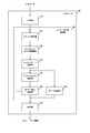
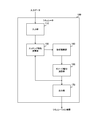
- FIG. 1 is a block diagram illustrating a configuration example of the simulator 100 according to the first embodiment.
- the simulator 100 is an apparatus that estimates etching characteristics (etching rate, polymer film thickness, damage) in dry etching, and includes an input unit 110, an etching characteristic calculation unit 150, and an output unit 170.
- the etching characteristic calculation unit 150 includes a flux calculation unit 151, a dangling bond rate calculation unit 152, an etching rate calculation unit 153, an outflux calculation unit 154, a polymer film thickness calculation unit 155, and a damage calculation unit 156.
- the simulator 100 is an example of an information processing apparatus described in the claims.
- the OS may be any of Windows (registered trademark), Linux (registered trademark), Unix (registered trademark), and Macintosh (registered trademark).
- the programming language may be C / C ++ (registered trademark), Fortran, JAVA (registered trademark), or the like.
- the input unit 110 inputs input data necessary for estimation of etching characteristics to the etching characteristic calculation unit 150 via a GUI (Graphical User Interface) or the like.
- input data for example, the processing initial conditions such as the type of etching gas, the flow rate of the etching gas, the pressure of the etching gas, the applied power, and the etching time are input.
- the flux calculation unit 151 calculates the amount of hydrogen in the etching gas that reacts with nitrogen in the workpiece as necessary. However, when an etching gas that does not contain hydrogen, such as a CF-based gas, is used, it is not necessary to calculate the hydrogen flux.
- the dangling bond ratio calculation unit 152 calculates a dangling bond ratio.
- the dangling bond ratio is the ratio of the area where the workpiece reacts with the etching gas to the area of the workpiece, and is also called the reaction area ratio.
- the workpiece includes a nitrogen compound such as Si 3 N 4, and the etching gas is, for example, a CF-based gas.
- the dangling bond rate is obtained by the following equations.
- Equation 1 ⁇ SiN is the surface density of Si 3 N 4 , and Y iSiN is the reaction probability of ions generated by ionization of the etching gas and Si 3 N 4 .
- the unit of areal density is, for example, cm ⁇ 2 .
- V net is the energy at a certain depth of ions.
- ⁇ (j, t) is the dangling bond rate at time t of the j-th slab.
- the unit of t is, for example, second.
- the slab indicates each layer in a slab model that divides a workpiece into a plurality of plate-like layers.
- ⁇ DB ER in Equation 1 is obtained by the following equation.
- ⁇ SiN is the film density of Si 3 N 4 .
- the unit of the film density is, for example, gram per cubic centimeter (g / cm ⁇ 3 ).
- ER (j, t) is an etching rate of the j-th slab at time t.
- the unit of the etching rate is, for example, centimeter per second (cm / s).
- the simulator 100 divides the workpiece into a plurality of slabs and calculates the dangling bond rate and the etching rate for each slab. However, even if the workpiece 100 is configured not to divide the workpiece into a plurality of slabs. Good.
- Y iSiN in Expression 1 is obtained by the following expression, for example.
- Y iSiN (V net ) 8.5 ⁇ 0.0073 ⁇ exp ⁇ 0.0023 ⁇ (E ⁇ E) ⁇ ⁇ 1.3 Equation 3
- Equation 3 E is ion energy.
- T is the film thickness of the polymer layer (protective film layer) generated by the primary reaction of the workpiece and the etching gas. In the initial state where the time t is “0”, the polymer layer is not formed, so an initial value such as “0” is set as the film thickness T. In the period of t> 0, the value calculated by the polymer film thickness calculator 155 is set as the film thickness T.
- the unit of the film thickness is, for example, centimeter (cm).
- ⁇ E in Equation 3 is obtained by the following equation.
- the dangling bond rate calculation unit 152 supplies the calculated dangling bond rate to the etching rate calculation unit 153 and the outflux calculation unit 154.
- the etching rate calculation unit 153 calculates an etching rate and obtains an estimated value thereof.
- the flux ⁇ F * of fluorine that reacts with Si 3 N 4 is obtained by the following equation.
- ⁇ F * (1 ⁇ Y HF ) ⁇ F Formula 5
- Y HF is the reaction probability between hydrogen and fluorine.
- ⁇ F is a fluorine flux incident on the processing surface.
- reaction probability Y FSiN between fluorine and Si 3 N 4 is obtained by the following equation.
- E is the energy of ions incident on the processing surface.
- Y FSiN (V net ) 0.0003 ⁇ exp ⁇ 0.0023 ⁇ (E ⁇ E) ⁇ ⁇ 1.3
- the etching rate of the j-th slab is, for example, Is calculated by In the above formula, ⁇ 1 is an index of the reaction product CF B1 .
- the etching rate calculation unit 153 supplies the calculated etching rate of the previous time step t-1 to the outflux calculation unit 154 and the damage calculation unit 156 as the outflux at time t.
- the outflux calculating unit 154 calculates the amount of nitrogen that reacts with carbon in the polymer layer. This nitrogen reacts secondarily with carbon to produce C 2 N 2 , and the C 2 N 2 volatilizes. For this reason, the amount of reacting nitrogen is treated as outflux that is volatilized and output to the outside of the workpiece.
- the outflux is calculated based on the etching rate from the etching rate calculation unit 153 and the dangling bond rate calculated by the dangling bond rate calculation unit 152, for example, by the following equation.
- ⁇ N ER is the outflux released from the workpiece.
- ⁇ H ** is the amount of hydrogen in the etching gas that reacts with nitrogen in the workpiece. When an etching gas that does not contain hydrogen, such as a CF-based gas, is used, ⁇ H ** is set to “0”.
- the outflux calculating unit 154 supplies the calculated outflux to the polymer film thickness calculating unit 155.
- the outflux calculating part 154 is an example of the flux calculating part as described in a claim.
- the polymer film thickness calculator 155 calculates the film thickness of the polymer film.
- an etching gas that does not contain hydrogen such as a CF-based gas
- the polymer film thickness T is obtained by the following equation based on outflux, for example.
- ⁇ p is the film density of the polymer film.
- Y CC is a reaction probability between carbon in the polymer film and carbon in the etching gas, and ⁇ C is a flux of carbon incident on the processing surface.
- Y OC1 is a reaction probability between carbon in the polymer film and oxygen in the etching gas, and ⁇ O is a flux of oxygen incident on the processing surface.
- Y FC is the reaction probability between fluorine in the etching gas and carbon in the polymer film.
- Y iC is the reaction probability between the incident ions and the carbon of the polymer film, and ⁇ i is the flux of the incident ions.
- ⁇ 1 is an input parameter for simulation of greater than 0 and less than or equal to 1. The higher this coefficient gamma 1 is small, the change of the polymer film quality, the reaction probability of the incident particles and carbon is low, indicates a low removal rate for removing volatile loss from the polymer layer.
- Y CN is the reaction probability between CH bonds in the polymer film and nitrogen in the outflux.
- the first term on the right side of Equation 10 indicates the amount of polymer layer deposited by etching
- the second term indicates that the polymer layer that reacts with oxygen and fluorine to volatilize is reduced.
- the third term indicates that carbon in the polymer film reacts with nitrogen to reduce the polymer layer.
- the left side is a value obtained by removing the volatilization amount of the second term and the third term from the deposition amount of the first term, and indicates the amount of polymer deposited.
- the polymer film thickness calculator 155 is an example of the protective film layer calculator described in the claims.
- the polymer film thickness calculation unit 155 supplies the calculated polymer film thickness to the output unit 170 and the dangling bond rate calculation unit 152.
- the damage calculation unit 156 calculates damage (crystal defects) according to the damage calculation method described in Patent Document 1.
- the damage calculation unit 156 is an example of a crystal defect calculation unit described in the claims.
- the output unit 170 outputs a simulation result. For example, the polymer film thickness, etching rate, damage, etc. for each time are output as simulation results. This simulation result may be visualized by GUI. The output and visualization of the simulation result may be performed when all the calculations are completed, or may be performed in real time during the calculation.
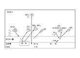
- FIG. 2 is a diagram for explaining the surface reaction model in the first embodiment.
- CHxFy in the etching gas reacts with the reaction layer in the workpiece containing silicon nitride (SiN) to react with silicon difluoride (SiF 2 ), silicon tetrafluoride (SiF 4 ), or hydrogen fluoride (HF). Is generated.
- CHxFy represents a CF-based gas or a CHF-based gas.
- a polymer layer containing carbon is deposited by the primary reaction of the etching gas and the reaction layer. Then, the polymer layer and a secondary fluorocarbon by the secondary reaction of the etching gas (CF 2) is generated.
- hydrocarbon CH
- hydrogen cyanide HCN
- carbon dinitride C 2 N 2
- CO Carbon monoxide
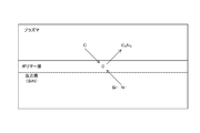
- FIG. 3 is a diagram for explaining a surface reaction model of the polymer layer in the first embodiment.
- CF-based gas When the CF-based gas is used, a polymer layer containing carbon is generated by etching. Then, the polymer layer and carbon in the etching gas react to generate carbon dinitride (C 2 N 2 ). As shown in the figure, when CF-based gas is used, it is not necessary to consider the reaction of hydrogen, so that “0” is set to ⁇ H ** in Equation 9.
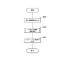
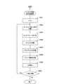
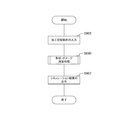
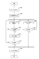
- FIG. 4 is a flowchart showing an example of the operation of the simulator 100 according to the first embodiment. This operation starts, for example, when a predetermined application for performing a simulation is executed.
- Input data such as machining initial conditions is input to the simulator 100 (step S902).
- the simulator 100 executes an etching characteristic calculation process for the workpiece (step S920). Then, the simulator 100 outputs a simulation result (step S907).
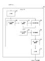
- FIG. 5 is a flowchart showing an example of the etching characteristic calculation process in the first embodiment.
- the simulator 100 sets an initial value (for example, “0”) at time t (step S921).
- the simulator 100 calculates the dangling bond rate (step S923) and calculates the etching rate (step S924). Further, damage is calculated based on the etching rate and the dangling bond rate (step S925). Then, the simulator 100 calculates outflux from the dangling bond rate and the etching rate (step S926). Further, the simulator 100 calculates the polymer film thickness from the outflux (step S928).
- the simulator 100 increases t for a certain time (step S929), and determines whether t has reached a preset end time (step S930). If t is not the end time (step S930: No), the simulator 100 returns to step S923. On the other hand, if t is the end time (step S930: Yes), the simulator 100 ends the etching characteristic calculation process.
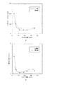
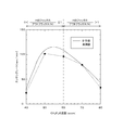
- FIG. 6 is a graph illustrating an example of the calculation result in the first embodiment.
- the vertical axis of a represents the etching rate
- the horizontal axis represents the flow rate of the C 4 H 8 etching gas.
- the solid line shows the locus of the etching rate obtained by the calculation
- the dotted line shows the locus of the actual measurement value measured by actually performing etching under the same conditions.
- the plasma monitoring data may further include IRLAS (Infrared-diodedioLaser Absorption Spectroscopy) data.
- the device type may be an ICP (Inductively Coupled Plasma) type, an ECR (Electron Cyclotron Resonance) type, or other plasma generation mechanism.
- the flux may be derived from a plasma simulation or a response surface function depending on process parameters (flow rate, pressure, gas type, power).
- the dangling bond rate and the etching rate were calculated every 0.01 seconds, for example. Further, the thickness of each slab was set to 0.5 nanometer (nm), and calculation was performed in the reaction layer, for example, to 14 slabs (that is, 7 nanometers in thickness). The polymer film thickness was calculated with the coefficient ⁇ 1 being 0.85. By repeating these calculations until the etching end time, the etching rate for each hour is obtained. As shown in a of FIG. 6, the calculation result can reproduce the tendency of the actual measurement value.
- the vertical axis of b in FIG. 6 indicates the etching rate selection ratio between silicon nitride and silicon dioxide, and the horizontal axis indicates the flow rate of the C 4 H 8 etching gas.
- the solid line indicates the trajectory of the selection ratio obtained by calculation, and the dotted line indicates the trajectory of the actual measurement value measured by actually performing etching under the same conditions. As shown in FIG. 5B, the selection ratio can also be reproduced.
- the amount of nitrogen that reacts with the polymer layer is obtained, and the volatile amount obtained from the amount of nitrogen is removed from the polymer layer to obtain the film thickness. Etching characteristics in etching of a workpiece containing nitrogen can be obtained accurately.
- Second Embodiment> In the first embodiment described above, it is assumed that an etching gas not containing hydrogen is used. However, an etching gas containing hydrogen such as a CHF-based gas can also be used.
- the simulator 100 of the second embodiment differs from the first embodiment in that the etching characteristics in etching with an etching gas containing hydrogen are estimated.
- FIG. 7 is a block diagram illustrating a configuration example of the simulator 100 according to the second embodiment.
- a CHF-based etching gas containing hydrogen is used.
- the flux calculation unit 151 according to the second embodiment is different from the first embodiment in that the flux of hydrogen is calculated.
- the flux calculation unit 151 calculates a hydrogen flux ⁇ H *** (hydrogen flux remaining after reaction with N, O, F) of hydrogen that reacts with the polymer layer among hydrogen in the etching gas.
- This flux ⁇ H *** is obtained by the following equations, for example.
- ⁇ H * (1 ⁇ Y HF ) ⁇ H Formula 13
- Equation 11 Y NH is the reaction probability between nitrogen and hydrogen.
- Y HO is the reaction probability between hydrogen and oxygen.
- Y HF is the reaction probability between hydrogen and fluorine.
- ⁇ H is a hydrogen flux incident on the processing surface.
- the flux calculation unit 151 supplies the calculated ⁇ H *** to the polymer film thickness calculation unit 155 and supplies ⁇ H ** to the outflux calculation unit 154.
- the outflux calculating unit 154 calculates the outflux according to Equation 9 based on ⁇ H ** from the flux calculating unit 151.
- the polymer film thickness calculator 155 of the second embodiment compares the hydrogen flux ⁇ H *** with the outflux ⁇ N ER, and calculates the polymer film thickness based on the comparison result. However, this is different from the first embodiment.
- the polymer film thickness can be obtained from Equation 10 as in the first embodiment.
- ⁇ H *** / ⁇ N ER is larger than “0” and equal to or smaller than “1”, that is, when the etching gas contains hydrogen and the hydrogen flux is equal to or smaller than the outflux, for example,
- the polymer film thickness is determined by the formula.
- Equation 14 Y HCN is the reaction probability between the CH bond and nitrogen in the polymer film, and Y CN is the reaction probability between carbon and nitrogen in the polymer film.
- ⁇ 2 is a simulation parameter greater than 0 and less than or equal to 1. It shows that the removal rate which removes the volatilization amount from a polymer layer is so low that this coefficient (gamma) 2 is small.
- the hydrogen flux When the hydrogen flux is less than or equal to the nitrogen outflux, the hydrogen reacts with fluorine on the polymer film surface and volatilizes as hydrogen fluoride. Further, the remaining hydrogen reacts with the incident oxygen and volatilizes as hydroxide (OH). The remaining hydrogen flux corresponds to ⁇ H ** in Equation 11. This hydrogen partially reacts with nitrogen, and the last remaining hydrogen forms an active C—H bond with carbon in the polymer film. Nitrogen acts on the hydrogen to form hydrogen cyanide (HCN) with the reaction probability Y HCN. Is formed and volatilizes. This volatilization amount corresponds to the third term on the right side of Equation 14.
- the polymer film thickness is calculated by the following equation: Is required.
- Equation 15 ⁇ 3 is a coefficient greater than 0 and less than or equal to 1. It shows that the removal rate which removes the volatilization amount from a polymer layer is so low that this coefficient (gamma) 3 is small.
- hydrogen flux When the hydrogen flux is greater than the outflux, hydrogen reacts with fluorine on the polymer film surface and volatilizes as hydrogen fluoride. Further, the remaining hydrogen reacts with the incident oxygen and volatilizes as hydroxide (OH). The remaining hydrogen flux corresponds to ⁇ H ** in Equation 11. This hydrogen partially reacts with nitrogen, and the last remaining hydrogen forms an active CH bond with carbon in the polymer film. When nitrogen acts there, hydrogen cyanide (HCN) is formed and volatilized with the reaction probability Y HCN . This volatilization amount corresponds to the third term on the right side of Equation 14. Nitrogen remaining in the reaction reacts with carbon in the polymer film to volatilize as carbon dinitride (C 2 N 2 ).
- C 2 N 2 carbon dinitride
- This volatilization amount corresponds to the fifth term on the right side of Equation 13.
- the remaining hydrogen finally reacts with carbon in the polymer film and volatilizes as hydrocarbon (CH).
- This volatilization amount corresponds to the fourth term on the right side of Equation 14.
- the polymer film thickness calculator 155 switches the formula for calculating the polymer film thickness in accordance with the ratio of the hydrogen flux to the outflux. Thereby, even when the ratio of the hydrogen flux to the outflux varies with time, an accurate polymer film thickness can be calculated. Thereby, the simulator 100 can calculate the etching characteristics with high accuracy.
- calculation formula is switched depending on the ratio of the hydrogen flux to the outflux, it is not limited to this configuration.
- requires the difference of these fluxes, and switches a calculation formula according to the difference may be sufficient.
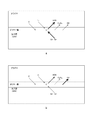
- FIG. 8 is a diagram for explaining a surface reaction model of a polymer film in the second embodiment.
- a in the figure is a figure for demonstrating the surface reaction model in case the flux of hydrogen is below an outflux.
- a CHF-based gas When a CHF-based gas is used, a polymer layer containing carbon is generated by etching. Then, hydrogen in the etching gas and the polymer layer react to generate hydrogen cyanide (HCN). Further, carbon dinitride (C 2 N 2 ) is generated by the reaction between the polymer layer and carbon in the etching gas. Furthermore, hydrogen in the etching gas reacts with the polymer layer to generate hydrocarbon (CH).
- CH hydrogen cyanide
- FIG. 8 is a diagram for explaining a surface reaction model when the hydrogen flux is larger than the nitrogen outflux.
- a polymer layer containing carbon is produced, producing hydrogen cyanide (HCN), carbon dinitride (C 2 N 2 ) and hydrocarbon (CH).
- HCN hydrogen cyanide
- C 2 N 2 carbon dinitride
- CH hydrocarbon
- the volatilization amount of hydrocarbon (CH) is particularly increased.
- FIG. 9 is a flowchart showing an example of the etching characteristic calculation process in the second embodiment.
- the etching characteristic calculation process of the second embodiment differs from that of the first embodiment in that steps S922 and S927 are further executed.
- the simulator 100 calculates hydrogen flux ⁇ H *** after initialization of t (step S921) (step S922).
- the simulator 100 executes steps S923 to S926, and compares the hydrogen flux ⁇ H *** with the outflux (step S927). Then, the simulator 100 calculates the polymer film thickness by a calculation formula corresponding to the comparison result (step S928).
- the simulator 100 increases t by a certain time (step S929), and determines whether t has reached the end time (step S930). If t is not the end time (step S930: No), the simulator 100 returns to step S922. On the other hand, if t is the end time (step S930: Yes), the simulator 100 ends the etching characteristic calculation process.
- FIG. 10 is a graph illustrating an example of a calculation result in the second embodiment.
- the vertical axis represents the etching rate
- the horizontal axis represents the flow rate of the etching gas of CH 2 F 2 which is a CHF-based gas.
- the solid line shows the locus of the etching rate obtained by the calculation
- the dotted line shows the locus of the actual measurement value measured by actually performing etching under the same conditions.
- the simulator 100 obtains etching characteristics in etching of the Si 3 N 4 film with a CHF-based gas.
- the combination of the etching gas and the workpiece is not limited as long as the etching gas, the polymer layer, and the workpiece contain at least carbon, hydrogen, and nitrogen.
- the simulator 100 may obtain the etching characteristics in etching of an organic film with N 2 / H 2 gas or a low dielectric constant (so-called Low-k) film.
- the following process / apparatus conditions are input.
- the amount of hydrogen and the amount of nitrogen are compared and the polymer film thickness is obtained based on the comparison result. Even when the value fluctuates, the polymer film thickness can be obtained accurately. Thereby, accurate etching characteristics can be obtained.
- the polymer film thickness, the etching rate, and the damage are obtained.
- the shape of the workpiece after the etching can be obtained from the etching rate.
- the simulator 100 according to the third embodiment is different from the second embodiment in that the shape of the workpiece after etching is further obtained.
- FIG. 11 is a block diagram illustrating a configuration example of the simulator 100 according to the third embodiment.
- the simulator 100 of the third embodiment is different from the second embodiment in that it further includes a shape calculation unit 160 and a damage distribution calculation unit 165.
- the shape calculation unit 160 estimates the shape of the workpiece after etching by calculation based on the etching rate.
- the shape is obtained, for example, by a voxel method in which a non-processed object is divided into a large number of cubic voxels and the progress of the shape is calculated in units of voxels.
- the shape calculation unit 160 supplies the calculation result to the damage distribution calculation unit 165.
- the damage distribution calculation unit 165 calculates damage distribution by the method described in Japanese Patent Application No. 2013-014556, for example.
- the damage distribution calculation unit 165 supplies the calculation result to the etching characteristic calculation unit 150 and the output unit 170.
- the damage calculation unit 156 and the shape calculation unit 160 are examples of the processing shape / crystal defect calculation unit described in the claims.
- the simulator 100 estimates the shape by the voxel method, but is not limited to this configuration.
- the simulator 100 may estimate the shape by, for example, a string method or a level set method instead of the voxel method.
- the calculation dimension may be two dimensions or three dimensions.
- FIG. 12 is a flowchart illustrating an example of the operation of the simulator 100 according to the third embodiment.
- the operation of the simulator 100 of the third embodiment is different from that of the second embodiment in that the shape / damage calculation process (step S930) is executed instead of the etching characteristic calculation process (step S920).
- FIG. 13 is a flowchart illustrating an example of a shape / damage calculation process according to the third embodiment. This shape / damage calculation process is the same as the damage calculation process of the second embodiment except that step S931 and step 932 are further executed.
- the simulator 100 calculates the shape of the workpiece (Step S931) after calculating the polymer film thickness (Step S928), distributes the damage (Step S932), and increases t for a certain time (Step S929).
- FIG. 14 is an example of a cross-sectional view of a workpiece before and after sidewall etching of a transistor according to the third embodiment.
- a is a sectional view before etching
- b in the figure is a sectional view after etching.
- the voxel size is, for example, 1 nanometer (nm).
- Polysilicon transistors were also used as workpieces. After processing a gate with a width of 60 nanometers and a height of 150 nanometers, a silicon dioxide film and a silicon nitride film are deposited, and assuming the etch-back process of the silicon nitride film, the shape after sidewall processing and the damage that occurs at that time A calculation of the distribution was made.
- the processing apparatus is a CCP etching apparatus, and the process conditions are as follows.
- the aperture ratio around the sidewall pattern is 100%.
- the aperture ratio is the ratio of the area to be etched to the surface area of the workpiece.
- the flux incident on the pattern with a radius of 20 millimeters was calculated including the redeposition effect of the reaction product on the pattern due to etching, taking into account the dependency of the chip level on the periphery of the target on the order of millimeters.
- the normal used for shape evolution after the etch rate was derived was derived from the flux vector using, for example, the method described in Japanese Patent Application Laid-Open No. 2014-29982.
- the etch rate and damage are calculated using this surface reaction model, the normal direction voxels are removed within the region corresponding to the etch rate, and the amount of damage is distributed to the surroundings until the etching is completed until the etching is completed. It was conducted. As a result, the shape / damage distribution indicated by b in FIG. 14 was obtained.
- the application pattern is not limited to the sidewall. It can be applied to various pattern processing such as masks and lenses.
- the simulator 100 calculates a two-dimensional shape, but may calculate a three-dimensional shape.
- the simulator 100 estimates the shape and damage of the workpiece after etching from the etching rate. Can be processed.
- the simulator 100 estimates the etching rate and the like while keeping the density of the etching gas, the ion energy distribution, the aperture ratio, and the like constant, but these may be further estimated.
- the simulator 100 of the fourth embodiment differs from the third embodiment in that the etching gas density, ion energy distribution, aperture ratio, and the like are further estimated.
- FIG. 15 is a block diagram illustrating a configuration example of the simulator 100 according to the fourth embodiment.
- the simulator 100 according to the fourth embodiment differs from the third embodiment in that it further includes a plasma state calculation unit 120, a sheath acceleration calculation unit 130, and an aperture ratio calculation unit 140.
- recipe information In the fourth embodiment, recipe information, apparatus information, calculation parameters, GDS (Graphic Data System) data, film thickness information, and the like are input as input data.
- GDS Graphic Data System
- the plasma state calculation unit 120 calculates parameters (such as gas density) indicating the plasma state.
- the plasma state calculation unit 120 calculates the density of each gas type (ion, radical, etc.) in the bulk plasma based on the initial conditions and supplies the calculation result to the sheath acceleration calculation unit 130.
- the calculation of the gas density is performed according to the procedure described in Japanese Patent No. 5397215, for example.
- the sheath acceleration calculation unit 130 calculates ion energy distribution and ion incident angle.
- the sheath acceleration calculation unit 130 determines the ion energy distribution as a final state accelerated in the sheath of ions generated by bulk plasma based on the gas density, gas pressure, and applied power, and the incident angle distribution on the pattern. Is calculated. These operations are performed, for example, according to the procedure described in M.J. Kushner, “Distribution” of “ion” energies “incident”, “electrodes” in “capacitively” coupled ”discharges,“ J. Appl. Phys. ”.
- the energy distribution of ions is expressed by, for example, an ion energy distribution function (IEDF: Ion Energy Distribution Function). Further, the ion incident angle is expressed by an ion incident angle distribution function (IADF: ion angular distribution function). A database obtained from actual measurement or the like may be used for these distribution functions.
- the sheath acceleration calculation unit 130 supplies the calculation result to the etching characteristic calculation unit 150.
- the aperture ratio calculation unit 140 calculates an aperture ratio.
- the aperture ratio calculation unit 140 calculates a wafer aperture ratio and a semilocal aperture ratio from GDS data, film thickness information, and the like.
- the wafer aperture ratio is the aperture ratio of the entire wafer when the wafer is a workpiece.
- the semilocal aperture ratio is an aperture ratio at a chip level formed on a wafer. The calculation of these aperture ratios is performed by the procedure described in Japanese Patent No. 5440021, for example.
- the aperture ratio calculation unit 140 supplies the calculation result to the etching characteristic calculation unit 150.
- the etching characteristic calculation unit 150 of the fourth embodiment calculates various fluxes such as out flux and incident flux based on the aperture ratio. Further, the etching characteristic calculation unit 150 of the fourth embodiment calculates the dangling bond rate and the etching rate based on the calculation result of the sheath acceleration calculation unit 130.
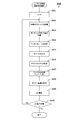
- FIG. 16 is a flowchart illustrating an example of the operation of the simulator 100 according to the fourth embodiment.
- the operation of the simulator 100 of the fourth embodiment is different from that of the first embodiment in that steps S903 to S905, S906, and S908 are further executed.
- the simulator 100 After inputting the processing initial conditions (step S902), the simulator 100 calculates the plasma state (step S903) and performs sheath acceleration calculation (step S904). Then, the simulator 100 calculates the aperture ratio (step S905) and executes shape / damage calculation processing (step S930).
- the simulator 100 compares the calculation result of the shape and damage with the required specification, and determines whether or not the difference from the specification is within a predetermined allowable range (step S906). If the difference from the spec is not within the allowable range (step S906: No), the simulator 100 changes the aperture ratio by arranging dummy patterns or the like (step S908), and returns to step S903. On the other hand, when the difference from the specification is within the allowable range (step S906: Yes), the simulator 100 outputs a simulation result (step S907) and ends the operation.
- This simulator 100 is used, for example, for layout design of semiconductor devices. For example, it is assumed that the desired specification of the width of the transistor sidewall is 60 nanomail ⁇ 10%. In this case, in step S908 of FIG. 16, a dummy pattern covered with a resist mask is arranged around the target processing. If the in-chip aperture ratio is reduced (or increased) by the arrangement of the dummy pattern, the amount of the reaction product from the mask re-incident on the pattern increases (or decreases). As a result, the sidewall width becomes larger (or smaller) and approaches the desired specification.
- process design and OPC (Optical Proximity Correction) design can be implemented in the same way by changing the correction factor from the dummy pattern arrangement to the process conditions and mask shape.
- the gas density, ion energy distribution, ion incident angle and aperture ratio are further calculated, and the etching characteristics are estimated from the calculation results. It can be carried out.
- the etching characteristics are estimated.
- the workpiece may be processed using the estimation result.
- the fifth embodiment is different from the fourth embodiment in that the workpiece is further processed using an estimation result such as an etching rate.
- FIG. 17 is an overall view showing an example of a manufacturing system according to the fifth embodiment.
- This manufacturing system manufactures a semiconductor device, and includes a simulator 100, a processing chamber 200, and a control device 300.
- the manufacturing system includes an FDC (Fault Detection & Classification) / EES (Equipment Engineering System) system 400.
- the apparatus including the simulator 100, the processing chamber 200, and the control device 300 is an example of a processing apparatus described in the claims.
- the processing chamber 200 is for processing a workpiece such as a semiconductor wafer.
- a CCP type apparatus is used as the processing chamber 200.
- OES, QMS, IRLAS, energy spectrum analyzer, and the like for acquiring input data necessary for simulation are mounted, and plasma is constantly monitored during processing.
- the sampling speed is, for example, 0.1 second (s).
- information acquired by these is transmitted to the simulator 100 together with processing conditions.
- the processing chamber 200 is an example of a processing unit described in the claims.
- the simulator 100 of the fifth embodiment has the same configuration as that of the above-described fourth embodiment.
- the simulator 100 calculates gas density, gas flux, ion energy distribution and incident angle distribution based on data from the processing chamber 200. If the calculation time is sufficiently shorter than the actual machining time, all may be obtained by reactor simulation. Furthermore, the simulator 100 calculates the aperture ratio using the GDS and the film thickness information, and calculates the shape and damage in consideration of the contribution of the aperture ratio to the flux.
- the aperture ratio and the flux generally have a linear relationship with each other.
- the simulator 100 changes the process parameters in the order of gas flow rate, gas pressure, applied power, and wafer temperature, and recalculates the desired specification. Find correction conditions that can be met.
- a desired specification for example, a sidewall width of 60 nanometers (nm) is set. In this case, for example, it is determined whether or not a tolerance of ⁇ 10% of the desired width is exceeded.
- the damage amount for example, it is determined whether or not it falls outside the allowable range of 50% of the desired amount.
- an apparatus other than the CCP type such as an ICP (Inductively Coupled Plasma) type or an ECR (Electron Cyclotron Resonance) type may be used as the processing chamber 200.
- ICP Inductively Coupled Plasma
- ECR Electro Cyclotron Resonance
- the simulator 100 When the simulator 100 finds the correction condition, the simulator 100 transmits the condition to the control device 300. On the other hand, when the correction condition is not found, the simulator 100 generates an alert signal and transmits it to the FDC / EES system 400.
- the simulator 100 When the calculation time is equal to or longer than the actual machining time, the simulator 100 does not calculate the shape or damage during machining, but calculates the shape and damage in advance and saves them in a database or the like before machining. It may be. In this case, the processing chamber 200 may perform processing using the database.
- the control device 300 is for controlling the processing chamber 200.
- the control device 300 changes the process parameter of the processing chamber 200 based on the correction condition obtained by the simulator 100.
- the control device 300 is an example of a control unit described in the claims.
- the FDC / ESS system 400 performs quality control of semiconductor devices.
- the FDC / EES system 400 receives an alert signal from the simulator 100, the FDC / ESS system 400 stops the entire manufacturing system.
- an image sensor, a drive circuit, a signal processing circuit, and the like are manufactured by such a manufacturing system.
- an electronic apparatus such as an imaging apparatus is manufactured from these devices.
- FIG. 18 is a flowchart showing an example of the operation of the manufacturing system according to the fifth embodiment.
- a wafer lot is set in the processing chamber 200 by a transfer robot or an operator (step S901), and an initial processing condition (process recipe) is input automatically by an operator directly or by an apparatus function (step S902). ).
- the processing step is, for example, sidewall processing of a gate in polysilicon having a film thickness of 150 nanometers.
- the following conditions are input as the processing initial conditions. Wafer aperture ratio: 45% SiN etching: main etching step CF 4 gas: 200 sccm O 2 gas: 5 sccm CHF 3 gas: 100 sccm Source power: 700 Watts (W) Bias power: 400 watts (W) Pressure: 40 mTorr (mTorr) SiN etching: Over etching step CF 3 gas: 150 sccm O 2 gas: 100 sccm Ar gas: 500 sccm Source power: 500 Watts (W) Bias power: 300 watts (W) Pressure: 50 mTorr (mTorr)
- the simulator 100 executes shape / damage calculation processing (step S930). Then, the simulator 100 compares the calculation result with the desired specification and determines whether or not process correction is necessary (step S911). If process correction is necessary (step S911: Yes), the control device 300 corrects the process (step S912).
- step S911: Yes the simulator 100 determines whether or not the current time is the etching end time (step S913). If it is not the end time (step S913: No), the simulator 100 returns to step S930. If it is the end time (step S913: Yes), the simulator 100 stops the operation.
- the processing chamber 200 performs etching in the chamber (step S914), and determines whether or not the current time is the etching end time (step S915). If it is not the end time (step S914: No), the processing chamber 200 returns to step S914. If it is the end time (step S914: Yes), the processing chamber 200 stops the etching operation.
- step S916 After the operation of the simulator 100 and the processing chamber 200 is stopped, the wafer lot is collected by the transfer robot or the worker (step S916). After step S916, the manufacturing operation ends.
- the manufacturing system performs processing by plasma etching, but is not limited to plasma etching as long as it is a semiconductor processing using plasma.
- the manufacturing system may perform processing by, for example, CVD (Chemical Vapor Deposition) or PVD (Physical Vapor Deposition).
- the manufacturing system etches the workpiece based on the estimation result of the etching characteristics, the workpiece can be machined with high accuracy.
- the processing procedure described in the above embodiment may be regarded as a method having a series of these procedures, and a program for causing a computer to execute these series of procedures or a recording medium storing the program. You may catch it.
- a recording medium for example, a CD (Compact Disc), an MD (MiniDisc), a DVD (Digital Versatile Disc), a memory card, a Blu-ray disc (Blu-ray (registered trademark) Disc), or the like can be used.
- a flux calculation procedure in which an information processing apparatus calculates a plurality of fluxes in a surface reaction model in which a processing surface of a workpiece includes a protective film layer and a reaction layer; The information processing apparatus calculates the removal term according to a comparison result of the plurality of fluxes in an arithmetic expression for calculating the thickness of the protective film layer after etching based on a removal term describing the removal of the protective film layer.
- An etching characteristic estimation method comprising: a protective film layer calculation procedure for switching and calculating the thickness of the protective film layer.
- (9) a flux calculation procedure in which the information processing apparatus calculates a plurality of fluxes in a surface reaction model in which a processing surface of a workpiece includes a protective film layer and a reaction layer;
- the information processing apparatus calculates the removal term according to a comparison result of the plurality of fluxes in an arithmetic expression for calculating the thickness of the protective film layer after etching based on a removal term describing the removal of the protective film layer.
- a flux calculation unit that calculates a plurality of fluxes in a surface reaction model in which the processing surface of the workpiece includes a protective film layer and a reaction layer;
- the protective film layer is switched according to the comparison result of the plurality of fluxes in the arithmetic expression.
- An information processing apparatus comprising a protective film layer calculation unit that calculates the thickness of the film.
- the information processing apparatus calculates the removal term according to a comparison result of the plurality of fluxes in an arithmetic expression for calculating the thickness of the protective film layer after etching based on a removal term describing the removal of the protective film layer.
- the information processing apparatus includes a design procedure for performing at least one of a semiconductor device processing process, OPC (Optical Proximity Correction) design, and layout design based on a calculation result in the processing shape / crystal defect calculation procedure. Design method.
- a flux calculation unit that calculates a plurality of fluxes;
- the protective film layer is switched according to the comparison result of the plurality of fluxes in the arithmetic expression.
- a protective film layer calculation unit for calculating the thickness of A processing unit for processing the workpiece according to processing conditions of the workpiece;
- a plasma state calculation unit for calculating a plasma density used for etching the workpiece based on the processing conditions;
- a machining shape / crystal defect computing unit that computes at least one variation of the machining shape and crystal defects of the workpiece based on the computation result of the plasma state computing unit and the thickness of the protective film layer,
- a control unit that changes the processing condition based on the calculation result of the processing shape / crystal defect calculation unit,
- a processing apparatus comprising: (13) In a surface reaction model in which the processing surface of the workpiece includes a protective film layer and a reaction layer, the information processing apparatus calculates a plurality of fluxes; The information processing apparatus calculates the removal term according to a comparison result of the plurality of fluxes in an arithmetic expression for calculating the thickness of the protective film layer after etching based on a removal term describing the removal of the protective film layer.
- a protective film layer calculation unit that switches and calculates the thickness of the protective film layer;
- a processing procedure for processing the workpiece according to the processing conditions of the workpiece, A plasma state calculation procedure in which the information processing apparatus calculates a density of plasma used for etching the workpiece based on the processing conditions;
- a processing shape / crystal defect calculation procedure in which the information processing device calculates at least one variation of a processing shape of the workpiece and a crystal defect based on a calculation result of the plasma state calculation unit and a thickness of the protective film layer
- a control method in which a control part comprises a control procedure which changes the processing conditions based on a calculation result of the processing shape and crystal defect calculation procedure.
Landscapes
- Engineering & Computer Science (AREA)
- Physics & Mathematics (AREA)
- Computer Hardware Design (AREA)
- General Physics & Mathematics (AREA)
- Chemical & Material Sciences (AREA)
- Microelectronics & Electronic Packaging (AREA)
- Theoretical Computer Science (AREA)
- Condensed Matter Physics & Semiconductors (AREA)
- Manufacturing & Machinery (AREA)
- Power Engineering (AREA)
- Evolutionary Computation (AREA)
- Inorganic Chemistry (AREA)
- General Chemical & Material Sciences (AREA)
- Chemical Kinetics & Catalysis (AREA)
- General Engineering & Computer Science (AREA)
- Geometry (AREA)
- Medical Informatics (AREA)
- Software Systems (AREA)
- Automation & Control Theory (AREA)
- Computer Vision & Pattern Recognition (AREA)
- Artificial Intelligence (AREA)
- Health & Medical Sciences (AREA)
- Drying Of Semiconductors (AREA)
Priority Applications (1)
| Application Number | Priority Date | Filing Date | Title |
|---|---|---|---|
| US15/327,731 US10403516B2 (en) | 2014-07-30 | 2015-06-15 | Etching characteristic estimation method, program, information processing apparatus, processing apparatus, designing method, and production method |
Applications Claiming Priority (2)
| Application Number | Priority Date | Filing Date | Title |
|---|---|---|---|
| JP2014154811A JP6117746B2 (ja) | 2014-07-30 | 2014-07-30 | エッチング特性推定方法、プログラム、情報処理装置、加工装置、設計方法、および、製造方法 |
| JP2014-154811 | 2014-07-30 |
Publications (1)
| Publication Number | Publication Date |
|---|---|
| WO2016017303A1 true WO2016017303A1 (ja) | 2016-02-04 |
Family
ID=55217208
Family Applications (1)
| Application Number | Title | Priority Date | Filing Date |
|---|---|---|---|
| PCT/JP2015/067141 Ceased WO2016017303A1 (ja) | 2014-07-30 | 2015-06-15 | エッチング特性推定方法、プログラム、情報処理装置、加工装置、設計方法、および、製造方法 |
Country Status (3)
| Country | Link |
|---|---|
| US (1) | US10403516B2 (enExample) |
| JP (1) | JP6117746B2 (enExample) |
| WO (1) | WO2016017303A1 (enExample) |
Families Citing this family (3)
| Publication number | Priority date | Publication date | Assignee | Title |
|---|---|---|---|---|
| JP7166966B2 (ja) | 2019-03-15 | 2022-11-08 | 株式会社Screenホールディングス | 処理条件選択方法、基板処理方法、基板製品製造方法、処理条件選択装置、コンピュータープログラム、および、記憶媒体 |
| TW202509802A (zh) * | 2023-03-30 | 2025-03-01 | 日商東京威力科創股份有限公司 | 電腦程式、資訊處理方法及資訊處理裝置 |
| CN119148540B (zh) * | 2024-11-15 | 2025-03-07 | 深圳市荣强科技有限公司 | 基于多层次因素的表面活性剂工艺参数分析方法及系统 |
Citations (3)
| Publication number | Priority date | Publication date | Assignee | Title |
|---|---|---|---|---|
| WO2011115023A1 (ja) * | 2010-03-16 | 2011-09-22 | みずほ情報総研株式会社 | プラズマプロセスによる加工形状の予測システム、方法及びプログラム |
| JP2012186394A (ja) * | 2011-03-07 | 2012-09-27 | Mizuho Information & Research Institute Inc | プラズマ加工形状シミュレーション装置及びプログラム |
| JP2014029982A (ja) * | 2012-06-28 | 2014-02-13 | Sony Corp | シミュレーション方法、シミュレーションプログラム、加工装置およびシミュレータ |
Family Cites Families (2)
| Publication number | Priority date | Publication date | Assignee | Title |
|---|---|---|---|---|
| JP2008053507A (ja) * | 2006-08-25 | 2008-03-06 | Matsushita Electric Ind Co Ltd | ドライエッチング方法 |
| JP5732843B2 (ja) | 2010-12-21 | 2015-06-10 | ソニー株式会社 | シミュレータ、加工装置、ダメージ評価方法、及び、ダメージ評価プログラム |
-
2014
- 2014-07-30 JP JP2014154811A patent/JP6117746B2/ja active Active
-
2015
- 2015-06-15 US US15/327,731 patent/US10403516B2/en active Active
- 2015-06-15 WO PCT/JP2015/067141 patent/WO2016017303A1/ja not_active Ceased
Patent Citations (3)
| Publication number | Priority date | Publication date | Assignee | Title |
|---|---|---|---|---|
| WO2011115023A1 (ja) * | 2010-03-16 | 2011-09-22 | みずほ情報総研株式会社 | プラズマプロセスによる加工形状の予測システム、方法及びプログラム |
| JP2012186394A (ja) * | 2011-03-07 | 2012-09-27 | Mizuho Information & Research Institute Inc | プラズマ加工形状シミュレーション装置及びプログラム |
| JP2014029982A (ja) * | 2012-06-28 | 2014-02-13 | Sony Corp | シミュレーション方法、シミュレーションプログラム、加工装置およびシミュレータ |
Also Published As
| Publication number | Publication date |
|---|---|
| JP2016032064A (ja) | 2016-03-07 |
| JP6117746B2 (ja) | 2017-04-19 |
| US10403516B2 (en) | 2019-09-03 |
| US20170207107A1 (en) | 2017-07-20 |
Similar Documents
| Publication | Publication Date | Title |
|---|---|---|
| KR100847368B1 (ko) | 식각 선택도를 제어하기 위한 방법 및 장치 | |
| CN105493255B (zh) | 用于横向裁剪硬掩模的方法 | |
| TWI661323B (zh) | 模擬方法,模擬程式,製程控制系統,模擬器,製程設計方法及光罩設計方法 | |
| JP6177671B2 (ja) | シミュレーション方法、シミュレーションプログラムおよびシミュレータ | |
| JP5732843B2 (ja) | シミュレータ、加工装置、ダメージ評価方法、及び、ダメージ評価プログラム | |
| JP6781689B2 (ja) | 情報処理装置、加工装置、推定方法、プログラム、および、加工方法 | |
| JP7566099B2 (ja) | 基板処理方法および基板処理装置 | |
| CN103809462A (zh) | 模拟方法及程序、模拟器、加工设备和制造半导体装置的方法 | |
| CN103514318A (zh) | 模拟方法、计算机可读介质、处理装置及模拟器 | |
| JP6117746B2 (ja) | エッチング特性推定方法、プログラム、情報処理装置、加工装置、設計方法、および、製造方法 | |
| JP2010199126A (ja) | プラズマ処理方法およびプラズマ処理装置 | |
| KR20180034698A (ko) | 실리콘 함유 기판의 에칭 방법 | |
| Kuboi et al. | Modeling and simulation of plasma-induced damage distribution during hole etching of SiO2 over Si substrate by fluorocarbon plasma | |
| US10204832B2 (en) | Method of patterning intersecting structures | |
| US10529582B2 (en) | Plasma etching method and method of fabricating semiconductor device | |
| CN105336663B (zh) | 金属互连结构的形成方法 | |
| JP3913145B2 (ja) | パターン形成方法 | |
| KR20120026255A (ko) | 반도체 소자의 형성 방법 | |
| US9953886B2 (en) | Single-wafer real-time etch rate and uniformity predictor for plasma etch processes | |
| CN112786436A (zh) | 半导体结构及其形成方法 | |
| JP2013089827A (ja) | 半導体装置の製造方法 | |
| JP2007193037A (ja) | フォトマスクの製造方法 | |
| TW202501653A (zh) | 半導體裝置的計測方法,半導體裝置的計測系統及顯示裝置 |
Legal Events
| Date | Code | Title | Description |
|---|---|---|---|
| 121 | Ep: the epo has been informed by wipo that ep was designated in this application |
Ref document number: 15826772 Country of ref document: EP Kind code of ref document: A1 |
|
| WWE | Wipo information: entry into national phase |
Ref document number: 15327731 Country of ref document: US |
|
| NENP | Non-entry into the national phase |
Ref country code: DE |
|
| 122 | Ep: pct application non-entry in european phase |
Ref document number: 15826772 Country of ref document: EP Kind code of ref document: A1 |