WO2016017203A1 - 超電導線材 - Google Patents
超電導線材 Download PDFInfo
- Publication number
- WO2016017203A1 WO2016017203A1 PCT/JP2015/057641 JP2015057641W WO2016017203A1 WO 2016017203 A1 WO2016017203 A1 WO 2016017203A1 JP 2015057641 W JP2015057641 W JP 2015057641W WO 2016017203 A1 WO2016017203 A1 WO 2016017203A1
- Authority
- WO
- WIPO (PCT)
- Prior art keywords
- substrate
- superconducting wire
- superconducting
- layer
- material layer
- Prior art date
- Legal status (The legal status is an assumption and is not a legal conclusion. Google has not performed a legal analysis and makes no representation as to the accuracy of the status listed.)
- Ceased
Links
Images



Classifications
-
- H—ELECTRICITY
- H01—ELECTRIC ELEMENTS
- H01B—CABLES; CONDUCTORS; INSULATORS; SELECTION OF MATERIALS FOR THEIR CONDUCTIVE, INSULATING OR DIELECTRIC PROPERTIES
- H01B12/00—Superconductive or hyperconductive conductors, cables, or transmission lines
- H01B12/02—Superconductive or hyperconductive conductors, cables, or transmission lines characterised by their form
- H01B12/06—Films or wires on bases or cores
-
- C—CHEMISTRY; METALLURGY
- C01—INORGANIC CHEMISTRY
- C01F—COMPOUNDS OF THE METALS BERYLLIUM, MAGNESIUM, ALUMINIUM, CALCIUM, STRONTIUM, BARIUM, RADIUM, THORIUM, OR OF THE RARE-EARTH METALS
- C01F17/00—Compounds of rare earth metals
- C01F17/30—Compounds containing rare earth metals and at least one element other than a rare earth metal, oxygen or hydrogen, e.g. La4S3Br6
- C01F17/32—Compounds containing rare earth metals and at least one element other than a rare earth metal, oxygen or hydrogen, e.g. La4S3Br6 oxide or hydroxide being the only anion, e.g. NaCeO2 or MgxCayEuO
-
- C—CHEMISTRY; METALLURGY
- C01—INORGANIC CHEMISTRY
- C01G—COMPOUNDS CONTAINING METALS NOT COVERED BY SUBCLASSES C01D OR C01F
- C01G1/00—Methods of preparing compounds of metals not covered by subclasses C01B, C01C, C01D, or C01F, in general
-
- C—CHEMISTRY; METALLURGY
- C01—INORGANIC CHEMISTRY
- C01G—COMPOUNDS CONTAINING METALS NOT COVERED BY SUBCLASSES C01D OR C01F
- C01G3/00—Compounds of copper
-
- H—ELECTRICITY
- H01—ELECTRIC ELEMENTS
- H01B—CABLES; CONDUCTORS; INSULATORS; SELECTION OF MATERIALS FOR THEIR CONDUCTIVE, INSULATING OR DIELECTRIC PROPERTIES
- H01B12/00—Superconductive or hyperconductive conductors, cables, or transmission lines
- H01B12/14—Superconductive or hyperconductive conductors, cables, or transmission lines characterised by the disposition of thermal insulation
-
- H—ELECTRICITY
- H01—ELECTRIC ELEMENTS
- H01F—MAGNETS; INDUCTANCES; TRANSFORMERS; SELECTION OF MATERIALS FOR THEIR MAGNETIC PROPERTIES
- H01F6/00—Superconducting magnets; Superconducting coils
- H01F6/06—Coils, e.g. winding, insulating, terminating or casing arrangements therefor
-
- H—ELECTRICITY
- H10—SEMICONDUCTOR DEVICES; ELECTRIC SOLID-STATE DEVICES NOT OTHERWISE PROVIDED FOR
- H10N—ELECTRIC SOLID-STATE DEVICES NOT OTHERWISE PROVIDED FOR
- H10N60/00—Superconducting devices
- H10N60/01—Manufacture or treatment
- H10N60/0268—Manufacture or treatment of devices comprising copper oxide
- H10N60/0801—Manufacture or treatment of filaments or composite wires
-
- H—ELECTRICITY
- H10—SEMICONDUCTOR DEVICES; ELECTRIC SOLID-STATE DEVICES NOT OTHERWISE PROVIDED FOR
- H10N—ELECTRIC SOLID-STATE DEVICES NOT OTHERWISE PROVIDED FOR
- H10N60/00—Superconducting devices
- H10N60/20—Permanent superconducting devices
- H10N60/203—Permanent superconducting devices comprising high-Tc ceramic materials
-
- C—CHEMISTRY; METALLURGY
- C01—INORGANIC CHEMISTRY
- C01P—INDEXING SCHEME RELATING TO STRUCTURAL AND PHYSICAL ASPECTS OF SOLID INORGANIC COMPOUNDS
- C01P2006/00—Physical properties of inorganic compounds
- C01P2006/40—Electric properties
-
- Y—GENERAL TAGGING OF NEW TECHNOLOGICAL DEVELOPMENTS; GENERAL TAGGING OF CROSS-SECTIONAL TECHNOLOGIES SPANNING OVER SEVERAL SECTIONS OF THE IPC; TECHNICAL SUBJECTS COVERED BY FORMER USPC CROSS-REFERENCE ART COLLECTIONS [XRACs] AND DIGESTS
- Y02—TECHNOLOGIES OR APPLICATIONS FOR MITIGATION OR ADAPTATION AGAINST CLIMATE CHANGE
- Y02E—REDUCTION OF GREENHOUSE GAS [GHG] EMISSIONS, RELATED TO ENERGY GENERATION, TRANSMISSION OR DISTRIBUTION
- Y02E40/00—Technologies for an efficient electrical power generation, transmission or distribution
- Y02E40/60—Superconducting electric elements or equipment; Power systems integrating superconducting elements or equipment
Definitions
- This invention relates to a superconducting wire, and more particularly to a superconducting wire having a superconducting material layer formed on a substrate.
- Such an oxide superconducting wire generally has an intermediate layer formed on an oriented metal substrate, an oxide superconducting material layer formed on the intermediate layer, and silver (Ag) or copper (Cu ) Stabilization layer (see, for example, JP-A-2013-12406 (Patent Document 1)).
- the superconducting wire having the above-described configuration is wound into, for example, a coil to form a superconducting coil.
- the surface of the wound superconducting wire (particularly the stabilization layer surface on which the superconducting material layer is formed) is in contact with the superconducting wire or other member laminated on the surface, and the surface is There was a case where it was damaged.
- the superconducting material layer of the superconducting wire is also damaged due to the damage, and as a result, the characteristics of the superconducting wire may be deteriorated.
- the present invention has been made to solve the above-described problems, and an object of the present invention is to provide a superconducting wire capable of suppressing deterioration of superconducting characteristics.
- the superconducting wire includes a laminate and a coating layer.
- the laminate includes a substrate having a main surface and a superconducting material layer formed on the main surface.
- the covering layer is disposed at least on the superconducting material layer.
- the surface portion located on the superconducting material layer has a concave shape.
- the surface portion of the coating layer of the superconducting wire has a concave shape, it is possible to reduce the possibility that other members stacked on the surface portion come into contact with the recessed region of the surface portion. For this reason, the deterioration of the superconducting characteristics due to the contact can be suppressed.
- FIG. 3 is a flowchart showing a method for manufacturing a superconducting wire according to the first embodiment.
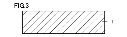
- FIG. 3 is a schematic cross-sectional view for illustrating the method for manufacturing the superconducting wire according to the first embodiment.
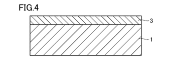
- FIG. 3 is a schematic cross-sectional view for illustrating the method for manufacturing the superconducting wire according to the first embodiment.
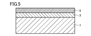
- FIG. 3 is a schematic cross-sectional view for illustrating the method for manufacturing the superconducting wire according to the first embodiment.
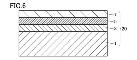
- FIG. 3 is a schematic cross-sectional view for illustrating the method for manufacturing the superconducting wire according to the first embodiment.
- a superconducting wire 10 (see FIG. 1) according to one embodiment of the present invention includes a laminate 20 and a coating layer (stabilization layer 9 or protective layer 7).
- the stacked body 20 includes a substrate 1 having a main surface and a superconducting material layer 5 formed on the main surface.
- the covering layer (stabilizing layer 9 or protective layer 7) is disposed on at least the superconducting material layer 5.
- the surface portion (surface portion 25 of stabilizing layer 9 or the upper surface of protective layer 7) located on superconducting material layer 5 has a concave shape.
- the superconducting material layer 5 can be formed directly on the main surface of the substrate 1 or indirectly via the intermediate layer 3 or the like.
- the surface portion of the coating layer (stabilization layer 9 or protective layer 7) of the superconducting wire 10 has a concave shape, another member (for example, the superconducting wire 10 is laminated on the surface portion).
- the other part or the like contacts the recessed area of the surface part 25 can be reduced. For this reason, since possibility that the superconducting material layer 5 will be damaged due to the said contact can be reduced, deterioration of the superconducting characteristic in the superconducting wire 10 can be suppressed.
- the distance L1 in the thickness direction of the substrate between the top portion 21 and the bottom portion 23 of the concave portion of the surface portion 25 in the cross section in the width direction of the substrate 1 is 1 ⁇ m. It may be 100 ⁇ m or less. In this case, it is possible to reduce the possibility that another member or the like will come into contact with the concave surface portion 25, so that the possibility of breakage of the superconducting material layer 5 described above can be reliably reduced.
- the top portion 21 means a region farthest from the superconducting material layer 5 (for example, a region protruding in a convex shape) in the surface portion 25 having a concave shape.
- the bottom portion 23 refers to a region closest to the superconducting material layer 5 in the surface portion 25 (for example, a deepest region inside the concave shape). If the distance L1 is less than 1 ⁇ m, the concave shape of the surface portion 25 does not have a sufficient depth, and the above-described effects cannot be exhibited sufficiently. Further, when the distance L1 exceeds 100 ⁇ m, the top portion 21 of the surface portion 25 protrudes too much, and there is a high possibility that the top portion 21 is damaged.
- the lower limit of the distance L1 is preferably 5 ⁇ m, more preferably 10 ⁇ m, and even more preferably 15 ⁇ m.
- the upper limit of the distance L1 is preferably 80 ⁇ m, more preferably 70 ⁇ m, and even more preferably 50 ⁇ m.
- the width W1 of the surface portion 25 in the cross section in the width direction of the substrate 1 is the region (back surface portion 26) located on the opposite side of the surface portion in the superconducting wire. It may be narrower than the width W2.
- the superconducting wire 10 is wound to form a coil or the like, between the portion of the superconducting wire 10 on the outer peripheral side and the other portion located on the inner peripheral side of the portion of the superconducting wire 10. A gap can be formed. For this reason, the possibility that the surface portion 25 of the laminated superconducting wire 10 is damaged by other portions of the superconducting wire 10 laminated can be reduced.
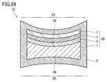
- the shape of the back surface portion 26 located on the opposite side of the front surface portion 25 in the superconducting wire 10 is either a flat shape (for example, see FIG. 1) or a concave shape (for example, see FIG. 29). There may be.
- the back surface portion 26 is directly on the central portion (for example, a concave bottom portion). Can be prevented from touching.
- the shape of the back surface portion 26 located on the opposite side of the surface portion 25 in the superconducting wire 10 may be a convex curved surface.
- the shape of the surface portion 25 may be a concave curved surface.
- the curvature radius of the back surface portion 26 may be larger than the curvature radius of the front surface portion 25. In this case, since the curvature radii of the front surface portion 25 and the back surface portion 26 are different when the superconducting wire 10 is stacked, it is possible to prevent the back surface portion 26 from coming into direct contact with the central portion of the front surface portion 25 and the like.
- the superconducting material layer 5 has a thickness T1 of the coating layer (stabilizing layer 9) on the central portion of the superconducting material layer 5 in the cross section in the width direction of the substrate 1.
- the thickness T2 of the coating layer (stabilizing layer 9) on the end of the substrate may be thicker.
- the top in the concave shape of the surface portion 25 of the coating layer is a region on the end of the superconducting material layer 5.
- region of the coating layer on the edge part of the said superconducting material layer 5 becomes high possibility that it will contact directly with another member (For example, other part of the superconducting wire 10 laminated
- the thickness T2 of the coating layer in the region where the other member is in contact is sufficiently thick. The possibility that the resulting pressure adversely affects the superconducting material layer 5 can be reduced.
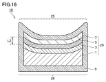
- a superconducting wire 10 (see FIG. 16) according to an aspect of the present invention includes a substrate 1 having a main surface and a superconducting material layer 5 formed on the main surface.
- the surface of the superconducting material layer 5 has a concave shape.
- the upper surface (surface portion 25) of the coating layer is easily made concave. be able to.
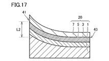
- the distance L2 in the thickness direction of the substrate 1 may be 1 ⁇ m or more and 100 ⁇ m or less.
- the value of the internal stress due to the concave shape of the surface in the superconducting material layer 5 can be suppressed to a level that does not adversely affect the superconducting characteristics, and on the surface of the superconducting material layer 5 (see FIG. 16).
- the upper surface of the coating layer to be formed can be surely made concave.
- the top 41 is a region farthest from the back surface of the substrate 1 (the back surface opposite to the surface on which the superconducting material layer 5 is formed) on the surface of the concave superconducting material layer 5 (for example, Means a region protruding in a convex shape.
- the bottom 43 refers to a region closest to the back surface of the substrate 1 on the surface of the superconducting material layer 5 (for example, a deepest region inside the concave shape).
- the lower limit of the distance L2 is preferably 5 ⁇ m, more preferably 10 ⁇ m, and even more preferably 15 ⁇ m.
- the upper limit of the distance L2 is preferably 80 ⁇ m, more preferably 70 ⁇ m, and even more preferably 50 ⁇ m.
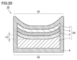
- a superconducting wire 10 (see FIG. 20) according to an aspect of the present invention includes a substrate 1 having a main surface and a superconducting material layer 5 formed on the main surface.
- the main surface 55 (see FIG. 18) of the substrate 1 has a concave shape.
- the upper surface (surface portion 25) of the coating layer can be easily formed. It can be a concave shape. As a result, it is possible to reduce the possibility that other members (for example, other portions of the superconducting wire 10) stacked on the upper surface come into contact with the recessed region of the surface portion 25.
- the distance L3 in the thickness direction of the substrate 1 may be 1 ⁇ m or more and 100 ⁇ m or less.
- the value of the internal stress generated due to the concave shape of the main surface 55 is set to a level at which no adverse effect on the superconducting characteristics occurs.
- the upper surface of the coating layer formed on the surface of the superconducting material layer 5 can be surely made concave.
- the top portion 51 is a region (for example, a convex shape) that is farthest from the back surface of the substrate 1 (the back surface opposite to the surface on which the superconducting material layer 5 is formed) on the surface of the substrate 1 having a concave shape. Or the thickest region of the substrate 1 on the main surface of the substrate 1).
- the bottom 53 is a region closest to the back surface of the substrate 1 on the surface of the substrate 1 (for example, a deepest region inside the concave shape or a portion where the thickness of the substrate 1 is the thinnest in the main surface 55 of the substrate 1). .
- the distance L3 is less than 1 ⁇ m, the concave shape of the surface portion 25 of the covering layer (stabilizing layer 9) formed on the surface of the laminate 20 including the main surface 55 of the substrate 1 and the superconducting material layer 5 is sufficient. However, the above-described effects cannot be exhibited sufficiently. Further, when the distance L3 exceeds 100 ⁇ m, an excessive internal stress may be generated in the superconducting material layer 5 formed on the main surface 55 of the substrate 1, and as a result, the superconducting characteristics may be deteriorated. .
- the lower limit of the distance L3 is preferably 5 ⁇ m, more preferably 10 ⁇ m, and even more preferably 15 ⁇ m.
- the upper limit of the distance L3 is preferably 80 ⁇ m, more preferably 70 ⁇ m, and even more preferably 50 ⁇ m.
- the width W3 of the main surface 55 is a region located on the opposite side of the main surface 55 in the substrate 1 in the cross section in the width direction of the substrate 1 ( It may be narrower than the width W4 of the back surface 56) in FIG.
- the superconducting wire 10 is wound to form a coil or the like, between the portion of the superconducting wire 10 on the outer peripheral side and the other portion located on the inner peripheral side of the portion of the superconducting wire 10. A gap can be formed.
- the back surface 56 located on the opposite side of the main surface 55 (see FIG. 18 or 27) on the substrate 1 has a planar shape (see FIG. 18) and Any one of the concave shapes (see FIG. 27) may be used.
- the back surface portion 26 is in direct contact with the central portion (for example, a concave bottom portion) of the front surface portion 25 that has a concave shape along the shape of the main surface 55. Can be prevented.
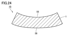
- the shape of the back surface 56 (see FIG. 24) located on the opposite side of the main surface 55 (see FIG. 24) on the substrate 1 is a convex curved surface.
- the shape of the main surface 55 may be a concave curved surface.
- the curvature radius of the back surface 56 may be larger than the curvature radius of the main surface 55.
- the surface (surface portion 25) of superconducting wire 10 located on the main surface 55 side of substrate 1 and the superconducting wire located on the back surface 56 side of substrate 1 are overlapped. Since the curvature radius of the back surface 10 (back surface portion 26) can be easily made different, the back surface portion 26 can be prevented from coming into direct contact with the central portion of the front surface portion 25 and the like.
- FIG. 1 is a schematic cross-sectional view showing the configuration of the superconducting wire according to Embodiment 1 of the present invention.
- FIG. 1 shows a cross section cut in a direction intersecting the extending direction of the superconducting wire 10 according to the first embodiment. For this reason, it is assumed that the direction intersecting the paper surface is the longitudinal direction of the superconducting wire, and the superconducting current of the superconducting material layer 5 flows along the direction intersecting the paper surface. Further, in FIG.
- the vertical direction hereinafter also referred to as “thickness direction”
- the left-right direction hereinafter also referred to as “width direction”
- the length in the thickness direction of the cross section is sufficiently smaller than the length in the width direction.
- superconducting wire 10 has a long shape (tape shape) having a rectangular cross section, and here, a relatively large surface extending in the longitudinal direction of the long shape. Is the main surface.
- Superconducting wire 10 includes substrate 1, intermediate layer 3, superconducting material layer 5, protective layer 7, and stabilizing layer 9.
- the substrate 1 has a first main surface and a second main surface.
- the second main surface is located on the opposite side to the first main surface.
- the substrate 1 is preferably made of, for example, metal and has a long shape (tape shape) having a rectangular cross section. In order to wind around a coil, it is preferable that the board
- substrate 1 is lengthened to about 2 km, for example.
- the substrate 1 is more preferably an oriented metal substrate.
- the oriented metal substrate means a substrate having a uniform crystal orientation with respect to the biaxial direction in the plane of the substrate surface.
- Examples of oriented metal substrates include nickel (Ni), copper (Cu), chromium (Cr), manganese (Mn), cobalt (Co), iron (Fe), palladium (Pd), silver (Ag), and gold ( An alloy made of two or more metals of Au) is preferably used. These metals can be laminated with other metals or alloys. For example, an alloy such as SUS, which is a high-strength material, can be used.
- substrate 1 is not specifically limited to this, For example, you may use materials other than a metal.
- the length of the superconducting wire 10 in the width direction is, for example, about 4 mm to 10 mm.
- the cross-sectional area of the substrate 1 is small.
- the thickness of the substrate 1 is preferably about 0.1 mm, for example.
- the intermediate layer 3 is formed on the first main surface of the substrate 1.
- the superconducting material layer 5 is formed on the main surface of the intermediate layer 3 opposite to the main surface facing the substrate 1 (upper main surface in FIG. 1). That is, the superconducting material layer 5 is disposed on the first main surface of the substrate 1 with the intermediate layer 3 interposed therebetween.
- the material constituting the intermediate layer 3 is preferably yttria stabilized zirconia (YSZ), cerium oxide (CeO 2 ), magnesium oxide (MgO), yttrium oxide (Y 2 O 3 ), strontium titanate (SrTiO 3 ), or the like. .
- these materials have extremely low reactivity with the superconducting material layer 5 and do not deteriorate the superconducting characteristics of the superconducting material layer 5 even at the interface in contact with the superconducting material layer 5.
- the difference in orientation between the substrate 1 having crystal orientation on the surface and the superconducting material layer 5 is relaxed, and the superconducting material layer 5 is formed at a high temperature. At this time, it is possible to prevent metal atoms from flowing out from the substrate 1 to the superconducting material layer 5.
- middle layer 3 is not specifically limited to this.
- the intermediate layer 3 may be composed of a plurality of layers.
- each layer constituting the intermediate layer 3 may be composed of a different material or a part of the same material.
- the superconducting material layer 5 is a thin film layer through which a superconducting current flows in the superconducting wire 10.
- the superconducting material is not particularly limited, but it is preferable to use, for example, a RE-123 oxide superconductor.
- the RE-123-based oxide superconductor is REBa 2 Cu 3 O y (y is 6 to 8, more preferably 6.8 to 7, RE is yttrium, or a rare earth such as Gd, Sm, or Ho. Means a superconductor expressed as).
- the thickness of the superconducting material layer 5 is preferably 0.5 ⁇ m to 10 ⁇ m.
- the protective layer 7 is formed on the main surface of the superconducting material layer 5 opposite to the main surface facing the intermediate layer 3 (upper main surface in FIG. 1).
- the protective layer 7 is made of, for example, silver (Ag) or a silver alloy, and the thickness is preferably 0.1 ⁇ m or more and 50 ⁇ m or less.
- a laminated body 20 is formed by the substrate 1, the intermediate layer 3, the superconducting material layer 5 and the protective layer 7 described above.
- the stabilization layer 9 is arrange
- the stabilization layer 9 is disposed so as to cover the outer periphery of the stacked body 20, that is, to cover substantially the entire outermost surface of the stacked body 20.
- the “periphery of the laminated body” in the present invention is not limited to the entire circumference, and may be only the main surface of the laminated body.
- the stabilization layer 9 is made of a foil or a plating layer of a highly conductive metal material.
- the stabilization layer 9 functions together with the protective layer 7 as a bypass through which the current of the superconducting material layer 5 is commutated when the superconducting material layer 5 transitions from the superconducting state to the normal conducting state.
- the material constituting the stabilization layer 9 is preferably, for example, copper (Cu) or a copper alloy.
- the thickness of the stabilization layer 9 is not particularly limited, but is preferably 10 ⁇ m to 500 ⁇ m from the viewpoint of physically protecting the protective layer 7 and the superconducting material layer 5.
- both end portions in the direction (width direction) perpendicular to the extending direction of the stacked body 20 protrude in the direction toward the surface of the protective layer 7. That is, the surface of the protective layer 7 of the stacked body 20 has a concave shape in a cross section in a direction (width direction) perpendicular to the extending direction of the stacked body 20 described above.
- the back surface of the substrate 1 in the stacked body 20 (the second main surface located on the opposite side of the substrate 1 from the first main surface on which the intermediate layer 3 is formed) has a flat shape.
- the surface portion 25 which is the surface on the side where the superconducting material layer 5 is formed is also perpendicular to the extending direction of the stacked body 20.
- the cross-sectional shape in any direction is concave.
- the back surface portion 26 that is the surface of the portion located on the back surface of the substrate 1 has a flat shape.
- a distance L1 in the thickness direction of the substrate 1 between the bottom 23 and the top 21 in the surface portion 25 can be set to, for example, 1 ⁇ m or more and 100 ⁇ m or less.
- the bottom portion 23 is located substantially at the center in the width direction of the surface portion 25. Further, the top portion 21 is located at an end portion in the width direction of the surface portion 25.
- the surface portion 25 of the stabilization layer 9 on the side where the superconducting material layer 5 is formed has a concave shape. Therefore, when the superconducting wire 10 is wound in a coil shape, It is possible to suppress the occurrence of a problem that the superconducting material layer 5 is damaged as a result of contact with the other member or the other part of the wound superconducting wire 10.
- FIG. 2 is a flowchart showing a method of manufacturing a superconducting wire according to the first embodiment.
- a substrate preparation step S10 is performed.
- a substrate 1 made of an oriented metal substrate and having a tape shape with a width of 30 mm is prepared.
- the substrate 1 has a first main surface and a second main surface located on the opposite side of the first main surface.
- the thickness of the substrate 1 may be appropriately adjusted according to the purpose, and can usually be in the range of 10 ⁇ m to 500 ⁇ m.
- the thickness of the substrate 1 is, for example, about 100 ⁇ m.
- an intermediate layer forming step (S20 in FIG. 2) for forming the intermediate layer 3 on the substrate 1 is performed. Specifically, referring to FIG. 4, intermediate layer 3 is formed on the first main surface of substrate 1.
- any film formation method can be used.
- a physical vapor deposition method such as a pulsed laser deposition method (PLD method) can be used.
- PLD method pulsed laser deposition method
- a superconducting material layer forming step (S30 in FIG. 2) for forming the superconducting material layer 5 on the intermediate layer 3 is performed. Specifically, referring to FIG. 5, an RE-123 series oxide superconductor is formed on the main surface opposite to the main surface opposite to substrate 1 of intermediate layer 3 (the upper main surface in FIG. 5). A superconducting material layer 5 is formed.
- any film forming method can be used. Examples of the vapor phase method include laser vapor deposition, sputtering, and electron beam vapor deposition.
- the superconducting material layer 5 When performed by at least one of a laser vapor deposition method, a sputtering method, an electron beam method, and an organometallic deposition method, the superconducting material layer 5 having a surface excellent in crystal orientation and surface smoothness can be formed.
- a protective layer forming step (S40 in FIG. 2) for forming the protective layer 7 on the superconducting material layer 5 is performed.
- silver (Ag) or a silver alloy is formed on the main surface opposite to the main surface facing the intermediate layer 3 of the superconducting material layer 5 (the upper main surface in FIG. 6).
- the protective layer 7 is formed by physical vapor deposition such as sputtering, electroplating, or the like.
- oxygen annealing is performed in which heat treatment is performed in an oxygen atmosphere (oxygen introduction step), and oxygen is introduced into the superconducting material layer 5.
- a thin wire processing step for cutting the laminated body 20 having a width of 30 mm into a predetermined width (for example, 4 mm width) is performed.
- the laminated body 20 is thinned to 4 mm width by performing mechanical slit processing that mechanically cuts the laminated body 20 having a width of 30 mm using a rotary blade.
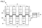
- FIG. 7 is a diagram schematically showing the configuration of the slitter 30 used in the fine wire processing step.
- the right side of FIG. 7 shows the configuration of the stacked body 20 that is slit by the slitter 30.
- the laminate 20 is formed by laminating the intermediate layer 3, the superconducting material layer 5, and the protective layer 7 in this order on the substrate 1.
- the slitter 30 includes a plurality of rotary blades 31 and a plurality of spacers 32.
- the slitter 30 has, for example, a total of seven rotary blades 31.
- Three rotary blades 31 having a width of about 4 mm are arranged on the rotary shaft on the upper side of the slitter 30.
- a spacer 32 is disposed between the rotary blades 31 adjacent in the rotation axis direction.
- Four rotating blades 31 having a width of about 4 mm are also arranged on the lower rotating shaft of the slitter 30.
- variety of the rotary blade 31 installed in an upper rotating shaft and a lower rotating shaft can be set arbitrarily.
- the laminated body 20 b slit by contact with the rotary blade 31 from the protective layer 7 side is adjusted by adjusting slit conditions such as the distance between adjacent rotary blades 31 and the overlapping height.
- the end portions in the width direction of the superconducting material layer 5 and the protective layer 7 protrude (the surface of the protective layer 7 has a concave shape).
- the laminated body 20b (4 mm width thin wire
- the edge portion is curved according to the direction (slit direction) in which the rotary blade 31 enters.
- the substrate 1 is curved toward the protective layer 7 at the edge portion of the thin wire (laminated body 20b) slit from the protective layer 7 side by the upper rotary blade 31.
- the protective layer 7 and the ceramic layer are curved toward the substrate 1 side.
- the width of the rotary blade 31 inserted from the substrate 1 side and the width of the rotary blade 31 inserted from the protective layer 7 side are the same, but the rotary blade 31 inserted from the protective layer 7 side.
- the rotary blade 31 corresponding to a predetermined line width (for example, 4 mm width) may be used, and the rotary blade 31 having a narrow width may be used by the rotary blade 31 inserted from the substrate 1 side.
- a stabilization layer forming step for forming the stabilization layer 9 around the thin-lined laminate 20 is performed.
- the stabilization layer 9 made of copper (Cu) or a copper alloy is publicly known so as to cover the outer periphery of the stacked body 20, that is, to cover almost the entire outermost surface of the stacked body 20. It is formed by a plating method.
- a method of forming the stabilization layer 9 there is a method of bonding a copper foil in addition to the plating method.
- superconducting wire 10 basically has the same structure as the superconducting wire shown in FIG. 1, but the back surface of substrate 1 constituting laminate 20 (upper portion on which intermediate layer 3 is formed).
- the back surface located on the opposite side of the front surface has a curved surface that is convex outward, and the back surface portion 26 of the stabilization layer 9 (the side opposite to the side on which the superconducting material layer 5 is formed as viewed from the substrate 1). 1 is different from the superconducting wire 10 shown in FIG. 1 in that the surface of the stabilization layer 9 located on the outer surface is curved outwardly. Further, in the superconducting wire 10 shown in FIG.
- both end surfaces (two side surfaces connecting the front surface portion 25 and the back surface portion 26) of the stabilization layer 9 are inclined with respect to each other.
- both end surfaces of the laminate 20 two side surfaces from which the substrate 1, the intermediate layer 3, the superconducting material layer 5, and the protective layer 7 are exposed) are also inclined in directions intersecting each other.
- the same effect as that of the superconducting wire 10 shown in FIG. 1 can be obtained by the superconducting wire 10 having such a structure.
- the widths of the front surface portion 25 and the back surface portion 26 are different, so that they are wound and laminated.
- a gap can be formed between the portion located on the inner peripheral side of the superconducting wire 10 and the portion located on the outer peripheral side. For this reason, compared with the case where the laminated
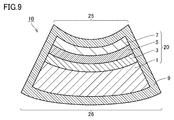
- the superconducting wire 10 shown in FIG. 9 basically has the same structure as the superconducting wire 10 shown in FIG. 8, but the curvature radius of the front surface portion 25 and the curvature radius of the back surface portion 26 are different. Specifically, in the superconducting wire 10 shown in FIG. 9, the curvature radius of the back surface portion 26 is larger than the curvature radius of the front surface portion 25. If it does in this way, when superconducting wire 10 is wound and laminated, it can prevent that surface part 25 of superconducting wire 10 of a lower layer side and back part 26 of superconducting wire 10 of the upper layer side stick. For this reason, it is possible to prevent the surface portion 25 from being damaged by other portions of the superconducting wire 10 laminated on the surface portion 25.
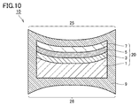
- superconducting wire 10 basically has the same structure as the superconducting wire shown in FIG. 1, except that back surface portion 26 of stabilizing layer 9 is recessed (curved surface) on the substrate 1 side. Part). Also in the superconducting wire 10 having such a structure, the same effect as that of the superconducting wire 10 shown in FIG. 1 can be obtained, and when the superconducting wire 10 is wound and laminated, the surface portion of the laminated superconducting wire 10 is obtained. 25 and the area of the superconducting wire 10 positioned on the front surface portion 25 (the back surface portion 26) can be reduced in area. For this reason, the probability that the surface part 25 will be damaged can be reduced. As a result, it is possible to suppress the occurrence of a problem that a defect occurs in the superconducting material layer 5 due to the scratch and the superconducting characteristics deteriorate.
- any method can be used.
- the electric field strength at the end of the laminate 20 in the width direction is set to other portions.
- a method can be used in which the thickness of the stabilization layer 9 at the end portion is relatively increased by increasing the electric field strength at.
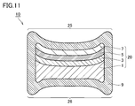
- the superconducting wire 10 shown in FIG. 11 basically has the same structure as that of the superconducting wire shown in FIG. 10, but the back surface of the substrate 1 constituting the laminate 20 (opposite to the surface on which the intermediate layer 3 is formed).
- the shape of the surface located on the side is different from the substrate 1 of the superconducting wire 10 shown in FIG. That is, the back surface of the substrate 1 of the superconducting wire 10 shown in FIG. 11 has a curved shape recessed toward the superconducting material layer 5 side.
- the shape of the back surface portion 26 of the stabilization layer 9 is also a curved concave shape along the shape of the back surface of the substrate 1.
- corner of the cross section of the substrate 1 of the superconducting wire 10 shown in FIG. 10 is an acute angle or a substantially right angled corner where two straight lines intersect, but the substrate 1 of the superconducting wire 10 shown in FIG.
- the corners in the cross section are curved. For this reason, the corners of the four corners of the outer periphery of the stabilization layer 9 in the cross section in the width direction of the superconducting wire 10 are also curved so as to follow the corners of the substrate 1.
- the laminated body 20 constituting the superconducting wire 10 shown in FIG. 11 can be obtained, for example, by laser slitting the wide laminated body 20. Further, the stabilization layer 9 shown in FIG. 11 can be formed by using any conventionally known method such as a plating method so as to cover the surface of the laminate 20.
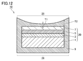
- superconducting wire 10 basically has the same structure as superconducting wire 10 shown in FIG. 1, but the shape of laminated body 20 is a laminated body 20 of superconducting wire 10 shown in FIG. The shape is different. That is, in the superconducting wire 10 shown in FIG. 12, the upper surfaces of the substrate 1, the intermediate layer 3, the superconducting material layer 5, and the protective layer 7 are substantially flat. Therefore, on the surface of the protective layer 7, the thickness T2 of the stabilizing layer 9 on the end portion of the protective layer 7 is thicker than the thickness T1 of the stabilizing layer 9 in the central portion of the protective layer 7.
- the thickness T2 of the stabilization layer 9 is sufficient. Since the thickness is increased, the influence of the pressure on the protective layer 7 and the superconducting material layer 5 can be reduced. Therefore, the risk that the superconducting material layer 5 is damaged by the stress from the outside can be reduced.
- a laminate 20 of the superconducting wire 10 shown in FIG. 12 prepares, for example, a substrate 1 having a rectangular cross-sectional shape that is the width of the laminate 20, and an intermediate layer 3 and a superconducting material layer on the main surface of the substrate 1. 5 and the protective layer 7 can be sequentially formed.
- the stabilization layer 9 shown in FIG. 12 can be formed by the same method as the stabilization layer 9 in the superconducting wire 10 shown in FIG. 10, for example.
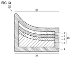
- FIG. 13 is a schematic sectional view showing a fifth embodiment of the superconducting wire 10 according to the present invention. A fifth embodiment of the superconducting wire according to the present invention will be described with reference to FIG.
- superconducting wire 10 basically has the same structure as superconducting wire 10 shown in FIG. 1, but the shape of surface portion 25 of laminate 20 and stabilizing layer 9 is shown in FIG. 1. It differs from the superconducting wire 10 shown. That is, in the superconducting wire 10 shown in FIG. 13, only one end portion of the upper surface of the substrate 1, the intermediate layer 3, the superconducting material layer 5 and the protective layer 7 constituting the laminate 20 is compared with the other end portion. Are configured to protrude. For this reason, the shape of the surface portion 25 of the stabilization layer 9 is also a concave shape and a curved surface shape while the one protruding end side of the laminate 20 protrudes.
- the shape of the surface portion 25 that has a concave curved surface as a result of one end projecting is also referred to as a concave shape in this specification.
- wound resulting from the contact with the other member in the surface part 25 etc. can be suppressed similarly to the superconducting wire 10 shown in FIG.
- the laminated body 20 of the superconducting wire 10 shown in FIG. 13 is a portion located at the end of the wide laminated body 20 (base material) to be thinned, for example, in the slitter 30 shown in FIG. (In other words, a portion where only one end is cut by the rotary blade 31) can be obtained as the laminate 20 shown in FIG.
- the stabilization layer 9 shown in FIG. 13 can be formed by a conventionally known method such as a plating method so as to surround the periphery of the stacked body 20.
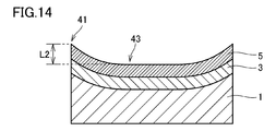
- FIG. 14 is a schematic diagram showing an intermediate stage of the manufacturing process of the superconducting wire according to the sixth embodiment of the present invention.
- intermediate layer 3 and superconducting material layer 5 are formed on the upper surface of substrate 1. Further, at this time, the surface of the superconducting material layer 5 is a curved concave portion that is recessed toward the substrate 1 side.
- the structure as shown in FIG. 14 can be obtained by any conventionally known method. For example, the substrate 1 having the cross-sectional shape as shown in FIG.
- the substrate 14 is prepared as the substrate 1, and the intermediate layer 3 and the superconducting material layer 5 are formed on the main surface (main surface recessed in a concave shape) of the substrate 1. May be.
- the intermediate layer 3 and the superconducting material layer 5 may be thinned using a slitter or the like shown in FIG.
- a cross-sectional structure (a laminated body of the substrate 1, the intermediate layer 3, and the superconducting material layer 5) may be obtained.
- the distance L2 in the thickness direction of the substrate 1 between the bottom 43 located at the center in the width direction of the superconducting material layer 5 and the top 41 located at the end in the width direction of the superconducting material layer 5 is, for example, 1 ⁇ m or more. It can be set to 100 ⁇ m or less.
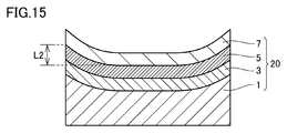
- the laminated body 20 shown in FIG. 15 can be obtained by forming the protective layer 7 on the superconducting material layer 5.
- FIG. 7 After forming the intermediate
- FIG. 15 a structure as shown in FIG. 15 may be obtained.
- the shape of the surface portion 25 of the stabilization layer 9 is as shown in FIG. It can be easily made into a curved shape (concave portion) that is recessed.
- the same effect as that of the superconducting wire 10 shown in FIG. 1 can be obtained by the superconducting wire 10 having the structure shown in FIG.
- the portion located at the end of the thinned laminate 20 is the slitting blade 31 of the slitter as described with respect to the method of manufacturing the superconducting wire 10 shown in FIG. 17 so that only one end in the width direction of the superconducting material layer 5 (and the protective layer 7) protrudes as shown in FIG.
- the surfaces of the superconducting material layer 5 and the protective layer 7 can be formed to have a concave curved surface.
- the distance L2 between the top 41 of the superconducting material layer 5 (the end on the protruding side of the superconducting material layer 5) and the bottom 43 (the end opposite to the protruding side of the superconducting material layer 5) is set. It can be 1 ⁇ m or more and 100 ⁇ m or less.
- a superconducting wire as shown in FIG. 13 may be configured by forming the stabilization layer 9 so as to cover the outer periphery of the laminate 20 using the laminate 20 having such a structure. Also in this case, the same effect as the superconducting wire shown in FIG. 1 can be obtained.
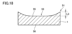
- FIG. 18 is a schematic cross-sectional view showing a substrate 1 for constituting a seventh embodiment of the superconducting wire according to the present invention.
- the substrate 1 shown in FIG. 18 has a concave curved surface shape (concave portion) in which the upper surface (main surface) is recessed.
- the back surface of the substrate 1 (the back surface opposite to the upper surface) has a flat shape.
- the distance L3 (the distance in the thickness direction of the substrate 1) between the top 51 and the bottom 53 of the upper surface can be 1 ⁇ m or more and 100 ⁇ m or less.
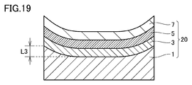
- the intermediate layer 3, the superconducting material layer 5, and the protective layer 7 are formed on the main surface of the substrate 1 as shown in FIG.
- the shapes of the upper surfaces of the intermediate layer 3, the superconducting material layer 5 and the protective layer 7 are concave along the shape of the main surface of the substrate 1.
- a laminate 20 composed of the substrate 1, the intermediate layer 3, the superconducting material layer 5, and the protective layer 7 can be obtained as shown in FIG.
- the stabilization layer 9 (see FIG. 20) is formed so as to surround the periphery of the stacked body 20. As a result, as shown in FIG.
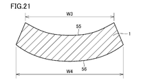
- FIG. 21 is a schematic cross-sectional view showing a substrate 1 for constituting an eighth embodiment of the superconducting wire according to the present invention.
- the width W4 of the other main surface (back surface 56) is wider than the width W3 of one main surface 55.
- one main surface 55 of the substrate 1 is a curved concave portion that is recessed toward the inside in the thickness direction of the substrate 1.
- the other main surface (back surface 56) is a curved convex portion protruding from the inside of the substrate 1 toward the outside.
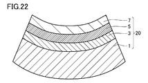
- the intermediate layer 3, the superconducting material layer 5, and the protective layer 7 are formed on one main surface 55 (the main surface 55 having a concave curved surface) of the substrate 1 as shown in FIG. As a result, the laminate 20 shown in FIG. 22 can be obtained.
- the process conditions at the time of thinning using the slitter 30 shown in FIG. 7 are adjusted. By doing so, you may obtain the laminated body 20 of a cross-sectional shape as shown in FIG.
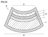
- the stabilization layer 9 is formed around the laminate 20 as shown in FIG.
- the back surface portion 26 of the stabilization layer 9 (the surface of the stabilization layer 9 at a position facing the back surface 56 of the substrate 1) is a curved surface portion (convex shape portion) having a convex shape protruding outward from the substrate 1. It has become.
- the width of the back surface portion 26 is wider than the width of the front surface portion 25 of the stabilization layer 9 as in the superconducting wire 10 shown in FIG. Can be reduced and the probability of occurrence of a problem such that contact is made between the portions of the superconducting wire 10 that are stacked and scratches occur in the surface portion 25 can be reduced.
- a modification of the substrate 1 shown in FIG. 21 will be described with reference to FIG.
- the substrate 1 shown in FIG. 24 basically has the same structure as the substrate 1 shown in FIG. 21, but the curvature radius of the back surface 56 is larger than the curvature radius of the main surface 55 of the substrate 1.
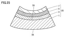
- a laminated body 20 can be obtained by forming the intermediate layer 3, the superconducting material layer 5, and the protective layer 7 on the main surface 55 of the substrate 1 thus configured as shown in FIG.
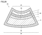
- the superconducting wire 10 as shown in FIG. 26 can be obtained by covering the outer periphery of the laminate 20 with the stabilization layer 9.
- the shapes of the front surface portion 25 and the back surface portion 26 of the stabilization layer 9 are in accordance with the shapes of the main surface 55 and the back surface 56 of the substrate 1, respectively.
- the curvature radius of the back surface portion 26 is larger than the curvature radius of the front surface portion 25 of the stabilization layer 9.
- the superconducting wire 10 shown in FIG. 26 can obtain the same effect as the superconducting wire shown in FIG.
- the superconducting wire 10 shown in FIG. 26 prepares the substrate 1 having the cross-sectional shape as shown in FIG. 24 from the beginning, and forms the intermediate layer 3, the superconducting material layer 5, the protective layer 7 and the like on the substrate 1.
- the stabilization layer 9 may be further formed.
- the intermediate layer 3, the superconducting material layer 5, the protective layer are formed on the main surface of the substrate 1 having a rectangular cross-sectional shape.
- the laminate 20 having a cross-sectional shape as shown in FIG. 25 may be obtained by adjusting processing conditions when thinning using the slitter 30 shown in FIG.
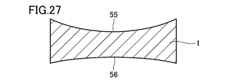
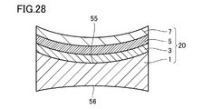
- FIG. 27 shows a substrate 1 constituting a ninth embodiment of the superconducting wire according to the present invention.
- the main surface 55 and the back surface 56 each have a concave curved shape that is recessed toward the inside of the substrate 1.
- the intermediate layer 3 On the main surface 55 of the substrate 1, the intermediate layer 3, the superconducting material layer 5, and the protective layer 7 are formed as shown in FIG.
- a laminate 20 as shown in FIG. 28 is obtained.
- the stabilization layer 9 is formed as shown in FIG. 29 so that the outer periphery of this laminated body 20 may be covered.
- FIG. 29 shows a result, as shown in FIG.
- the superconducting wire 10 shown in FIG. 29 it is possible to obtain the superconducting wire 10 in which the surface portion 25 and the back surface portion 26 of the stabilization layer have curved shapes that are recessed toward the substrate 1, respectively. Also by the superconducting wire 10 shown in FIG. 29, the same effect as the superconducting wire shown in FIG. 10 can be obtained.
- the shape of the back surface 56 of the substrate 1 of the laminate 20 and the upper surface of the protective layer 7 is a curved shape recessed toward the superconducting material layer 5 side. Therefore, by forming the stabilization layer 9 along the surface of the stacked body 20, it is possible to easily form the concave-shaped (curved surface) surface portion 25 and the back surface portion 26. And the effect similar to the superconducting wire 10 shown in FIG. 10 can be acquired also by the superconducting wire 10 shown in FIG.
- the present invention is advantageously applied particularly to a superconducting wire having a superconducting material layer formed on the surface of a substrate.
Landscapes
- Chemical & Material Sciences (AREA)
- Organic Chemistry (AREA)
- Engineering & Computer Science (AREA)
- Inorganic Chemistry (AREA)
- Power Engineering (AREA)
- Manufacturing & Machinery (AREA)
- Ceramic Engineering (AREA)
- Life Sciences & Earth Sciences (AREA)
- Geology (AREA)
- Superconductors And Manufacturing Methods Therefor (AREA)
- Inorganic Compounds Of Heavy Metals (AREA)
Abstract
Description
最初に本発明の実施態様を列記して説明する。
以下、本発明の実施の形態について図に基づいて説明する。なお、以下の図面において、同一または相当する部分には同一の参照番号を付し、その説明は繰り返さない。
(超電導線材の構成)
図1は、本発明の実施の形態1に係る超電導線材の構成を示す断面模式図である。図1は、実施の形態1に係る超電導線材10の延在する方向に交差する方向に切断した断面を示している。このため、紙面に交差する方向が超電導線材の長手方向であり、超電導材料層5の超電導電流は紙面に交差する方向に沿って流れるものとする。また、図1および以降の断面模式図においては、図を見やすくするために矩形状の断面における上下方向(以下、「厚み方向」とも称する)と左右方向(以下、「幅方向」とも称する)との長さの差を小さくしているが、実際は当該断面の厚み方向の長さは幅方向の長さに比べて十分に小さい。
図2~図7を参照して、図1に示した超電導線材10の製造方法を説明する。以下では、30mm幅に作製された積層体20から4mm幅に細線加工された積層体20を用いて超電導線材10を製造する方法を例に挙げ、本実施の形態を具体的に説明する。
図8を参照して、本発明による超電導線材の実施の形態2を説明する。
図10を参照して、本発明による超電導線材の実施の形態3を説明する。
図12を参照して、本発明による超電導線材の実施の形態4を説明する。図12を参照して、超電導線材10は、基本的には図1に示した超電導線材10と同様の構造を備えるが、積層体20の形状が図1に示した超電導線材10の積層体20の形状と異なっている。すなわち、図12に示した超電導線材10においては、基板1、中間層3、超電導材料層5および保護層7の上部表面がほぼ平坦な形状となっている。そのため、保護層7の表面上において保護層7の中央部における安定化層9の厚みT1より、保護層7の端部上における安定化層9の厚みT2の方が厚くなっている。このため、安定化層9の図12における端部側(安定化層9の凹形状となっている上部表面の端部)に応力が加わった場合においても、安定化層9の厚みT2が十分厚くなっているため、保護層7および超電導材料層5に当該圧力が及ぼす影響を軽減できる。したがって、超電導材料層5が外部からの当該応力により破損するといった危険性を低減できる。
図13は、本発明による超電導線材10の実施の形態5を示す断面模式図である。図13を参照して、本発明による超電導線材の実施の形態5を説明する。
図14は、本発明による超電導線材の実施の形態6の製造工程の途中段階を示す模式図である。図14を参照して、本発明による超電導線材の実施の形態6の製造方法においては、基板1の上部表面上に中間層3および超電導材料層5が形成される。また、このとき、超電導材料層5の表面が基板1側に凹んだ曲面状の凹部となっている。図14に示したような構造は、従来周知の任意の方法により得ることができる。たとえば、基板1として図14に示したような断面形状の基板1を準備し、当該基板1の主面(凹形状に凹んでいる主面)上に中間層3および超電導材料層5を形成してもよい。あるいは、断面形状が矩形状の基板1の主面上に中間層3、超電導材料層5を形成した後、図7に示したスリッターなどを用いて細線化することにより、図14に示すような断面形状の構造(基板1、中間層3、超電導材料層5の積層体)を得てもよい。
図18は、本発明による超電導線材の実施の形態7を構成するための基板1を示す断面模式図である。図18に示す基板1は、その上部表面(主面)が窪んだ凹形状の曲面状(凹部)となっている。なお、基板1の裏面(上部表面と反対側意の裏面)は平坦な形状である。また、当該上部表面の頂部51と底部53との間の距離L3(基板1の厚み方向における距離)は1μm以上100μm以下とすることができる。
図21は、本発明による超電導線材の実施の形態8を構成するための基板1を示す断面模式図である。図21に示した基板1は、一方の主面55の幅W3よりも他方の主面(裏面56)の幅W4の方が広くなっている。また、基板1の一方の主面55は基板1の厚み方向の内側に向けて窪んだ曲面状の凹部となっている。また、他方の主面(裏面56)は、基板1の内部から外側に向かって突出する曲面状の凸部となっている。
図27は、本発明による超電導線材の実施の形態9を構成する基板1を示している。図27に示した基板1においては、主面55および裏面56がそれぞれ基板1の内側に向けて窪んだ凹形状の曲面状となっている。この基板1の主面55上に、図28に示すように中間層3、超電導材料層5および保護層7を形成する。この結果、図28に示すような積層体20を得る。そして、この積層体20の外周を覆うように、図29に示すように安定化層9を形成する。この結果、図29に示すように安定化層の表面部分25と裏面部分26とがそれぞれ基板1側に窪んだ曲面状の形状となっている超電導線材10を得ることができる。図29に示した超電導線材10によっても、図10に示した超電導線材と同様の効果を得ることができる。また、図29に示した超電導線材10においては、積層体20の基板1の裏面56および保護層7の上部表面の形状が超電導材料層5側に窪んだ曲面状となっている。そのため、安定化層9を積層体20の表面に沿って形成することで、容易に窪んだ凹形状(曲面状)の表面部分25および裏面部分26を形成することができる。そして、図29に示した超電導線材10によっても、図10に示した超電導線材10と同様の効果を得ることができる。
Claims (13)
- 主面を有する基板と、前記主面上に形成された超電導材料層とを含む積層体と、
少なくとも前記超電導材料層上に配置された被覆層とを備え、
前記被覆層において、前記超電導材料層上に位置する表面部分は凹形状になっている、超電導線材。 - 前記基板の幅方向での断面において、前記表面部分の前記凹形状になっている領域の頂部と底部との間の、前記基板の厚み方向における距離は、1μm以上100μm以下である、請求項1に記載の超電導線材。
- 前記基板の幅方向での断面において、前記表面部分の幅は、前記超電導線材において前記表面部分と反対側に位置する領域の幅より狭い、請求項1または請求項2に記載の超電導線材。
- 前記超電導線材において前記表面部分と反対側に位置する裏面部分の形状は平面状および凹形状のいずれか一方である、請求項1~請求項3のいずれか1項に記載の超電導線材。
- 前記超電導線材において前記表面部分と反対側に位置する裏面部分の形状は凸状の曲面状であり、
前記表面部分の形状は凹状の曲面状であり、
前記基板の幅方向での断面において、前記裏面部分の曲率半径は前記表面部分の曲率半径より大きい、請求項1~請求項3のいずれか1項に記載の超電導線材。 - 前記基板の幅方向での断面において、前記超電導材料層の中央部上における前記安定化層の厚みより、前記超電導材料層の端部上における前記被覆層の厚みの方が厚い、請求項1~請求項5のいずれか1項に記載の超電導線材。
- 主面を有する基板と、
前記主面上に形成された超電導材料層とを備え、
前記超電導材料層の表面は凹形状になっている、超電導線材。 - 前記基板の幅方向での断面において、前記超電導材料層の表面の凹形状になっている領域の頂部と底部との間の、前記基板の厚み方向における距離は、1μm以上100μm以下である、請求項7に記載の超電導線材。
- 主面を有する基板と、
前記主面上に形成された超電導材料層とを備え、
前記基板の前記主面は凹形状になっている、超電導線材。 - 前記基板の幅方向での断面において、前記基板の前記主面の凹形状になっている領域の頂部と底部との間の、前記基板の厚み方向における距離は、1μm以上100μm以下である、請求項9に記載の超電導線材。
- 前記基板の幅方向での断面において、前記主面の幅は、前記基板において前記主面と反対側に位置する領域の幅より狭い、請求項9または請求項10に記載の超電導線材。
- 前記基板において前記主面と反対側に位置する裏面の形状は平面状および凹形状のいずれか一方である、請求項9~請求項11のいずれか1項に記載の超電導線材。
- 前記基板において前記主面と反対側に位置する裏面の形状は凸状の曲面状であり、
前記主面の形状は凹状の曲面状であり、
前記基板の幅方向での断面において、前記裏面の曲率半径は前記主面の曲率半径より大きい、請求項9~請求項11のいずれか1項に記載の超電導線材。
Priority Applications (5)
| Application Number | Priority Date | Filing Date | Title |
|---|---|---|---|
| US15/320,935 US10460854B2 (en) | 2014-07-31 | 2015-03-16 | Superconducting wire |
| DE112015003516.8T DE112015003516T5 (de) | 2014-07-31 | 2015-03-16 | Supratleitender Draht |
| CN201580041318.7A CN106575551B (zh) | 2014-07-31 | 2015-03-16 | 超导线材 |
| KR1020177005464A KR102286710B1 (ko) | 2014-07-31 | 2015-03-16 | 초전도 선재 |
| US16/574,907 US11264151B2 (en) | 2014-07-31 | 2019-09-18 | Superconducting wire |
Applications Claiming Priority (2)
| Application Number | Priority Date | Filing Date | Title |
|---|---|---|---|
| JP2014-156649 | 2014-07-31 | ||
| JP2014156649A JP6225851B2 (ja) | 2014-07-31 | 2014-07-31 | 超電導線材 |
Related Child Applications (2)
| Application Number | Title | Priority Date | Filing Date |
|---|---|---|---|
| US15/320,935 A-371-Of-International US10460854B2 (en) | 2014-07-31 | 2015-03-16 | Superconducting wire |
| US16/574,907 Division US11264151B2 (en) | 2014-07-31 | 2019-09-18 | Superconducting wire |
Publications (1)
| Publication Number | Publication Date |
|---|---|
| WO2016017203A1 true WO2016017203A1 (ja) | 2016-02-04 |
Family
ID=55217108
Family Applications (1)
| Application Number | Title | Priority Date | Filing Date |
|---|---|---|---|
| PCT/JP2015/057641 Ceased WO2016017203A1 (ja) | 2014-07-31 | 2015-03-16 | 超電導線材 |
Country Status (6)
| Country | Link |
|---|---|
| US (2) | US10460854B2 (ja) |
| JP (1) | JP6225851B2 (ja) |
| KR (1) | KR102286710B1 (ja) |
| CN (1) | CN106575551B (ja) |
| DE (1) | DE112015003516T5 (ja) |
| WO (1) | WO2016017203A1 (ja) |
Cited By (1)
| Publication number | Priority date | Publication date | Assignee | Title |
|---|---|---|---|---|
| CN110392915A (zh) * | 2017-03-07 | 2019-10-29 | 住友电气工业株式会社 | 超导线材、超导线圈和超导电缆导体 |
Families Citing this family (9)
| Publication number | Priority date | Publication date | Assignee | Title |
|---|---|---|---|---|
| JP6078522B2 (ja) * | 2014-12-16 | 2017-02-08 | 株式会社フジクラ | 超電導線材及びこれを使用した超電導コイル |
| WO2017081762A1 (ja) | 2015-11-11 | 2017-05-18 | 住友電気工業株式会社 | 超電導線材 |
| DE112017007057T5 (de) * | 2017-02-14 | 2019-10-24 | Sumitomo Electric Industries, Ltd. | Supraleitender draht und supraleitende spule |
| CN108257729B (zh) * | 2017-12-13 | 2024-07-05 | 无锡友方电工股份有限公司 | 磁共振磁体mri月牙形超导基体、超导线及制造方法 |
| US11101215B2 (en) * | 2018-09-19 | 2021-08-24 | PsiQuantum Corp. | Tapered connectors for superconductor circuits |
| CA3173407A1 (en) | 2020-03-26 | 2021-09-30 | Brian LABOMBARD | Passive quench protection techniques for non-insulated superconducting magnets |
| EP4128289B1 (en) * | 2020-03-26 | 2025-09-03 | Massachusetts Institute Of Technology | Conductor and coolant schemes for spiral-grooved, stacked plates, non-insulated superconducting magnets |
| KR102859569B1 (ko) | 2020-05-20 | 2025-09-15 | 메사추세츠 인스티튜트 오브 테크놀로지 | 하이 필드 자석들에서 힘들을 분배하는 기술들 및 관련 시스템들 및 방법들 |
| CN115171974B (zh) * | 2022-07-22 | 2023-08-01 | 上海超导科技股份有限公司 | 铜合金加强的超导带材、加强方法、超导线圈及超导线缆 |
Citations (2)
| Publication number | Priority date | Publication date | Assignee | Title |
|---|---|---|---|---|
| JP2004031128A (ja) * | 2002-06-26 | 2004-01-29 | Sumitomo Electric Ind Ltd | 超電導薄膜線材およびその製造方法、ならびに超電導ケーブル導体 |
| JP2013246881A (ja) * | 2012-05-23 | 2013-12-09 | Chubu Electric Power Co Inc | 超電導線材の絶縁被覆構造 |
Family Cites Families (14)
| Publication number | Priority date | Publication date | Assignee | Title |
|---|---|---|---|---|
| CN1200435C (zh) | 2001-08-08 | 2005-05-04 | 北京英纳超导技术有限公司 | 高温超导线材的制备方法 |
| US6745059B2 (en) | 2001-11-28 | 2004-06-01 | American Superconductor Corporation | Superconductor cables and magnetic devices |
| JP2012014883A (ja) | 2010-06-30 | 2012-01-19 | Railway Technical Research Institute | 高温超電導線材およびそれを用いた高温超電導コイル |
| JP5757718B2 (ja) | 2010-10-27 | 2015-07-29 | 公益財団法人国際超電導産業技術研究センター | 酸化物超電導線材の製造方法 |
| JP5684601B2 (ja) | 2011-01-25 | 2015-03-18 | 株式会社フジクラ | 酸化物超電導線材およびその製造方法 |
| JP6040515B2 (ja) * | 2011-03-17 | 2016-12-07 | 富士電機株式会社 | 超電導コイルの製造方法 |
| JP2013012406A (ja) | 2011-06-29 | 2013-01-17 | Sumitomo Electric Ind Ltd | 酸化物超電導薄膜線材の製造方法 |
| KR101617554B1 (ko) | 2011-08-02 | 2016-05-02 | 후루카와 덴키 고교 가부시키가이샤 | 초전도 도체의 제조방법, 초전도 도체 및 초전도 도체용 기판 |
| RU2570047C1 (ru) * | 2011-11-21 | 2015-12-10 | Фуджикура Лтд. | Оксидный сверхпроводящий провод и способ изготовления оксидного сверхпроводящего провода |
| EP2728590B9 (en) | 2012-04-16 | 2018-09-05 | Furukawa Electric Co., Ltd. | Substrate for superconducting film, superconducting wire, and superconducting wire fabrication method |
| CN103813690A (zh) * | 2012-11-08 | 2014-05-21 | 鸿富锦精密工业(深圳)有限公司 | 导风罩 |
| US10186651B2 (en) * | 2014-05-08 | 2019-01-22 | Fujikura Ltd. | Oxide superconducting wire and method of manufacturing oxide superconducting wire |
| JP6256244B2 (ja) * | 2014-07-31 | 2018-01-10 | 住友電気工業株式会社 | 超電導線材 |
| WO2017081762A1 (ja) * | 2015-11-11 | 2017-05-18 | 住友電気工業株式会社 | 超電導線材 |
-
2014
- 2014-07-31 JP JP2014156649A patent/JP6225851B2/ja active Active
-
2015
- 2015-03-16 CN CN201580041318.7A patent/CN106575551B/zh active Active
- 2015-03-16 KR KR1020177005464A patent/KR102286710B1/ko active Active
- 2015-03-16 DE DE112015003516.8T patent/DE112015003516T5/de not_active Withdrawn
- 2015-03-16 WO PCT/JP2015/057641 patent/WO2016017203A1/ja not_active Ceased
- 2015-03-16 US US15/320,935 patent/US10460854B2/en active Active
-
2019
- 2019-09-18 US US16/574,907 patent/US11264151B2/en active Active
Patent Citations (2)
| Publication number | Priority date | Publication date | Assignee | Title |
|---|---|---|---|---|
| JP2004031128A (ja) * | 2002-06-26 | 2004-01-29 | Sumitomo Electric Ind Ltd | 超電導薄膜線材およびその製造方法、ならびに超電導ケーブル導体 |
| JP2013246881A (ja) * | 2012-05-23 | 2013-12-09 | Chubu Electric Power Co Inc | 超電導線材の絶縁被覆構造 |
Cited By (1)
| Publication number | Priority date | Publication date | Assignee | Title |
|---|---|---|---|---|
| CN110392915A (zh) * | 2017-03-07 | 2019-10-29 | 住友电气工业株式会社 | 超导线材、超导线圈和超导电缆导体 |
Also Published As
| Publication number | Publication date |
|---|---|
| US10460854B2 (en) | 2019-10-29 |
| CN106575551B (zh) | 2019-03-15 |
| JP2016033885A (ja) | 2016-03-10 |
| JP6225851B2 (ja) | 2017-11-08 |
| US20200111589A1 (en) | 2020-04-09 |
| KR102286710B1 (ko) | 2021-08-05 |
| CN106575551A (zh) | 2017-04-19 |
| US11264151B2 (en) | 2022-03-01 |
| KR20170038029A (ko) | 2017-04-05 |
| DE112015003516T5 (de) | 2017-04-27 |
| US20170133127A1 (en) | 2017-05-11 |
Similar Documents
| Publication | Publication Date | Title |
|---|---|---|
| JP6225851B2 (ja) | 超電導線材 | |
| JP5402518B2 (ja) | 酸化物超電導コイル、酸化物超電導コイル体および回転機 | |
| KR102562414B1 (ko) | 초전도 선재 및 초전도 코일 | |
| JP6256244B2 (ja) | 超電導線材 | |
| JP2016530673A (ja) | ラミネート構造を持つ超電導線材およびその製造方法 | |
| WO2016017204A1 (ja) | 超電導線材 | |
| JP6465217B2 (ja) | 超電導線材 | |
| JP5727278B2 (ja) | 酸化物超電導薄膜線材の製造方法 | |
| JP2016033883A (ja) | 超電導線材 | |
| JP5393267B2 (ja) | 超電導線材の製造方法 | |
| JP6729303B2 (ja) | 超電導線材及び超電導コイル | |
| KR102302847B1 (ko) | 초전도 선재 | |
| JP2017152210A (ja) | 酸化物超電導線材及びその製造方法 | |
| KR20190092436A (ko) | 초전도 선재 및 그 제조 방법 | |
| WO2016185751A1 (ja) | 超電導線材 | |
| JP2010282892A (ja) | 超電導線材 |
Legal Events
| Date | Code | Title | Description |
|---|---|---|---|
| 121 | Ep: the epo has been informed by wipo that ep was designated in this application |
Ref document number: 15826939 Country of ref document: EP Kind code of ref document: A1 |
|
| WWE | Wipo information: entry into national phase |
Ref document number: 15320935 Country of ref document: US |
|
| WWE | Wipo information: entry into national phase |
Ref document number: 112015003516 Country of ref document: DE |
|
| ENP | Entry into the national phase |
Ref document number: 20177005464 Country of ref document: KR Kind code of ref document: A |
|
| 122 | Ep: pct application non-entry in european phase |
Ref document number: 15826939 Country of ref document: EP Kind code of ref document: A1 |