WO2016006539A1 - 荷電粒子線装置および収差補正器 - Google Patents
荷電粒子線装置および収差補正器 Download PDFInfo
- Publication number
- WO2016006539A1 WO2016006539A1 PCT/JP2015/069220 JP2015069220W WO2016006539A1 WO 2016006539 A1 WO2016006539 A1 WO 2016006539A1 JP 2015069220 W JP2015069220 W JP 2015069220W WO 2016006539 A1 WO2016006539 A1 WO 2016006539A1
- Authority
- WO
- WIPO (PCT)
- Prior art keywords
- multipole
- magnetic field
- charged particle
- particle beam
- electrostatic
- Prior art date
- Legal status (The legal status is an assumption and is not a legal conclusion. Google has not performed a legal analysis and makes no representation as to the accuracy of the status listed.)
- Ceased
Links
Images





Classifications
-
- H—ELECTRICITY
- H01—ELECTRIC ELEMENTS
- H01J—ELECTRIC DISCHARGE TUBES OR DISCHARGE LAMPS
- H01J37/00—Discharge tubes with provision for introducing objects or material to be exposed to the discharge, e.g. for the purpose of examination or processing thereof
- H01J37/02—Details
- H01J37/04—Arrangements of electrodes and associated parts for generating or controlling the discharge, e.g. electron-optical arrangement or ion-optical arrangement
- H01J37/153—Electron-optical or ion-optical arrangements for the correction of image defects, e.g. stigmators
-
- H—ELECTRICITY
- H01—ELECTRIC ELEMENTS
- H01J—ELECTRIC DISCHARGE TUBES OR DISCHARGE LAMPS
- H01J2237/00—Discharge tubes exposing object to beam, e.g. for analysis treatment, etching, imaging
- H01J2237/153—Correcting image defects, e.g. stigmators
- H01J2237/1534—Aberrations
Definitions
- the present invention relates to a charged particle beam apparatus.
- the invention also relates to an aberration corrector used for charged particle beams.
- the difference from the high-acceleration TEM and STEM is that the energy of the electron beam targeted by the SEM is low, so that chromatic aberration becomes the main factor limiting the resolution to the same level or higher than spherical aberration.
- SEM, low-acceleration TEM / STEM (especially with an energy of 30 VkeV or less) is required for a color / spherical aberration corrector having a different configuration from the hexapole spherical aberration corrector widely used in high-acceleration TEM and STEM.
- Patent Document 1 A chromatic (spherical) aberration corrector has been proposed (Patent Document 1).
- These aberration correctors are basically composed of two or more stages of quadrupole-octupole lenses.
- at least two of the multistage multipoles constituting this are electromagnetic composite quadrupoles that generate a quadrupole field of a magnetic field and an electrostatic field at the same location in order to correct chromatic aberration. Become.
- each multipole of the quadrupole-octupole chromatic / spherical aberration corrector is not limited to the above-mentioned electromagnetic composite quadrupole, but actually, other multipoles are often composed of 12 poles.
- This chromatic / spherical aberration corrector 6 is composed of four-stage multipole elements 20, 21, and 22, 23, 24, and 25. As described above, the inner two stages are magnetic quadrupole elements 21, 23. And the electrostatic quadrupoles 22 and 24 are generated by the same multipole.
- the multipole elements 20 and 25 before and after the main purpose are to guide electrons to the orbit suitable for chromatic aberration correction in the electromagnetic composite quadrupoles 21-22 and 23-24.
- the electromagnetic composite quadrupoles 21-22 and 23-24 are used. J. Zach et al. Used electrostatic quadrupoles for the front and rear multipoles 20 and 25, but these may be magnetic quadrupoles.
- the electrons are incident in parallel from the left side of the aberration corrector as shown in FIG. 8, and are emitted in parallel from the end of the corrector following the trajectories 100x and 100y.
- the distance from the central axis of the electron beam at the time of entering and exiting the corrector is also set to be equal. And it is devised so that it can be used for telescopic without affecting the optical system outside the corrector by turning on / off the aberration corrector.
- the electron beam incident from the left side is branched into the x orbit 100x and the y orbit 100y by the first stage quadrupole 20, and the second stage electromagnetic composite quadrupole 21-22 is connected.
- X orbit 100x passes off the axis.
- the y trajectory 100y is adjusted so as to pass almost the center of the composite quadrupole. Assuming that the field distribution is a rectangular field approximation, the motion of electrons inside the second-stage electromagnetic composite quadrupole is described by the following equation of motion:
- L ⁇ is the pole length
- ⁇ is a parameter representing the quadrupole field strength as shown in the following equation (2).
- ⁇ E and ⁇ M are parameters representing the electrostatic quadrupole and magnetic quadrupole strengths, respectively, as developed in Equation (2).
- Equation (3) The magnetic potential and electrostatic potential distribution of the quadrupole field with the coefficients ⁇ 2 and ⁇ 2 of the three items in Equation (2) are given by Equation (3) below.
- Equation (2) e and m are the charge and mass of the electrons, and ⁇ 0 is the energy of the electrons when passing through the aberration corrector. Taking into account the distribution of electron energy, Eq. (2) is transformed into Eq. (4) below for electrons with ⁇ 0 + ⁇ energy.
- ⁇ is the change in quadrupole strength with respect to the change (distribution) of electron energy.
- the two formulas (2) and (5) are obtained by using the electromagnetic composite quadrupole, while maintaining a constant value for the total strength (ie, formula (2)), while the variance (ie, formula (5) )) Can be adjusted to positive or negative.
- the second quadrupole 21-22 which is an electromagnetic composite, can create a convex lens with negative dispersion in the x direction and give negative chromatic aberration to electrons in the x orbit 100x.
- the dependence of the electrostatic quadrupole and the magnetic quadrupole on the electron energy ⁇ 0 is different, so a convex lens is formed with the magnetic quadrupole and a concave lens is formed with the electrostatic quadrupole in the x direction. It can be said that a negative chromatic aberration was produced by forming a convex lens having negative dispersion as a part.
- the y-orbit 100y is adjusted so that it passes through the center of the second quadrupole 21-22, so that 100y passes through it without being affected by the quadrupole including aberrations. To do.
- the x orbit 100x is at the center of the quadrupole and the y100 orbit 100y is off the axis so that it is antisymmetric with the second and quadrupole 21-22.
- the x orbit 100x is at the center of the quadrupole and the y100 orbit 100y is off the axis so that it is antisymmetric with the second and quadrupole 21-22.
- Electrons that have followed the x and y orbits branched up to this point are integrated stigmatically again by the fourth quadrupole 25 and exit from the aberration corrector 6.
- the above-described antisymmetric quadrupole aberration corrector can provide an equal amount of chromatic aberration in the x and y ⁇ ⁇ ⁇ directions, and thus rotationally symmetric and positively and negatively adjustable chromatic aberration, which is optically downstream from the aberration corrector 6.
- an antisymmetric quadrupole aberration corrector can correct chromatic aberration and third-order aperture aberration.
- the four-stage quadrupoles maintain the symmetry with respect to the x orbit and the y orbit, so that higher-order aberrations of the fourth or higher order are offset inside the aberration corrector by symmetry.
- the first stage 20, the fourth stage 25, the second stage 21-22, and the third stage 23-24 are arranged symmetrically on the center plane 15 in the aberration corrector and are excited antisymmetrically at the same time. That is, it becomes an antisymmetric quadrupole.
- a multistage multipole aberration corrector including two or more electromagnetic composite quadrupoles is constructed, and the negative chromatic aberration generated by the electromagnetic composite quadrupoles
- Chromatic aberration correction is realized by offsetting positive chromatic aberration, which is a problem in charged particle optical systems such as SEM objective lenses.
- FIGS. 9A and 9B are structural examples of the complexity of the mechanical structure of the conventional chromatic / spherical aberration corrector as described above.
- the second and third multipoles must have a complex structure as shown in FIGS. 9A and 9B because they need to be electromagnetic composites. That is, as shown in FIGS. 9A and 9B, the multipole of the second-stage multipole forms an electrostatic quadrupole field in the vacuum portion near the central axis 14, so that the tip of the pole 210a is exposed in the vacuum. There must be. Also, sufficient electrical insulation must be maintained between the poles or between the poles and the support material 260.
- the pole 210a since the pole 210a is also a magnetic pole, it must have a coil 211a for exciting it.
- the exciting coil has a large surface area, which causes gas emission and generates heat when energized.
- the tip of the pole 210a is placed in a vacuum and the other end of 210a is provided with an exciting coil 211a so that the support 260 is placed on the atmosphere side. It is to be. Furthermore, it is necessary to maintain electrical insulation between the support material 260 and the pole 210a with an insulating sleeve 214a interposed therebetween. Of course, since vacuum sealing must also be performed at the same location, at the location of the electromagnetic composite pole 210a, double O-rings (cross section) are provided at both locations between the pole 210a and the insulation sleeve 214a, and between the insulation sleeve 214a and the support material 260.
- a circular ring-shaped sealing mechanical part is sandwiched.
- the arrangement accuracy of the tip of the multipole is maintained on the order of ⁇ m, and at the same time, a magnetically uniform connection is maintained over the entire multipole, and the electrical insulation and vacuum sealing as described above are performed. It can be said that it is very difficult to realize a structure that satisfies the functions.
- the multistage multipole color / spherical aberration corrector includes an electromagnetic composite quadrupole compared to the hexapole spherical aberration corrector for high acceleration TEM and STEM.
- the stability of the power source for driving this is one digit higher.
- a power source having a stability of 10 ⁇ 5 to 10 ⁇ 6 is required, whereas in the latter color / spherical aberration corrector, A power supply with a stability higher than -7 to 10 -8 is required.
- one object of the present invention is to simplify the above-mentioned complicated mechanical structure as much as possible, and to easily improve the mechanical arrangement accuracy of the tip of the multipole and the magnetic uniformity of the entire multipole.
- Another problem is to reduce the required power supply stability of the drive power supply required for the multistage multipole color / spherical aberration corrector equipped with the same type of electromagnetic composite multipole compared to the conventional one.
- one aspect of the present invention provides a charged particle beam apparatus that irradiates a charged particle beam to a sample and detects charged particles caused by the sample.
- first and second electrostatic multipoles provided between the first magnetic field type multipole element and the second magnetic field type multipole element.
- the electrostatic multipole is arranged symmetrically with respect to the central symmetry plane, and is excited in anti-symmetric manner, and the first plane on which the second magnetic field type multipole is provided and the first electrostatic type Unlike the second plane provided with the multipole, the third plane provided with the third magnetic field type multipole and the second electrostatic type. Different from the fourth plane pole is provided, installing the aberration correction unit, wherein the path for detecting the charged particles caused by the path for irradiating a charged particle beam or the sample, in the sample that.
- a charged particle beam apparatus that irradiates a sample with a charged particle beam and detects charged particles caused by the sample, the first and second magnetic field type multipoles, and the first
- a third magnetic field type multipole element provided between one magnetic field type multipole element and a second magnetic field type multipole element; the first to fourth magnetic field type multipole elements;
- the second electrostatic multipole and the second electrostatic multipole are arranged symmetrically with respect to the central symmetry plane and excited in anti-symmetric manner, respectively, and the magnetic field acting on the second magnetic multipole and the first electrostatic multipole
- the width of the electric field acting on the third multipole element is different, and the width of the magnetic field acting on the third magnetic multipole element and the electric field acting on the second electrostatic multipole element are different.
- the multipole element provided on a plane has four or more stages.
- a second electrostatic multipole element provided on a third plane below the second plane, and a second electrostatic multipole element provided on a fourth plane below the third plane is provided between the first magnetic field type multipole element and the second magnetic field type multipole element, and is excited antisymmetrically with respect to the central symmetry plane of the aberration corrector.
- the second magnetic field type element, and the aberration corrector includes a first electric field generated by the first electrostatic multipole element and the second electric field type element.
- An aberration correction unit characterized by forming a fourth field in which one of the magnetic fields acts alone, or a path for irradiating the charged particle beam to the sample, or charged particles resulting from the sample. Install in the path to be detected.
- a third magnetic field type multipole element and a third magnetic field type multipole element provided between the first magnetic field type multipole element and the second magnetic field type multipole element.
- a fourth magnetic field type multipole, and first and second electrostatic type multipoles provided between the first magnetic field type multipole and the second magnetic field type multipole,
- the first to fourth magnetic field type multipole elements and the first and second electrostatic type multipole elements are arranged symmetrically with respect to a central symmetry plane, and are excited antisymmetrically.
- the first plane provided with the magnetic field type multipole and the second plane provided with the first electrostatic type multipole are different from the third plane provided with the third magnetic type multipole and the first plane.
- the aberration corrector is different from the fourth plane provided with the second electrostatic multipole element.
- a third magnetic field type multipole element and a third magnetic field type multipole element provided between the first magnetic field type multipole element and the second magnetic field type multipole element.
- the fourth magnetic field type multipole element, the first to fourth magnetic field type multipole elements, and the first and second electrostatic multipole elements are arranged symmetrically with respect to the central symmetry plane, and A magnetic field that is excited antisymmetrically and has a different width between the magnetic field on which the second magnetic multipole acts and the electric field on which the first electrostatic multipole acts, and on which the third magnetic multipole acts And an electric field applied to the second electrostatic multipole are different from each other in an aberration corrector.
- FIG. 1 It is a figure which shows the general structural example of SEM provided with the aberration corrector of a multistage multipole. It is a figure which shows one pole structure of the antisymmetric multiple quadrupole color and spherical aberration corrector of the invention, and an electron trajectory for aberration correction. It is a figure which shows another pole structure of the antisymmetric multiple quadrupole color and spherical aberration corrector of the invention, and an electron trajectory for aberration correction. It is a graph which shows that more stable chromatic aberration correction can be realized by using the aberration corrector configuration of the present invention than by using the conventional configuration.
- FIG. 2 of the present invention shows the mechanical structural example (vertical cross section) of the antisymmetric multiple quadrupole color and spherical aberration corrector shown in FIG. 2 of the present invention. It is a figure which shows the mechanical structural example (horizontal cross section) of the antisymmetric multiple quadrupole color and spherical aberration corrector shown in FIG. 2 of the present invention. It is a figure which shows the structural example (vertical cross section) of an electrostatic quadrupole part among the mechanical structures illustrated to FIG. 6A of this invention.
- FIG. 6B It is a figure which shows the structural example (horizontal cross section) of an electrostatic quadrupole part among the mechanical structures illustrated to FIG. 6B of this invention. It is a figure which shows the pole structure of the conventional antisymmetric quadrupole color and spherical aberration corrector, and the electron trajectory for aberration correction. It is a figure which shows the example of a mechanical structure (vertical cross section) of the conventional antisymmetric quadrupole color and spherical aberration corrector. It is a figure which shows the mechanical structural example (horizontal cross section) of the conventional antisymmetric quadrupole color and spherical aberration corrector.
- the present invention relates to a charged particle optical device that requires high resolution, and more particularly to a device that uses low energy charged particles in which chromatic aberration is a major factor in limiting the resolution.
- a simple color / spherical aberration corrector is not specifically limited, the following is described with the use in a low acceleration scanning electron microscope (SEM) and a scanning transmission electron microscope (STEM) in mind.
- the basic solution presented by the present invention is to separate the electromagnetic composite multipole included in the conventional multistage multipole color / spherical aberration corrector into separate electrostatic multipoles and magnetic multipoles, and It is to provide a difference in position or width on the electron beam path.
- the complex electromagnetic multipole having a complicated structure as described above is eliminated, and a simple electrostatic multipole and magnetic multipole can be separately arranged inside and outside the vacuum.
- a specific configuration example of the multistage multipole color / spherical aberration corrector according to the present invention will be described later with reference to FIGS. 6A and 6B, FIGS. 7A and 7B.
- the charged particle beam apparatus is a charged particle beam apparatus that irradiates a sample with a charged particle beam and detects signals such as charged particles and electromagnetic waves generated from the sample according to the irradiation.
- a multistage multipole color / spherical aberration corrector for reducing the particle beam irradiation diameter to be smaller is provided.
- the multistage multipole color / spherical aberration corrector includes two magnetic field type multipoles that form at least a quadrupole field at both ends or positions close to both ends, and further between the magnetic field type multipole pairs.
- the structure basically includes a pair of two magnetic multipoles and two electrostatic multipoles that are different from the four magnetic multipoles.
- the four multipoles are referred to as first to fourth magnetic field type multipoles from the incident end to the exit end of the charged particle beam.
- the two electrostatic multipoles are also incident ends.
- the first and second electrostatic multipoles will be referred to in order from the side.
- the paired first and fourth magnetic multipoles, second and third magnetic multipoles, and first and second electrostatic multipoles are symmetrical with respect to the center plane of the aberration corrector. And has the function of forming a quadrupole field with antisymmetric strength.
- the second electrostatic multipole element and the first magnetic field type multipole element, or the third electrostatic multipole element and the second magnetic field type multipole element are arranged at the same location on the charged particle path.
- the first means according to the present application is to maintain the symmetry of the arrangement with respect to the center plane of the aberration corrector and the antisymmetry of the excitation while maintaining the second magnetic field type multipole element and the first electrostatic type multipole element. Therefore, the third magnetic multipole and the second electrostatic multipole are arranged at positions where they are not completely overlapped on the charged particle path. This is because the second magnetic multipole and the first electrostatic multipole (and the third magnetic multipole and second electrostatic multipole so as to maintain symmetry) are partially This includes cases where they are arranged with overlap.
- the second means according to the present application is to maintain the symmetry of the arrangement with respect to the center plane of the aberration corrector and the anti-symmetry of the excitation while maintaining the second magnetic multipole and the first electrostatic multipole. Therefore, there is a difference between the pole lengths of the third magnetic field type multipole element and the second electrostatic type multipole element (the action length of the multipole element along the charged particle path). It is to give a difference to the distribution of the multipole field of both poles.
- another means according to the present application combines the above first and second means, and the second magnetic multipole and the first electrostatic multipole, and thus the third magnetic multipole and the second magnetic multipole. It is to change both the position and the pole length of the electrostatic multipole.
- an electromagnetic composite multipole having a complicated structure can be eliminated and replaced with a set of an electrostatic multipole and a magnetic multipole. While the electrostatic multipole body is set in a vacuum, if a vacuum container made of non-magnetic material is used, the magnetic field type multipole can be placed outside the vacuum together with the coils required for excitation, which is necessary for the electromagnetic composite type multipole. It is possible to greatly simplify the complicated electrical insulation or complicated structure for vacuum sealing. Thereby, it is possible to improve the mechanical accuracy in each of the electrostatic multipole element and the magnetic field multipole element.
- the present invention there is a problem of alleviating the stability and high accuracy required for the power source for driving the corrector.
- the specific values vary depending on the actual configuration of the multistage multipole aberration corrector, the configuration of the charged particle beam apparatus using the multistage multipole aberration corrector, the type of charged particle to be corrected, the energy, etc., but the electromagnetic complex quadrupole is corrected for chromatic aberration.
- the magnetic quadrupole convex lens and the electrostatic quadrupole concave lens generated by the electromagnetic composite multipole are used.
- a negative chromatic aberration is realized as a lens action that cancels a considerable part and remains.
- the power supply accuracy required for chromatic aberration correction using the difference between these positions and widths as adjustment parameters It was found that it can be reduced by 40-50% depending on the conditions.
- FIG. 1 shows a general configuration of an SEM equipped with a multistage multipole aberration corrector as in the present invention.
- the SEM barrel part 1 has an electron gun 3 including an electron source, an electron lens 3 that converges, and an objective lens 11 for forming a micro electron probe by reducing and projecting the electron on the sample 12, and the electron to the objective lens.
- an electron gun 3 including an electron source, an electron lens 3 that converges, and an objective lens 11 for forming a micro electron probe by reducing and projecting the electron on the sample 12, and the electron to the objective lens.
- the converging lens 4 may be used in more stages for the purpose of further increasing the reduction ratio.
- a scanning coil 10 for scanning the electron probe formed as described above on the sample surface is provided, and a detector 9 for detecting secondary electrons and reflected electrons emitted from the sample surface by the electron probe is provided.
- the detector 9 in FIG. 1 illustrates a secondary electron detector.
- the sample 12 is placed and observed in the sample chamber 2 on a sample holder 13 that can be horizontally moved and tilted.
- the intensity of secondary electrons and the like obtained by scanning the sample surface with the electron probe is sent to the control console 50, and is again two-dimensionally mapped according to the raster scan, that is, can be observed and recorded as an SEM image.
- the control console 50 here includes a control unit and an input / output unit.
- the multistage multipole aberration corrector 6 is placed upstream of the objective lens 11 in order to mainly correct chromatic aberration and spherical aberration of the objective lens 11. Further, in order to suppress the occurrence of coupling aberration between the aberration corrector 6 and the objective lens 11, it is often installed on the intermediate lens 7 as shown in FIG.
- the aberration corrector 6 is driven by the aberration correction control power supply 51, but the aberration correction control power supply 51 itself is controlled using the same or independent control unit as the electron microscope main body control 52 (or the control console described above). 50 may be included). In the case of FIG. 1, the case where both are controlled by the same control console 50 was illustrated.
- SEM may be equipped with an electronic energy adjustment mechanism such as boosting and retarding, as well as other signal detectors such as EDX, if necessary.
- an electronic energy adjustment mechanism such as boosting and retarding, as well as other signal detectors such as EDX, if necessary.
- FIG. 8 shows the configuration of an antisymmetric quadrupole aberration corrector as an example of a conventional multistage multipole color / spherical aberration corrector as described above.
- the structure and aberration correction principle shown in FIG. 8 are included in the prior art.
- the four-stage multipoles are arranged symmetrically with the center plane 15 of the aberration corrector 6 as the symmetry plane, and the second stage 21-22 and the third stage 23-24 are electromagnetic composites for chromatic aberration correction. It is a multipole.
- the four-stage multipole including these excites an antisymmetric quadrupole that is antisymmetric with respect to the center plane 15.
- the electrons are branched astigmatically into the x orbit 100x and the y orbit 100y by the first stage quadrupole 20 and follow antisymmetric orbits to form an electromagnetic composite quadrupole as described above.
- the second stage multipole element 21-22 gives negative chromatic aberration in the x direction
- the third stage multipole element 23-24 gives negative chromatic aberration.
- the negative chromatic aberration given in the x and y directions is equivalent, that is, rotationally symmetric.
- These x orbit 100x and y orbit 100y are integrated so as to be rotationally symmetric again by the fourth stage multipole 25.
- the chromatic aberration correction is realized by canceling out the negative chromatic aberration produced by the aberration corrector 6 and the positive chromatic aberration of the objective lens 11 in the above process.
- dipole, hexapole, and octupole fields are appropriately superimposed on the four-stage multipole to correct spherical aberrations and third-order aperture aberrations including parasitic aberrations due to system imperfections. be able to.
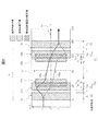
- FIG. 2 shows an example of the configuration of the aberration corrector 6 in the present invention.
- the second- and third-stage electromagnetic multipoles are separated into magnetic multipoles 21b and 24b and electrostatic multipoles 22b and 23b, and the magnetic multipoles and electrostatic multipoles are separated from each other.
- the example which shifted the position which acts is shown. Due to the requirement of maintaining the pole configuration and excitation symmetry and antisymmetry with respect to the corrector center plane 15, the electrostatic multipole 22b is + w in the z direction with respect to the magnetic multipole 21b in the second stage, and the third stage. Similarly, 23b is arranged with a displacement of ⁇ w with respect to 24b.
- the electrons passing through the corrector 6 are branched in the x and y directions by the first quadrupole 20 as in the case of the conventional antisymmetric quadrupole corrector and follow the trajectories of 100x and 100y, respectively.
- the orbits 100x and 100y pass through the second group of multipoles 21b and 22b and the third group of multipoles 23b and 24b with symmetry. That is, in the second group 21b and 22b, the x trajectory passes with a distance from the central axis 16, while the y trajectory passes relatively near the central axis 16.
- the x orbit is in the vicinity of the central axis 16 and the y orbit is away from the axis and passes through them in an antisymmetric manner with respect to the second group passage.
- Negative chromatic aberration is generated in the x direction in the second group multipoles 21b and 22b and in the y direction in the third group multipoles 23b and 24b. Based on the symmetry between the multipole and the orbit, the electron beam is emitted from the corrector 6. Occasionally, negative chromatic aberrations that are equivalent in both the x and y directions, that is, rotationally symmetric, are given. By correcting this negative chromatic aberration with the positive chromatic aberration of the objective lens 11, chromatic aberration correction is realized. The effect of the aberration corrector configuration of the present invention in FIG. 2 in correcting chromatic aberration will be described later with reference to FIGS. 4, 5, 6A and 6B.
- the aberration corrector 6 of FIG. 2 it is possible to correct aperture aberrations including parasitic aberrations up to the third order by appropriately superimposing a dipole field, a hexapole field, and an octupole field with multipoles at each stage. is there.
- the second and third multipoles are separated into electrostatic and magnetic field type multipoles, respectively. Only 21b, 24b and 25cm are sufficient.
- the electrostatic multipoles 22b and 23b can be configured mechanically as quadrupoles so as to form a pure quadrupole field.
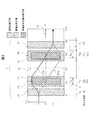
- FIG. 3 shows another example of the configuration of the aberration corrector 6 according to the present invention.
- the second- and third-stage electromagnetic composite multipoles are separated into magnetic-type multipoles 21c and 24c and electrostatic multipoles 22c and 23c, and the working widths of both are changed.
- the second group of magnetic multipoles 21c and the electrostatic multipole 22c are the corresponding magnetic field multipoles of the third group. It has the same width as 24c and electrostatic multipole 23c.
- the electrons passing through the corrector 6 are branched in the x and y directions by the first quadrupole 20 as in the case of the aberration corrector having the configuration shown in FIGS. 8 and 2, and follow the trajectories of 100x and 100y, respectively. Pass through the corrector.
- the orbital symmetry of the x orbit 100x and the y orbit 100y is also the same as that of FIGS. 8 and 2, and therefore negative in the x direction in the second group multipoles 21c and 22c and negative in the y direction in the third group multipoles 23c and 24c.
- Chromatic aberration is generated, and the electron beam is given negative chromatic aberration that is equivalent in both x and y directions, that is, rotationally symmetric, when emitted from the corrector 6 based on the symmetry between the multipole and the orbit.
- chromatic aberration correction is realized.
- FIG. 4 shows the chromatic aberration coefficient when the intensity ⁇ 2E of the two electrostatic quadrupoles 22b and 23b in the aberration corrector 6 is changed while maintaining the symmetry condition between the x orbit 100x and the y orbit 100y under the conditions shown in Table 1.
- the change of CC is compared and plotted with the configuration of the invention of FIG. 8 or FIG.
- the symmetry condition between the x-orbit 100x and the y-orbit 100y is as shown in FIGS. 8 and 2, but it can be expressed as the following equation (6).
- z m is the z coordinate of the center plane 15 of the aberration corrector 6, and shows that the differentiation of the second equation takes on z.
- the overlapping width w of the magnetic quadrupoles 21b, 24b and the electrostatic quadrupoles 22b, 23b in the second group and the third group is 5 (mm) here.
- the vertical axis shows the chromatic aberration coefficient C C / f 2 normalized by the focal length f of the imaging lens.
- the chromatic aberration coefficient 501 corresponding to the configuration of the present invention is smaller than the chromatic aberration coefficient 502 compared to the conventional configuration. More gradual. This is because the chromatic aberration corrector configured as shown in FIG. 2 of the present invention is less sensitive to variations in the electric field quadrupole intensity ⁇ 2E , and conversely, the aberration corrector configured as shown in FIG. It can be said that it is stable against power supply fluctuations that excite the electric field quadrupole. That is, as an effect of the present invention, the stability required for the power source for driving the multipole can be relaxed.
- the chromatic aberration corrector In a charged particle optical system that normally performs chromatic aberration correction by SEM or the like, positive chromatic aberration to be corrected by an objective lens or the like takes a constant value or a value within a limited range. Therefore, it is sufficient for the chromatic aberration corrector to generate a negative aberration sufficient to cancel this.
- the maximum value of negative chromatic aberration obtained by adjusting the overlapping width w of the electrostatic quadrupole and magnetic quadrupole of the second group and third group is set as the corrected chromatic aberration. Can be adjusted to the amount. Furthermore, since the change of the aberration coefficient C C with respect to the variation of ⁇ 2E becomes small in the vicinity of the condition, as a result, more stable chromatic aberration correction can be realized as compared with the conventional case.
- FIG. 5 shows the power supply stability when the aberration corrector shown in the configuration of the invention of FIG. 2 is moved under the conditions shown in Table 1 as in FIG. That is, on the vertical axis, the power supply stability required to excite each multipole is plotted against the overlap width w of the electrostatic quadrupole and the magnetic quadrupole.
- the required power supply stability on the vertical axis is indicated by the logarithmic axis.
- the graph shows the stability of the power supply for the first quadrupole 20, the second group of magnetic quadrupoles 21b and the electrostatic quadrupole 22b with respect to w. Due to the anti-symmetric excitation conditions of the quadrupoles on the plane of symmetry, the third group of magnetic quadrupoles 24b and electrostatic quadrupoles 23b and fourth quadrupoles 25 are also required to have the same power supply stability as the quadrupoles at symmetrical positions. Will be.
- FIGS. 6A and 6B show structural examples for mechanically manufacturing the aberration corrector 6 having the configuration of the invention of FIG. They are a sectional view in the vertical plane and a sectional view in the horizontal plane, respectively.
- the electromagnetic composites 21-22 and 23-24 in the conventional configuration of FIG. 8 are separated into separate electrostatic quadrupole rods 22b and 23b and magnetic field quadrupoles 21b and 24b, respectively.
- FIGS. 6A and 6B show an example in which the center portion through which electrons pass through the liner tube 250 is sealed in a vacuum, and only the electrostatic quadrupoles 240a and 243a are disposed in the vacuum.
- the components of the optical system are not limited to the liner tube 250 as long as a configuration is possible in which the electron path is evacuated and the pole is placed outside the vacuum. Here, they are collectively referred to as an electron vacuum path.
- vacuum here includes not only an ideal vacuum state but also a state where the pressure is reduced to a certain extent so that a charged particle beam can actually pass through the vacuum.
- the liner tube 250 is made of a non-magnetic material, all the magnetic quadrupoles can be placed outside the liner tube 250 and outside the vacuum.
- the first and fourth quadrupoles also use magnetic quadrupoles, and these magnetic poles 200a, 230a, etc. are also in the second group and third group magnetic quadrupoles 210a, 220a.
- an example of installing outside the liner tube 260 is shown. With such a structure, it is not necessary to take a vacuum sealing measure such as an O-ring between each magnetic pole such as 200a and the support member 260, and there is an effect that the vacuum sealing portions can be greatly reduced.
- vacuum sealing with O-rings 251 and 253 or the like may be provided at the upper and lower ends of the liner tube 250 and the introduction of the voltage line for exciting the electrostatic quadrupole.
- FIG. 6A and FIG. 6B in order to clarify the correspondence between the electrostatic electrodes 240a and 243a and the voltage lines 241a and 244a, it is shown that they are individually introduced at each pole position. It may be introduced from one place. Therefore, according to the structural example shown in FIGS. 6A and 6B, the number of vacuum sealed locations in the aberration corrector, which is 70 or more in FIGS. 9A and 9B, can be reduced to a minimum of 3 compared to the conventional configuration. it can. As a result, the magnetic 12-pole can adopt a structure with higher rigidity, and as a result, the mechanical assembly accuracy of the part can be improved.
- the structure of the aberration corrector of FIGS. can be carried by a type multipole.
- FIG. 6A and FIG. 6B assume this, and an example in which these magnetic field type multipoles are composed of 12-poles 210 (a) to 210 (l), etc. is shown.
- the electrostatic multipole placed in a vacuum need only be able to generate only the quadrupole field necessary for chromatic aberration correction, so the mechanical configuration itself can be made a quadrupole.
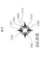
- FIGS. 7A and 7B An example of the structure of the electrostatic quadrupole part in this case is shown in FIGS. 7A and 7B. They are a sectional view in the vertical plane and a sectional view in the horizontal plane, respectively.
- the two quadrupoles 240a, 243a, etc. are respectively installed on one quadrupole support member 261 with insulating thin plates 242a, 245a, etc. sandwiched between the electrodes in the quadrupole and the quadrupole.
- the quadrupole support 260 can be formed of a non-magnetic metal, and the insulating thin plate may be any insulating material having a withstand voltage performance of about ⁇ 100 V. Possible use. As described above, the two quadrupoles are configured as four quadrupoles 240a to 240d and 243a to 243d (243b to 243d are not shown in the figure) as simple quadrupoles. By introducing the electrostatic quadrupole part integrated as described above into the vacuum of the liner tube 250 mm, it is possible to install two electrostatic quadrupoles with high mechanical accuracy.
- those of the third and lower order use four-stage magnetic 12-poles 200a, 210a, 220a, 230a etc. arranged outside the vacuum. Can be compensated.
- a structure (vacuum path) in which magnetic twelve poles are arranged outside the vacuum as shown in FIGS. 6A and 6B can be provided with a mechanism capable of mechanically adjusting the position of each twelve pole in the horizontal plane. .
- the center of the electrostatic quadrupole field and the center of the magnetic quadrupole field formed by the magnetic twelve pole can be realigned, thus further contributing to stabilization of chromatic aberration correction. it can.
- As a mechanism for driving the fine position adjustment of the order of 1 ⁇ m or less necessary for this use of an actuator using a piezo element can be mentioned.
- an effect can be expected even if a mechanical push screw mechanism used for position adjustment of a conventional electromagnetic lens is used for the position adjustment.
- At least two electromagnetic composite quadrupoles used in conventional antisymmetric quadrupole color and spherical aberration correctors are separated into magnetic quadrupoles and electrostatic quadrupoles. Shift the position.
- an antisymmetric multiple quadrupole color / spherical aberration corrector configured to change the width between the two is used.
- the structure of the aberration corrector such as the reduction of the vacuum sealed portion, can be greatly simplified.
- the improvement of the rigidity and mechanical accuracy of the electrostatic multipole element and the magnetic field type multipole element can be expected.
- the structure illustrated in FIGS. 6A and 6B is possible in which only the electrostatic multipole is disposed in a vacuum and the magnetic multipole is installed outside the vacuum.
- a magnetic multipole outside the vacuum is composed of 12 poles and a simple quadrupole is used as the electrostatic multipole placed in the vacuum, all the third-order aperture aberration is compensated by the magnetic multipole outside the vacuum.
- the present invention has been described mainly using the quadrupole and the 12-pole. However, it is added that the number of poles of the multipole is not limited to the embodiment without departing from the spirit of the present invention. Keep it.
Landscapes
- Chemical & Material Sciences (AREA)
- Analytical Chemistry (AREA)
- Electron Beam Exposure (AREA)
Abstract
荷電粒子装置において分解能を向上させるために,収差補正器が大きく期待されている。 一方,低エネルギー電子線を用いる荷電粒子線光学装置では,従来の収差補正器に比べて格段に複雑な構成と,より高い機械精度での組み立てが必要となる。収差補正器で利用される電磁複合四極子部は,極子先端は真空内電子線行路近傍に設置し,励磁コイルは真空外に配置することが望ましく,これら極子毎に電気的絶縁と真空密閉を両立する構造が必要である。このような構造の複雑化は,機械的組立精度の向上とは一般的に相反する。 従来の収差補正器で用いられていた電磁複合多極子おける電極と磁極とを分離し,かつ両者の位置をずらす,或いは両者の幅を一致させないことで,上記課題の複雑な構造を,簡略化できる。従って,機械的組み立て精度の向上を実現できる。
Description
本発明は,荷電粒子線装置に関する発明である。また,荷電粒子線に用いられる収差補正器に関する発明である。
近年多極子収差補正器を用いた電子顕微鏡収差補正技術は,透過電子顕微鏡(TEM),走査透過電子顕微鏡(STEM)では既に一般化しつつある。電子エネルギー100keV以上の高加速TEM,STEMではこの技術を用いて球面収差を補正することで従来困難であった,0.1 nmを切る超高分解能での観察が可能となっている。走査電子顕微鏡においても,高分解能化は従来の対物レンズ形状の最適化,リターディング,ブースティング等の電子行路上のエネルギー最適化では限界に近付いている。従って特にエネルギー1 keV以下の低エネルギー領域で分解能を向上させる手段として,TEM,STEMと同様に多極子収差補正器を用いた収差補正が非常に期待される技術となっている。
ただし,高加速TEM,STEMと異なる点は,SEMで対象とする電子線のエネルギーが低い為に,球面収差と同等或いはそれ以上に色収差が分解能を制限する主要因となることである。このため高加速TEM,STEMで広く用いられる六極子球面収差補正器とは異なる構成の色・球面収差補正器がSEM,低加速TEM・STEM(特に,エネルギー30 keV以下)において求められている。
この目的の為には,これまで H. Rose が提案し,J. Zachらが実効性を実験的に確認した,反対称四重四極子色・球面収差補正器を始めとして,複数の構成の色(球面)収差補正器が提案されている(特許文献1)。これらの収差補正器は2段以上多段の四極子-八極子レンズを基本構成とする。特にこれを構成する多段多極子のうち少なくとも2段の多極子は色収差補正を実施する為に,磁場と静電場の四極子場を同一箇所に発生される電磁複合四極子であることが特徴となる。これらの電磁複合四極子は,さらに球面収差等三次までの開口収差を補正するために,同時八極子,六極子,双極子場を発生できるようなっている場合もある。このため,四極-八極色・球面収差補正器の各多極子は,上記電磁複合四極子だけでなく,実際にはその他の多極子も12極子で構成されることが多い。
従来技術の例として,基本となるH. Rose の反対称四重四極子球面収差補正器の構成を図8に示し,以下その動作原理を説明する。この色・球面収差補正器6は,四段の多極子,20,21と22,23と24,25から構成されており,上記の通りこれらのうち内側の二段は磁界四極子21,23と静電四極子22,24を同一の多極子で発生させる電磁複合四極子である。これら前後の多極子20と25は主な目的として,電磁複合四極子21-22と23-24において色収差補正に適切となる軌道に電子を導くことであり,実効的な色収差補正そのものは二段の電磁複合四極子21-22と23-24を用いて行われる。前後の多極子20,25に関しJ. Zachらは静電四極子を用いたが,これらが磁界四極子であっても構わない。
より具体的に電子は,図8のように収差補正器左方から平行に入射し,軌道 100xと,100yを辿って補正器終端から平行に出射する。補正器入射時と出射時の電子線の中心軸から離軸距離も等しくなるように設定される。そして,収差補正器のオンとオフで補正器外の光学系に影響を与えることなくテレスコピックに利用できるように工夫されている。さらに収差補正器6内部では,まず左方から入射した電子線が第一段の四極子20で,x 軌道100xと,y 軌道100yに分岐され,第二段の電磁複合四極子21-22を,x 軌道100x は軸を離れて通る。一方,y 軌道100y は当該複合四極子のほぼ中心を通るように調整される。場の分布として,矩形場近似を仮定すると第二段の電磁複合四極子内部での電子の運動は,以下の式(1)の運動方程式で記述される。

ここで,L は極子長であり,θ は以下の式(2)のように四極子場強度を表すパラメータである。
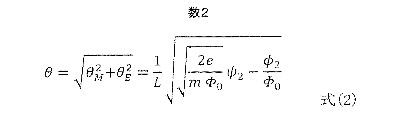
さらにここで,θE とθM は式(2)内で展開される通り,各々静電四極子と磁界四極子強度を表すパラメータである。
式(2)の三項目の係数ψ2 とΦ2 で各々四極子場の磁気ポテンシャルと静電ポテンシャル分布は次式の式(3)となる。

また式(2)で,eとmは,電子の電荷と質量であり,Φ0は収差補正器を通過する際の電子のエネルギーである。電子エネルギーの分布を考慮してΦ0 +δΦ のエネルギーを持つ電子に対して式(2)は,以下の式(4)のように変形される。

上記の式の第三項目への変換では,δΦを微小量としてその一次まで残した。従ってこの近似の式(5)の下で,以下のようになる。
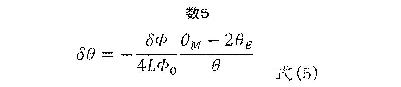
δθ は,電子エネルギーの変化(分布)に対する四極子強度の変化である。つまり,式(2)と式(5)の二式は,電磁複合四極子を用いることで総強度(すなわち,式(2))は一定値を維持しながら,一方分散(すなわち,式(5))を正負任意に調節することが可能であることを意味している。この結果,電磁複合である第二四極子21-22で,x 方向に負の分散を持つ凸レンズを作って,x 軌道100x の電子に負の色収差を与えることが可能である。言い方を変えれば,静電四極子と磁界四極子の電子エネルギーΦ0への依存性が異なるので,x 方向に関して磁界四極子で凸レンズを,静電四極子で凹レンズを形成し,両者打ち消しの残分として負の分散を持つ凸レンズを形成して負の色収差を生み出したとも言える。一方,先に指摘した通り y 軌道100yは第二の四極子21-22においてその中心を通るように調整されているので,100yは収差を含め当該四極子の影響を殆ど受けずにこれを通過する。
同様にして,電磁複合である第三の四極子23-24では,第二・四極子21-22と反対称となるように,x 軌道100xが四極子中心を,y 軌道100yが軸から離れた箇所を通過するように設定される。これらによって,前節とは逆に今度は y 軌道100y に対して負の色収差を与えることができる。ここまで分岐した x 軌道と y 軌道を辿った電子は,第四の四極子25で再びスティグマティックに統合され収差補正器6を出射する。結果として,上記の反対称四重四極子収差補正器はx と y 方向に等量の,従って回転対称かつ正負任意に調整可能な色収差を提供でき,これと当該収差補正器6より光学的下流に位置する対物レンズ11の(正の)色収差を相殺することで,SEM光学系の全体としての色収差補正を実現することができる。
上記に加えて,収差補正器6の四段の四極子各々に適宜な八極子場を重畳して加えることで,球面収差を始めとする三次開口収差の補正が可能となる。さらに同様に適宜六極場,双極場を各段に与えることで,収差補正器内外,光学系の不完全性から現れる一次と二次の寄生収差を補償することもできる。以上をもって,反対称四重四極子収差補正器により,色収差および三次までの開口収差補正が可能となる。
この収差補正器において四段の四極子は,上記 x 軌道と y 軌道に対する対称性を保つため,さらに四次以上の高次収差を対称性によって収差補正器内部で相殺させる。このため,第一段20と第四段25,第二段21-22と第三段23-24は,収差補正器内中心面15に対称に配置され,同時に反対称に励起される。すなわち反対称四重四極子となる。
上記の従来の技術に記述の通り,色収差補正の為には電磁複合四極子を2つ以上含む多段多極子収差補正器を構成し,前記電磁複合四極子が生成する負の色収差と,当該のSEMの対物レンズ等荷電粒子光学系で問題となる正の色収差と相殺せしめることで色収差補正を実現する。
現在まで提案されてきた多くの色・球面収差補正器(例えば特許文献1)も,含まれる多極子の数や光学要素の数は変えながらも,色収差を補正する原理は,上記に述べて電磁複合四極子による負の色収差の生成に基づく。従って,これら電磁複合四極子を含む多段多極子収差補正器は似た特徴を持つと同時に同様の課題を持っている。特に高加速TEM,STEMで既に利用されている六極子球面収差補正器に比べ原理的により高い機械精度を要求される一方で,実際にはより多段の多極子を組み合わせた構造は複雑になり十分な機械的精度を保ちにくくなる。以上は,今も同型式における色・球面収差補正器の実用化に向けて大きな課題となっている。
上記のような従来の色・球面収差補正器で機械的な構造の複雑性は,構成例を図9Aおよび図9Bにされる。特に第二と第三の多極子は電磁複合である必要性から,図9Aおよび図9Bに示すような複雑な構造を持たざるを得ない。即ち,図9Aおよび図9Bで示される通り二段目多極子の多極子は,中心軸14近傍の真空部分に静電四極子場を形成するために,極子210a先端は真空内に露出していなければならない。また,極子間或いは極子と支持材260の間で十分な電気的な絶縁も保たれていなければならない。
一方,極子210aは,同時に磁極でもあるためにこれを励磁するコイル211aを備えなければならない。励磁コイルは,表面積も大きくガス放出の原因になり,かつ通電により発熱もおこるのでなるべく真空外に置くことが望ましい。
これら電子複合四極子におけて機械的構成にかかる要求をまとめると,極子210aの先端は真空中に,かつ210aの他端は励磁コイル211aを備える為に大気側に支持材260を挟んで設置することである。さらに,支持材260と極子210aの間は絶縁スリーブ214aを挟んで電気的絶縁を保つ必要がある。勿論,同箇所において真空密閉も行わなければならないので,電磁複合の極子210aの箇所では極子210aと絶縁スリーブ214a,絶縁スリーブ214aと支持材260の間の両箇所で二重にOリング(断面が円形の環型をした密封用の機械部品)を挟むことになる。このような複雑な多極子構造において,多極子先端の配置精度をμmオーダーに保ちつつ同時に多極子全体にわたって磁気的にも均一な接続を維持しながら,かつ前記のような電気絶縁,真空密閉の機能を満足する構造の実現は非常に困難であると言える。
また,収差補正器構造の複雑化とは別に,高加速TEM,STEM用六極子球面収差補正器に比べて,多段多極子色・球面収差補正器は,電磁複合四極子を含む等の理由で,これを駆動するための電源安定度が一桁以上高いことも問題である。一般に,前者六極子球面収差補正器を駆動させるためには,10-5~10-6の安定度の電源が必要であるとされるのに対して,後者色・球面収差補正器には10-7~10-8より高い安定度の電源が要求される。
従って本発明の一つの課題は,上記の複雑な機械的構造をできるだけ簡易化し,多極子先端の機械的配置精度と多極子全体の磁気的均一性を向上させやすくすることである。
またいま一つの課題は,同種の電磁複合多極子を備える多段多極子色・球面収差補正器に必要な駆動電源の要求電源安定度を,従来に比べて緩和することである。
上記の課題を解決するため、本願発明の1つの形態は、試料に荷電粒子線を照射し,前記試料に起因する荷電粒子を検出する荷電粒子線装置において,第一および第二の磁界型の多極子と,前記第一の磁界型の多極子と第二の磁界型の多極子との間に設けられた第三および第四の磁界型多極子と,前記第一の磁界型の多極子と第二の磁界型の多極子との間に設けられた第一および第二の静電型多極子とを備え,前記第一乃至第四の磁界型多極子と前記第一および第二の静電型多極子とは中心対称面に対して対称に配置されるとともに,それぞれ反対称に励起され,前記第二の磁界型多極子が設けられた第一平面と前記第一の静電型多極子が設けられた第二平面とは異なり,前記第三の磁界型多極子が設けられた第三平面と前記第二の静電型多極子が設けられた第四平面とは異なる,ことを特徴とする収差補正部を前記試料に前記荷電粒子線を照射する経路,もしくは前記試料に起因する荷電粒子を検出する経路に設置する。
また、本願発明の他の形態は、試料に荷電粒子線を照射し,前記試料に起因する荷電粒子を検出する荷電粒子線装置において,第一および第二の磁界型の多極子と,前記第一の磁界型の多極子と第二の磁界型の多極子との間に設けられた第三および第四の磁界型多極子と,前記第一乃至第四の磁界型多極子と前記第一および第二の静電型多極子とは中心対称面に対して対称に配置されるとともに,それぞれ反対称に励起され,前記第二の磁界型多極子が作用する磁場と前記第一の静電型多極子が作用する電場との幅が異なり,前記第三の磁界型多極子が作用する磁場と前記第二の静電型多極子が作用する電場との幅が異なる,ことを特徴とする収差補正部を前記試料に前記荷電粒子線を照射する経路,もしくは前記試料に起因する荷電粒子を検出する経路に設置する。
また、本願発明の他の形態は、試料に荷電粒子線を照射し,前記試料に起因する荷電粒子を検出する荷電粒子線装置において,平面に設けられた多極子を4以上の段数にて有する収差補正部を有し,第一の平面に設けられた第一の磁界型多極子と,前記第一の平面よりも下方となる第二の平面に設けられた第一の静電型多極子と,前記第二の平面よりも下方となる第三の平面に設けられた第二の静電型多極子と,前記第三の平面よりも下方となる第四の平面に設けられた第二の磁界型多極子と, 前記第一の磁界型多極子と前記第二の磁界型多極子との間に設けられ,前記収差補正器の中心対称面に対して反対称に励起される第一及び第二の磁界型素子と,を有し前記収差補正器は,前記第一の静電型多極子が生じさせる第一の電場と前記第一の磁界型素子が生じさせる第一の磁場とが重畳する第一の場と,前記第一の電場と前記第一の磁場とのどちらかが単独にて作用する第二の場と,前記第二の静電型多極子が生じさせる第二の電場と前記第二の磁界型素子が生じさせる第二の磁場とが重畳する第三の場と,前記第二の電場と前記第二の磁場とのどちらかが単独にて作用する第四の場と,を形成することを特徴とする収差補正部を前記試料に前記荷電粒子線を照射する経路,もしくは前記試料に起因する荷電粒子を検出する経路に設置する。
また、本願発明の他の形態は、第一および第二の磁界型の多極子と,前記第一の磁界型の多極子と第二の磁界型の多極子との間に設けられた第三および第四の磁界型多極子と,前記第一の磁界型の多極子と第二の磁界型の多極子との間に設けられた第一および第二の静電型多極子とを備え,前記第一乃至第四の磁界型多極子と前記第一および第二の静電型多極子とは中心対称面に対して対称に配置されるとともに,それぞれ反対称に励起され,前記第二の磁界型多極子が設けられた第一平面と前記第一の静電型多極子が設けられた第二平面とは異なり,前記第三の磁界型多極子が設けられた第三平面と前記第二の静電型多極子が設けられた第四平面とは異なることを特徴とする収差補正器である。
また、本願発明の他の形態は、第一および第二の磁界型の多極子と,前記第一の磁界型の多極子と第二の磁界型の多極子との間に設けられた第三および第四の磁界型多極子と,前記第一乃至第四の磁界型多極子と前記第一および第二の静電型多極子とは中心対称面に対して対称に配置されるとともに,それぞれ反対称に励起され,前記第二の磁界型多極子が作用する磁場と前記第一の静電型多極子が作用する電場との幅が異なり,前記第三の磁界型多極子が作用する磁場と前記第二の静電型多極子が作用する電場との幅が異なることを特徴とする収差補正器である。
本発明を用いることで、複雑な機械的構造が簡易化され,多極子の精度を向上させることができる。
本発明は,高分解能を要する荷電粒子光学装置,特に色収差がその分解能制限の主要因となるような低エネルギーの荷電粒子を用いる装置に関するもので,従来より要求電源精度が緩く,かつ機械的構成が簡単な色・球面収差補正器を提供するものである。特に限定するわけではないが,低加速走査電子顕微鏡(SEM),走査透過電子顕微鏡(STEM)での利用を念頭に以下に記述する。
本願発明が提示する基本的な解決手段は,従来の多段多極子色・球面収差補正器に含まれる電磁複合多極子を個別の静電型多極子と磁界型多極子に分離し,かつ両者の電子線行路上の位置もしくは幅に差分を設けることである。これによりまず前述の通り構造の複雑な電磁複合多極子を廃し,単純な静電型多極子と磁界型多極子を真空の内外に分けて配置することが可能となる。これにより,電磁複合多極子を構成するに要した複雑な電気絶縁と真空密閉構造を避けることができ、簡略化を見込むことができる。これに応じて,機械的な多段多極子収差補正器の組み立て精度の向上も見込むことができる。本願発明による多段多極子色・球面収差補正器の具体的な構成例は,図6A,B,図7A,B を用いて追って説明する。
本願に係る荷電粒子線装置は,具体的には、試料に荷電粒子線を照射し,これに従い前記試料から発生する荷電粒子や電磁波等の信号を検出する荷電粒子線装置とし,試料上の荷電粒子線照射径をより小さく絞るための多段多極子色・球面収差補正器を備えるものとする。前記多段多極子色・球面収差補正器は,その両端もしくは両端に近い位置に少なくとも四極子場を発生する対となる二つの磁界型多極子を備え,前記磁界型多極子対の間に,さら対となる2つの磁界型多極子と,前記4つの磁界型多極子とは異なる対となる2つの静電型多極子とを備える構造を基本構成とするものである。
以下記述の便宜上,前記四つの多極子は荷電粒子線の入射端から出射端に向かって準に第一乃至第四の磁界型多極子と呼び,同様に2つの静電型多極子も入射端側から順に第一と第二の静電型多極子と呼称することにする。対となる第一と第四の磁界型多極子,第二と第三の磁界型多極子,および第一と第二の静電型多極子は,収差補正器の中心面に対して各々対称に配置され,かつ反対称な強度の四極子場を形成する機能を有するものとする。ここで,第二の静電型多極子と第一磁界型の多極子,或いは第三の静電型多極子と第二の磁界型多極子が荷電粒子行路上の同一箇所に同一分布の四極子場を形成するため,各々静電型と磁界型多極子の両者で共通の極子を用いる構造とすると,前述の電磁複合型多極子となる。この場合,実装するための構造が複雑になり要求される機械精度を充足し難くなることは本願の課題の欄で説明したとおりである。
よって,本願にかかる第一の手段は,上記の収差補正器中心面に対する配置の対称性,励起の反対称性は維持したまま,第二の磁界型多極子と第一の静電型多極子,従って第三の磁界型多極子と第二の静電型多極子を荷電粒子行路上で完全には重畳しない位置に配置することである。これには,第二の磁界型多極子と第一の静電型多極子が(対称性を維持するように第三の磁界型多極子と第二の静電型多極子も)部分的に重なりを持って配置される場合も含む。
また,本願にかかる第二の手段は,上記の収差補正器中心面に対する配置の対称性,励起の反対称性は維持したまま,第二の磁界型多極子と第一の静電型多極子,従って第三の磁界型多極子と第二の静電型多極子の極子長(荷電粒子行路に沿った多極子の作用長)に差を持たせ,当該の静電多極子と磁界型多極子両者の多極子場の分布に差分を持たせることである。あるいは,本願にかかる別の手段は上記第一と第二の手段を兼ね合わせ,第二の磁界型多極子と第一の静電多極子の,従って第三の磁界型多極子と第二の静電型多極子の位置および極子長を共に変えることである。
本発明を適用することで,構造の複雑な電磁複合多極子を排除し,静電多極子と磁界型多極子の組に置き換えることができる。静電型多極子本体を真空内に設定する一方,非磁性材料の真空容器を用いれば磁界型多極子を励磁に必要なコイル群と合わせて真空外に配置でき,電磁複合型多極子で必要とされた複雑な電気絶縁,或いは真空密閉の為の複雑な構造を大幅に簡略化できる。これにより静電型多極子と磁界型多極子各々において,機械精度の向上を図ることが可能となる。
さらに,第二(第三)磁界型多極子と第一(第二)静電型多極子の重複長,或いは両者極子長の差分という新しい任意調整可能なパラメータを導入することにより,これを利用して色収差補正量とこれに必要な駆動電源電流/電圧の関係を調節可能となる。発明の具体例にて詳述する通りこれを調節することにより,色収差補正に必要な電源の要求安定度の緩和することも可能となる。
また,本発明の他の課題としては,当該補正器を駆動する電源に要求される安定度や精度の高さを緩和することがある。具体的な数値は多段多極子収差補正器の実際の構成や,これを用いる荷電粒子線装置の構成,補正対象とする荷電粒子の種類,エネルギー等によって変化するが,電磁複合四極子を色収差補正に利用する従来の多段多極子色球面収差補正器では、背景技術の欄で色収差補正の原理として説明した通り、電磁複合多極子にて発生する磁界四極子の凸レンズと静電四極子の凹レンズの相当部分を相殺させ残余に残るレンズ作用として負の色収差を実現する。
実用的に十分な精度の負の色収差を得るためには,従って元となる磁界四極子と静電四極子にはより高い精度を求める必要があることが理解できる。実際の例としてこれまでに開発されてきた収差補正器において、高加速TEM,STEM用六極子球面収差補正器を駆動させるには δI / I ≒ 10-5~10-6の安定度の電源が必要とされたのに対し,電磁複合四極子を用いる多段多極子色・球面収差補正器においてはこれより高い δ V / V ,δ I / I ≒ 10-7~10-8の安定度の電源が必要とされてきた。ここで,δ V / V ,δ I / I はリップルを含めた電圧源,電流源の要求安定度を示している。
これに対して本願発明においては、電磁複合多極子を個別の磁界型多極子と静電型多極子に分離した結果,これらの位置と幅の差分を調整パラメータとして色収差補正に必要とする電源精度を調節し,条件によっては40~50%緩和できることを見いだせた。
以下本発明の詳細を各図面に沿って説明する。
まず,図1は,本発明のような多段多極子収差補正器を搭載するSEMの一般的な装置構成を示す。SEMの鏡筒部分1には電子源を含む電子銃3と,これを発した電子を収束,試料12上に縮小投影して微小電子プローブを形成するための対物レンズ11および、対物レンズまで電子を適切な軌道で送る収束レンズ4,中間レンズ7(第二収束レンズ)を電子銃3と対物レンズ12の間に備える。収束レンズ4はさらに縮小率を上げる等の目的でより多段で用いられることもあり得る。
また,上記の通り形成された電子プローブを試料面上で走査(ラスタースキャン)させるための走査コイル10を備え,電子プローブによって試料面から発する二次電子,反射電子を検出する検出器9を備える(図1で検出器9は,二次電子検出器を例示している)。試料12は試料室2内で,水平移動や傾斜が可能な試料ホルダ13の上に設置され観察される。前記電子プローブで試料面を走査して得られる二次電子等の強度は,制御コンソール50に送られ,再びラスタースキャンに応じて二次元にマッピングされ,即ちSEM画像として観察記録することができる。なお,ここでいう制御コンソール50には制御部および入出力部が含まれる。
このようなSEMの場合多段多極子収差補正器6は,主として対物レンズ11の色収差と球面収差を補正するために,対物レンズ11の上流に置かれる。さらに,収差補正器6と対物レンズ11の間の結合収差の発生を抑制する目的から,図1のようにさらに中間レンズ7の上に設置されることが多い。この収差補正器6は収差補正制御電源51で駆動されるが,収差補正制御電源51自体のコントロールは電子顕微鏡本体制御52と同一,もしくは独立した制御部を用いて行われる(もしくは上述した制御コンソール50に含まれてもよい)。図1の場合は両者が同一の制御コンソール50によってコントロールされる場合を例示した。他に,SEMには必要に応じてブースティングやリターディング等の電子エネルギー調整機構,EDX等例示以外の信号検出器が付属する場合もある。図1では省略しているが,本願発明の範囲内にてこれらの光学系を追加できることは言うまでもない。
図8は,前述の通り従来の多段多極子色・球面収差補正器の例として,反対称四重四極子収差補正器の構成を示した。図8で示した構造と収差補正原理は従来の技術に含まれる。図に示される通り四段の多極子が収差補正器6の中心面15を対称面として対称に配置され,うち第二段21-22と第三段23-24は色収差補正の為に電磁複合多極子である。これらも含め四段の多極子は中心面15に対して反対称な反対称四重四極子を励起する。収差補正器6内で電子は,第一段の四極子20でx 軌道100xとy 軌道100yにアスティグマティックに分岐されてそれぞれ反対称な軌道を辿り,既に説明した通り電磁複合四極子を形成する第二段多極子21-22で x 方向の,第三段多極子23-24で負の色収差を与えられる。
上記の極子配列及び励起の対称性から,x と y 方向に与える負の色収差は等量であり,即ち回転対称である。これらx 軌道100xとy 軌道100yは第四段多極子25で再び回転対称となるように統合される。以上の過程で収差補正器6によってつくられた負の色収差と,対物レンズ11の正の色収差を相殺せしめることで,色収差補正が実現されるのは前述の通りである。同様に,四段の多極子に適宜双極子場,六極子場,八極子場を重畳することで,球面収差を始め,系の不完全性による寄生収差を含む三次までの開口収差を補正することができる。
一方,図2は,本眼発明における収差補正器6の構成の一例を示している。この図2の例では,第二段と第三段の電磁複合多極子を磁界型多極子21b,24bと静電多極子22b,23bに分離し,かつ磁界型多極子と静電多極子とが作用する位置をずらした例を示している。補正器中心面15に対する極子構成と励起の対称性,反対称性を維持する要求から,第二段で静電多極子22bは,磁界型多極子21bに対して z 方向に+w,第三段で同様に23bは24bに対して-w 変位して配置される。
補正器6を通過する電子は,従来の反対称四重四極子補正器における場合と同様に第一の四極子20で x 方向と y 方向で分岐され,それぞれ100xと100yの軌道を辿って補正器内を通過する。100xと100yの軌道は,第二群の多極子21bと22bと第三群の多極子23bと24bを,対称性を持って通過する。即ち第二群21bと22b では,x 軌道が中心軸16から距離をもって通過するのに対してy 軌道は比較的中心軸16の近傍を通過する。第三群23bと24bにおいては,第二群通過と反対称的にx 軌道が中心軸16近傍,y 軌道が軸から離れてこれらを通過する。
第二群多極子21b,22bにおいてx 方向,第三群多極子23b,24bにおいてy 方向に負の色収差を発生し,上記多極子と軌道の対称性を元に,電子線は補正器6出射時にx,y 両方向に等値な,即ち回転対称な負の色収差を付与されることになる。この負の色収差を対物レンズ11の正の色収差と相殺させることで,色収差補正は実現される。色収差補正における図2の本発明での収差補正器構成における効果は,図4,図5および図6Aおよび図6Bにおいて追って説明される。
図2の収差補正器6においても,各段の多極子で適宜双極子場,六極子場,八極子場を重畳すれば,三次までの寄生収差含む開口収差を補正出来ることは従来と同様である。この例では第二と第三の多極子を静電と磁界型多極子にそれぞれ分離しているが,開口収差補正の為に八極子等を重畳して掛ける多極子は磁界型多極子 20 ,21b,24b,25 だけで十分である。静電多極子22bと23bは,純粋に四極子場を形成するよう機械的にも四極子として構成することも可能である。
図3は,本発明による収差補正器6の構成のまた別の一例を示している。この図3の例では,第二段と第三段の電磁複合多極子を磁界型多極子21c,24cと静電多極子22c,23cに分離し,かつ両者の作用する幅を互いに変える例を示している。補正器中心面15に対する極子構成と励起の対称性,反対称性を維持する要求から,第二群の磁界型多極子21cと静電多極子22cは,第三群の対応する磁界型多極子24cと静電多極子23cと同じ幅をそれぞれ持っている。
補正器6を通過する電子は,図8や図2の構成の収差補正器の場合と同様に第一の四極子20で x 方向と y 方向で分岐され,それぞれ100xと100yの軌道を辿って補正器内を通過する。x 軌道100xと y 軌道100yの軌道の対称性も図8,図2と同様であり,従って第二群多極子21c,22cにおいてx 方向,第三群多極子23c,24cにおいてy 方向に負の色収差を発生し,上記多極子と軌道の対称性を元に電子線は補正器6出射時にx ,y 両方向に等値な,即ち回転対称な負の色収差を付与されることになる。この負の色収差を対物レンズ11の正の色収差と相殺させることで,色収差補正は実現される。
図3の収差補正器6においても,図2の構成で説明したと同様に各段の多極子に適宜双極子場,六極子場,八極子場を重畳すれば,三次までの寄生収差含む開口収差を補正出来る。また,開口収差補正の為に八極子等を重畳して掛けるのは,磁界型多極子 20 ,21c,24c,25 だけで十分であり、図2の例と同様に静電型多極子は純粋に四極子場を形成するよう機械的にも四極子として構成することも可能である。
図4と図5において,本発明の収差補正器構成よる効果を説明する。これらに示す結果は,図2に示した収差補正器の構成例を元に,以下に示す表1のパラメータを用いて計算したものである。四極子場の分布には矩形場近似を仮定した。

図4は,表1の条件でx 軌道 100xとy 軌道100y の間の対称条件を維持して収差補正器6内の二つの静電四極子22bと23bの強度 θ2E を変える場合の色収差係数CC の変化を,図8や図2の発明の構成で比較してプロットしている。x 軌道 100xと y 軌道100y の間の対称条件は,図8と図2に見られる通りであるが,式として記述すると以下の式(6)となる。

ここで,zmは収差補正器6の中心面15の z 座標であり,また第二式の微分は z に対して取ることを示している。本願発明の構成の場合,第二群と第三群の中での磁界四極子 21b,24bと静電四極子22b,23bの重複幅 w は,ここでは5(mm)とした。縦軸は,結像レンズの焦点距離 f で規格化した色収差係数CC/f2 を以て示している。
図4のグラフにみるように,図8の従来構成収差補正器に対する色収差係数 502 と図2に示した本願発明構成の収差補正器に対する色収差係数 501はθ2E= 0 ではいずれも正値であるが,θ2Eの増加に従って値が減少し,やがて負の値を取るようになるが,特に従来の構成に対する色収差係数 502 に比較して本願発明の構成に対応する色収差係数 501 の方の減少がより緩やかである。これは本願発明図2の構成の色収差補正器の方が,電界四極子強度θ2Eの変動に対して鈍感であり,逆に見れば本願発明の図2に示す構成の収差補正器の方が電界四極子を励起する電源変動に対して安定的であると言える。即ち、本発明の効果として、多極子を駆動する電源に要求される安定度を緩和出来たことになる。
上記の差は,定性的には以下のように説明できる。第二段と第三段に電磁複合四極子21-22,23-24を用いることによって,静電と磁界四極子場の分布が一致している図8の従来の構成では,電源容量や耐電,極子の磁気飽和等物理的制限に因らない限りθ2E の増大に対してCC は単調に減少する。そして,原理的にはいくらでも大きな負の色収差を得ることが可能である。一方,わざと電磁複合四極子を静電四極子22b,23bと磁界四極子21b,24bに分離し,両者の作用位置をずらした図2の本願発明の構成においては,静電四極子22b,23bと磁界四極子21b,24bが重複する w の範囲では従来と同じ原理で負の色収差が発生するが,その外側静電四極子場もしくは磁界四極子場しか存在しない領域ではむしろ負の色収差発生を抑制される。この結果,図2の発明の構成ではθ2E を増大させても,静電と磁界四極子の重複幅wに依存して色収差係数CC がある最低値以下には減少しなくなる。例えば,表1の計算条件の下では,w < 2.4(mm)ではθ2Eを増大させても,CC は負の値を取れなくなる。以上の結果,図2の発明の構成の収差補正器では,θ2Eの増大に対するCC の減少が緩やかになり,前節に述べた効果を得ることが可能となる。
通常SEM等で色収差補正を行う荷電粒子光学系では,対物レンズ等による補正すべき正の色収差は一定値もしくは限定された範囲の値を取る。従って,色収差補正器としてはこれを相殺するに十分な負の収差を発生できれば十分である。図2の本願発明の構成の収差補正器では第二群,第三群の静電四極子と磁界四極子の重畳幅w を調節することで得られる負の色収差の最大値を,被補正色収差量に合わせて調整できる。さらに当該条件の近傍ではθ2E の変動に対する収差係数CC の変化が小さくなるので,これらの結果従来に比較してより安定した色収差補正を実現できることになる。
図5では,図4と同じく図2の発明の構成に示す収差補正器を表1の条件の下動かす時の電源安定度を示している。すなわち縦軸には,各々多極子を励起するに要求される電源安定度を,静電四極子と磁界四極子の重複幅 w に対してプロットしている。図5のグラフの左端が図4のグラフに示した図2の発明の構成の収差補正器でw = 5(mm)に対応するものであり,グラフ右端ではw = L2E = L2M = 10(mm)と静電四極子と磁界四極子が全幅重複する条件であるからこれは図8の従来の構成の収差補正器と等価である。
縦軸の要求電源安定度は,対数軸で示している。グラフには第一の四極子20と第二群の磁界四極子21b及び静電四極子22bにかかる電源の安定度をw に対して表示しているが,収差補正器6の中心面15を対称面とする四極子の反対称励起条件から,第三群の磁界四極子24b及び静電四極子23bと第四四極子25についても各々対称な位置にある四極子と同じ電源安定度が要求されることになる。
図5から,まず図8の従来の構成と図2の発明の構成の収差補正器において,以下の共通点が確認される。まず,第一(第四)四極子に比較して,第二もしくは第二群(第三もしくは第三群)の各々四極子を励起する為の電源により厳しい電源安定度が要求されている。また,前述したように,もっとも厳しい第二群磁界四極子に対する要求電源安定度は,10-7(10の-7乗)のオーダーとなっていることがわかる。
以上は,図2の発明の構成に基づくモデルでの計算結果を示した。図示は省略したが,同様に静電四極子と磁界四極子の幅を変える図3に示す別の構成を用いても,図4で述べた色収差補正の安定化,図5で見た要求電源安定度の緩和の効果を得ることが計算で確認された。
一方,静電四極子と磁界四極子の重複幅 w に対する要求電源安定度の変化をみると, w が小さくなるほど全幅重複,即ち図8の従来の構成での収差補正器に対して,要求電源安定度が緩和されることが見て取れる。特に,極子のうちでもっとも厳しい電源安定度が要求される第二群磁界四極子21bに対しては,従来の構成(w = 10(mm))では0.45 ppm 以下の電源安定度が必要とされるところ,重複幅をw = 5(mm)まで減らすと要求が二倍弱(0.80 ppm以下)までに緩和される。この理由は,図4に対して定性的ながら説明した色収差補正の安定化原因と対応する。
図6Aおよび図6Bは図2の発明の構成の収差補正器6を機械的に製作するための構造例を示す。それぞれ,垂直平面での断面図と水平面での断面図である。図2の発明の構成における収差補正器では図8の従来の構成での電磁複合21-22と23-24は,各々別の静電四極子 22b,23bと磁界四極子21b,24bに分離され別々に配置することができる。特に図6Aおよび図6Bでは,ライナーチューブ250にて電子を通す中心部を真空で密閉し,静電四極子240a,243a のみ真空内に配置する例を示している。なお,電子の通路を真空にし,極子を真空外に置く構成が可能であれば,光学系の部品はライナーチューブ250に限定されるものではない。ここではそれらを総称して電子の真空経路部と呼ぶ。また,ここでいう真空とは理想的な真空状態だけでなく,現実的に荷電粒子線が通過できるような,ある程度まで減圧された状態も真空の定義に含めている。
ライナーチューブ250を非磁性材料で作成すれば,磁界四極子すべてはライナーチューブ250の外側,真空外に置くことができる。この利点を持って,図6Aおよび図6Bでは第一と第四四極子も磁界四極子を用いるとし,これらの磁極子200a,230a等も第二群,第三群の磁界四極子210a,220aとともにライナーチューブ260の外に設置する例を示している。このような構造にすれば,200a等各々の磁極子と支持材260の間でOリング等の真空密閉策を取る必要がなく,大幅に真空密閉箇所を削減できる効果がある。
具体的には,ライナーチューブ250の上下端と,静電四極子を励起するための電圧線の導入箇所でOリング251,253等による真空密閉を講じればよい。図6Aおよび図6Bでは,静電極子240a,243a等と電圧線241a,244a等の対応を明確にするために各々の極子位置で個別に導入するよう示しているが,実際には電圧線は一箇所から纏めて導入しても構わない。よって,図6Aおよび図6Bに示す構造例に従えば,従来の構成に比べて,図9Aおよび図9Bで70箇所以上あった収差補正器内での真空密閉箇所を最低3箇所まで減らすことができる。これにより,磁気12極子はより剛性が高い構造を採用でき,結果として当該部の機械的な組み立て精度の向上を実現できる。
さらに図2の発明の構成における収差補正の原理の説明でも触れたように,図6Aおよび図6Bの収差補正器の構造であれば,三次までの開口収差を補正する役割をすべて4段の磁界型多極子に担わせてしまうことができる。
図6Aおよび図6Bではこれを想定し,これら磁界型多極子を12極子210(a)から210(l)等で構成する例を示した。この場合,真空内に置かれた静電多極子は,単純に色収差補正に必要な四極子場のみ発生出来ればよいので,その機械的構成自体を四極子にしてしまうことが可能である。この場合の静電四極子部の構造例を図7Aと図7Bに示した。それぞれ,垂直平面での断面図と水平面での断面図である。二つの四極子240a等と243a等は各々四極子内の電極と四極子相互の配置精度を高めるために,一つの四極子支持材261に絶縁薄板242a,245a等を挟んで設置されている。
また,四極子支持材260は,非磁性金属で形成可能であり,絶縁薄板は ~100 V 程度の耐電性能を持つ絶縁材料であれば構わないが機械精度を高める為硬度の高いセラミック薄板等の利用が考えられる。二つの四極子は前述の通り単純四極子として四つの極子240aから240d,243a から243d (243b から243dは図に非表示)で構成する。以上のように一体化した静電四極子部をライナーチューブ250 の真空内に導入することで,高い機械精度で2つの静電四極子を設置することが可能となる。さらにこれ以上,静電四極子部の機械精度不足等によって寄生収差が発生するならば,三次以下のそれらは真空外に配置された四段の磁気12極子200a,210a,220a,230a等を用いて補償することができる。
図6Aおよび図6Bに示すような磁気12極子を真空外に配置する構造(真空経路部)で,各々の12極子全体を水平面内で機械的に位置調整が出来る機構を設けることも可能である。このような磁気12極子の位置微調整を用いれば,静電四極子場の中心と磁気12極子が形成する磁界四極子場の中心を合わせ直すことができ,従って色収差補正の安定化にさらに寄与できる。これに必要な1μm以下のオーダーの位置微調整を駆動する機構としては,ピエゾ素子を用いたアクチュエータの利用が挙げられる。その他,従来の電磁レンズの位置調整に用いられる機械的な押しねじ機構を上記の位置調整に用いても効果が期待できる。
以上の通り説明したとおり,従来の反対称四重四極子色・球面収差補正器で利用されていた少なくとも二つの電磁複合四極子を,磁界四極子と静電四極子に分離して,これらの位置をずらす。或いは,両者の幅を変える構成の反対称多重四極子色・球面収差補正器を用いる。これにより,対物レンズ等が発生する正の色収差を相殺するに十分な負の色収差を発生し,かつ従来より緩い要求電源安定度で色収差補正を実現することが可能となった。
さらに,上記のとおり電磁複合多極子を静電多極子と磁界型多極子に分離することで,真空密閉箇所の削減等収差補正器の構造を大幅に簡易化できる。これによって各々静電多極子と磁界型多極子の剛性と機械的精度の向上を見込むことができる。特に,静電多極子のみ真空内に配置し,磁界型多極子は真空外に設置できる図6Aおよび図6Bに例示する構造が可能になる。特に,真空外の磁界型多極子を12極子で構成し,真空内に置かれた静電多極子は単純四極子を用いる場合,三次までの開口収差を真空外の磁界型多極子ですべて補償するような構成を実現することもできる。このように,本願発明では主に4極子と12極子を用いて説明したが,本願発明の趣旨を逸脱しない範囲内において,多極子の極子数は実施例に限定されるものではないことを追記しておく。
1:SEM鏡筒,2:SEM試料室,3:電子銃,4:収束レンズ,5:偏向器,6:多段多極子収差補正器,7:中間レンズ(第二収束レンズ),8:偏向器,9:二次電子検出器,10:走査コイル,11:対物レンズ,12:試料,13:試料ステージ,14:中心軸,15:補正器中心面,20:磁界四極子1,20b:磁界四極子1 構成1,20c:磁界四極子1 構成2,21:磁界四極子2,21b:磁界四極子2,21c:磁界四極子2,22:静電四極子1,23:静電四極子2,24:磁界四極子3,25:磁界四極子4,50:制御コンソール,51:収差補正制御,電源,52:電子顕微鏡制御,電源,100x:電子線軌道 x-z平面,100y:電子線軌道 y-z平面,200a~l:第一段目磁極,201a~l:第一段目励磁コイル,202a~l:真空密閉Oリング,210a~l:第二段目磁極,211a~l:第二段目励磁コイル,212a~l:真空密閉Oリング,213a~l:真空密閉Oリング,214a~l:絶縁スリーブ,215a~l:電圧印加線,210a~l:第三段目磁極,221a~l:第三段目励磁コイル,222a~l:真空密閉Oリング,223a~l:真空密閉Oリング,224a~l:絶縁スリーブ,225a~l:電圧印加線,230a~l:第四段目磁極,231a~l:第四段目励磁コイル,232a~l:真空密閉Oリング,240a~d:第一静電極,241a~d:電圧印加線,242a~d:絶縁板,243a~d:第二静電極,244a~d:電圧印加線,245a~d:絶縁板,250:ライナーチューブ(真空経路部),251:真空密閉Oリング,252:Oリング押さえ,253:真空密閉Oリング,254:Oリング押さえ,260:多極子支持材,261:静電極子支持材,500:静電四極子強度と色収差係数を表すグラフ
Claims (14)
- 試料に荷電粒子線を照射し,前記試料に起因する荷電粒子を検出する荷電粒子線装置において,
第一および第二の磁界型の多極子と,
前記第一の磁界型の多極子と第二の磁界型の多極子との間に設けられた第三および第四の磁界型多極子と,
前記第一の磁界型の多極子と第二の磁界型の多極子との間に設けられた第一および第二の静電型多極子とを備え,
前記第一乃至第四の磁界型多極子と前記第一および第二の静電型多極子とは中心対称面に対して対称に配置されるとともに,それぞれ反対称に励起され,
前記第二の磁界型多極子が設けられた第一平面と前記第一の静電型多極子が設けられた第二平面とは異なり,
前記第三の磁界型多極子が設けられた第三平面と前記第二の静電型多極子が設けられた第四平面とは異なる,ことを特徴とする収差補正部を前記試料に前記荷電粒子線を照射する経路,もしくは前記試料に起因する荷電粒子を検出する経路に設置した荷電粒子線装置。 - 試料に荷電粒子線を照射し,前記試料に起因する荷電粒子を検出する荷電粒子線装置において,
第一および第二の磁界型の多極子と,
前記第一の磁界型の多極子と第二の磁界型の多極子との間に設けられた第三および第四の磁界型多極子と,
前記第一乃至第四の磁界型多極子と前記第一および第二の静電型多極子とは中心対称面に対して対称に配置されるとともに,それぞれ反対称に励起され,
前記第二の磁界型多極子が作用する磁場と前記第一の静電型多極子が作用する電場との幅が異なり,
前記第三の磁界型多極子が作用する磁場と前記第二の静電型多極子が作用する電場との幅が異なる,ことを特徴とする収差補正部を前記試料に前記荷電粒子線を照射する経路,もしくは前記試料に起因する荷電粒子を検出する経路に設置した荷電粒子線装置。 - 試料に荷電粒子線を照射し,前記試料に起因する荷電粒子を検出する荷電粒子線装置において,
平面に設けられた多極子を4以上の段数にて有する収差補正部を有し,
第一の平面に設けられた第一の磁界型多極子と,
前記第一の平面よりも下方となる第二の平面に設けられた第二の磁界型多極子と,
前記第二の平面よりも下方となる第三の平面に設けられた第三の磁界型多極子と,
前記第三の平面よりも下方となる第四の平面に設けられた第四の磁界型多極子と,
前記第一の磁界型多極子と前記第二の磁界型多極子との間に設けられ,前記収差補正器の中心対称面に対して反対称に励起される第一及び第二の静電型多極子と,を有し
前記収差補正器は,前記第一の静電型多極子が生じさせる第一の電場と前記第二の磁界型多極子が生じさせる第一の磁場とが重畳する第一の場と,前記第一の電場と前記第一の磁場とのどちらかが単独にて作用する第二の場と,前記第二の静電型多極子が生じさせる第二の電場と前記第三の磁界型多極子が生じさせる第二の磁場とが重畳する第三の場と,前記第二の電場と前記第二の磁場とのどちらかが単独にて作用する第四の場と,を形成する
ことを特徴とする収差補正部を前記試料に前記荷電粒子線を照射する経路,もしくは前記試料に起因する荷電粒子を検出する経路に設置した荷電粒子線装置。 - 請求項1に記載の荷電粒子線装置において,
前記第一乃至第四の磁界型多極子は磁界を発生させる励磁部を有し,
前記収差補正部を通過する荷電粒子線の経路を減圧するとする真空経路部を有し,
前記第一および第二の静電型多極子は前記真空経路部の内側である減圧空間内に配置され,
前記励磁部を含む前記第一乃至第四の磁界型多極子は前記真空経路部の外側に配置されることを特徴とする荷電粒子線装置。 - 請求項2に記載の荷電粒子線装置において,
前記第一乃至第四の磁界型多極子は磁界を発生させる励磁部を有し,
前記収差補正部を通過する荷電粒子線の経路を減圧するとする真空経路部を有し,
前記第一および第二の静電型多極子は前記真空経路部の内側である減圧空間内に配置され,
前記励磁部を含む前記第一乃至第四の磁界型多極子は前記真空経路部の外側に配置されることを特徴とする荷電粒子線装置。 - 請求項3に記載の荷電粒子線装置において,
前記第一乃至第四の磁界型多極子は磁界を発生させる励磁部を有し,
前記収差補正部を通過する荷電粒子線の経路を減圧する真空経路部を有し,
前記第一および第二の静電型多極子は前記真空経路部の内側である減圧空間内に配置され,
前記励磁部を含む前記第一乃至第四の磁界型多極子は前記真空経路部の外側に配置されることを特徴とする収差補正器。 - 請求項1に記載の荷電粒子線装置において,
前記収差補正部を通過する荷電粒子線の光軸に沿って,前記第一乃至第四のうちのいずれか1つ以上の磁界型多極子と前記第一または第二の静電型多極子との相対位置を調整する位置調整部を有することを特徴とする荷電粒子線装置。 - 請求項2に記載の荷電粒子線装置において,
前記収差補正部を通過する荷電粒子線の光軸に沿って,前記第一乃至第四のうちのいずれか1つ以上の磁界型多極子と前記第一または第二の静電型多極子との相対位置を調整する位置調整部を有することを特徴とする荷電粒子線装置。 - 請求項3に記載の荷電粒子線装置において,
前記収差補正部を通過する荷電粒子線の光軸に沿って,前記第一乃至第四のうちのいずれか1つ以上の磁界型多極子と前記第一または第二の静電型多極子との相対位置を調整する位置調整部を有することを特徴とする荷電粒子線装置。 - 請求項1に記載の荷電粒子線装置において,
前記第一乃至第四の磁界型多極子はそれぞれ12極以上の極子を有し,
前記第一乃至第四の磁界型多極子は四極子場を発生させ,かつ偏向場,六極子場,八極子場,12極子場,前記四極子場とは位相の異なる四極子場のいずれかを発生させることを特徴とする荷電粒子線装置。 - 請求項2に記載の荷電粒子線装置において,
前記第一乃至第四の磁界型多極子はそれぞれ12極以上の極子を有し,
前記第一乃至第四の磁界型多極子は四極子場を発生させ,かつ偏向場,六極子場,八極子場,12極子場,前記四極子場とは位相の異なる四極子場のいずれかを発生させることを特徴とする荷電粒子線装置。 - 請求項3に記載の荷電粒子線装置において,
前記第一乃至第四の磁界型多極子はそれぞれ12極以上の極子を有し,
前記第一乃至第四の磁界型多極子は四極子場を発生させ,かつ偏向場,六極子場,八極子場,12極子場,前記四極子場とは位相の異なる四極子場のいずれかを発生させることを特徴とする荷電粒子線装置。 - 第一および第二の磁界型の多極子と,
前記第一の磁界型の多極子と第二の磁界型の多極子との間に設けられた第三および第四の磁界型多極子と,
前記第一の磁界型の多極子と第二の磁界型の多極子との間に設けられた第一および第二の静電型多極子とを備え,
前記第一乃至第四の磁界型多極子と前記第一および第二の静電型多極子とは中心対称面に対して対称に配置されるとともに,それぞれ反対称に励起され,
前記第二の磁界型多極子が設けられた第一平面と前記第一の静電型多極子が設けられた第二平面とは異なり,
前記第三の磁界型多極子が設けられた第三平面と前記第二の静電型多極子が設けられた第四平面とは異なることを特徴とする収差補正器。 - 第一および第二の磁界型の多極子と,
前記第一の磁界型の多極子と第二の磁界型の多極子との間に設けられた第三および第四の磁界型多極子と,
前記第一乃至第四の磁界型多極子と前記第一および第二の静電型多極子とは中心対称面に対して対称に配置されるとともに,それぞれ反対称に励起され,
前記第二の磁界型多極子が作用する磁場と前記第一の静電型多極子が作用する電場との幅が異なり,
前記第三の磁界型多極子が作用する磁場と前記第二の静電型多極子が作用する電場との幅が異なることを特徴とする収差補正器。
Priority Applications (2)
| Application Number | Priority Date | Filing Date | Title |
|---|---|---|---|
| DE112015002818.8T DE112015002818T5 (de) | 2014-07-07 | 2015-07-03 | Vorrichtung zur Erzeugung eines Strahls geladener Teilchen und Aberrationskorrektor |
| US15/324,124 US10217602B2 (en) | 2014-07-07 | 2015-07-03 | Charged particle beam apparatus and aberration corrector |
Applications Claiming Priority (2)
| Application Number | Priority Date | Filing Date | Title |
|---|---|---|---|
| JP2014139297A JP6324241B2 (ja) | 2014-07-07 | 2014-07-07 | 荷電粒子線装置および収差補正器 |
| JP2014-139297 | 2014-07-07 |
Publications (1)
| Publication Number | Publication Date |
|---|---|
| WO2016006539A1 true WO2016006539A1 (ja) | 2016-01-14 |
Family
ID=55064175
Family Applications (1)
| Application Number | Title | Priority Date | Filing Date |
|---|---|---|---|
| PCT/JP2015/069220 Ceased WO2016006539A1 (ja) | 2014-07-07 | 2015-07-03 | 荷電粒子線装置および収差補正器 |
Country Status (4)
| Country | Link |
|---|---|
| US (1) | US10217602B2 (ja) |
| JP (1) | JP6324241B2 (ja) |
| DE (1) | DE112015002818T5 (ja) |
| WO (1) | WO2016006539A1 (ja) |
Families Citing this family (7)
| Publication number | Priority date | Publication date | Assignee | Title |
|---|---|---|---|---|
| WO2018066135A1 (ja) * | 2016-10-07 | 2018-04-12 | 株式会社ニコン | 荷電粒子線装置、電子線発生装置、x線源、x線装置および構造物の製造方法 |
| EP3333877A1 (en) * | 2016-12-07 | 2018-06-13 | JEOL Ltd. | Liner tube and electron microscope |
| IL273526B2 (en) * | 2017-09-29 | 2026-06-01 | Asml Netherlands Bv | Sample pre-charging methods and apparatuses for charged particle beam inspection |
| JP2020149767A (ja) | 2019-03-11 | 2020-09-17 | 株式会社日立ハイテク | 荷電粒子線装置 |
| US11437216B2 (en) * | 2020-12-31 | 2022-09-06 | Fei Company | Reduction of thermal magnetic field noise in TEM corrector systems |
| US11501947B1 (en) * | 2021-05-19 | 2022-11-15 | ICT Integrated Circuit Testing Gesellschaft für Halbleiterprüftechnik mbH | Aberration corrector and method of aligning aberration corrector |
| US20250112019A1 (en) * | 2023-09-29 | 2025-04-03 | Fei Company | Multipole elements and charged particle microscope systems including the same |
Citations (4)
| Publication number | Priority date | Publication date | Assignee | Title |
|---|---|---|---|---|
| JP2007128656A (ja) * | 2005-11-01 | 2007-05-24 | Jeol Ltd | 収差補正装置を備えた荷電粒子ビーム装置 |
| JP2010114068A (ja) * | 2008-10-06 | 2010-05-20 | Jeol Ltd | 荷電粒子線装置の色収差補正装置及びその補正方法 |
| WO2012050018A1 (ja) * | 2010-10-15 | 2012-04-19 | 株式会社日立ハイテクノロジーズ | 電子ビーム装置 |
| JP2013138037A (ja) * | 2013-04-12 | 2013-07-11 | Hitachi High-Technologies Corp | 荷電粒子線応用装置 |
Family Cites Families (4)
| Publication number | Priority date | Publication date | Assignee | Title |
|---|---|---|---|---|
| KR970005769B1 (ko) * | 1992-08-27 | 1997-04-19 | 가부시끼가이샤 도시바 | 자계 계침형 전자총 |
| US6723997B2 (en) * | 2001-10-26 | 2004-04-20 | Jeol Ltd. | Aberration corrector for instrument utilizing charged-particle beam |
| JP5250350B2 (ja) * | 2008-09-12 | 2013-07-31 | 株式会社日立ハイテクノロジーズ | 荷電粒子線応用装置 |
| JP6037693B2 (ja) * | 2012-07-23 | 2016-12-07 | 株式会社日立ハイテクノロジーズ | 荷電粒子線装置 |
-
2014
- 2014-07-07 JP JP2014139297A patent/JP6324241B2/ja not_active Expired - Fee Related
-
2015
- 2015-07-03 WO PCT/JP2015/069220 patent/WO2016006539A1/ja not_active Ceased
- 2015-07-03 US US15/324,124 patent/US10217602B2/en active Active
- 2015-07-03 DE DE112015002818.8T patent/DE112015002818T5/de not_active Withdrawn
Patent Citations (4)
| Publication number | Priority date | Publication date | Assignee | Title |
|---|---|---|---|---|
| JP2007128656A (ja) * | 2005-11-01 | 2007-05-24 | Jeol Ltd | 収差補正装置を備えた荷電粒子ビーム装置 |
| JP2010114068A (ja) * | 2008-10-06 | 2010-05-20 | Jeol Ltd | 荷電粒子線装置の色収差補正装置及びその補正方法 |
| WO2012050018A1 (ja) * | 2010-10-15 | 2012-04-19 | 株式会社日立ハイテクノロジーズ | 電子ビーム装置 |
| JP2013138037A (ja) * | 2013-04-12 | 2013-07-11 | Hitachi High-Technologies Corp | 荷電粒子線応用装置 |
Also Published As
| Publication number | Publication date |
|---|---|
| DE112015002818T5 (de) | 2017-03-09 |
| JP6324241B2 (ja) | 2018-05-16 |
| JP2016018626A (ja) | 2016-02-01 |
| US20170162362A1 (en) | 2017-06-08 |
| US10217602B2 (en) | 2019-02-26 |
Similar Documents
| Publication | Publication Date | Title |
|---|---|---|
| JP6324241B2 (ja) | 荷電粒子線装置および収差補正器 | |
| EP2325863B1 (en) | Corrector for axial aberrations of a particle-optical lens | |
| KR101633978B1 (ko) | 모노크로메이터 및 이를 구비한 하전입자빔 장치 | |
| Rose | Optics of high-performance electron microscopes | |
| US8178850B2 (en) | Chromatic aberration corrector for charged-particle beam system and correction method therefor | |
| US10446361B2 (en) | Aberration correction method, aberration correction system, and charged particle beam apparatus | |
| JP6267543B2 (ja) | 収差補正器及びそれを用いた荷電粒子線装置 | |
| EP1313125A1 (en) | Charged-particle beam apparatus equipped with aberration corrector | |
| JP4133602B2 (ja) | 荷電粒子ビーム装置における収差補正方法および荷電粒子ビーム装置 | |
| JP2004303547A (ja) | 収差補正器付電子線装置 | |
| JP6389569B2 (ja) | モノクロメーターおよびこれを備えた荷電粒子線装置 | |
| JP4204902B2 (ja) | 収差補正装置を備えた荷電粒子ビーム装置 | |
| CN112837983A (zh) | 六阶及以上校正stem多极校正器 | |
| WO2012132228A1 (ja) | 多極子およびそれを用いた荷電粒子線装置 | |
| JP5452722B2 (ja) | 収差補正装置およびそれを用いた荷電粒子線装置 | |
| EP1780763B1 (en) | Charged particle beam system with higher-order aberration corrector | |
| US8362442B2 (en) | Corrector | |
| JP4328192B2 (ja) | 荷電粒子光学系における多極場発生装置および収差補正装置 | |
| JP4705812B2 (ja) | 収差補正装置を備えた荷電粒子ビーム装置 | |
| JP4063633B2 (ja) | 荷電粒子ビーム装置における収差補正装置 | |
| JP2007242490A (ja) | 荷電粒子線光学系用の収差補正光学装置及び光学系 |
Legal Events
| Date | Code | Title | Description |
|---|---|---|---|
| 121 | Ep: the epo has been informed by wipo that ep was designated in this application |
Ref document number: 15819404 Country of ref document: EP Kind code of ref document: A1 |
|
| WWE | Wipo information: entry into national phase |
Ref document number: 15324124 Country of ref document: US |
|
| WWE | Wipo information: entry into national phase |
Ref document number: 112015002818 Country of ref document: DE |
|
| 122 | Ep: pct application non-entry in european phase |
Ref document number: 15819404 Country of ref document: EP Kind code of ref document: A1 |