WO2016002916A1 - 半導体デバイス及びその製造方法 - Google Patents
半導体デバイス及びその製造方法 Download PDFInfo
- Publication number
- WO2016002916A1 WO2016002916A1 PCT/JP2015/069217 JP2015069217W WO2016002916A1 WO 2016002916 A1 WO2016002916 A1 WO 2016002916A1 JP 2015069217 W JP2015069217 W JP 2015069217W WO 2016002916 A1 WO2016002916 A1 WO 2016002916A1
- Authority
- WO
- WIPO (PCT)
- Prior art keywords
- semiconductor device
- silicon
- insulating film
- halogen
- manufacturing
- Prior art date
- Legal status (The legal status is an assumption and is not a legal conclusion. Google has not performed a legal analysis and makes no representation as to the accuracy of the status listed.)
- Ceased
Links
Images









Classifications
-
- H—ELECTRICITY
- H10—SEMICONDUCTOR DEVICES; ELECTRIC SOLID-STATE DEVICES NOT OTHERWISE PROVIDED FOR
- H10D—INORGANIC ELECTRIC SEMICONDUCTOR DEVICES
- H10D64/00—Electrodes of devices having potential barriers
- H10D64/01—Manufacture or treatment
- H10D64/013—Manufacture or treatment of electrodes having a conductor capacitively coupled to a semiconductor by an insulator
- H10D64/01366—Manufacture or treatment of electrodes having a conductor capacitively coupled to a semiconductor by an insulator the semiconductor being silicon carbide
-
- H—ELECTRICITY
- H10—SEMICONDUCTOR DEVICES; ELECTRIC SOLID-STATE DEVICES NOT OTHERWISE PROVIDED FOR
- H10D—INORGANIC ELECTRIC SEMICONDUCTOR DEVICES
- H10D30/00—Field-effect transistors [FET]
- H10D30/60—Insulated-gate field-effect transistors [IGFET]
Definitions
- the present invention relates to a semiconductor device including an insulating film formed on a substrate made of silicon carbide and a method for manufacturing the same.
- Silicon carbide (SiC) has a band gap of about 3 eV and can be used as a semiconductor material. However, since silicon carbide (SiC) is a highly durable semiconductor material having a dielectric breakdown voltage 10 times that of silicon (Si), a transistor through which a large current flows. It has been studied to use it for semiconductor devices such as space devices and power devices having a structure.
- the semiconductor device described above is manufactured from a silicon carbide wafer.
- a gate insulating film is formed on the surface of the wafer so that a portion covered with the gate insulating film functions as a channel, the interface between the gate insulating film and the channel is used. Since silicon carbide has dangling bonds, the interface state density increases and the channel mobility decreases.
- Non-Patent Document 1 it has been proposed to terminate the dangling bonds with nitrogen (N), phosphorus (P), or hydrogen (H) to lower the interface state density (see, for example, Non-Patent Document 1).
- An object of the present invention is to provide a semiconductor device capable of sufficiently improving channel mobility and a manufacturing method thereof.
- a method of manufacturing a semiconductor device in which a surface layer of a substrate made of silicon carbide is exposed to a halogen atmosphere, and an insulating film is formed on the exposed surface layer.
- a method for manufacturing a semiconductor device in which an insulating film containing halogen is formed on a surface layer of a substrate made of silicon carbide, and plasma processing is performed on the insulating film.
- a semiconductor device manufacturing method in which an insulating film containing halogen is formed on a surface layer of a substrate made of silicon carbide, and the insulating film is subjected to heat treatment. .
- a semiconductor device in which an insulating film is formed on a surface layer of a substrate made of silicon carbide, wherein the dangling bonds of the silicon carbide are terminated with a halogen.
- a semiconductor device is provided.
- the surface layer of the substrate made of silicon carbide is exposed to a halogen atmosphere. Since halogen is highly reactive, dangling bonds of silicon carbide can be sufficiently terminated, and thus the mobility of the channel can be sufficiently improved.
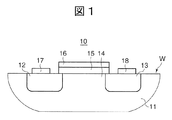
- FIG. 1 is a cross sectional view schematically showing a configuration of a MOSFET manufactured by a method for manufacturing a semiconductor device according to a first embodiment of the present invention.
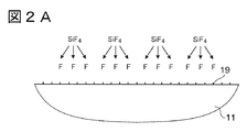
- FIGS. 2A to 2C are process diagrams showing a gate insulating film forming process as a method of manufacturing a semiconductor device according to the present embodiment.
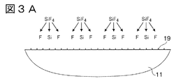
- FIGS. 3A to 3D are process diagrams showing a formation process of a gate insulating film as a method for manufacturing a semiconductor device according to a second embodiment of the present invention.
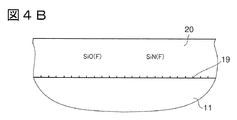
- FIGS. 4A to 4C FIGS.
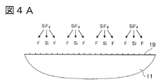
- FIGS. 4A to 4C are process diagrams showing a gate insulating film forming process as a method of manufacturing a semiconductor device according to a third embodiment of the present invention.
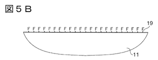
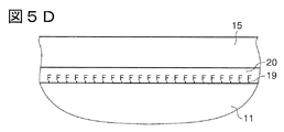
- FIGS. 5A to 5D are process diagrams showing a first modification of the gate insulating film forming process of FIGS. 2A to 2C.
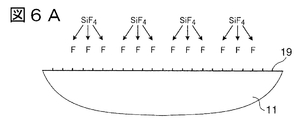
- FIGS. 6A to 6E are process diagrams showing a second modification of the gate insulating film forming process of FIGS. 2A to 2C.
- FIG. 1 is a cross-sectional view schematically showing the configuration of a MOSFET (metal oxide semiconductor effect transistor) manufactured by the method for manufacturing a semiconductor device according to the present embodiment.
- MOSFET metal oxide semiconductor effect transistor
- MOSFET 10 includes a silicon carbide base portion 11 constituted by a part of a wafer W made of silicon carbide, a drain region 12, a source region 13, and a drain region that are formed apart from each other on the surface layer of silicon carbide base portion 11.
- a drain electrode 17 and a source electrode 18 are formed on the source region 13, respectively.
- the mobility of the channel region 14 may be low because a dangling bond of silicon carbide exists at the interface between the gate insulating film 15 and the channel region 14 and the interface state density is high.
- the dangling bonds of silicon carbide are terminated by a gate insulating film formation process of FIGS. 2A to 2C described later.
- FIGS. 2A to 2C are process diagrams showing a gate insulating film forming process as a method of manufacturing a semiconductor device according to the present embodiment.
- 2A to 2C the termination of the dangling bonds 19 and the gate insulating film 15 in the silicon carbide base 11 are formed.
- the silicon carbide dangling bonds 19 are exaggerated for easy understanding.
- the surface layer of the silicon carbide base 11 on the wafer W is exposed to a halogen atmosphere from which air is excluded (FIG. 2A).
- a halogen atmosphere from which air is excluded
- F fluorine
- a processing gas for example, silicon tetrafluoride (SiF 4 ) gas.
- the halogen atmosphere and the temperature of the wafer W are maintained at room temperature, for example, 25 ° C. ⁇ 10 ° C.
- halogens such as fluorine are highly reactive, when the silicon carbide base 11 is exposed to a halogen atmosphere containing dissociated fluorine, the fluorine positively bonds the dangling bonds 19 of the silicon carbide base 11 and each unbonded bond. Hand 19 is terminated with fluorine (FIG. 2B).
- the gate insulating film 15 made of, for example, an oxide film, a nitride film, or another dielectric film is formed on the surface layer of the silicon carbide base 11 without exposing each dangling bond 19 terminated with fluorine to the atmosphere. Then, this process ends (FIG. 2C). Note that this process differs from the gate insulating film forming process of FIGS. 3A to 3D described later, and the gate insulating film 15 corresponding to the silicon oxide / silicon nitride film 20 described later is simultaneously formed with the termination of each dangling bond 19 by fluorine. None formed.
- the surface layer of the silicon carbide base portion 11 is exposed to a halogen atmosphere. Since the halogen is highly reactive, each dangling bond 19 must be terminated sufficiently. It is possible to reduce the interface state density of the surface layer of the silicon carbide base 11 and sufficiently improve the mobility of the channel region 14.
- the temperature of the halogen atmosphere is maintained at, for example, 25 ° C. ⁇ 10 ° C.
- the plasma dissociates the halogen from the processing gas. Therefore, it is possible to eliminate the need for the halogen atmosphere or the temperature of the wafer W to be high.
- the halogen atmosphere is set to a high temperature, etching occurs in the silicon carbide wafer.
- the gate insulating film forming process in FIGS. 2A to 2C is a low temperature process, the etching of the silicon carbide wafer can be avoided.
- the gate insulating film formation process in FIGS. 2A to 2C is an exposure process to a low-temperature halogen atmosphere, the mobility of the channel region 14 can be improved.
- the low temperature in this embodiment is 0 ° C. to 200 ° C., preferably 0 ° C. to 150 ° C.
- silicon tetrafluoride gas is used as the halogen supply source gas.
- any gas containing halogen can be used as the halogen supply source gas.
- a fluorine (F 2 ) gas or a gas containing a halogen other than fluorine, for example, silicon tetrachloride (SiCl 4 ) gas or chlorine (Cl 2 ) gas containing chlorine may be used. Since halogens other than fluorine are also highly reactive, each dangling bond 19 can be terminated sufficiently.
- the temperature of the halogen atmosphere is maintained at, for example, 25 ° C. ⁇ 10 ° C., but the halogen atmosphere and the wafer W are kept at a high temperature, for example, 600 ° C. or more. Preferably, it may be maintained at 900 ° C. or higher, more preferably 1000 ° C. to 1300 ° C.
- the halogen is dissociated from the halogen supply gas by heat, it is possible to eliminate the need for plasma to exist in the halogen atmosphere.
- the configuration of the processing apparatus that terminates each dangling bond 19 can be simplified. it can.
- the halogen supply gas is fluorine gas or chlorine gas
- the energy of fluorine and chlorine dissociated from the fluorine gas and chlorine gas becomes too high.
- Etching of the surface layer of the silicon carbide base portion 11 with fluorine or chlorine becomes more dominant than the end of 19, and the surface layer of the silicon carbide base portion 11 becomes rough, and the interface state density cannot be reduced. Therefore, when fluorine gas or chlorine gas is used as the halogen supply gas, it is preferable to dissociate fluorine or chlorine from fluorine gas or chlorine gas by maintaining plasma in the halogen atmosphere without maintaining the halogen atmosphere at a high temperature. .
- 3A to 3D are process diagrams showing a gate insulating film formation process as a method for manufacturing a semiconductor device according to the present embodiment.
- the halogen atmosphere to which the surface layer of the silicon carbide base portion 11 on the wafer W is exposed is decompressed and plasma is generated, so that a processing gas containing halogen, for example, silicon tetrafluoride gas, oxygen (O 2 as an oxygen supply source gas) is used.
- a processing gas containing halogen for example, silicon tetrafluoride gas, oxygen (O 2 as an oxygen supply source gas) is used.
- a processing gas containing halogen for example, silicon tetrafluoride gas, oxygen (O 2 as an oxygen supply source gas
- O 2 oxygen
- NH 3 ammonia
- silicon oxide (SiO) / silicon nitride (SiN) film 20 (another insulating film) having a film thickness of, for example, 3 nm to 30 nm on the surface layer of the silicon carbide base 11 (FIG. 3B).
- SiO silicon oxide
- SiN silicon nitride
- the silicon dissociated from the silicon tetrafluoride gas is not completely separated from the fluorine when the silicon oxide / silicon nitride film 20 is formed.
- the silicon oxide / silicon nitride film 20 contains Si—F bonds, and as a result, the silicon oxide / silicon nitride film 20 contains fluorine.
- this process differs from the above-described gate insulating film formation process of FIGS. 2A to 2C, and that the Si—F bond is mixed into the silicon oxide / silicon nitride film 20 for termination of each dangling bond 19 by fluorine. At the same time, it can be said that the silicon oxide / silicon nitride film 20 which functions as a part of the gate insulating film is formed.
- a plasma treatment is performed to bring the silicon oxide / silicon nitride film 20 into contact with plasma.
- high energy is applied to the fluorine contained in the silicon oxide / silicon nitride film 20 from the plasma, the Si—F bond derived from the silicon tetrafluoride gas is broken, and the fluorine freely passes through the silicon oxide / silicon nitride film 20.
- a part of the fluorine that freely moves reaches each dangling bond 19 on the surface layer of the silicon carbide base 11, and bonds with each dangling bond 19 to terminate each dangling bond 19.
- excess fluorine that has not been bonded to each dangling bond 19 remains high in energy, and thus desorbs from the silicon oxide / silicon nitride film 20 (FIG. 3C).
- an additional gate insulating film 15 made of, for example, an oxide film, a nitride film, or another dielectric film is formed on the silicon oxide / silicon nitride film 20 (FIG. 3D), and this process is terminated.
- the silicon oxide / silicon nitride film 20 from which fluorine has been eliminated may also constitute a part of the gate insulating film 15, and the thickness of the gate insulating film 15 does not have to be a specific value. It is preferable that the electrical characteristics required for the insulating film 15 and the silicon oxide / silicon nitride film 20 be realized.
- the film thickness of the formed silicon oxide / silicon nitride film 20 is as small as 3 nm to 30 nm, for example, it is included in the silicon oxide / silicon nitride film 20.
- the amount of fluorine can be reduced, so that fluorine can be prevented from remaining in the silicon oxide / silicon nitride film 20.
- the silicon oxide / silicon nitride film 20 is subjected to plasma treatment.
- the silicon oxide / silicon nitride film 20 is not subjected to plasma treatment, and silicon oxide / nitride is not subjected to plasma treatment.
- the silicon film 20 may be heat-treated with a heater or the like at a high temperature, for example, 600 ° C. or higher, preferably 900 ° C. or higher, more preferably 1000 ° C. to 1300 ° C.
- the silicon oxide / silicon nitride film 20 is formed using silicon tetrafluoride gas.
- a gas containing silicon can be used instead of the silicon tetrafluoride gas.
- the silicon oxide / silicon nitride film 20 may be formed using a silicon tetrachloride gas. In this case, the silicon oxide / silicon nitride film 20 contains chlorine, and each dangling bond 19 is terminated with chlorine.
- the silicon oxide / silicon nitride film 20 when the silicon oxide / silicon nitride film 20 is formed by CVD, not only the oxygen supply source gas but also the nitrogen supply source gas is supplied to the halogen atmosphere. Only the source gas may be supplied, or only the nitrogen source gas may be supplied. In this case, only the silicon oxide film containing halogen (fluorine) or only the silicon nitride film is formed on the surface layer of the silicon carbide base portion 11.
- FIGS. 4A to 4C are process diagrams showing a gate insulating film forming process as a method for manufacturing a semiconductor device according to the present embodiment.
- the halogen atmosphere to which the surface layer of the silicon carbide base 11 is exposed is decompressed and plasma is generated, for example, silicon tetrafluoride gas, oxygen gas, Further, nitrogen gas or ammonia gas is dissociated by plasma (FIG. 4A), and a silicon oxide / silicon nitride film 20 having a film thickness of, for example, 40 nm to 50 nm is formed on the surface layer of the silicon carbide base 11 by CVD (FIG. 4). 4B).
- plasma for example, silicon tetrafluoride gas, oxygen gas, Further, nitrogen gas or ammonia gas is dissociated by plasma (FIG. 4A), and a silicon oxide / silicon nitride film 20 having a film thickness of, for example, 40 nm to 50 nm is formed on the surface layer of the silicon carbide base 11 by CVD (FIG. 4). 4B).
- plasma treatment is performed to bring the silicon oxide / silicon nitride film 20 into contact with the plasma, and each dangling bond 19 is terminated by fluorine, while excess fluorine is desorbed from the silicon oxide / silicon nitride film 20,
- An additional gate insulating film 15 made of an oxide film, a nitride film, or another dielectric film is formed (FIG. 4C), and this process is terminated.
- a silicon oxide / silicon nitride film 20 containing fluorine having a thickness of 40 nm to 50 nm is formed.
- the gate insulating film 15 is formed by using a material other than the silicon oxide / silicon nitride film 20. The need to form an insulating film can be eliminated, and the throughput of forming the gate insulating film 15 can be improved.
- the silicon oxide / silicon nitride film 20 is also subjected to plasma treatment.
- the silicon film 20 may be heat-treated with a heater or the like at a high temperature, for example, 600 ° C. or higher, preferably 900 ° C. or higher, more preferably 1000 ° C. to 1300 ° C.
- a heater or the like at a high temperature, for example, 600 ° C. or higher, preferably 900 ° C. or higher, more preferably 1000 ° C. to 1300 ° C.
- the fluorine moves freely in the silicon oxide / silicon nitride film 20 and is bonded to each dangling bond 19.
- Each dangling bond 19 is terminated while excess fluorine is desorbed from the silicon oxide / silicon nitride film 20.
- the gate insulating film 15 may be formed in a chamber different from the chamber in which the surface layer of the silicon carbide base 11 is exposed to a halogen atmosphere.
- the interface of the channel region 14 may be roughened, such as a natural oxide film formed on the surface layer of the silicon carbide base 11 by a small amount of air or the like entering the transfer path. There is sex.
- the surface layer of the silicon carbide base 11 is exposed to a halogen atmosphere containing fluorine dissociated from silicon tetrafluoride (FIG. 5A), and each unbonded hand 19 is exposed.
- a halogen atmosphere containing fluorine dissociated from silicon tetrafluoride FIGS. 5A to 5D
- the silicon oxide / nitridation functioning as a part of the gate insulating film by CVD or the like on the surface layer of the silicon carbide base 11 of the wafer W
- a silicon film 20 is formed (FIG. 5C), and then an additional gate insulating film 15 made of an oxide film, a nitride film, or another dielectric film is formed on the silicon oxide / silicon nitride film 20 in another chamber. Good (FIG. 5D).
- the silicon oxide / silicon nitride film 20 formed in FIG. 5C also functions as a cap layer for the surface layer of the silicon carbide base 11, and a small amount of air that has entered the transport path and the unbonded hands 19 are terminated with fluorine. Further, contact with the surface layer of the silicon carbide base portion 11 is prevented, and a natural oxide film is prevented from being formed on the surface layer of the silicon carbide base portion 11.
- the silicon oxide / silicon nitride film 20 does not contain fluorine. There is no need to desorb fluorine from the silicon / silicon nitride film 20, and whether or not the silicon oxide / silicon nitride film 20 is subjected to plasma treatment or heat treatment may be any. There is no particular restriction on the timing of performing the plasma treatment or the heat treatment. For example, the heat treatment for phosphorus diffusion of gate polysilicon performed later in the semiconductor device manufacturing process may be used in combination with the heat treatment of the silicon oxide / silicon nitride film 20. Good.
- the silicon oxide / silicon nitride film 20 contains fluorine (FIGS. 6A to 6C).
- Plasma treatment or heat treatment is applied to the silicon oxide / silicon nitride film 20 to impart high energy to fluorine, and excess fluorine contained in the silicon oxide / silicon nitride film 20 is desorbed (FIG. 6D).
- the silicon oxide / silicon nitride film 20 is not only part of the gate insulating film but also the surface layer of the silicon carbide base 11 by CVD.
- the CVD only the oxygen source gas or only the nitrogen source gas is supplied in the CVD, and only the silicon oxide film or silicon nitride is used as the surface cap layer of the silicon carbide base 11. Only a film may be formed.
- Another object of the present invention is to supply a storage medium storing software program codes for realizing the functions of the above-described embodiments to a control unit of a computer, for example, a semiconductor device manufacturing apparatus, and store it in the CPU of the control unit. It is also achieved by reading and executing the program code stored on the medium.
- the program code itself read from the storage medium realizes the functions of the above-described embodiment, and the program code and the storage medium storing the program code constitute the present invention.
- Examples of the storage medium for supplying the program code include RAM, NV-RAM, floppy (registered trademark) disk, hard disk, magneto-optical disk, CD-ROM, CD-R, CD-RW, DVD (DVD). -ROM, DVD-RAM, DVD-RW, DVD + RW) and other optical disks, magnetic tapes, non-volatile memory cards, other ROMs, etc., as long as they can store the program code.
- the program code may be supplied to the control unit by downloading from another computer or database (not shown) connected to the Internet, a commercial network, a local area network, or the like.
- the program code read from the storage medium is written in the memory provided in the function expansion board inserted in the control unit or the function expansion unit connected to the control unit, the program code is read based on the instruction of the program code.
- the CPU of the function expansion board or the function expansion unit performs part or all of the actual processing and the functions of the above-described embodiments are realized by the processing is also included.
- the form of the program code may be in the form of object code, program code executed by an interpreter, script data supplied to the OS, and the like.
Landscapes
- Insulated Gate Type Field-Effect Transistor (AREA)
- Formation Of Insulating Films (AREA)
Abstract
チャネルの移動度を十分に改善することができる半導体デバイスの製造方法を提供する。ウエハWにおける炭化硅素基部11の表層を、四フッ化硅素ガスからプラズマによって解離したフッ素を含むハロゲン雰囲気に暴露し、該暴露された表層の上にゲート絶縁膜15を形成する。
Description
本発明は、炭化硅素からなる基板に形成される絶縁膜を含む半導体デバイス及びその製造方法に関する。
炭化硅素(SiC)はバンドギャップが約3eVであり、半導体材料として用いることができるが、絶縁破壊電圧がシリコン(Si)の10倍もある耐性の高い半導体材料であるため、大電流が流れるトランジスタ構造を有する宇宙用デバイスやパワーデバイス等の半導体デバイスに用いることが検討されている。
上述した半導体デバイスは炭化硅素のウエハから製造されるが、ウエハの表面にゲート絶縁膜を形成することによって当該ゲート絶縁膜で覆われた箇所をチャネルとして機能させる場合、ゲート絶縁膜とチャネルの界面には炭化硅素の未結合手(ダングリングボンド)が存在するため、界面準位密度が高くなってチャネルの移動度が低下する。
そこで、未結合手を窒素(N)、リン(P)や水素(H)で終端させて界面準位密度を低下させることが提案されている(例えば、非特許文献1参照。)。
D.Okamoto,H.Yano,K.Hirata,T.Hatayama,and T.Fuyuki,″Improved Inversion Channel Mobility in 4H−SiC MOSFETs on Si−face Utilizing Phosphorus−Doped Gate Oxide″,IEEE Electron Device Lett.,Vol.31,No.7,pp.710−712(2010)
しかしながら、窒素、リンや水素は炭化硅素との反応性が高くないため、未結合手を充分に終端処理することができず、窒素、リンや水素によって終端処理を行っても、窒素、リンや水素で終端処理を行わない場合と比較して未結合手の終端度合に改善は見れるが、充分に界面準位密度を低減できない。また、窒素、リンや水素による未結合手の終端を促進するために、処理温度を、例えば、1000℃以上まで高くすると炭化硅素から炭素(C)が脱離することがある。このとき、炭素の脱離が進行することにより、炭素残留物が炭化硅素とゲート絶縁膜との界面及びゲート絶縁膜中に残存するため、窒素、リンや水素を用いてもチャネルの移動度は十分に改善されないか、若しくはゲート絶縁膜の特性を劣化させる場合がある。
本発明の目的は、チャネルの移動度を十分に改善することができる半導体デバイス及びその製造方法を提供することにある。
上記目的を達成するために、本発明によれば、炭化硅素からなる基板の表層をハロゲン雰囲気に暴露し、該暴露された表層の上に絶縁膜を形成する半導体デバイスの製造方法が提供される。
上記目的を達成するために、本発明によれば、炭化硅素からなる基板の表層の上にハロゲンを含有する絶縁膜を形成し、該絶縁膜へプラズマ処理を施す半導体デバイスの製造方法が提供される。
上記目的を達成するために、本発明によれば、炭化硅素からなる基板の表層の上にハロゲンを含有する絶縁膜を形成し、該絶縁膜へ熱処理を施す半導体デバイスの製造方法が提供される。
上記目的を達成するために、本発明によれば、炭化硅素からなる基板の表層の上に絶縁膜を形成された半導体デバイスであって、前記炭化硅素の未結合手がハロゲンで終端されている半導体デバイスが提供される。
本発明によれば、炭化硅素からなる基板の表層がハロゲン雰囲気に暴露される。ハロゲンは反応性が高いため、炭化珪素の未結合手を充分に終端することができ、よって、チャネルの移動度を十分に改善することができる。
[図1]本発明の第1の実施の形態に係る半導体デバイスの製造方法によって製造されるMOSFETの構成を概略的に示す断面図である。
[図2A乃至図2C]本実施の形態に係る半導体デバイスの製造方法としてのゲート絶縁膜の形成処理を示す工程図である。
[図3A乃至図3D]本発明の第2の実施の形態に係る半導体デバイスの製造方法としてのゲート絶縁膜の形成処理を示す工程図である。
[図4A乃至図4C]本発明の第3の実施の形態に係る半導体デバイスの製造方法としてのゲート絶縁膜の形成処理を示す工程図である。
[図5A乃至図5D]図2A乃至図2Cのゲート絶縁膜の形成処理の第1の変形例を示す工程図である。
[図6A乃至図6E]図2A乃至図2Cのゲート絶縁膜の形成処理の第2の変形例を示す工程図である。
[図2A乃至図2C]本実施の形態に係る半導体デバイスの製造方法としてのゲート絶縁膜の形成処理を示す工程図である。
[図3A乃至図3D]本発明の第2の実施の形態に係る半導体デバイスの製造方法としてのゲート絶縁膜の形成処理を示す工程図である。
[図4A乃至図4C]本発明の第3の実施の形態に係る半導体デバイスの製造方法としてのゲート絶縁膜の形成処理を示す工程図である。
[図5A乃至図5D]図2A乃至図2Cのゲート絶縁膜の形成処理の第1の変形例を示す工程図である。
[図6A乃至図6E]図2A乃至図2Cのゲート絶縁膜の形成処理の第2の変形例を示す工程図である。
以下、本発明の実施の形態について図面を参照しながら説明する。
まず、本発明の第1の実施の形態に係る半導体デバイスの製造方法について説明する。
図1は、本実施の形態に係る半導体デバイスの製造方法によって製造されるMOSFET(metal oxide semiconductor field effect transistor)の構成を概略的に示す断面図である。
図1において、MOSFET10は、炭化硅素からなるウエハWの一部によって構成される炭化硅素基部11と、炭化硅素基部11の表層において互いに離間して形成されるドレイン領域12、ソース領域13と、ドレイン領域12及びソース領域13に挟まれるチャネル領域14と、該チャネル領域14の上に形成されるゲート絶縁膜15と、該ゲート絶縁膜15の上に形成されるゲート電極16と、ドレイン領域12、ソース領域13の上にそれぞれ形成されるドレイン電極17、ソース電極18とを有する。
MOSFET10では、ゲート絶縁膜15とチャネル領域14の界面には炭化硅素の未結合手が存在し、界面準位密度が高いため、チャネル領域14の移動度が低いことがある。本実施の形態では、これに対応して、後述する図2A乃至図2Cのゲート絶縁膜の形成処理によって炭化硅素の未結合手を終端させる。
図2A乃至図2Cは、本実施の形態に係る半導体デバイスの製造方法としてのゲート絶縁膜の形成処理を示す工程図である。図2A乃至図2Cのゲート絶縁膜の形成処理では、炭化硅素基部11における未結合手19の終端及びゲート絶縁膜15の形成が行われる。なお、図2A乃至図2C以降の図面では、理解を容易にするために、炭化硅素の未結合手19を誇張して描画している。
まず、ウエハWにおける炭化硅素基部11の表層を、大気が排除されたハロゲン雰囲気に暴露する(図2A)。ハロゲン雰囲気ではプラズマが存在し、ハロゲン供給源ガスとしての処理ガス、例えば、四フッ化硅素(SiF4)ガスからプラズマによってフッ素(F)が解離している。また、ハロゲン雰囲気やウエハWの温度は、常温、例えば、25℃±10℃に維持されている。
フッ素等のハロゲンは反応性が高いため、解離したフッ素を含むハロゲン雰囲気に炭化硅素基部11が暴露されると、フッ素が炭化硅素基部11の未結合手19を積極的と結合し、各未結合手19はフッ素で終端される(図2B)。
次いで、フッ素で終端された各未結合手19を大気へ暴露させることなく、炭化硅素基部11の表層の上に、例えば、酸化膜、窒化膜や他の誘電膜からなるゲート絶縁膜15を形成し、本処理を終了する(図2C)。なお、本処理は後述する図3A乃至図3Dのゲート絶縁膜の形成処理と異なり、各未結合手19のフッ素による終端と同時に後述の酸化珪素/窒化珪素膜20に相当するゲート絶縁膜15が形成されることはない。
図2A乃至図2Cのゲート絶縁膜の形成処理によれば、炭化硅素基部11の表層がハロゲン雰囲気に暴露されるが、ハロゲンは反応性が高いため、各未結合手19を充分に終端することができ、炭化硅素基部11の表層の界面準位密度を低下させてチャネル領域14の移動度を十分に改善することができる。
また、図2A乃至図2Cのゲート絶縁膜の形成処理では、ハロゲン雰囲気の温度が、例えば、25℃±10℃に維持されるが、ハロゲン雰囲気ではプラズマが処理ガスからハロゲンを解離するので、ハロゲンを解離させるためにハロゲン雰囲気、若しくはウエハWを高温にする必要を無くすことができる。ハロゲン雰囲気を高温にした場合、炭化硅素のウエハにおいてエッチングが生じるが、図2A乃至図2Cのゲート絶縁膜の形成処理は低温処理であるため、炭化硅素のウエハのエッチングを回避することができる。また、高温処理の場合、フッ化と同時に残留酸素によって酸化が生じ、結果としてフッ素による未結合手の終端が充分に行われないため、移動度の改善度合が小さいという可能性があるが、図2A乃至図2Cのゲート絶縁膜の形成処理は低温のハロゲン雰囲気への暴露処理であるため、チャネル領域14の移動度を改善することができる。なお、本実施の形態における低温とは0℃~200℃、好ましくは0℃~150℃である。
上述した図2A乃至図2Cのゲート絶縁膜の形成処理では、ハロゲン供給源ガスとして四フッ化硅素ガスを用いたが、ハロゲンを含むガスであればハロゲン供給源ガスとして用いることができ、例えば、フッ素(F2)ガスやフッ素以外のハロゲンを含むガス、例えば、塩素を含む四塩化硅素(SiCl4)ガスや塩素(Cl2)ガスを用いてもよい。フッ素以外のハロゲンも反応性が高いため、各未結合手19を充分に終端することができる。
また、上述した図2A乃至図2Cのゲート絶縁膜の形成処理では、ハロゲン雰囲気の温度が、例えば、25℃±10℃に維持されるが、ハロゲン雰囲気やウエハWを高温、例えば、600℃以上、好ましくは900℃以上、より好ましくは1000℃~1300℃に維持してもよい。この場合、熱によってハロゲン供給源ガスからハロゲンが解離するので、ハロゲン雰囲気にプラズマを存在させる必要を無くすことができ、例えば、各未結合手19を終端させる処理装置の構成を簡素化することができる。但し、ハロゲン供給源ガスがフッ素ガスや塩素ガスのとき、ハロゲン雰囲気を高温に維持すると、フッ素ガスや塩素ガスから解離したフッ素や塩素のエネルギーが高くなりすぎるため、フッ素や塩素による各未結合手19の終端よりも、フッ素や塩素による炭化硅素基部11の表層のエッチングが優勢となり、炭化硅素基部11の表層が荒れて界面準位密度を低下させることができない。したがって、ハロゲン供給源ガスとしてフッ素ガスや塩素ガスを用いる場合は、ハロゲン雰囲気を高温に維持することなく、ハロゲン雰囲気にプラズマを存在させてフッ素ガスや塩素ガスからフッ素や塩素を解離させることが好ましい。
次に、本発明の第2の実施の形態に係る半導体デバイスの製造方法について説明する。
図3A乃至図3Dは、本実施の形態に係る半導体デバイスの製造方法としてのゲート絶縁膜の形成処理を示す工程図である。
まず、ウエハWにおける炭化硅素基部11の表層が暴露されるハロゲン雰囲気を減圧するとともにプラズマを発生させ、ハロゲンを含む処理ガス、例えば、四フッ化硅素ガス、酸素供給源ガスとしての酸素(O2)ガス、さらには、窒素供給源ガスとしての窒素(N2)ガスやアンモニア(NH3)ガスをハロゲン雰囲気へ供給し、これらのガスをプラズマによって解離させ(図3A)、CVD(Chemical Vapor Deposition)によって炭化硅素基部11の表層に、膜厚が、例えば、3nm~30nmの酸化珪素(SiO)/窒化珪素(SiN)膜20(他の絶縁膜)を形成する(図3B)。ここで、四フッ化硅素ガスにおけるSi−F結合の結合エネルギーは高いため、酸化珪素/窒化珪素膜20が形成される際、四フッ化硅素ガスから解離した硅素はフッ素と完全に分離せず、酸化珪素/窒化珪素膜20にはSi−F結合が含まれ、結果として、酸化珪素/窒化珪素膜20はフッ素を含む。なお、本処理は上述した図2A乃至図2Cのゲート絶縁膜の形成処理と異なり、各未結合手19のフッ素による終端のためのSi−F結合の酸化珪素/窒化珪素膜20への混入と同時に、ゲート絶縁膜の一部として機能する酸化珪素/窒化珪素膜20が形成されると言える。
次いで、酸化珪素/窒化珪素膜20へプラズマを接触させるプラズマ処理を施す。このとき、酸化珪素/窒化珪素膜20に含まれるフッ素にプラズマから高いエネルギーが付与され、四フッ化硅素ガス由来のSi−F結合が崩れてフッ素が酸化珪素/窒化珪素膜20内を自由に移動する。自由に移動する一部のフッ素は炭化硅素基部11の表層における各未結合手19へ到達し、各未結合手19と結合して各未結合手19を終端する。一方、各未結合手19と結合しなかった余剰のフッ素は付与されたエネルギーが高いままであるため、酸化珪素/窒化珪素膜20から脱離する(図3C)。
次いで、酸化珪素/窒化珪素膜20の上に、例えば、酸化膜、窒化膜や他の誘電膜からなる追加のゲート絶縁膜15を形成し(図3D)、本処理を終了する。なお、フッ素が脱離した酸化珪素/窒化珪素膜20もゲート絶縁膜15の一部を構成してもよく、ゲート絶縁膜15の厚さは特定の値である必要は無いが、MOSFET10においてゲート絶縁膜15及び酸化珪素/窒化珪素膜20に求められる電気的特性を実現可能な値であることが好ましい。
図3A乃至図3Dのゲート絶縁膜の形成処理によれば、炭化硅素基部11の表層をハロゲン雰囲気に暴露する際に、表層の上に酸化珪素/窒化珪素膜20が形成され、同時に四フッ化硅素ガスにおけるSi−F結合が酸化珪素/窒化珪素膜20へ混入される。このとき、Si−F結合の結合エネルギーが高いため、四フッ化硅素ガスから解離した硅素はフッ素と完全に分離せず、結果として形成される酸化珪素/窒化珪素膜20にはフッ素が含まれ、各未結合手19へフッ素を確実に供給することができ、もって、各未結合手19をフッ素で確実に終端することができる。
また、図3A乃至図3Dのゲート絶縁膜の形成処理では、形成された酸化珪素/窒化珪素膜20にプラズマ処理が施されるので、酸化珪素/窒化珪素膜20に含まれるフッ素へ高いエネルギーが付与されてフッ素による各未結合手19の終端が促進されるとともに、余剰のフッ素が酸化珪素/窒化珪素膜20から脱離する。その結果、フッ素を含まないゲート絶縁膜15を得ることができ、ゲート絶縁膜15の特性を改善することができる。
上述した図3A乃至図3Dのゲート絶縁膜の形成処理では、形成される酸化珪素/窒化珪素膜20の膜厚が、例えば、3nm~30nmと小さいので、酸化珪素/窒化珪素膜20に含まれるフッ素の量を少なくすることができ、もって、酸化珪素/窒化珪素膜20にフッ素が残存するのを防止することができる。
上述した図3A乃至図3Dのゲート絶縁膜の形成処理では、酸化珪素/窒化珪素膜20にプラズマ処理を施したが、酸化珪素/窒化珪素膜20にプラズマ処理を施すことなく、酸化珪素/窒化珪素膜20をヒータ等で高温、例えば、600℃以上、好ましくは900℃以上、より好ましくは1000℃~1300℃に熱して熱処理を施してもよい。このとき、酸化珪素/窒化珪素膜20に含まれるフッ素へ熱によって高いエネルギーが付与されるため、フッ素が酸化珪素/窒化珪素膜20内を自由に移動し、各未結合手19と結合して各未結合手19を終端する一方、余剰のフッ素は酸化珪素/窒化珪素膜20から脱離する。
図3A乃至図3Dのゲート絶縁膜の形成処理において、CVDによって酸化珪素/窒化珪素膜20を形成する際、四フッ化硅素ガスを用いて酸化珪素/窒化珪素膜20を形成したが、ハロゲンと硅素を含むガスであれば四フッ化硅素ガスの代わりに用いることができ、例えば、四塩化硅素ガスを用いて酸化珪素/窒化珪素膜20を形成してもよい。この場合、酸化珪素/窒化珪素膜20には塩素が含まれ、各未結合手19は塩素によって終端される。
なお、図3A乃至図3Dのゲート絶縁膜の形成処理では、CVDによって酸化珪素/窒化珪素膜20を形成する際、酸素供給源ガスだけでなく窒素供給源ガスをハロゲン雰囲気へ供給したが、酸素供給源ガスのみを供給してもよく、若しくは窒素供給源ガスのみを供給してもよい。この場合、炭化硅素基部11の表層にハロゲン(フッ素)を含む酸化珪素膜のみ、若しくは窒化珪素膜のみが形成される。
次に、本発明の第3の実施の形態に係る半導体デバイスの製造方法について説明する。
図4A乃至図4Cは、本実施の形態に係る半導体デバイスの製造方法としてのゲート絶縁膜の形成処理を示す工程図である。
まず、図3A乃至図3Dのゲート絶縁膜の形成処理と同様に、炭化硅素基部11の表層が暴露されるハロゲン雰囲気を減圧するとともにプラズマを発生させ、例えば、四フッ化硅素ガス、酸素ガス、さらには、窒素ガスやアンモニアガスをプラズマによって解離させ(図4A)、CVDによって炭化硅素基部11の表層に、膜厚が、例えば、40nm~50nmの酸化珪素/窒化珪素膜20を形成する(図4B)。このときも、図3A乃至図3Dのゲート絶縁膜の形成処理と同様に、各未結合手19のフッ素による終端のためのSi−F結合の酸化珪素/窒化珪素膜20への混入と同時に、ゲート絶縁膜の一部として機能する酸化珪素/窒化珪素膜20が形成され、結果として酸化珪素/窒化珪素膜20はフッ素を含む。
次いで、酸化珪素/窒化珪素膜20へプラズマを接触させるプラズマ処理を施し、フッ素によって各未結合手19を終端する一方、余剰のフッ素を酸化珪素/窒化珪素膜20から脱離させ、その上に酸化膜、窒化膜や他の誘電膜からなる追加のゲート絶縁膜15を形成し(図4C)、本処理を終了する。
図4A乃至図4Cのゲート絶縁膜の形成処理によれば、フッ素によって各未結合手19を終端する際、膜厚が40nm~50nmのフッ素を含む酸化珪素/窒化珪素膜20を形成し、さらに、酸化珪素/窒化珪素膜20へプラズマ処理を施して余剰のフッ素を脱離させてゲート絶縁膜15を形成するため、ゲート絶縁膜15を形成するために、酸化珪素/窒化珪素膜20以外の絶縁膜を形成する必要を無くすことができ、ゲート絶縁膜15の形成のスループットを向上することができる。
上述した図4A乃至図4Cのゲート絶縁膜の形成処理でも、酸化珪素/窒化珪素膜20にプラズマ処理を施したが、酸化珪素/窒化珪素膜20にプラズマ処理を施すことなく、酸化珪素/窒化珪素膜20をヒータ等で高温、例えば、600℃以上、好ましくは900℃以上、より好ましくは1000℃~1300℃に熱して熱処理を施してもよい。このときも、酸化珪素/窒化珪素膜20に含まれるフッ素へ熱によって高いエネルギーが付与されるため、フッ素が酸化珪素/窒化珪素膜20内を自由に移動し、各未結合手19と結合して各未結合手19を終端する一方、余剰のフッ素は酸化珪素/窒化珪素膜20から脱離する。
以上、本発明について、上記各実施の形態を用いて説明したが、本発明は上記各実施の形態に限定されるものではない。
例えば、図2A乃至図2Cのゲート絶縁膜の形成処理において、炭化硅素基部11の表層をハロゲン雰囲気に暴露するチャンバとは別のチャンバでゲート絶縁膜15を形成する場合がある。この場合、ウエハWを別のチャンバへ搬送する際に、搬送路内へ進入した微量の大気等によって炭化硅素基部11の表層に自然酸化膜が形成される等、チャネル領域14の界面が荒れる可能性がある。
これに対応して、図5A乃至図5Dに示すように、炭化硅素基部11の表層を、四フッ化硅素から解離したフッ素を含むハロゲン雰囲気に暴露し(図5A)、各未結合手19をフッ素で終端した(図5B)後、ウエハWを別のチャンバへ搬送する前に、ウエハWの炭化硅素基部11の表層の上にCVD等によってゲート絶縁膜の一部として機能する酸化珪素/窒化珪素膜20を形成し(図5C)、その後、別のチャンバで酸化珪素/窒化珪素膜20の上に酸化膜、窒化膜や他の誘電膜からなる追加のゲート絶縁膜15を形成してもよい(図5D)。
図5Cにおいて形成された酸化珪素/窒化珪素膜20は炭化硅素基部11の表層のキャップ層としても機能し、搬送路内へ進入した微量の大気等と、各未結合手19がフッ素で終端された炭化硅素基部11の表層とが接触するのを防止して炭化硅素基部11の表層に自然酸化膜が形成されるのを防止する。
特に、各未結合手19の終端後の酸化珪素/窒化珪素膜20の形成においてシラン(SiH4)ガスが用いられた場合、酸化珪素/窒化珪素膜20にはフッ素が含まれないため、酸化珪素/窒化珪素膜20からフッ素を脱離させる必要がなく、酸化珪素/窒化珪素膜20へプラズマ処理や熱処理を施すか否かはいずれでもよく、プラズマ処理や熱処理を施す場合であっても、プラズマ処理や熱処理を施すタイミングに特に制約は無く、例えば、半導体デバイスの製造工程において後に行われるゲートポリシリコンのリン拡散のための熱処理を、酸化珪素/窒化珪素膜20の熱処理に併用してもよい。
一方、各未結合手19の終端後の酸化珪素/窒化珪素膜20の形成において四フッ化硅素ガスが用いられた場合、酸化珪素/窒化珪素膜20はフッ素を含むため(図6A~図6C)、酸化珪素/窒化珪素膜20にプラズマ処理又は熱処理を施してフッ素へ高いエネルギーを付与し、酸化珪素/窒化珪素膜20に含まれる余剰のフッ素を脱離し(図6D)、その後、ゲート絶縁膜の一部として機能する酸化珪素/窒化珪素膜20の上に酸化膜、窒化膜や他の誘電膜からなる追加のゲート絶縁膜15を形成するのが好ましい(図6E))。このとき、プラズマ処理や熱処理によって高いエネルギーが付与されたフッ素の一部は酸化珪素/窒化珪素膜20から脱離することなく、炭化硅素基部11と酸化珪素/窒化珪素膜20の界面に到達し、終端されていない未結合手19が存在すれば、当該未結合手19を終端する。これにより、全ての未結合手19を確実に終端することができる。
なお、上述した図5A乃至図5Dや図6A乃至図6Eのゲート絶縁膜の形成処理では、CVDによって酸化珪素/窒化珪素膜20がゲート絶縁膜の一部としてだけではなく炭化硅素基部11の表層のキャップ層としても機能するように形成されたが、CVDにおいて酸素供給源ガスのみ、若しくは窒素供給源ガスのみを供給し、炭化硅素基部11の表層のキャップ層として酸化珪素膜のみ、若しくは窒化珪素膜のみを形成してもよい。
また、本発明の目的は、上述した実施の形態の機能を実現するソフトウェアのプログラムコードを記録した記憶媒体を、コンピュータ、例えば、半導体デバイス製造装置の制御部に供給し、制御部のCPUが記憶媒体に格納されたプログラムコードを読み出して実行することによっても達成される。
この場合、記憶媒体から読み出されたプログラムコード自体が上述した実施の形態の機能を実現することになり、プログラムコード及びそのプログラムコードを記憶した記憶媒体は本発明を構成することになる。
また、プログラムコードを供給するための記憶媒体としては、例えば、RAM、NV−RAM、フロッピー(登録商標)ディスク、ハードディスク、光磁気ディスク、CD−ROM、CD−R、CD−RW、DVD(DVD−ROM、DVD−RAM、DVD−RW、DVD+RW)等の光ディスク、磁気テープ、不揮発性のメモリカード、他のROM等の上記プログラムコードを記憶できるものであればよい。或いは、上記プログラムコードは、インターネット、商用ネットワーク、若しくはローカルエリアネットワーク等に接続される不図示の他のコンピュータやデータベース等からダウンロードすることにより制御部に供給されてもよい。
また、制御部が読み出したプログラムコードを実行することにより、上記実施の形態の機能が実現されるだけでなく、そのプログラムコードの指示に基づき、CPU上で稼動しているOS(オペレーティングシステム)等が実際の処理の一部又は全部を行い、その処理によって上述した実施の形態の機能が実現される場合も含まれる。
さらに、記憶媒体から読み出されたプログラムコードが、制御部に挿入された機能拡張ボードや制御部に接続された機能拡張ユニットに備わるメモリに書き込まれた後、そのプログラムコードの指示に基づき、その機能拡張ボードや機能拡張ユニットに備わるCPU等が実際の処理の一部又は全部を行い、その処理によって上述した実施の形態の機能が実現される場合も含まれる。
上記プログラムコードの形態は、オブジェクトコード、インタプリタにより実行されるプログラムコード、OSに供給されるスクリプトデータ等の形態から成ってもよい。
本出願は、2014年7月2日に出願された日本出願第2014−136918号に基づく優先権を主張するものであり、当該日本出願に記載された全内容を本出願に援用する。
W ウエハ
11 炭化硅素基部
15 ゲート絶縁膜
19 未結合手
20 酸化珪素/窒化珪素膜
11 炭化硅素基部
15 ゲート絶縁膜
19 未結合手
20 酸化珪素/窒化珪素膜
Claims (19)
- 炭化硅素からなる基板の表層をハロゲン雰囲気に暴露し、該暴露された表層の上に絶縁膜を形成することを特徴とする半導体デバイスの製造方法。
- 前記ハロゲン雰囲気では処理ガスからプラズマによってハロゲンが解離することを特徴とする請求項1記載の半導体デバイスの製造方法。
- 前記表層を前記ハロゲン雰囲気に暴露する際に、前記表層の上に酸化珪素膜及び窒化珪素膜の少なくとも1つからなる他の絶縁膜を形成することを特徴とする請求項1記載の半導体デバイスの製造方法。
- 前記形成された他の絶縁膜にプラズマ処理を施すことを特徴とする請求項3記載の半導体デバイスの製造方法。
- 前記形成された他の絶縁膜に熱処理を施すことを特徴とする請求項3記載の半導体デバイスの製造方法。
- 前記絶縁膜は前記形成された他の絶縁膜の上に形成されることを特徴とする請求項3乃至5のいずれか1項に記載の半導体デバイスの製造方法。
- 前記表層を前記ハロゲン雰囲気に暴露する際に、前記ハロゲン雰囲気、若しくは前記基板が高温に維持されることを特徴とする請求項1記載の半導体デバイスの製造方法。
- 前記ハロゲン雰囲気は600℃以上の温度に維持されることを特徴とする請求項7記載の半導体デバイスの製造方法。
- 前記表層が前記ハロゲン雰囲気に暴露された後に、該暴露された表層の上に酸化珪素膜及び窒化珪素膜の少なくとも1つを形成することを特徴とする請求項1記載の半導体デバイスの製造方法。
- 前記酸化珪素膜及び窒化珪素膜の少なくとも1つを形成する際にシラン(SiH4)が用いられることを特徴とする請求項9記載の半導体デバイスの製造方法。
- 前記酸化珪素膜及び窒化珪素膜の少なくとも1つを形成する際に四フッ化硅素(SiF4)が用いられることを特徴とする請求項9記載の半導体デバイスの製造方法。
- 前記四フッ化硅素を用いて形成された前記酸化珪素膜及び窒化珪素膜の少なくとも1つに熱処理を施すことを特徴とする請求項11記載の半導体デバイスの製造方法。
- 前記ハロゲン雰囲気に含まれるハロゲンはフッ素であることを特徴とする請求項1乃至12のいずれか1項に記載の半導体デバイスの製造方法。
- 前記ハロゲン雰囲気に含まれるハロゲンは塩素であることを特徴とする請求項1乃至12のいずれか1項に記載の半導体デバイスの製造方法。
- 炭化硅素からなる基板の表層の上にハロゲンを含有する絶縁膜を形成し、該絶縁膜へプラズマ処理を施すことを特徴とする半導体デバイスの製造方法。
- 炭化硅素からなる基板の表層の上にハロゲンを含有する絶縁膜を形成し、該絶縁膜へ熱処理を施すことを特徴とする半導体デバイスの製造方法。
- 炭化硅素からなる基板の表層の上に絶縁膜を形成された半導体デバイスであって、
前記炭化硅素の未結合手がハロゲンで終端されていることを特徴とする半導体デバイス。 - 前記ハロゲンはフッ素であることを特徴とする請求項17記載の半導体デバイス。
- 前記ハロゲンは塩素であることを特徴とする請求項17記載の半導体デバイス。
Applications Claiming Priority (2)
| Application Number | Priority Date | Filing Date | Title |
|---|---|---|---|
| JP2014136918A JP2016015407A (ja) | 2014-07-02 | 2014-07-02 | 半導体デバイス及びその製造方法 |
| JP2014-136918 | 2014-07-02 |
Publications (1)
| Publication Number | Publication Date |
|---|---|
| WO2016002916A1 true WO2016002916A1 (ja) | 2016-01-07 |
Family
ID=55019442
Family Applications (1)
| Application Number | Title | Priority Date | Filing Date |
|---|---|---|---|
| PCT/JP2015/069217 Ceased WO2016002916A1 (ja) | 2014-07-02 | 2015-06-26 | 半導体デバイス及びその製造方法 |
Country Status (2)
| Country | Link |
|---|---|
| JP (1) | JP2016015407A (ja) |
| WO (1) | WO2016002916A1 (ja) |
Families Citing this family (2)
| Publication number | Priority date | Publication date | Assignee | Title |
|---|---|---|---|---|
| JP6780414B2 (ja) * | 2016-09-29 | 2020-11-04 | 富士電機株式会社 | 炭化珪素半導体装置および炭化珪素半導体装置の製造方法 |
| JP7076971B2 (ja) * | 2017-09-28 | 2022-05-30 | キヤノン株式会社 | 撮像装置およびその製造方法ならびに機器 |
Citations (4)
| Publication number | Priority date | Publication date | Assignee | Title |
|---|---|---|---|---|
| US5840610A (en) * | 1997-01-16 | 1998-11-24 | Advanced Micro Devices, Inc. | Enhanced oxynitride gate dielectrics using NF3 gas |
| JP2008004680A (ja) * | 2006-06-21 | 2008-01-10 | Nissan Motor Co Ltd | 半導体装置及び半導体装置の製造方法 |
| JP2010206094A (ja) * | 2009-03-05 | 2010-09-16 | Elpida Memory Inc | 半導体装置及びその製造方法 |
| JP2012164788A (ja) * | 2011-02-07 | 2012-08-30 | Toshiba Corp | 半導体素子及びその製造方法 |
-
2014
- 2014-07-02 JP JP2014136918A patent/JP2016015407A/ja active Pending
-
2015
- 2015-06-26 WO PCT/JP2015/069217 patent/WO2016002916A1/ja not_active Ceased
Patent Citations (4)
| Publication number | Priority date | Publication date | Assignee | Title |
|---|---|---|---|---|
| US5840610A (en) * | 1997-01-16 | 1998-11-24 | Advanced Micro Devices, Inc. | Enhanced oxynitride gate dielectrics using NF3 gas |
| JP2008004680A (ja) * | 2006-06-21 | 2008-01-10 | Nissan Motor Co Ltd | 半導体装置及び半導体装置の製造方法 |
| JP2010206094A (ja) * | 2009-03-05 | 2010-09-16 | Elpida Memory Inc | 半導体装置及びその製造方法 |
| JP2012164788A (ja) * | 2011-02-07 | 2012-08-30 | Toshiba Corp | 半導体素子及びその製造方法 |
Also Published As
| Publication number | Publication date |
|---|---|
| JP2016015407A (ja) | 2016-01-28 |
Similar Documents
| Publication | Publication Date | Title |
|---|---|---|
| JP4813778B2 (ja) | 半導体装置 | |
| JPH11121453A (ja) | 半導体装置を形成する方法 | |
| CN1312737C (zh) | 制作栅极介电层的方法 | |
| US20130234163A1 (en) | Silicon carbide semiconductor device | |
| CN101208782A (zh) | 用于等离子氮化栅极介电层的氮化后二阶段退火的方法 | |
| JP2005353999A (ja) | 半導体装置およびその製造方法 | |
| JP2009272348A (ja) | 半導体装置およびその製造方法 | |
| JP2008283182A (ja) | Pmosトランジスタ製造方法及びcmosトランジスタ製造方法 | |
| CN107104144B (zh) | 半导体装置及其制造方法 | |
| WO2015015672A1 (ja) | 炭化珪素半導体装置及びその製造方法 | |
| WO2016002916A1 (ja) | 半導体デバイス及びその製造方法 | |
| JPH11274489A (ja) | 電界効果トランジスタ及びその製造方法 | |
| JP5166136B2 (ja) | 半導体装置のゲート酸化膜上に窒化珪素層を形成し、窒化物層を熱処理する方法 | |
| US20120261763A1 (en) | Semiconductor Structure and Method for Manufacturing the Same | |
| JP6174756B2 (ja) | Soi基板の製造方法 | |
| JP2015142078A (ja) | 炭化ケイ素半導体装置およびその製造方法 | |
| KR100788361B1 (ko) | 모스펫 소자의 형성 방법 | |
| CN104051506B (zh) | 氟掺杂信道硅锗层 | |
| JP4867333B2 (ja) | 炭化珪素半導体装置、及び炭化珪素半導体装置の製造方法 | |
| JP2830828B2 (ja) | 半導体装置の製造方法 | |
| JP2010103296A (ja) | 酸化ゲルマニウムの製造方法およびそれを用いた半導体デバイスの製造方法 | |
| JP3826792B2 (ja) | 半導体装置の製造方法 | |
| JPH03129774A (ja) | 半導体装置及びその製造方法 | |
| JP3372030B2 (ja) | 薄膜絶縁膜の形成方法 | |
| JP2013157425A (ja) | 半導体装置の製造方法 |
Legal Events
| Date | Code | Title | Description |
|---|---|---|---|
| 121 | Ep: the epo has been informed by wipo that ep was designated in this application |
Ref document number: 15815093 Country of ref document: EP Kind code of ref document: A1 |
|
| NENP | Non-entry into the national phase |
Ref country code: DE |
|
| 122 | Ep: pct application non-entry in european phase |
Ref document number: 15815093 Country of ref document: EP Kind code of ref document: A1 |