WO2016002561A1 - 光源装置およびプロジェクタ - Google Patents
光源装置およびプロジェクタ Download PDFInfo
- Publication number
- WO2016002561A1 WO2016002561A1 PCT/JP2015/067872 JP2015067872W WO2016002561A1 WO 2016002561 A1 WO2016002561 A1 WO 2016002561A1 JP 2015067872 W JP2015067872 W JP 2015067872W WO 2016002561 A1 WO2016002561 A1 WO 2016002561A1
- Authority
- WO
- WIPO (PCT)
- Prior art keywords
- light
- wavelength
- band
- instruction value
- source device
- Prior art date
- Legal status (The legal status is an assumption and is not a legal conclusion. Google has not performed a legal analysis and makes no representation as to the accuracy of the status listed.)
- Ceased
Links
Images




Classifications
-
- H—ELECTRICITY
- H05—ELECTRIC TECHNIQUES NOT OTHERWISE PROVIDED FOR
- H05B—ELECTRIC HEATING; ELECTRIC LIGHT SOURCES NOT OTHERWISE PROVIDED FOR; CIRCUIT ARRANGEMENTS FOR ELECTRIC LIGHT SOURCES, IN GENERAL
- H05B47/00—Circuit arrangements for operating light sources in general, i.e. where the type of light source is not relevant
- H05B47/10—Controlling the light source
-
- G—PHYSICS
- G09—EDUCATION; CRYPTOGRAPHY; DISPLAY; ADVERTISING; SEALS
- G09G—ARRANGEMENTS OR CIRCUITS FOR CONTROL OF INDICATING DEVICES USING STATIC MEANS TO PRESENT VARIABLE INFORMATION
- G09G3/00—Control arrangements or circuits, of interest only in connection with visual indicators other than cathode-ray tubes
- G09G3/20—Control arrangements or circuits, of interest only in connection with visual indicators other than cathode-ray tubes for presentation of an assembly of a number of characters, e.g. a page, by composing the assembly by combination of individual elements arranged in a matrix no fixed position being assigned to or needed to be assigned to the individual characters or partial characters
-
- G—PHYSICS
- G09—EDUCATION; CRYPTOGRAPHY; DISPLAY; ADVERTISING; SEALS
- G09G—ARRANGEMENTS OR CIRCUITS FOR CONTROL OF INDICATING DEVICES USING STATIC MEANS TO PRESENT VARIABLE INFORMATION
- G09G3/00—Control arrangements or circuits, of interest only in connection with visual indicators other than cathode-ray tubes
- G09G3/20—Control arrangements or circuits, of interest only in connection with visual indicators other than cathode-ray tubes for presentation of an assembly of a number of characters, e.g. a page, by composing the assembly by combination of individual elements arranged in a matrix no fixed position being assigned to or needed to be assigned to the individual characters or partial characters
- G09G3/34—Control arrangements or circuits, of interest only in connection with visual indicators other than cathode-ray tubes for presentation of an assembly of a number of characters, e.g. a page, by composing the assembly by combination of individual elements arranged in a matrix no fixed position being assigned to or needed to be assigned to the individual characters or partial characters by control of light from an independent source
-
- G—PHYSICS
- G09—EDUCATION; CRYPTOGRAPHY; DISPLAY; ADVERTISING; SEALS
- G09G—ARRANGEMENTS OR CIRCUITS FOR CONTROL OF INDICATING DEVICES USING STATIC MEANS TO PRESENT VARIABLE INFORMATION
- G09G3/00—Control arrangements or circuits, of interest only in connection with visual indicators other than cathode-ray tubes
- G09G3/20—Control arrangements or circuits, of interest only in connection with visual indicators other than cathode-ray tubes for presentation of an assembly of a number of characters, e.g. a page, by composing the assembly by combination of individual elements arranged in a matrix no fixed position being assigned to or needed to be assigned to the individual characters or partial characters
- G09G3/34—Control arrangements or circuits, of interest only in connection with visual indicators other than cathode-ray tubes for presentation of an assembly of a number of characters, e.g. a page, by composing the assembly by combination of individual elements arranged in a matrix no fixed position being assigned to or needed to be assigned to the individual characters or partial characters by control of light from an independent source
- G09G3/3406—Control of illumination source
- G09G3/3413—Details of control of colour illumination sources
-
- G—PHYSICS
- G09—EDUCATION; CRYPTOGRAPHY; DISPLAY; ADVERTISING; SEALS
- G09G—ARRANGEMENTS OR CIRCUITS FOR CONTROL OF INDICATING DEVICES USING STATIC MEANS TO PRESENT VARIABLE INFORMATION
- G09G3/00—Control arrangements or circuits, of interest only in connection with visual indicators other than cathode-ray tubes
- G09G3/20—Control arrangements or circuits, of interest only in connection with visual indicators other than cathode-ray tubes for presentation of an assembly of a number of characters, e.g. a page, by composing the assembly by combination of individual elements arranged in a matrix no fixed position being assigned to or needed to be assigned to the individual characters or partial characters
- G09G3/34—Control arrangements or circuits, of interest only in connection with visual indicators other than cathode-ray tubes for presentation of an assembly of a number of characters, e.g. a page, by composing the assembly by combination of individual elements arranged in a matrix no fixed position being assigned to or needed to be assigned to the individual characters or partial characters by control of light from an independent source
- G09G3/36—Control arrangements or circuits, of interest only in connection with visual indicators other than cathode-ray tubes for presentation of an assembly of a number of characters, e.g. a page, by composing the assembly by combination of individual elements arranged in a matrix no fixed position being assigned to or needed to be assigned to the individual characters or partial characters by control of light from an independent source using liquid crystals
-
- H—ELECTRICITY
- H04—ELECTRIC COMMUNICATION TECHNIQUE
- H04N—PICTORIAL COMMUNICATION, e.g. TELEVISION
- H04N5/00—Details of television systems
- H04N5/74—Projection arrangements for image reproduction, e.g. using eidophor
Definitions
- the present invention relates to a light source device using light emitting elements such as semiconductor lasers of a plurality of different wavelength bands that can be used in an optical device such as a projector.
- HID lamps high-intensity discharge lamps
- TM DLP
- liquid crystal projectors and photomask exposure apparatuses.
- FIG. 10 is a diagram for explaining one form of a part of a conventional projector related to the projector of the present invention (reference: Japanese Patent Application Laid-Open No. 2004-252112, etc.).
- a light condensing means (not shown) composed of a concave reflecting mirror, a lens, or the like.
- FmA is input to the incident end (PmiA) and output from the exit end (PmoA).
- a light guide can be used, which is also called a name such as a rod integrator or a light tunnel, and is a light transmissive material such as glass or resin.
- the light homogenizing means (FmiA) repeats total reflection on the side surface of the light homogenizing means (FmA). By propagating through FmA), even if the distribution of light input to the incident end (PmiA) is uneven, the illuminance on the exit end (PmoA) is sufficiently uniformed. Function.
- a hollow square tube the inner surface of which is a reflecting mirror
- the illumination lens (Ej1A) is arranged so that a square image of the emission end (PmoA) is formed on the two-dimensional light amplitude modulation element (DmjA), and is output from the emission end (PmoA).
- the two-dimensional light amplitude modulation element (DmjA) is illuminated with light.
- a mirror (MjA) is disposed between the illumination lens (Ej1A) and the two-dimensional light amplitude modulation element (DmjA). Then, the two-dimensional light amplitude modulation element (DmjA) modulates the light so as to be directed to the direction in which the light is incident on the projection lens (Ej2A) or not to be incident on each pixel according to the video signal. An image is displayed on the screen (Tj).
- the two-dimensional light amplitude modulation element as described above is sometimes called a light valve.
- the DMD (TM) digital
- DmjA two-dimensional light amplitude modulation element
- Micromirror devices are often used.
- FIG. 11 is a diagram for explaining one form of a kind (reference: Japanese Patent Application Laid-Open No. 2001-142141, etc.).
- the light from the light source (SjB) composed of a high-intensity discharge lamp or the like is made into a uniform light beam by a fly-eye integrator with the help of collimator means (not shown) composed of a concave reflecting mirror or lens.
- the light uniformizing means (FmB) is configured by a combination of an incident-side front stage fly-eye lens (F1B), an exit-side rear stage fly-eye lens (F2B), and an illumination lens (Ej1B).
- Both the front fly-eye lens (F1B) and the rear fly-eye lens (F2B) are formed by arranging a large number of rectangular lenses having the same focal length and the same shape in the vertical and horizontal directions.
- Each lens of the front-stage fly-eye lens (F1B) and the corresponding lens of the rear-stage fly-eye lens (F2B) in the subsequent stage constitute an optical system called Koehler illumination.
- a large number of optical systems are arranged vertically and horizontally.
- the Kohler illumination optical system is composed of two lenses.
- the front lens collects light and illuminates the target surface, the front lens does not form a light source image on the target surface, but the center of the rear lens.
- a light source image is formed on this surface, and the rear lens is arranged so as to form an image of the quadrangle of the outer shape of the front lens on the target surface (surface to be illuminated), thereby uniformly illuminating the target surface.
- the function of the latter lens is to prevent the phenomenon that the illuminance around the square of the target surface falls depending on the size when the light source is not a perfect point light source but has a finite size if it is not
- the rear lens can make the illuminance uniform to the periphery of the square of the target surface without depending on the size of the light source.
- the optical system of FIG. 11 it is basically based on the fact that a substantially parallel light beam is input to the light homogenizing means (FmB), so the front fly-eye lens (F1B) and the rear fly-eye lens ( The distance from F2B) is set to be equal to the focal length thereof, and thus an image of the target surface of uniform illumination as the Kohler illumination optical system is generated at infinity.
- the illumination lens (Ej1B) is disposed at the rear stage of the rear fly-eye lens (F2B), the target surface is drawn toward the focal plane of the illumination lens (Ej1B) from infinity.
- the output light flux is also substantially axially symmetric. Because of the nature of the lens, that is, the Fourier transform action of the lens, all rays incident on the lens surface at the same angle are refracted toward the same point on the focal plane regardless of the incident position on the lens surface.
- the output of the Koehler illumination optical system is imaged on the same target surface on the focal plane of the illumination lens (Ej1B).
- a polarizing beam splitter (MjB) is disposed between the illumination lens (Ej1B) and the two-dimensional light amplitude modulation element (DmjB), so that light is transmitted to the two-dimensional light amplitude modulation element ( DmjB) is reflected.
- the two-dimensional light amplitude modulation element (DmjB) rotates the polarization direction of light by 90 degrees for each pixel according to the video signal, or modulates and reflects the light so that only the rotated light is reflected. Then, the light passes through the polarizing beam splitter (MjB) and is incident on the projection lens (Ej3B) to display an image on the screen (Tj).
- LCOS TM silicon liquid crystal device
- DmjB two-dimensional light amplitude modulation element
- a transmissive liquid crystal device (LCD) is also used in an optical arrangement suitable for it (reference: Japanese Patent Laid-Open No. Hei. No. 10-133303).
- a dynamic color filter such as a color wheel is disposed after the light uniformizing means, and R, G, B (red and green, blue)
- the two-dimensional light amplitude modulation element is illuminated as a color sequential light beam, and color display is realized by time division, or a dichroic mirror or dichroic prism is arranged at the subsequent stage of the light uniformizing means, and R, G, B
- a dichroic mirror or dichroic prism To illuminate a two-dimensional light amplitude modulation element provided independently for each color with light separated into the three primary colors and arrange a dichroic mirror or dichroic prism to perform color synthesis of modulated light beams of the three primary colors R, G, and B
- the optical system is omitted in FIGS.
- the high-intensity discharge lamp described above has drawbacks such as low conversion efficiency from input power to optical power, that is, a large heat loss or a short life.
- solid light sources such as LEDs and semiconductor lasers have attracted attention as alternative light sources that have overcome these drawbacks.
- the LED has a smaller heat loss and a longer life than the discharge lamp, but the emitted light has no directivity like the discharge lamp.
- the light use efficiency is low.
- the semiconductor laser has a drawback that speckle is generated due to its high coherence, but it can be overcome by various technical improvements such as using a diffusion plate.
- Advantages of high light utilization efficiency even in applications where only light in a specific direction can be used, such as the projectors and exposure apparatuses described above, because of low heat loss, long life, and high directivity There is.
- the high directivity makes it possible to perform optical transmission with high efficiency, so it is possible to separate the installation location of the semiconductor laser from the location where the light is used, such as a projector. The degree of freedom can be increased.
- the semiconductor laser changes in emission wavelength and emission intensity due to environmental temperature change or temperature increase due to self-heating. Furthermore, the phenomenon in which the light emission intensity decreases with deterioration accompanying an increase in the cumulative energization time overlaps with this.
- a semiconductor laser is used as part of or all of the R, G, and B3 primary colors as the light source of the projector, the color and brightness of the entire image change due to such changes. Therefore, when applying a semiconductor laser to a high-fidelity projector, it is necessary to stabilize the color, that is, the white balance and the brightness.
- the light emission wavelength becomes longer by detecting the amount of light using a positive light sensor and a negative light sensor in the light emission wavelength band of the spectral sensitivity characteristic. It is determined whether it is changing in the direction, changing in the direction of shortening, or not changing, and based on the result, the reference level of the input power control of the R, G, B color light sources Techniques to increase or decrease the are described.
- this technology detects and controls only the direction of temporal change in the emission wavelength, so it corrects relatively fast color changes due to temperature changes due to the heat generated by the light source itself immediately after the light source is turned on. Although it may be possible, there is a problem that it cannot cope with a very slow environmental temperature change or a color change accompanying a deterioration of a light source over a long period of time. Further, it remains unsolved how to control the input power for each color light source when multiple color light sources cause color changes independently at the same time.
- an inconvenient wavelength component of the light emitted from the LED is obtained by changing the angle of the dichroic mirror based on the output from the LED light source and the detection result of the light detection sensor for detecting the color.
- a problem to be solved by the present invention is to provide a light source device and a projector that can maintain the hue of an output light beam at a target hue by feedback control without performing complicated calculations such as solving simultaneous equations. There is.
- the light source device includes a light emitting element (Y1a, Y1b,%) That emits light in a narrow wavelength band and a drive circuit (P1a, P1b,%) That drives the light emitting elements (Y1a, Y1b,. Is a single element light source (U1, U2,%), A plurality of the element light sources (U1, U2,%) And the drive circuits (P1a, P1b,..., P2a, P2b, etc. And an integrated control circuit (Mc) for controlling the output light flux (Fo, Fo1, Fo2,%) That collects the radiated light from the light emitting elements (Y1a, Y1b,..., Y2a, Y2b,).
- a light source device that radiates to the outside,
- the light emitting elements (Y1a, Y1b,..., Y2a, Y2b,...) Include elements whose emission wavelengths belong to a plurality of different wavelength bands, Further, the light source device receives an amount of light that correlates with the light amount of the total output light beam (Fo, Fo1, Fo2,%) Of the output light beam (Fo, Fo1, Fo2,.
- Each has band light characteristic acquisition means (AiR, AiG, AiB) for acquiring a light emission intensity instruction value correlated with the light intensity for each.
- the integrated control circuit (Mc) at least intermittently acquires the band light characteristic acquisition data (ShR, ShG, ShB) generated by the band light characteristic acquisition means (AiR, AiG, AiB), and the emission intensity instruction value. Produces The integrated control circuit (Mc) generates a hue instruction value that correlates to the overall light color of the output light beam (Fo, Fo1, Fo2,...), And the difference between the hue instruction value and its target value is determined. In order to control the drive circuits (P1a, P1b,..., P2a, P2b,...) By feedback control of the drive circuits (P1a, P1b,..., P2a, P2b,.
- the integrated control circuit (Mc) for each color matching function necessary for calculation of chromaticity, for each of the wavelength bands described above, a local band consisting of a function value at least at the reference wavelength Has color matching function information, The integrated control circuit (Mc) calculates the hue instruction value by an amount correlated with chromaticity coordinates using the emission intensity instruction value and the local band color matching function information for each of the wavelength bands described above.
- a method similar to the aspect of the difference between the calculated hue instruction value and the target value is selected from the plurality of assumed appearances of the difference, and the above-described difference belonging to the appearance of the selected difference is selected.
- the change amount of the light emission intensity instruction value is determined according to information relating to the determination mode of the change amount of the light emission intensity instruction value.
- the integrated control circuit (Mc) has a hue indication value correlated with a total light color of the output light beam (Fo, Fo1, Fo2,%), A brightness instruction value correlated with the overall light brightness of the output luminous flux (Fo, Fo1, Fo2,%) Is generated, and in addition to the difference between the hue instruction value and its target value, the brightness instruction value and its target.
- the drive circuit (P1a, P1b,..., P2a, P2b,...) Is feedback-controlled by determining the amount of change in the emission intensity instruction value for each of the wavelength bands where the difference in value is small. It is what.
- the band light characteristic acquisition means (AiR, AiG, AiB) includes means for acquiring a wavelength deviation instruction value correlated with a deviation from a reference wavelength
- the integrated control circuit (Mc) holds information on the change in the function value of the color matching function when the wavelength is changed from the reference wavelength as the local band color matching function information, and reflects the wavelength deviation instruction value.
- the hue instruction value is calculated.
- the band light characteristic acquisition means changes the traveling direction according to the wavelength of light contained in the received measurement output light beam (Fo ′).
- the band having a wavelength dispersive optical element (Eg) to be changed and an image pickup element (Ca) for detecting a distribution pattern formed behind by the light whose traveling direction has been changed by the wavelength dispersive optical element (Eg).
- Optical characteristic acquisition data (ShR, ShG, ShB) is generated.
- the integrated control circuit (Mc) includes the band light characteristic acquisition means (AiR, AiG, AiB) for at least one of the wavelength bands described above.
- the first spectral sensitivity characteristic and the second spectral sensitivity characteristic are different in sensitivity change rate with respect to wavelength change, that is, the slope of sensitivity change at the time of wavelength change.
- the integrated control circuit (Mc) has a sensitivity value at a reference wavelength and a sensitivity to a change in the wavelength of each of the first spectral sensitivity characteristic and the second spectral sensitivity characteristic in the wavelength band.
- the integrated control circuit (Mc) includes the first light quantity measuring means (A1R,) which is the band light characteristic acquisition data (ShR, ShG, ShB).
- the second light quantity measurement data (Sh2R, Sh2G, Sh2B) to be generated is acquired, and the first light quantity measurement data (Sh1) is obtained using the local band spectral sensitivity information. And it is characterized Sh1G, Sh1B) and the second light amount measurement data (Sh2R, Sh2G, to acquire and generate the wavelength deviation instruction value the emission intensity readings described above from the SH2B).
- the band light characteristic acquisition means (AiR, AiG, AiB) includes a light amount detector for detecting a light amount of the received measurement output light beam (Fo ′), and the light emission.
- a temperature detector for detecting the temperature of the element is provided to generate the band light characteristic acquisition data (ShR, ShG, ShB), and the integrated control circuit (Mc) is based on the detected temperature of the light emitting element. The above-described wavelength deviation instruction value is estimated.
- the band light characteristic acquisition means (AiR, AiG, AiB) includes a light amount detector for measuring a light amount of the received measurement output light beam (Fo ′), and the light emission.
- the band optical characteristic acquisition data (ShR, ShG, ShB) is generated by including a power detector that detects an amount correlated with the power input to the element, and the integrated control circuit (Mc)
- the wavelength deviation instruction value is estimated based on the electric power supplied to the light emitting element.
- the light source device is characterized in that the light quantity detector is an image sensor.
- a projector according to a ninth aspect of the present invention is characterized in that an image is projected and displayed using the light source device according to the first to eighth aspects of the invention.
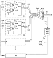
- the block diagram which simplifies and shows the light source device of this invention is represented.
- the block diagram which simplifies and shows the light source device of this invention is represented.
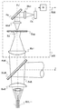
- the schematic diagram which simplifies and shows a part of light source device of this invention is represented.
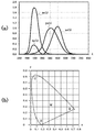
- the schematic of the concept relevant to the technique of the light source device of this invention is represented.
- the schematic of the concept relevant to the technique of the light source device of this invention is represented.
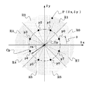
- the schematic of the concept relevant to the technique of the light source device of this invention is represented.
- the block diagram which simplifies and shows a part of light source device of this invention is represented.
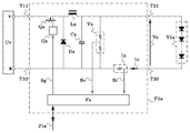
- the schematic diagram which simplifies and shows one form of the one part of the Example of the light source device of this invention is represented.
- the schematic diagram which simplifies and shows one form of the one part of the Example of the light source device of this invention is represented.
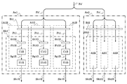
- the figure explaining one form of one part of the kind of the conventional projector concerning the projector of this invention is represented.
- the figure explaining one form of one part of the kind of the conventional projector concerning the projector of this invention is represented.
- FIG. 1 is a block diagram which simplifies and shows the light source device of this invention.
- At least one light emitting element (Y1a, Y1b,%) Provided in the element light source (U1) is driven by a drive circuit (P1a, P1b,%) To emit light.
- a drive circuit P1a, P1b, etc.
- a semiconductor laser or a radiated light of the semiconductor laser is utilized by utilizing a nonlinear optical phenomenon such as harmonic generation or an optical parametric effect.
- a light source for wavelength conversion, etc. which can be driven by one drive circuit (P1a, P1b,...) By connecting a plurality of such light sources in series, in parallel, or in series-parallel connection. It is said.
- the driving circuits (P1a, P1b,...) are DC / DC converters configured by a circuit of a system such as a step-down chopper or a step-up chopper, which is powered by a DC power supply (not shown) here.
- the integrated control circuit (Mc) individually outputs data for each of the drive circuits (P1a, P1b,..., P2a, P2b,...) Via drive circuit control signals (J1a, J1b,..., J2a, J2b,). It is configured to be able to send and receive and control and to supply a prescribed power to each of the light emitting elements (Y1a, Y1b,..., Y2a, Y2b,).
- the light source device of the present invention has a plurality of element light sources similar to the element light source (U1), and the light emitting elements (Y1a, Y1b,..., Y2a, Y2b, etc. Included therein emit light. Wavelengths belonging to a plurality of different narrow wavelength bands are included, and the included wavelength bands are the three primary colors R, G, and B here. Therefore, in order to measure the overall light characteristics of the respective output light beams (Fo1, Fo2,%) Of these element light sources (U1, U2,...), The output light beams (Fo1, Fo2,.
- An output light beam for measurement consisting of an amount of light that correlates with the light amount of the output light beam (Fo1, Fo2,%) Collected by extracting each part is generated and provided for each of the aforementioned wavelength bands. Further, the light is incident on the band light characteristic acquisition means (AiR, AiG, AiB).
- the total light characteristic means that the output light beams (Fo1, Fo2,%) Are separately output when the light in the R, G, B wavelength bands is mixed and output.
- image information is put on light by two-dimensional light amplitude modulation for each wavelength band, and finally, Assuming a state where all of the output light beams (Fo1, Fo2,%) Are mixed, the light content by wavelength band and the respective wavelength bands in the entire output light beam (Fo1, Fo2,%) The characteristics of the entire output light flux (Fo1, Fo2,%) Such as the color of the light.
- Correlation with the light amount of the output light beam means that if the measurement output light beam (Fo ') is measured, the light amount and the hue for each wavelength band of the output light beam (Fo1, Fo2,%) Can be estimated. In this case, even if the correlation magnification (correlation coefficient) is different for each wavelength band, it can be measured and corrected in advance.
- the band light characteristic acquisition means (AiR, AiG, AiB) is for acquiring a light emission intensity instruction value correlated with the light intensity and a wavelength deviation instruction value correlated with a deviation from the reference wavelength.
- the light source device of the present invention can be used in any configuration.
- a part of each of the light fluxes extracted from the output light fluxes (Fo1, Fo2,%) In each wavelength band is collectively used as a measurement output light flux (Fo ′), and the band light characteristic acquisition means is collectively included.
- the single band light characteristic income means set (Ax) is simply described for convenience, and the measurement light flux for each wavelength band is supplied to the band light characteristic acquisition means for each wavelength band.
- the integrated control circuit (Mc) obtains band light characteristic acquisition data (ShR, ShG, ShB) including information for acquiring a light emission intensity instruction value and a wavelength deviation instruction value from the band light characteristic acquisition means (AiR, Read from AiG, AiB).
- the output luminous flux (Fo1, Fo2,%) Illuminates a two-dimensional light amplitude modulation element provided separately for each color of R, G, and B, and a dichroic mirror
- FIG. 2 is a block diagram showing the light source device of the present invention in a simplified manner
- the light emitted from the light emitting elements (Y1a, Y1b,..., Y2a, Y2b,...) Is collected from, for example, a lens.
- the light is focused on the incident end (Ei1, Ei2,%) Of the optical fiber (Ef1, Ef2,%) By the optical optical system (Ec1, Ec2,%) And propagates through the core of the optical fiber (Ef1, Ef2,. It is also possible to radiate from the emission ends (Eo1, Eo2,).
- the radiated light from the emission ends (Eo1, Eo2,%) Of the optical fibers (Ef1, Ef2,%) Of the element light sources (U1, U2,%) are combined into one output light beam (Fo).
- Output from the light source device As a comprehensive method of radiated light from the plurality of emission ends (Eo1, Eo2,%), The simplest method is to place the emission ends (Eo1, Eo2,%) On the same plane. This can be realized by bundling the emission ends of the optical fibers (Ef1, Ef2,). A part of the emitted light from the emission end (Eo1, Eo2,%) So that the amount correlated with the amount of the output light beam (Fo) guided by each of the optical fibers (Ef1, Ef2,%) Can be measured.
- the output light flux for measurement (Fo ') is extracted and integrated, and the band light characteristic income means set (Ax) in which the band light characteristic acquisition means (AiR, AiG, AiB) are grouped together. ).
- the band light characteristic income means set (Ax) in which the band light characteristic acquisition means (AiR, AiG, AiB) are grouped together.
- all the output ends of the optical fibers (Ef1, Ef2,...) Are bundled to generate an output light beam (Fo) of white light.
- the output ends (Eo1, Eo2,...) Are divided and bundled to generate output light fluxes for each wavelength band, which are individually input to the band light characteristic acquisition means (AiR, AiG, AiB). You can also.
- FIG. 3 which is a schematic diagram showing a part of the light source device of the present invention in a simplified manner, shows an example of configuring the band light characteristic acquisition means (AiR, AiG, AiB).
- This figure generates band light characteristic acquisition data (ShR) for acquiring a light emission intensity instruction value correlating with the light intensity in the R color wavelength band and a wavelength deviation instruction value correlating with a deviation from the reference wavelength.
- band light characteristic acquisition means depicted as band light characteristic acquisition means (AiR), the same may be applied to wavelength bands of other colors.
- Radiated light from the output end of the optical fiber (Ef1,...) Is converted into an R-color output light beam (FoR) through an collimator lens (EsR), reflected by a mirror (HuR), and z Guided in the direction of the axis.
- the transmitted light (FoR ′) leaks from the mirror (HuR), which is slightly present in the direction of the z′-axis, the light is leaked from the pinhole (Eap) of the aperture plate (Eap) by the condenser lens (Eb1). Ea) and collect the passing light backward.
- the extracted light beam is converted by the collimator lens (Eb2) from the image of the pinhole (Ea) into a light beam forming an infinite image, and this light beam is used as the output light beam for measurement, and the wavelength of the light contained therein.
- the imaging lens (Eb3) After reflecting with a wavelength dispersive optical element (Eg) using a diffraction grating or the like having a function of changing the traveling direction in accordance with the imaging lens (Eb3), the imaging lens (Eb3) passes through the imaging lens (Eb3). An image of the pinhole (Ea) subjected to spectral decomposition is generated on the output image plane.
- an image pickup surface of an image pickup device (Ca) using, for example, a one-dimensional image sensor or the like is arranged at the position of this image so that this image can be picked up.
- the arrangement direction of the pixels of the imaging element (Ca) coincides with the direction in which the angle of the emitted light changes depending on the wavelength change of the incident light to the wavelength dispersive optical element (Eg) and is projected.
- the signal processing circuit (H) reads the brightness distribution pattern in the above-described spectrally resolved pinhole image acquired by the imaging device (Ca), and the brightness of each pixel.
- To calculate the distribution pattern intensity further calculate the position of the center of gravity of the pattern to determine the amount of deviation from the pixel position corresponding to the reference wavelength, and the band light characteristic comprising the distribution pattern intensity and the amount of deviation Acquisition data (ShR) can be generated.
- the brightness of each pixel is calculated before the calculation of the sum of the brightness of each pixel and the calculation of the centroid position of the distribution pattern. Is preferably corrected depending on the position of each pixel.
- the wavelength resolution is 0.1 mn / pixel and the slope of spectral sensitivity in this wavelength band (ie, the amount of increase in sensitivity when the wavelength is increased by 1 nm) is 2% / nm, it corresponds to the reference wavelength.
- the following formula Kn 1 ⁇ 0.002 ⁇ n
- a value obtained by multiplying the correction coefficient Kn may be corrected so as to be evaluated as true brightness.
- n may be interpreted as negative and corrected by the same equation.
- the signal processing circuit (H) can determine the distribution pattern intensity and the amount of deviation as described above, by combining the radiated light from all the optical fibers (Ef1,%) Related to the wavelength band.
- the position of the pinhole (Ea) in the z′-axis direction needs to be set to a position where the radiated light from all of the optical fibers (Ef1,...) Is superimposed.
- the central axis of the angular distribution of emitted light from each point of the core at the exit end of each of the optical fibers (Ef1,...) That is, the principal ray is the central axis of the core of the optical fiber (Ef1,. Since the entrance pupil of the condenser lens (Eb1) is at infinity, the pinhole (Ea) is placed at the center of the exit pupil of the condenser lens (Eb1). It is preferable to provide it.
- the integrated control circuit (Mc) receives the band optical characteristic acquisition data (ShR, ShG, ShB) from the band optical characteristic acquisition means (AiR, AiG, AiB), thereby allowing each wavelength band of R, G, B
- the distribution pattern intensity and the amount of deviation described above can be acquired for each of the above. Therefore, the integrated control circuit (Mc) calculates emission intensity instruction values Sr, Sg, Sb correlated with the light intensity from the distribution pattern intensity described above for each of the R, G, B wavelength bands.
- the wavelength deviation instruction values ⁇ r, ⁇ g, ⁇ b that correlate with the deviation from the reference wavelength can be calculated from the deviation amount of the center of gravity position of the distribution pattern from the pixel position corresponding to the reference wavelength.
- the color of light emitted from a light source or the like is represented by chromaticity coordinates based on the XYZ color system that is established by CIE.
- CIE Color Engineering Laboratory
- the tristimulus values X, Y, and Z of the light beam to be measured represented by the spectrum S ( ⁇ ) with the wavelength ⁇ as a parameter are the color matching functions xe ( ⁇ ), ye ( ⁇ ), ze () defined by the CIE.
- FIG. 4A is a schematic diagram of the concept related to the technology of the light source device of the present invention.
- the color matching function uses a symbol with a horizontal bar on each of the x, y, and z characters. However, in this specification, it is described as described above for convenience.
- the integrated control circuit (Mc) determines the function value and wavelength at the reference wavelength for each of the color matching functions xe ( ⁇ ), ye ( ⁇ ), and ze ( ⁇ ) for each of the R, G, and B wavelength bands. It holds local band color matching function information consisting of information related to changes in the function value of the color matching function when the wavelength changes from the reference wavelength (for example, the rate of change of the function with respect to the wavelength change described later). Therefore, the integrated control circuit (Mc), as will be described later, is based on the emission intensity instruction value and the wavelength deviation instruction value calculated for each of the R, G, and B wavelength bands. Using the function information, the tristimulus values X, Y, Z or the chromaticity coordinates x, y as the hue instruction values can be approximately calculated.
- FIG. 4B is a schematic diagram showing what is called a chromaticity diagram showing the relationship between chromaticity coordinates and colors. All colors that can be expressed in this color system are shown on the dotted line in the figure. Alternatively, the approximate positions of red (R), green (G), blue (B), and white (W) are described. Note that monochromatic light such as laser light is located on the dotted line in the figure. (However, the straight line from R to B, the so-called pure purple locus is excluded.) The pure white chromaticity coordinates are 1/3 and 1/3.
- the target chromaticity coordinates are not necessarily those corresponding to pure white. This is because, for example, when the light source device is applied to a projector, the light use efficiency of the optical system of the projector main body is not always the same for each of the R, G, and B colors. For example, if the use efficiency of B color is low in an optical system of a projector main body, the target chromaticity coordinates will be blue with a large B color component. Therefore, the target chromaticity coordinates may be determined according to the output of the apparatus using the light source device, not the color of the output light beam (Fo, Fo1, Fo2,...) Of the light source device.
- the integrated control circuit (Mc) correlates with the emission intensity instruction values Sr, Sg, Sb and the deviation from the reference wavelength, which correlate with the light intensity, so that the target hue which is the subject of the present invention can be maintained.
- Wavelength deviation instruction values ⁇ r, ⁇ g, ⁇ b to be obtained are calculated, chromaticity coordinates x, y as hue instruction values are calculated, and compared with their respective target values, and the drive circuits (P1a, P1b,..., P2a) are calculated. , P2b,...), Which drive light emitting elements in the R, G, and B wavelength bands, the total output power Pr, Pg, Pb must be increased or decreased as appropriate to adjust the white balance in a feedback manner.
- a method of calculating the increase / decrease amount of the output power for efficiently performing this adjustment sequence will be described later.
- the XYZ color system which is the establishment of the above CIE is configured such that the Y value of the above-described formula 1 represents the brightness of light that combines all of the included wavelength bands. Therefore, in addition to the hue instruction value that correlates with the color of light, in the case of stabilizing and controlling the brightness of light that combines all the R, G, and B wavelength bands, the integrated control circuit (Mc) The calculated Y value is used as a brightness instruction value, and this is compared with the target value.
- the driving circuit (P1a , P1b,..., P2a, P2b,...)) That drive the light emitting elements in the R wavelength band, and the total output power Pg of those that drive the light emitting elements in the G wavelength band.
- the drive circuit control signals J1a, J1b,..., J2a, J2b,...) So as to decrease (or increase) the total output power Pb of the light-emitting elements in the B wavelength band at the same rate.
- difference feedback control in a direction decreases the brightness of the light and the target value is performed, it is possible to adjust the brightness of the light. A method of calculating the increase / decrease amount of the output power for efficiently performing this adjustment sequence will be described later.
- the total output Pr of the light emitting elements in the R wavelength band, and the G wavelength band is driven, and the total output power Pb of the light-emitting element of the B wavelength band is driven with respect to the light intensity of the components in the R, G, and B wavelength bands.
- the light-emitting efficiency of the light-emitting elements (Y1a, Y1b,..., Y2a, Y2b,...) Is different between the light-emitting elements having different emission colors.
- the same light emitting elements of the light emitting colors are assumed to be all the same luminous efficiency (more practically speaking the same manufacturer of the same type product). Therefore, if the above-mentioned premise is not satisfied due to a mixture of a plurality of types having different luminous efficiencies even in the same color, for example, a light emitting element of type A having a certain light emitting color and having high light emitting efficiency. And a light emitting element of type B whose luminous efficiency is 10% lower than that, the integrated control circuit (Mc) via the drive circuit control signals (J1a, J1b,..., J2a, J2b,).
- the driving circuit that drives the type B light emitting element internally sets the power to be 10% higher than the commanded set power. Therefore, it can be solved easily.
- the power setting for the drive circuit is limited in its fineness, for example, 256 gradations if the setting data length is 8 bits. Therefore, when the power is increased by the minimum unit, the power setting of all the drive circuits is not increased by 1 LSB at the same time, but for example, the power setting of the first drive circuit is increased by 1 LSB, and then the second drive.
- the power setting of the circuit is increased by 1 LSB, the number of drive circuits is increased separately, and the power setting of the last drive circuit is increased by 1 LSB, then the power setting of the first drive circuit is increased by 1 LSB again. ..,..., There is an advantage that the number of gradations for power setting can be increased by a factor of the number of drive circuits.
- the integrated control circuit (Mc) correlates with the light intensity based on the band light characteristic acquisition data (ShR, ShG, ShB) from the band light characteristic acquisition means (AiR, AiG, AiB).
- the emission intensity instruction value to be measured is measured.
- the light intensity correlates with the optical power of all the light emitting elements (Y1a, Y1b,..., Y2a, Y2b,...) Belonging to one wavelength band, Is irrelevant.
- the brightness of light is the brightness perceived by humans, even if the light power (density) is the same, the size changes under the influence of human visual sensitivity if the wavelength changes.
- the emission intensity instruction values of the R, G, B wavelength bands are in the drive circuit (P1a, P1b,..., P2a, P2b,...)
- the total output power Pr for driving the light emitting elements in the R wavelength band, the total output power Pg for driving the light emitting elements in the G wavelength band, and the total output power for driving the light emitting elements in the B wavelength band It may be considered that each Pb is proportional to each other independently. For example, when the emission intensity instruction values of the R, G, and B wavelength bands are all increased by 1%, if the total output power is 200 W, 300 W, and 100 W, respectively, 202 W, 303 W, 101W may be used.
- the total output Pr of the light emitting elements in the R wavelength band and the G wavelength are the emission intensity instruction values for the R, G, and B wavelength bands, respectively.
- the emission intensity instruction values Sr, Sg, Sb calculated based on the band light characteristic acquisition data (ShR, ShG, ShB) acquired by the band light characteristic acquisition means (AiR, AiG, AiB) From the ratios of Pr, Pg, and Pb, the proportional coefficients kr, kg, and kb of Equation 3 can be determined. First, assuming that the proportional coefficients kr, kg, kb are set as uncertain but appropriately determined safe initial values, the emission intensity instruction values Sr, kr, kb are determined based on the undetermined kr, kg, kb.
- Pr, Pg, and Pb that will give rise to suitably defined safe initial target values Srp, Sgp, and Sbp for Sg and Sb are provisionally determined by the above-described equation (3).
- proportional coefficients kr, kg, and kb are expressed by the following equations (Formula 4).
- the chromaticity coordinates x, y are obtained by using the emission intensity instruction values Sr, Sg, Sb specifically obtained and the deviations ⁇ r, ⁇ g, ⁇ b from the reference wavelength as the wavelength deviation instruction values. And a method of calculating the light brightness Y, and further, the emission intensity instruction value Sr for performing feedback control so that the chromaticity coordinates x, y and the light brightness Y are maintained at the target values.
- Sg, Sb When changing minutely, the method of determining the change amounts ⁇ Sr, ⁇ Sg, ⁇ Sb will be described.
- the integrated control circuit (Mc) As information on the change in the function value of the color matching function when the wavelength is changed from the reference wavelength, for example, each of the wavelength bands described above With respect to, the color matching function value at a discrete wavelength value appropriately selected in the vicinity of the reference wavelength is held, and the function value corresponding to the measured wavelength deviation indication value is obtained with the aid of an interpolation method. can do.
- the change in wavelength of the light-emitting elements (Y1a, Y1b,..., Y2a, Y2b,...) Due to the temperature change or the like is, for example, on the order of several nanometers. Even if the function form is approximated to be a straight line, the practical accuracy can be sufficiently obtained.
- the change amount of the hue indication value when the emission intensity indication value for each of the wavelength bands described above is slightly changed is expressed by the linear calculation using the change amount of the emission intensity indication value.
- the coefficient at that time could be determined using the emission intensity instruction value and the wavelength deviation instruction value for each of the wavelength bands described above.
- the calculation method using the values ⁇ r, ⁇ g, ⁇ b from the obtained reference wavelength was presented.
- the values of these coefficients can be determined by approximating the deviations ⁇ r, ⁇ g, and ⁇ b from the reference wavelength all zero.
- the values corresponding to Ir, Ig, Ib and Equation 21 in the above-described equation 18 regarding the chromaticity coordinates x, y are the deviation ⁇ r from the reference wavelength.
- Equation 28 the following equation (Equation 28) is used as an equation to be solved in the feedback control loop.
- ⁇ x, ⁇ y, ⁇ Y on the left side are based on the chromaticity coordinates, the target values xp, yp, Yp of the lightness instruction value Y, and the values of x, y, Y at that time, and the above equation 23 It may be calculated by
- the light emission intensity instruction values Sr, Sg, Sb can be excluded from the equation 28, and feedback control can be performed in which only the chromaticity coordinates x and y are maintained at the target values.
- a plurality of modes relating to the appearance modes are assumed in advance, and each appearance mode is assumed.
- the emission intensity instruction values Sr, Sg, Sb obtained by measurement and the deviations ⁇ r, ⁇ g, ⁇ b from the reference wavelength as the wavelength deviation instruction values are obtained.
- the chromaticity coordinates x and y as the current hue instruction value and the brightness Y of the light are calculated, and the difference between the hue instruction value and its target value, that is, the current chromaticity coordinate difference vectors ⁇ x and ⁇ y are calculated.
- a similar one is selected from a plurality of chromaticity coordinate difference vectors (representative points to be described later) assumed in advance.
- a plurality of patterns of chromaticity coordinate difference vectors ⁇ x and ⁇ y as a plurality of modes related to appearances of the above-described differences.
- the entire range 0 to 2 ⁇ (unit: radians: ⁇ is the circumference) in which the deviation angles of the chromaticity coordinate difference vectors ⁇ x and ⁇ y can appear is divided into a plurality of small ranges, A representative point having a normalized absolute value (radius) is set for each small range, and the solution of the equation for each representative point, that is, the amount of change ⁇ Sr, ⁇ Sg, ⁇ Sb of the corresponding emission intensity indication value is set. The combination is calculated and stored.
- Sbp Sb + ⁇ Sb
- ⁇ Y Hyro ⁇ ⁇ Sr + Hybo ⁇ ⁇ Sb Therefore, the value Y is maintained at the target value Yp by multiplying Sr, Sg and Sb by a common ratio ⁇ so as to cancel out this change. Can be.
- ⁇ ′ 1 ⁇ D ′ ⁇ ⁇ Y + ⁇ Y ⁇ / Yp It can be approximated as follows. Even if ⁇ Y is not very small, this calculation is repeatedly performed in the feedback control loop, so that Y is asymptotic to Yp and eventually becomes fine, so there is no problem.
- ⁇ Srn ⁇ Nybo ⁇ ⁇ x + Nxbo ⁇ ⁇ y ⁇ / no
- ⁇ Sbn ⁇ Nyro • ⁇ x ⁇ Nxro • ⁇ y ⁇ / no
- FIG. 5 is a schematic diagram of a concept related to the technology of the light source device of the present invention.
- This figure is a ⁇ x, ⁇ y coordinate system in which the coordinates xp, yp of the chromaticity target values taken on the chromaticity diagram are local origins (Op), and the x, y coordinate system is related by the above-described equation 41. It is attached.
- the region to which the coordinate point (P) corresponding to the current difference ⁇ x, ⁇ y from the target value of chromaticity coordinates belongs is divided into, for example, eight types, and here, 0, ⁇ around the local origin (Op) in the counterclockwise direction / 4, ⁇ / 2, 3 ⁇ / 4, ⁇ , 5 ⁇ / 4, 3 ⁇ / 2, and 7 ⁇ / 4 are divided into declination regions (R0, R1,..., R7). Further, as shown in the figure, the angle centers of the respective deflection angle regions, that is, deflection angles of ⁇ / 8, 3 ⁇ / 8, 5 ⁇ / 8, 7 ⁇ / 8, 9 ⁇ / 8, 11 ⁇ / 8, 13 ⁇ / 8, and 15 ⁇ / 8.
- a representative point (p0, p1,..., p7) on a normalized circle (Cp) having ⁇ and centering on the local origin (Op) and having a normalized radius rn is set. Then, the values ⁇ Srn and ⁇ Sbn of the equation 43 are calculated in advance for all ⁇ x and ⁇ y of the representative points (p0, p1,..., P7), and the microprocessor of the integrated control circuit (Mc) is calculated.
- the above-mentioned normalized radius rn may be an appropriate size. For example, the short axis length (about 0.001) or the long axis length (about 0) of the so-called MacAdam color matching ellipse near pure white. .002), for example, 0.005. (Reference: David L. MacAdam, JOSA Vol.32 May.1942 Fig.35)
- the calculation procedure is as follows. First, after determining the target values xp, yp of the chromaticity coordinates and applying them to the x, y of the above-described equation 30, the coefficients Nxro, Nxgo, Nxbo, Nyro, Nygo in the vicinity of the target chromaticity coordinates are determined. , Nybo is determined in advance.
- the above-described pre-calculation is performed by, for example, a personal computer, and the above-described array of normalized solutions ⁇ Srn and ⁇ Sbn, which is calculation result data, is transferred to the integrated control circuit (Mc) of the light source device of the present invention. You can do it.
- Mc integrated control circuit
- the chromaticity coordinate difference vectors ⁇ x, ⁇ y are determined according to Equation 41 described above.
- This chromaticity coordinate difference vector corresponds to which of the representative points (p0, p1,..., P7) when focusing on the declination in the ⁇ x, ⁇ y coordinate plane of FIG. It is necessary to determine whether they are similar, but this can be determined by the following operation.
- j For an integer auxiliary variable j for index calculation: j ⁇ 0 If ⁇ y> 0, j ⁇ j + 4 If ⁇ x> 0, j ⁇ j + 2 If abs ( ⁇ y)> abs ( ⁇ x) then j ⁇ j + 1 (Note that abs () is a function that returns an absolute value)
- the value of j as a result of performing four operations is a value between 0 and 7, for example, corresponding to 0 of the index i described above.
- ⁇ Sr D ⁇ ⁇ Srn [C [j]] ⁇ T ⁇ ⁇ r / rn
- ⁇ Sb D ⁇ ⁇ Sbn [C [j]] ⁇ T ⁇ ⁇ r / rn
- Equation 50 By applying the solution of Equation 50 thus obtained to Equation 38 described above, the values of the target values Srp, Sgp, and Sbp of Sr, Sg, and Sb can be updated. Further, when one of the light emission intensity instruction values Sr, Sg, Sb is determined separately for some reason, the solution of the equation 50 obtained as described above is once given to the equation 34. Assuming that the values of Srp, Sgp, and Sbp obtained by application are now written as Srp ′, Sgp ′, and Sbp ′, for example, when setting the value of Sb to the specified value Sbf, the value of the ratio Sbf / Sb ′ is set.
- the values obtained by calculating and multiplying the provisional values Srp ′, Sgp ′, and Sbp ′ by the calculation may be updated as new Srp, Sgp, and Sbp, respectively.
- Sr and Sg can be calculated in the same manner.
- the integrated control circuit (Mc) is calculated based on the band light characteristic acquisition data (ShR, ShG, ShB) acquired by the band light characteristic acquisition means (AiR, AiG, AiB).
- the proportional coefficients kr, kg, kb are updated by applying the emission intensity instruction values Sr, Sg, Sb and the original target values Srp, Sgp, Sbp to the equation (4).
- the integrated control circuit (Mc) applies the solution of the equation 50 to the equation 38 or 34 to the current values Sr, Sg, Sb of the emission intensity instruction value, and sets the emission intensity instruction value.
- New target values Srp, Sgp, Sbp are calculated, and the electric powers Pr, Pg, Pb of the drive circuits (P1a, P1b,..., P2a, P2b,...) Are updated according to Equation 3. Then, the operation returns to the operation of acquiring the band light characteristic acquisition data (ShR, ShG, ShB), and thereafter, the feedback control loop is constructed by repeating the described sequence.
- the values of the tristimulus values X, Y, and Z on the left-hand side of the equation 25 are the band light characteristic acquisition data acquired by the band light characteristic acquisition means (AiR, AiG, AiB) as described above.
- the emission intensity instruction values Sr, Sg, Sb and deviations ⁇ r, ⁇ g, ⁇ b from the reference wavelength as the wavelength deviation instruction values are obtained.
- the emission intensity instruction values Sr, Sg, and Sb to be applied to the above Equations 4 and 5 are obtained by solving the above Equation 25 as an equation. You can also use different values.
- the combination information of the change amount of the emission intensity instruction value obtained by the above-described previous calculation corresponding to the selected chromaticity coordinate difference vector is extracted, and the change value of the corresponding emission intensity instruction value is obtained.
- the following is a summary of the feedback control method for obtaining.
- the integrated control circuit (Mc) determines appropriate initial target values Srp, Sgp, and Sbp for the emission intensity instruction values Sr, Sg, and Sb in the R, G, and B wavelength bands, respectively, and is proportional.
- Appropriate initial values of the coefficients kr, kg, kb are determined, and the electric power Pr, Pg, Pb of the drive circuit (P1a, P1b,..., P2a, P2b,...) Is set according to the expression 3 to set the light emitting elements (Y1a, Y1b). ,..., Y2a, Y2b,.
- the emission intensity instruction values Sr, Sg, Sb calculated based on the band light characteristic acquisition data (ShR, ShG, ShB) acquired by the band light characteristic acquisition means (AiR, AiG, AiB), and the original target value Srp, Sgp, and Sbp are applied to Equation 4 to update the proportional coefficients kr, kg, and kb.
- the emission intensity instruction values Sr, Sg, and Sb and the deviations ⁇ r, ⁇ g, and ⁇ b from the reference wavelength, which are the wavelength deviation instruction values, are applied to Equations 12, 13, 14, and 18, respectively.
- the tristimulus values X, Y, Z and T are determined via the coefficients Hxro, Hxgo, Hxbo, Hyro, Hygo, Hybo, Hzro, Hzgo, Hzbo and applied to equation 19 above to determine the chromaticity.
- the values of the coordinates x, y can be determined, i.e. measured.
- Equation 48 For the chromaticity coordinate difference vectors ⁇ x and ⁇ y of Equation 41, when the index calculation auxiliary variable j is obtained based on Equation 46, the index conversion constant array C of Equation 47 is used as shown in Equation 48. , ⁇ Srn [0], ⁇ Srn [1],..., ⁇ Srn [7] and ⁇ Sbn [0], ⁇ Sbn [1],. Thus, a normalized solution of ⁇ Sr, ⁇ Sb that matches the measured chromaticity coordinates x, y is obtained.
- the integrated control circuit (Mc) applies the solution of the above equation 50 to the equation 38 or 34 described above for the current values Sr, Sg, Sb of the emission intensity instruction values, thereby obtaining a new emission intensity instruction value.
- Target values Srp, Sgp, Sbp are calculated, and the electric powers Pr, Pg, Pb of the drive circuits (P1a, P1b,..., P2a, P2b,...) Are updated according to Equation 3. Then, the operation returns to the operation of acquiring the band light characteristic acquisition data (ShR, ShG, ShB), and thereafter, the feedback control loop is constructed by repeating the described sequence.
- a plurality of modes relating to the appearance modes are assumed in advance.
- the light source device is configured so as to obtain combination values of the change amounts ⁇ Sr, ⁇ Sg, ⁇ Sb of the corresponding emission intensity instruction values by taking out the combination information of the change amounts of the emission intensity instruction values obtained by the calculation. Efficient feedback control can be performed without installing a simple microprocessor.
- the target values xp, yp and Yp of the feedback control will be supplemented.
- various approximate calculations are performed on the assumption that the purpose of calculation of chromaticity coordinates and the like in this light source device is not to determine an accurate absolute value. Therefore, even if the target values xp, yp, Yp are given numerically, it is unclear whether or not the state achieved by feedback control will be a desired one, and such usage is not appropriate.
- this light source device is actually mounted on the actual projector, and an image that should be white is projected on the screen with feedback control stopped so that a desired white color can be obtained.
- the light intensity of each of R, G and B of the light source device is manually adjusted, and when the adjustment is completed, the measured values of x, y and Y by the light source device itself are obtained as target values xp, yp and Yp. It is good to memorize as.
- the actual value of the stored target value may be neglected, and thereafter, a state in which a desired white color is obtained is achieved by executing feedback control.
- the light emission intensity instruction value Sg of G color is given as an example, and in order to explain the handling when this or ⁇ Sg is excluded from the unknown of the expression 22 described above, the above expression 24 is described. Then, the combination information of the change amount of the emission intensity instruction value obtained by the above-described previous calculation corresponding to the selected chromaticity coordinate difference vector is taken out, and the change value of the corresponding emission intensity instruction value is obtained.
- the above-described formula 31 corresponding to the starting point in the description of the calculation method for obtaining the formula is obtained by modifying the above-described formula 24.
- the number of unknown equations to be solved is reduced from three of ⁇ Sr, ⁇ Sg and ⁇ Sb to two of ⁇ Sr and ⁇ Sb. It was to reduce. Therefore, in these calculations, there is no necessity to select the G color as an object to be excluded from the unknown in the equation.
- the R color or the B color may be selected and excluded from the unknown.
- the calculation method can be determined in exactly the same way.
- the number of the representative points (p0, p1,..., P7) prepared in the two-dimensional space of ⁇ x, ⁇ y prepared for the two unknowns described above is eight. If the same division is performed in the case of the number of pieces, since the selection is made in the three-dimensional space of ⁇ x, ⁇ y, and ⁇ Y, the number of representative points is 32.
- the light source device of the present invention may be configured so that the number of unknowns in the equation is three unless there is a large number of solutions to be prepared by calculation in advance for selection. .
- the division of the existence area of the coordinate point (P) an example of dividing into eight areas such as the declination areas (R0, R1,..., R7) is illustrated.
- the number may be increased to, for example, 16 divisions, or may be decreased to, for example, 4 divisions.
- the existence area is divided by focusing only on the declination regardless of the distance ⁇ r of the coordinate point (P) from the local origin (Op).
- the region is divided into polar declination regions (R0, R1,..., R7) centered on the local origin (Op), and the representative points (p0, p1) of each region are divided. ,..., P7) are set, and the normalized solution values ⁇ Srn and ⁇ Sbn of Equation 43 are calculated and stored in advance for all ⁇ x and ⁇ y of the representative points (p0, p1,..., P7).
- a representative point close to the coordinate point (P) is selected from the representative points (p0, p1,..., P7), and By correcting the normalized solution belonging to the representative point selected by the above equation 50 according to the ratio of the distance between the coordinate point (P) and the local origin (Op) to the distance of the local origin (Op), A method of obtaining the solutions ⁇ Sr and ⁇ Sb for the coordinate point (P) of the above has been described.
- the division of the region is not limited to the polar coordinate method as described above. For example, as shown in FIG. 6, the region is divided into quadrature rectangular regions and arranged in a lattice pattern in the same manner as described above.
- the value ⁇ Srn of the normalized solution of Equation 43 described above for all ⁇ x, ⁇ y of the representative points (p0, p1,..., P15). , ⁇ Sbn are calculated and stored in advance, and when obtaining the solutions ⁇ Sr, ⁇ Sb for the actual coordinate point (P), the coordinate point (P) is selected from the representative points (p0, p1,..., P15).
- a close representative point is selected, and belongs to the representative point selected by the equation 50 according to the ratio of the distance between the coordinate point (P) and the local origin (Op) to the distance between the local origin (Op) and the local representative point.
- the actual coordinate point (P) is corrected.
- Solution .DELTA.Sr can be obtained .DELTA.SB.
- the representative point (p14) may be selected.
- the band light characteristic acquisition unit of the light source device As the band light characteristic acquisition unit of the light source device, the band light characteristic acquisition unit (AiR) for measuring the wavelength deviation instruction value using the wavelength dispersive optical element (Eg) illustrated in FIG.
- the band light characteristic acquisition means applicable to the light source device of the present invention is not limited to this.
- the band light characteristic acquisition means (AiR, AiG, AiB) of at least one of the above-described wavelength bands has a first spectral characteristic for spectral sensitivity characteristics in the wavelength band.
- the first light quantity measuring means (A1R, A1G, A1B) having sensitivity characteristics and the second light quantity measuring means (A2R, A2G, A2B) having second spectral sensitivity characteristics are configured as described above.
- the spectral sensitivity characteristic of 1 and the above-described second spectral sensitivity characteristic are different in the rate of change of sensitivity with respect to a change in wavelength, that is, the slope of the sensitivity change at the time of wavelength change.
- 1 spectral sensitivity characteristic and local spectral sensitivity comprising the sensitivity value at the reference wavelength and the rate of change in sensitivity with respect to the change in wavelength described above for each of the second spectral sensitivity characteristics described above.
- First light quantity measurement data (Sh1R, Sh1G, Sh1B) generated by the first light quantity measurement means (A1R, A1G, A1B), which holds information and is the band light characteristic acquisition data (ShR, ShG, ShB)
- second light quantity measurement data (Sh2R, Sh2G, Sh2B) generated by the second light quantity measurement means (A2R, A2G, A2B), which is the band light characteristic acquisition data (ShR, ShG, ShB).
- FIG. 7 is a block diagram showing a part of the light source device of the present invention in a simplified manner.
- the band light characteristic acquisition means (AiR, AiG, AiB) of at least one wavelength band out of the above-described wavelength bands has a first spectral sensitivity characteristic for the wavelength band.
- the first light quantity measuring means having the spectral sensitivity characteristic and the second light quantity measuring means having the second spectral sensitivity characteristic are configured.
- the band light characteristic obtaining means (AiR) for all wavelength bands is used.
- AiG, AiB) are assumed to be configured as just described.
- the measurement output light beam (Fo ') is input to the first light quantity measurement means (A1R, A1G, A1B) provided for each of the wavelength bands described above, and the same
- the measurement output light beam (Fo ') is drawn into the second light quantity measuring means (A2R, A2G, A2B) provided for each of the wavelength bands described above.
- the first light quantity measuring means (A1R, A1G, A1B) in the R, G, B wavelength bands are collectively referred to as a first light quantity measuring means group (Ax1), and each of the R, G, B wavelengths.
- the second light quantity measuring means (A2R, A2G, A2B) in the band are drawn together as a second light quantity measuring means group (Ax2) for convenience of convenience.
- Ax2 the first light quantity of R color
- the measurement means and the second light quantity measurement means are grouped together, the G color first light quantity measurement means and the second light quantity measurement means are grouped together, and the B color first light quantity measurement means and the second light quantity measurement means are further arranged. You may make it collectively.
- the band light is divided from the output light beam (Fo ′) for measurement obtained by collecting a part of each light beam extracted from the output light beam (Fo1, Fo2,...) In each wavelength band.
- the output light flux for measurement for each wavelength band is not grouped, but the band light characteristic acquisition means (AiR) for each wavelength band. , AiG, AiB) may be directly input.
- the measurement output light beam (Fo ′) is input to the characteristic filter (Et1), and the measurement output light beam (Ft1) that has passed therethrough is R. , G, B3 band filters (Et1R, Et1G, Et1B), and light is received by photosensors (C1R, C1G, C1B) for each color.
- the light detection signals (Sg1R, Sg1G, Sg1B) from the optical sensors (C1R, C1G, C1B) are subjected to necessary processing such as amplification and AD conversion by a signal processing circuit (H1R, H1G, H1B), and R, G , B, first light quantity measurement data (Sh1R, Sh1G, Sh1B) including information on the quantity of light in each wavelength band is generated.
- the spectral sensitivity characteristics of the first light quantity measuring means (A1R, A1G, A1B) include the light caused by the characteristic filter (Et1) and the bandpass filters (Et1R, Et1G, Et1B).
- the characteristic filter (Et1) is described as being configured to provide a common one for each of the first light quantity measurement means (A1R, A1G, A1B), the first light quantity measurement means ( A1R, A1G, and A1B) may be individually provided.
- the signal processing circuits (H1R, H1G, H1B) are configured so as to be provided individually for each of the light detection signals (Sg1R, Sg1G, Sg1B), a selection signal is described.
- an analog multiplexer for selecting one of the light detection signals (Sg1R, Sg1G, Sg1B) according to the above, and a common one for each of the light detection signals (Sg1R, Sg1G, Sg1B) May be.
- a characteristic filter (Et2) having a different spectral sensitivity characteristic is provided, and the optical sensor circuit section at the subsequent stage.
- the band filters (Et1R, Et1G, Et1B) and the optical sensors (C1R, C1G, C1B) of the first light quantity measuring means (A1R, A1G, A1B), the signal processing circuits (H1R, H1G) , H1B) and the same optical sensor circuit unit (Ah1) may be used to generate second light quantity measurement data (Sh2R, Sh2G, Sh2B).
- the integrated control circuit (Mc) can read the first light quantity measurement data (Sh1R, Sh1G, Sh1B) and the second light quantity measurement data (Sh2R, Sh2G, Sh2B).
- the characteristic filters (Et1) and the band filters (Et1R, Et1G, Et1B) of the first light quantity measuring means (A1R, A1G, A1B) are not divided and the band filters (Et1R, Et1G, Et1B). Each may also be configured to have the function of the characteristic filter (Et1). This is the same for the band filters of the second light quantity measuring means (A2R, A2G, A2B).
- any one of the characteristic filters of the first light quantity measurement means (A1R, A1G, A1B) or the second light quantity measurement means (A2R, A2G, A2B) may be transparent.
- the optical sensor when the output luminous flux (Fo1, Fo2,%) Is divided into R, G, and B colors and used independently for each color, the optical sensor ( Each of C1R, C1G, and C1B) may be configured as a separate body instead of being mounted together in the single optical sensor circuit portion (Ah1).
- the second spectral sensitivity characteristic of A2B) is only required to realize a state in which the rate of change in sensitivity with respect to a change in wavelength, that is, the slope of the change in sensitivity at the time of wavelength change is different in each wavelength band.
- the spectral sensitivity characteristic means a set of a spectral sensitivity characteristic in the R color wavelength band, a spectral sensitivity characteristic in the G color wavelength band, and a spectral sensitivity characteristic in the B color wavelength band in this case.
- the difference in sensitivity change rate with respect to wavelength change in one wavelength band is that one is positive and the other is negative, or one is substantially zero and the other is non-zero (finite value).
- the aforementioned bandwidth is usually Is only a few nanometers to about 10 nanometers, but for each of the first spectral sensitivity characteristic and the second spectral sensitivity characteristic, the change in the rate of change of sensitivity with respect to the change in wavelength within this bandwidth. It is desirable that there are few.
- the integrated control circuit (Mc) sets the sensitivity value at the reference wavelength for each of the R, G, and B wavelength bands for each of the first spectral sensitivity characteristic and the second spectral sensitivity characteristic. It possesses local band spectral sensitivity information composed of the rate of change of sensitivity with respect to the change in wavelength described above. Therefore, as described below, the integrated control circuit (Mc) reads the first light quantity measuring means (A1R, A1G, A1B) and the second light quantity measuring means (A2R, A2G, A2B).
- the local band spectral sensitivity information is used for each of the R, G, B wavelength bands.
- the emission intensity instruction value correlated with the light intensity and the wavelength deviation instruction value correlated with the deviation from the reference wavelength can be calculated approximately.
- the first light quantity measuring means (A1R, A1G, A1B) and the second light quantity measuring means (A2R, A2G, A2B) are converted into a measured light beam represented by a spectrum S ( ⁇ ) having a wavelength ⁇ as a parameter.
- ⁇ a spectrum S having a wavelength ⁇ as a parameter.
- the first light quantity measuring means (A1R, A1G, A1B) has spectral sensitivity characteristics rm ( ⁇ ), gm ( ⁇ ), bm ( ⁇ ) in the R, G, B wavelength bands, the first light quantity measurement.
- the light quantity measurement data values Rm, Gm, Bm in the R, G, B wavelength bands included in the data (Sh1R, Sh1G, Sh1B) are expressed by the following formulas (formula 51).
- Rm ⁇ S ( ⁇ ) ⁇ rm ( ⁇ ) ⁇ d ⁇
- Gm ⁇ S ( ⁇ ) ⁇ gm ( ⁇ ) ⁇ d ⁇
- Bm ⁇ S ( ⁇ ) ⁇ bm ( ⁇ ) ⁇ d ⁇
- the light quantity measurement data values Rn, Gn, Bn in the R, G, B wavelength bands included in the two light quantity measurement data (Sh2R, Sh2G, Sh2B) are expressed by the following equations (formula 52).
- the above-described expression 11 using the delta function ⁇ ( ⁇ ), that is, Record) S ( ⁇ ) Sr ⁇ ⁇ ( ⁇ ro ⁇ r) + Sg ⁇ ⁇ ( ⁇ - ⁇ go- ⁇ g) + Sb ⁇ ⁇ ( ⁇ - ⁇ bo- ⁇ b)
- the reference wavelengths of R, G, and B are ⁇ ro, ⁇ go, and ⁇ bo
- the deviation from the reference wavelength that is the wavelength deviation instruction value is ⁇ r, ⁇ g, ⁇ b, and each of the R, G, and B wavelength bands.
- the emission intensity instruction values of Sr, Sg, and Sb were used.
- Local band spectral sensitivity information on the first light quantity measuring means that is, spectral sensitivity characteristics rm ( ⁇ ), gm ( ⁇ ) at the reference wavelengths ⁇ ro, ⁇ go, ⁇ bo of the R, G, B wavelength bands.
- rn ( ⁇ ro), gn ( ⁇ gn), bn ( ⁇ bn) and sensitivity change rate values Erno, Egno, Ebno with respect to changes in wavelength of spectral sensitivity characteristics are prepared in advance.
- the light quantity measurement data values Rm, Gm, Bm by the first light quantity measurement means (A1R, A1G, A1B) and the light quantity measurement data values Rn, Gn, Bn by the second light quantity measurement means (A2R, A2G, A2B) are obtained.
- the light emission intensity instruction values Sr, Sg, Sb and the deviations ⁇ r, ⁇ g, from the reference wavelength as the wavelength deviation instruction values can be easily obtained by solving the equations consisting of the above-described expressions 54, 55, 56. ⁇ b can be obtained.
- light-emitting elements such as semiconductor lasers have a simple configuration, that is, low-cost band-light characteristics, utilizing the property that the emission wavelength changes due to environmental temperature changes or temperature increases due to self-heating.
- An acquisition means can be realized.
- This band light characteristic acquisition means detects the temperature of the light emitting element that supplies the light of the wavelength band in addition to the light amount detector that detects the light amount of the measurement output light beam (Fo ') for one wavelength band.
- the band light characteristic acquisition data is generated so as to include light amount data detected by the light amount detector and temperature data detected by the temperature detector, while the integrated control
- the circuit (Mc) is configured to hold correlation data between the temperature of the light emitting element and the change of the emission wavelength, thereby including the integration including the case where the correlation between the change of the temperature and the change of the emission wavelength is not linear.
- the control circuit (Mc) uses the emission intensity indication value correlated with the light intensity and the reference wavelength for the wavelength band. It is possible to obtain a wavelength difference indication value of the estimated that correlates to the deviation. Needless to say, it is not necessary to integrally form the light amount detector and the temperature detector that constitute the band light characteristic acquisition means just described.
- the light emitting element is configured to be held in thermal contact with a heat sink having an electric cooling mechanism such as an air-cooled type, a water-cooled type, or a Peltier element for releasing a self-heating amount due to energization, and the light emitting element
- a groove is provided in a part on the light emitting element side or the heat sink side of the surface where the element and the heat sink contact, and the temperature detector is housed in the groove.
- a thermistor, a thermocouple, a semiconductor temperature sensor, or the like can be used as the temperature detector.
- the light emission at a predetermined reference temperature is performed for the reason described for the variation in the light emission wavelength.
- the temperature change from the average value of the total wavelength of all the light emitting elements belonging to the same wavelength band at the reference temperature depending on the emission wavelength of each element and the amount of change in temperature from the reference temperature for the light emitting element.
- the change in the average value of the wavelengths can be calculated, and therefore the total wavelength deviation indication value can be estimated.
- the wavelength deviation instruction value estimated based on the detected temperature of each temperature detector is in charge. It is desirable to calculate the total wavelength deviation instruction value by a weighted average calculation weighted by an amount correlated with the light emitting element power, for example, a current value. In the simplest case, it is possible to estimate the total wavelength deviation instruction value by calculating the average value of the detected temperatures of each of the temperature detectors (the weighted average weighted by the amount correlated with the light emitting element power).
- the spectral sensitivity characteristic of the light quantity detector is not flat in the wavelength band, it is desirable to correct the light quantity data detected by the light quantity detector based on the total wavelength deviation instruction value just calculated. .
- the slope of the spectral sensitivity in the wavelength band is 2% / nm and the calculated total wavelength deviation instruction value is 3 nm, the slope of the spectral sensitivity described above is included in this total wavelength deviation instruction value.
- the light quantity data may be corrected by multiplying 0.94 calculated by subtracting the value obtained by multiplying by 1 from the light quantity data detected by the light quantity detector.
- the main factor of the temperature change of the light emitting element is a temperature increase due to self-heating due to the input power from the drive circuit, and conversely, the temperature increase correlates with the power input to the light emitting element.
- This band light characteristic acquisition means detects the power of the light emitting element that supplies light in the wavelength band in addition to the light amount detector that detects the light amount of the measurement output light beam (Fo ') for one wavelength band.
- the band light characteristic acquisition data is generated so as to include the light amount data detected by the light amount detector and the power data detected by the power detector, while the integrated control The circuit (Mc) is configured so as to hold correlation data between the power of the light emitting element and the change in the emission wavelength, so that the integration including the case where the correlation between the change in the power and the change in the emission wavelength is not linear.
- the control circuit (Mc) uses the emission intensity indication value correlated with the light intensity and the reference wavelength for the wavelength band. It is possible to obtain a wavelength difference indication value of the estimated that correlates to the deviation.
- each of the drive circuits (P1a, P1b,..., P2a, P2b,%) Can apply a prescribed power to the light emitting elements (Y1a, Y1b,..., Y2a, Y2b, etc. Therefore, if it has power detection means for detecting the input power to the light emitting element that it drives, it obtains the wavelength deviation instruction value as described above. It can also serve as a power detector. Therefore, at this time, the drive circuits (P1a, P1b,..., P2a, P2b,...) Also serve as a part of the function of the band light characteristic acquisition means (AiR, AiG, AiB).
- (Mc) is a part of the band light characteristic acquisition data (ShR, ShG, ShB) via the drive circuit control signals (J1a, J1b,..., J2a, J2b,...) And the drive circuits (P1a, P1b). ,..., P2a, P2b,.
- the current value that flows through the light emitting element and the voltage value that is generated when the current flows are also correlated with the electric power that is input to the light emitting element, these current value and voltage value are represented by the wavelength deviation indication value. Can be substituted as the value of the detected power to obtain
- the detected power of the light emitting element is an alternative to the temperature of the light emitting element, the matters described in the case of estimating the total wavelength deviation indication value based on the temperature of the light emitting element described above are targeted. It is established directly from temperature to electric power.
- the same wavelength in the reference power can be obtained by the emission wavelength of each of the light emitting elements at a predetermined reference power and the amount of change in the power from the reference power for the light emitting element. It can be said that the change in the average wavelength value accompanying the power change can be calculated from the average wavelength value of all the light emitting elements belonging to the band, and therefore the total wavelength deviation instruction value can be estimated.
- the processing when the spectral sensitivity characteristic of the light quantity detector is not flat in the wavelength band may be performed in the same manner.
- the light emitting element since the light emission wavelength of the light emitting element changes depending on the environmental temperature in addition to the self-heating amount, the light emitting element further includes a temperature detector for detecting the environmental temperature, and the detected temperature is used to estimate the wavelength deviation instruction value based on the power. Correction can be added. If the correlation between the power values of the plurality of light emitting elements and the wavelength deviation instruction value is linear, the total wavelength deviation instruction value may be estimated from the average value of the detected power values.
- the temperature detector or power In addition to the detector, it is necessary to provide a light amount detector as described above.
- the light amount detector not only a device that detects the amount of light but also an image sensor can be used.
- the measurement output light beam (Fo ′) is white light in which R, G, and B are mixed.
- the measurement output light beam (Fo ′) is white light in which R, G, and B are mixed.
- optical fiber is made of fragile glass such as quartz, there is a drawback that there is a risk of breakage.
- the optical fiber breaks, the optical power leaks from the breakage point and is absorbed by the coating material provided to mechanically protect the optical fiber, and the coating material may burn out. If it happens, it will be necessary to take a safety measure to detect it and turn off the light emitting element.
- dividing the light of the same color into a plurality of optical fibers is advantageous from the standpoint of safety and configuration of the optical system.
- FIG. 8 and FIG. 9 which are schematic diagrams showing a simplified form of a part of an embodiment of the light source device of the present invention, and as a mode for carrying out the present invention, the light source device of the present invention.
- a specific configuration of the driving circuit and a specific configuration of the projector of the present invention using the light source device of the present invention, particularly after the optical fiber and its emission end will be described.
- the drive circuit (P1a) shown in FIG. 8 is exemplified by one of the drive circuits (P1a, P1b,..., P2a, P2b,...) Of the light source device of the present invention.
- the drive circuit (P1a) based on a step-down chopper circuit operates by receiving a voltage from a DC power supply (Uv) connected to the nodes (T10, T11), and supplies power to the light emitting element (Y1a). Make adjustments.
- the light emitting element (Y1a) is assumed to be configured by connecting a plurality of semiconductor lasers in series.
- a switching element (Qx) such as an FET is used to switch on and off the current from the DC power supply (Uv), and to the smoothing capacitor (Cx) via the choke coil (Lx). Charging is performed, and this voltage is applied from the nodes (T20, T21) to the light emitting element (Y1a) so that a current can flow through the light emitting element (Y1a).
- the smoothing capacitor (Cx) is directly charged by the current through the switch element (Qx) and the light emitting element (Y1a) as a load.
- Current is stored and energy is stored in the choke coil (Lx) in the form of magnetic flux, while the choke coil via the flywheel diode (Dx) is in a period when the switch element (Qx) is off.
- Current supply to the light emitting element (Y1a) is performed by energy stored in the form of magnetic flux in (Lx) and by discharge from the smoothing capacitor (Cx).
- the light emitting element is obtained by the ratio of the period during which the switch element (Qx) is on to the operation cycle of the switch element (Qx), that is, the duty cycle ratio.
- the amount of power supplied to (Y1a) can be adjusted.
- a gate drive signal (Sg) having a certain duty cycle ratio is generated by the drive control circuit (Fx), and the gate terminal of the switch element (Qx) is controlled via the gate drive circuit (Gx).
- the on / off of the current from the DC power source (Uv) is controlled.
- the output current Io flowing through the light emitting element (Y1a) and the output voltage Vo applied to the light emitting element (Y1a) can be detected by the output current detecting means (Ix) and the output voltage detecting means (Vx).
- the output current detecting means (Ix) can be easily realized by using a shunt resistor, and the output voltage detecting means (Vx) can be easily realized by using a voltage dividing resistor.
- the output current signal (Si) and the output voltage signal (Sv) respectively detected by the output current detection means (Ix) and the output voltage detection means (Vx) are read by the drive control circuit (Fx). .
- the drive control circuit (Fx) transmits / receives data to / from the integrated control circuit (Mc) via a drive circuit control signal (J1a), and correlates with power to be input to the light emitting element (Y1a), or power. While maintaining the target value of the current passed through the light emitting element (Y1a), the power (the output current) of the light emitting element (Y1a) measured based on the output current signal (Si) and the output voltage signal (Sv). (Calculated based on the product of the signal (Si) and the output voltage signal (Sv)) or the current value and the above-mentioned target value, and the above-described duty cycle ratio is feedback-controlled so that the difference becomes small. .
- the integrated control circuit (Mc) reads the power or current value of the light emitting element (Y1a) through the drive circuit control signal (J1a) and obtains the wavelength deviation instruction value. Use as
- FIG. 9 shows the optical fiber of the projector of the present invention and the configuration after the emission end thereof.
- the light source device corresponds to the R, G, B3 primary colors, and a plurality of optical fibers for each color, that is, R-color light source optical fibers (EfR1, EfR2,...), G-color light source optical fibers (EfG1, EfG2,. ),
- the B-color light source optical fibers (EfB1, EfB2,...) Are configured as fiber bundles that are bundled with their respective emission ends, and the emission ends of these three fiber bundles are respectively connected to collimator lenses (EsR, EsG). , EsB) and color-combining the light beam converted to an infinite image using a mirror (HuR) and a dichroic mirror (HuG, HuB) to generate an output light beam (Fo) of the light source device. It is.
- the output light beam (Fo) is input to the condenser lens (Eu), and the incident end (Pmi) of the light uniformizing means (Fm) by the rod integrator is passed through the diffusion element (Edm) for removing speckle. ).
- the optical system after the exit end (Pmo) of the light uniformizing means (Fm) is the same as that described above with reference to FIG.
- the light source device of the present invention can also be used in the projector described above with reference to FIG. 11 using light uniformizing means by a fly eye integrator.
- the dichroic mirror (HuB) is made so as to transmit as much R / G light as possible and reflect as much B light as possible.
- the light source device shown in FIG. 9 is used effectively to obtain a measurement output light beam (Fo ′). It is.
- the measurement output light beam (Fo ′) is incident on an imaging optical system (Eh) comprising a lens, and the R emission end (EoR1, EoR2,...) And the G emission end (EoG1, EoG2,...) Of the fiber bundle. ),
- a real image conjugate with the B-color emitting end (EoB1, EoB2,...) Is formed on the imaging surface of the color image sensor (C).
- the image signals (Sf) of these images taken by the color image pickup device (C) generate light quantity data (ShR ′, ShG ′, ShB ′) in the R, G, B wavelength bands. Therefore, it is sent to the signal processing circuit (H ′).
- the integrated control circuit (Mc) acquires the light amount data (ShR ′, ShG ′, ShB ′) and also the light emitting elements (Y1a, Y1b) from the drive circuits (P1a, P1b,..., P2a, P2b, etc ,..., Y2a, Y2b,...)), And the emission intensity instruction value correlated with the light intensity and the estimated wavelength deviation instruction value correlated with the deviation from the reference wavelength as described above. And a hue indication value correlated with the overall light color of the output luminous flux (Fo, Fo1, Fo2,...), And feedback so that the difference between the hue indication value and its target value is reduced. Control.
- the R color emitting end (EoR1, EoR2,%), The G color emitting end (EoG1, EoG2,%), The B color emitting end (EoB1,. EoB2,%) are individually measured for each light amount, and whether or not an abnormality in the light amount decrease occurs in any of them is monitored to monitor the breakage of the optical fiber.
- band light characteristic acquisition means for measuring the emission intensity instruction value correlated with the light intensity and for measuring the wavelength deviation instruction value using the wavelength dispersive optical element (Eg)
- the band light characteristic acquisition means for estimating the wavelength deviation instruction value based on the temperature of the light emitting element and the band light characteristic acquisition means for estimating the wavelength deviation instruction value based on the power of the light emitting element have been described.
- the light source device of the present invention can be used in any configuration as long as it is a means capable of measuring and acquiring the amount as described above.
- band optical characteristic acquisition means (AiR, AiG, AiB) for each wavelength band of R, G, B
- the same band optical characteristic acquisition means may be used, or different band depending on the wavelength band You may mix and use an optical characteristic acquisition means.
- the band light characteristic acquisition unit determines the light intensity for the wavelength band. It may be for obtaining only the correlated emission intensity instruction value, and is calculated by setting the value of the wavelength deviation instruction values ⁇ r, ⁇ g, ⁇ b in the above-mentioned formulas 8 to 14 corresponding to the wavelength band to 0. do it.
- the wavelength band is G
- the emission intensity instruction value Sg obtained by providing an optical sensor having sensitivity in the wavelength band and measuring the light amount of the measurement output light beam (Fo ′);
- the wavelength band it is not necessary to hold information regarding the change in the function value of the color matching function when the wavelength is changed from the reference wavelength.
- Such a wavelength band that does not substantially change in wavelength or can be ignored may be not only one type but also two types, and substantially all of the wavelength bands of R, G, and B Even if this change does not occur or can be ignored, the present invention is applicable and functions well.
- chromaticity coordinates Yxy color system
- tristimulus values XYZ color system
- RGB color system L * u * v * color system
- L * a * b * color system any value can be used as long as it is a hue instruction value correlated with the chromaticity coordinates.
- minute change appears in a plurality of places, but this is expected in the approximation formulas such as the formulas 7 and 20 described above.
- the ⁇ , u, v, and w changes ⁇ , ⁇ u, ⁇ v, and ⁇ w that are generally given are generally smaller.
- Even if it is a value, it may be practical, and the allowable size is determined in light of the application of the light source device.
- the present invention can be used in an industry for designing and manufacturing a light source device using light emitting elements such as semiconductor lasers of a plurality of different wavelength bands that can be used in an optical device such as a projector.
- A1B 1st light quantity measuring means A1G 1st light quantity measuring means A1R 1st light quantity measuring means A2B 2nd light quantity measuring means A2G 2nd light quantity measuring means A2R 2nd light quantity measuring means Ah1 Optical sensor circuit part Ah2 Optical sensor circuit part AiB Band light characteristic Acquisition means AiG Band light characteristic acquisition means AiR Band light characteristic acquisition means Ax Band light characteristic income means set Ax1 First light quantity measurement means group Ax2 Second light quantity measurement means group B Blue C Color image pickup device C1B Photosensor C1G Photosensor C1R Optical sensor Ca Image sensor Cp Normalization circle Cx Smoothing capacitor DmjA Two-dimensional light amplitude modulation element DmjB Two-dimensional light amplitude modulation element Dx Flywheel diode Ea Pinhole Eap Aperture plate Eb1 Condensing lens Eb2 Collimator lens Eb3 Imaging lens Ec1 Condensing light Science system Ec2 Condensing optical system Edm Diffusing element Ef1 Opti
Landscapes
- Engineering & Computer Science (AREA)
- Theoretical Computer Science (AREA)
- General Physics & Mathematics (AREA)
- Physics & Mathematics (AREA)
- Computer Hardware Design (AREA)
- Crystallography & Structural Chemistry (AREA)
- Multimedia (AREA)
- Chemical & Material Sciences (AREA)
- Signal Processing (AREA)
- Projection Apparatus (AREA)
- Liquid Crystal Display Device Control (AREA)
- Control Of Indicators Other Than Cathode Ray Tubes (AREA)
- Spectrometry And Color Measurement (AREA)
- Testing Of Optical Devices Or Fibers (AREA)
- Circuit Arrangement For Electric Light Sources In General (AREA)
Abstract
出力光束の色相を、フィードバック制御によって目標とする色相に維持できるようにすることができる光源装置を提供する。 本発明の光源装置は、発光素子は、発光波長が複数種類の異なる波長帯域に属するものを含んでおり、波長帯域のそれぞれ毎に光の強度に相関する発光強度指示値を取得するための帯域光特性取得手段を有しており、統合制御回路は、光の色に相関する色相指示値を生成し、色相指示値とその目標値の差異が小さくなるよう、駆動回路をフィードバック制御する。そして色相指示値とその目標値の差異の出現態様に関する複数の出現態様を想定した上で、各出現態様毎に、それぞれに適する発光強度指示値の変化量の決定態様に関する情報を保持しており、算出した色相指示値とその目標値の差異の態様に類似するものを、複数の想定した差異の出現態様のうちから選択し、発光強度指示値の変化量の決定態様に関する情報に従って、発光強度指示値の変化量を決定する。
Description
本発明は、例えば、プロジェクタなどの光学装置において使用可能な、複数種類の異なる波長帯域の、半導体レーザなどの発光素子を用いた光源装置に関する。
例えば、DLP(TM)プロジェクタや液晶プロジェクタのような画像表示用のプロジェクタや、フォトマスク露光装置においては、これまで、キセノンランプや超高圧水銀ランプなどの高輝度放電ランプ(HIDランプ)が使用されてきた。
一例として、本発明のプロジェクタに係わる従来のプロジェクタの一種の一部の一形態を説明する図である、図10を用いてプロジェクタの原理について述べる(参考:特開2004-252112号公報など)。
一例として、本発明のプロジェクタに係わる従来のプロジェクタの一種の一部の一形態を説明する図である、図10を用いてプロジェクタの原理について述べる(参考:特開2004-252112号公報など)。
前記したように、高輝度放電ランプ等からなる光源(SjA)からの光は、凹面反射鏡やレンズ等からなる集光手段(図示を省略)の助けを借りるなどして、光均一化手段(FmA)の入射端(PmiA)に入力され、射出端(PmoA)から出力される。
ここで、前記光均一化手段(FmA)として、例えば、光ガイドを使うことができ、これは、ロッドインテグレータ、ライトトンネルなどの名称でも呼ばれており、ガラスや樹脂などの光透過性の材料からなる角柱によって構成され、前記入射端(PmiA)に入力された光は、光ファイバと同じ原理に従って、前記光均一化手段(FmA)の側面で全反射を繰り返しながら、前記光均一化手段(FmA)の中を伝播することにより、仮に前記入射端(PmiA)に入力された光の分布にムラがあったとしても、前記射出端(PmoA)上の照度が十分に均一化されるように機能する。
ここで、前記光均一化手段(FmA)として、例えば、光ガイドを使うことができ、これは、ロッドインテグレータ、ライトトンネルなどの名称でも呼ばれており、ガラスや樹脂などの光透過性の材料からなる角柱によって構成され、前記入射端(PmiA)に入力された光は、光ファイバと同じ原理に従って、前記光均一化手段(FmA)の側面で全反射を繰り返しながら、前記光均一化手段(FmA)の中を伝播することにより、仮に前記入射端(PmiA)に入力された光の分布にムラがあったとしても、前記射出端(PmoA)上の照度が十分に均一化されるように機能する。
なお、いま述べた光ガイドに関しては、前記した、ガラスや樹脂などの光透過性の材料からなる角柱によって構成されるものの他に、中空の角筒で、その内面が反射鏡になっており、同様に内面で反射を繰り返しながら光を伝播させ、同様の機能を果たすものもある。
前記射出端(PmoA)の四角形の像が、2次元光振幅変調素子(DmjA)上に結像されるよう、照明レンズ(Ej1A)を配置することにより、前記射出端(PmoA)から出力された光によって前記2次元光振幅変調素子(DmjA)が照明される。
ただし、図10においては、前記照明レンズ(Ej1A)と前記2次元光振幅変調素子(DmjA)との間にミラー(MjA)を配置してある。
そして前記2次元光振幅変調素子(DmjA)は、映像信号に従って、画素毎に光を投影レンズ(Ej2A)に入射される方向に向かわせる、あるいは入射されない方向に向かわせるように変調することにより、スクリーン(Tj)上に画像を表示する。
ただし、図10においては、前記照明レンズ(Ej1A)と前記2次元光振幅変調素子(DmjA)との間にミラー(MjA)を配置してある。
そして前記2次元光振幅変調素子(DmjA)は、映像信号に従って、画素毎に光を投影レンズ(Ej2A)に入射される方向に向かわせる、あるいは入射されない方向に向かわせるように変調することにより、スクリーン(Tj)上に画像を表示する。
なお、前記したような2次元光振幅変調素子は、ライトバルブと呼ばれることもあり、図10の光学系の場合は、前記2次元光振幅変調素子(DmjA)として、一般にDMD(TM)(ディジタル・マイクロミラー・デバイス)が使われることが多い。
光均一化手段に関しては、前記した光ガイドの他に、フライアイインテグレータという名称で呼ばれるものもあり、この光均一化手段を使ったプロジェクタについて、一例として、本発明のプロジェクタに係わる従来のプロジェクタの一種の一部の一形態を説明する図である、図11を用いてその原理を述べる(参考:特開2001-142141号公報など)。
高輝度放電ランプ等からなる光源(SjB)からの光は、凹面反射鏡やレンズ等からなるコリメータ手段(図示を省略)の助けを借りるなどして、略平行光束として、フライアイインテグレータによる光均一化手段(FmB)の入射端(PmiB)に入力され、射出端(PmoB)から出力される。
ここで、前記光均一化手段(FmB)は、入射側の前段フライアイレンズ(F1B)と射出側の後段フライアイレンズ(F2B)と照明レンズ(Ej1B)の組合せで構成される。
前記前段フライアイレンズ(F1B)、前記後段フライアイレンズ(F2B)ともに、同一焦点距離、同一形状の四角形のレンズを、縦横それぞれに多数並べたものとして形成されている。
ここで、前記光均一化手段(FmB)は、入射側の前段フライアイレンズ(F1B)と射出側の後段フライアイレンズ(F2B)と照明レンズ(Ej1B)の組合せで構成される。
前記前段フライアイレンズ(F1B)、前記後段フライアイレンズ(F2B)ともに、同一焦点距離、同一形状の四角形のレンズを、縦横それぞれに多数並べたものとして形成されている。
前記前段フライアイレンズ(F1B)の各レンズと、それぞれの後段にある、前記後段フライアイレンズ(F2B)の対応するレンズとは、ケーラー照明と呼ばれる光学系を構成しており、したがって、ケーラー照明光学系が縦横に多数並んでいることになる。
一般にケーラー照明光学系とは、2枚のレンズから構成され、前段レンズが光を集めて対象面を照明するに際し、前段レンズは、対象面に光源像を結像するのではなく、後段レンズ中央の面上に光源像を結像し、後段レンズが前段レンズの外形の四角形を対象面(照明したい面)に結像するよう配置することにより、対象面を均一に照明するものである。
後段レンズの働きは、もしこれが無い場合は、光源が完全な点光源でなく有限の大きさを持つとき、その大きさに依存して対象面の四角形の周囲部の照度が落ちる現象を防ぐためで、後段レンズによって、光源の大きさに依存せずに、対象面の四角形の周囲部まで均一な照度にすることができる。
一般にケーラー照明光学系とは、2枚のレンズから構成され、前段レンズが光を集めて対象面を照明するに際し、前段レンズは、対象面に光源像を結像するのではなく、後段レンズ中央の面上に光源像を結像し、後段レンズが前段レンズの外形の四角形を対象面(照明したい面)に結像するよう配置することにより、対象面を均一に照明するものである。
後段レンズの働きは、もしこれが無い場合は、光源が完全な点光源でなく有限の大きさを持つとき、その大きさに依存して対象面の四角形の周囲部の照度が落ちる現象を防ぐためで、後段レンズによって、光源の大きさに依存せずに、対象面の四角形の周囲部まで均一な照度にすることができる。
ここで、図11の光学系の場合、前記光均一化手段(FmB)には略平行光束が入力されることを基本としているため、前記前段フライアイレンズ(F1B)と前記後段フライアイレンズ(F2B)との間隔は、それらの焦点距離に等しくなるように配置され、よってケーラー照明光学系としての均一照明の対象面の像は無限遠に生成される。
ただし、前記後段フライアイレンズ(F2B)の後段には、前記照明レンズ(Ej1B)を配置してあるため、対象面は、無限遠から前記照明レンズ(Ej1B)の焦点面上に引き寄せられる。
縦横に多数並んでいるケーラー照明光学系は、入射光軸(ZiB)に平行であり、それぞれの中心軸に対して略軸対称に光束が入力されるため、出力光束も略軸対称であるから、レンズ面に同じ角度で入射した光線は、レンズ面上の入射位置によらず、焦点面上の同じ点に向かうよう屈折される、というレンズの性質、即ちレンズのフーリエ変換作用により、全てのケーラー照明光学系の出力は、前記照明レンズ(Ej1B)の焦点面上の同じ対象面に結像される。
ただし、前記後段フライアイレンズ(F2B)の後段には、前記照明レンズ(Ej1B)を配置してあるため、対象面は、無限遠から前記照明レンズ(Ej1B)の焦点面上に引き寄せられる。
縦横に多数並んでいるケーラー照明光学系は、入射光軸(ZiB)に平行であり、それぞれの中心軸に対して略軸対称に光束が入力されるため、出力光束も略軸対称であるから、レンズ面に同じ角度で入射した光線は、レンズ面上の入射位置によらず、焦点面上の同じ点に向かうよう屈折される、というレンズの性質、即ちレンズのフーリエ変換作用により、全てのケーラー照明光学系の出力は、前記照明レンズ(Ej1B)の焦点面上の同じ対象面に結像される。
その結果、前記前段フライアイレンズ(F1B)の各レンズ面での照度分布が全て重ね合わされ、よって、ケーラー照明光学系が1個の場合よりも照度分布がより均一となった、1個の合成四角形の像が、前記入射光軸(ZiB)上に形成されることになる。
前記合成四角形の像の位置に2次元光振幅変調素子(DmjB)を配置することにより、前記射出端(PmoB)から出力された光によって、照明対象である前記2次元光振幅変調素子(DmjB)が照明される。
ただし、照明に際しては、前記照明レンズ(Ej1B)と前記2次元光振幅変調素子(DmjB)との間に偏光ビームスプリッタ(MjB)を配置して、これにより光が前記2次元光振幅変調素子(DmjB)に向けて反射されるようにしてある。
そして前記2次元光振幅変調素子(DmjB)は、映像信号に従って、画素毎に光の偏光方向を90度回転させる、あるいは回転させないように変調して反射することにより、回転させられた光のみが、前記偏光ビームスプリッタ(MjB)を透過して投影レンズ(Ej3B)に入射され、スクリーン(Tj)上に画像を表示する。
前記合成四角形の像の位置に2次元光振幅変調素子(DmjB)を配置することにより、前記射出端(PmoB)から出力された光によって、照明対象である前記2次元光振幅変調素子(DmjB)が照明される。
ただし、照明に際しては、前記照明レンズ(Ej1B)と前記2次元光振幅変調素子(DmjB)との間に偏光ビームスプリッタ(MjB)を配置して、これにより光が前記2次元光振幅変調素子(DmjB)に向けて反射されるようにしてある。
そして前記2次元光振幅変調素子(DmjB)は、映像信号に従って、画素毎に光の偏光方向を90度回転させる、あるいは回転させないように変調して反射することにより、回転させられた光のみが、前記偏光ビームスプリッタ(MjB)を透過して投影レンズ(Ej3B)に入射され、スクリーン(Tj)上に画像を表示する。
なお、図11の光学系の場合、前記2次元光振幅変調素子(DmjB)として、一般にLCOS(TM)(シリコン液晶デバイス)が使われることが多い。
このような液晶デバイスの場合、規定の偏光方向の光の成分しか有効に変調できないため、普通は、規定の偏光方向に平行な成分はそのまま透過させるが、規定の偏光方向に垂直な成分のみ偏光方向を90度回転させ、結果として全ての光を有効利用できるようにするための偏光整列機能素子(PcB)が、例えば前記後段フライアイレンズ(F2B)の後段に挿入される。
また、前記2次元光振幅変調素子(DmjB)には略平行光が入射されるよう、例えばその直前に、フィールドレンズ(Ej2B)が挿入される。
このような液晶デバイスの場合、規定の偏光方向の光の成分しか有効に変調できないため、普通は、規定の偏光方向に平行な成分はそのまま透過させるが、規定の偏光方向に垂直な成分のみ偏光方向を90度回転させ、結果として全ての光を有効利用できるようにするための偏光整列機能素子(PcB)が、例えば前記後段フライアイレンズ(F2B)の後段に挿入される。
また、前記2次元光振幅変調素子(DmjB)には略平行光が入射されるよう、例えばその直前に、フィールドレンズ(Ej2B)が挿入される。
なお、2次元光振幅変調素子に関しては、図11に記載したような反射型のものの他に、透過型の液晶デバイス(LCD)も、それに適合する光学配置にして使用される(参考:特開平10-133303号公報など)。
ところで、通常のプロジェクタでは、画像をカラー表示するために、例えば、前記光均一化手段の後段にカラーホイールなどの動的色フィルタを配置して、R,G,B(赤および緑、青)の色順次光束として前記2次元光振幅変調素子を照明し、時分割によってカラー表示を実現したり、あるいは、前記光均一化手段の後段にダイクロイックミラーやダイクロイックプリズムを配置してR,G,Bの3原色に色分解した光で各色独立に設けた2次元光振幅変調素子を照明し、ダイクロイックミラーやダイクロイックプリズムを配置してR,G,Bの3原色の変調光束の色合成を行うための光学系を構成したりするが、複雑になることを避けるため、図10、図11においては省略してある。
しかしながら、前記した高輝度放電ランプは、投入電力から光パワーへの変換効率が低い、すなわち発熱損が大きい、あるいは寿命が短い、などの欠点を有していた。
これらの欠点を克服した代替光源として、近年、LEDや半導体レーザ等の固体光源が注目されている。
このうち、LEDについては、放電ランプと比較して発熱損が小さく、また長寿命であるが、放射される光に関しては、放電ランプと同様に指向性が無いため、前記したプロジェクタや露光装置等の、特定の方向の光のみが利用可能な用途においては、光の利用効率が低いという問題があった。
これらの欠点を克服した代替光源として、近年、LEDや半導体レーザ等の固体光源が注目されている。
このうち、LEDについては、放電ランプと比較して発熱損が小さく、また長寿命であるが、放射される光に関しては、放電ランプと同様に指向性が無いため、前記したプロジェクタや露光装置等の、特定の方向の光のみが利用可能な用途においては、光の利用効率が低いという問題があった。
一方、半導体レーザについては、その高い可干渉性に起因してスペックルが発生するという欠点があるが、例えば拡散板を用いるなどの種々の技術的改良により克服が可能であり、LEDと同様に、発熱損が小さく、長寿命である上に、指向性が高いため、前記したプロジェクタや露光装置等の、特定の方向の光のみが利用可能な用途においても、光の利用効率が高いという利点がある。
また、高い指向性を活かして、光ファイバによる光伝送を高効率で行えるため、半導体レーザの設置場所と、プロジェクタなど、その光を利用する場所とを分離することが可能であり、装置設計の自由度を高めることができる。
また、高い指向性を活かして、光ファイバによる光伝送を高効率で行えるため、半導体レーザの設置場所と、プロジェクタなど、その光を利用する場所とを分離することが可能であり、装置設計の自由度を高めることができる。
ただし、半導体レーザは、同じ電流を流す場合でも、環境温度変化または自己発熱による温度上昇によって発光波長および発光強度が変化する。
さらに累積通電時間の増加に伴う劣化に伴って発光強度が低下する現象がこれに重なる。
プロジェクタの光源として、R,G,B3原色の一部または全部に半導体レーザを用いた場合、このような変化によって、画像全体の色や明るさが変化してしまうことになる。
したがって高忠実なプロジェクタに半導体レーザを応用する場合は、色、すなわち白バランスの安定化および明るさの安定化を行う必要がある。
さらに累積通電時間の増加に伴う劣化に伴って発光強度が低下する現象がこれに重なる。
プロジェクタの光源として、R,G,B3原色の一部または全部に半導体レーザを用いた場合、このような変化によって、画像全体の色や明るさが変化してしまうことになる。
したがって高忠実なプロジェクタに半導体レーザを応用する場合は、色、すなわち白バランスの安定化および明るさの安定化を行う必要がある。
R,G,B3原色の光源の光を混合して白色を作る場合、人間が手動で行うのであれば、普通は、色度計を用いて色度を測定しながら、正しい白色になるよう、3原色の混合比を調整すればよいが、プロジェクタにおいて、この調整動作を自動的に行うことを低コストで実現しようとすると困難を伴う。
何となれば、色度が測定できたとしても、後述するように、測定結果から効率的にR,G,Bそれぞれの半導体レーザへの投入電力を自動調整するためには、連立方程式を解くなどの複雑な計算が必要で、機器組込み型のマイクロプロセッサにとっては計算負荷が過大になるが、これまで、そのような計算を簡略に行う処理方法が知られていなかったからである。
何となれば、色度が測定できたとしても、後述するように、測定結果から効率的にR,G,Bそれぞれの半導体レーザへの投入電力を自動調整するためには、連立方程式を解くなどの複雑な計算が必要で、機器組込み型のマイクロプロセッサにとっては計算負荷が過大になるが、これまで、そのような計算を簡略に行う処理方法が知られていなかったからである。
光源として半導体レーザあるいはLEDを応用する場合の、特に発光波長が変化してしまう現象に対し、従来、問題を回避するための技術が開発されて来た。
例えば、特開2006-252777号公報には、分光感度特性の傾きが、光源の発光波長帯域において正の光センサと負の光センサとを用いて光量検出を行うことによって、発光波長が長くなる方向に変化しているか、それとも短くなる方向に変化しているか、あるいは変化が無いかの何れであるかを判別し、その結果に基づき、R,G,B各色光源の投入電力制御の基準レベルを増減する技術が記載されている。
しかし、この技術の場合、発光波長の時間的変化の方向のみを検出して制御するものであるため、光源の点灯直後の、光源自身の発熱による温度変化に伴う、比較的速い色変化は補正できるかも知れないが、非常に緩慢な環境温度の変化や長期間に亘る光源の劣化に伴う色変化には対応できない問題がある。
また、複数色の光源が同時に独立に色変化を起こす場合の、各色光源それぞれを、如何にして投入電力制御すればよいかについて未解決のままであった。
例えば、特開2006-252777号公報には、分光感度特性の傾きが、光源の発光波長帯域において正の光センサと負の光センサとを用いて光量検出を行うことによって、発光波長が長くなる方向に変化しているか、それとも短くなる方向に変化しているか、あるいは変化が無いかの何れであるかを判別し、その結果に基づき、R,G,B各色光源の投入電力制御の基準レベルを増減する技術が記載されている。
しかし、この技術の場合、発光波長の時間的変化の方向のみを検出して制御するものであるため、光源の点灯直後の、光源自身の発熱による温度変化に伴う、比較的速い色変化は補正できるかも知れないが、非常に緩慢な環境温度の変化や長期間に亘る光源の劣化に伴う色変化には対応できない問題がある。
また、複数色の光源が同時に独立に色変化を起こす場合の、各色光源それぞれを、如何にして投入電力制御すればよいかについて未解決のままであった。
さらに、例えば特開2007-156211号公報には、R,G,B各色の光源を色順次で発光させるものにおいて、R,G,B各色の光センサの分光感度分布を、CIE(国際照明委員会)の制定になるXYZ表色系における等色関数と同じものとして、それぞれの光センサ出力について目標値からの誤差が小さくなるように制御することにより白バランスを補正する技術が記載されている。
しかし、白バランスのフィードバック制御を行うに際して、3色それぞれの光源の投入電力を如何に変化させれば目標値に集束するかについて未解決のままであった。
しかし、白バランスのフィードバック制御を行うに際して、3色それぞれの光源の投入電力を如何に変化させれば目標値に集束するかについて未解決のままであった。
また、例えば特開2008-134378号公報には、LED光源からの出力と色を検出する光検出センサの検出結果に基づきダイクロイックミラーの角度を変化させ、LEDからの発光のうちの不都合な波長成分を捨てて色を補正する技術が記載されているが、不都合な光を捨てるため低効率であり、色を検出する光検出センサの実現方法については未解決であった。
本発明が解決しようとする課題は、連立方程式を解くなどの複雑な計算を行うことなく、出力光束の色相を、フィードバック制御によって目標とする色相に維持できるようにした光源装置およびプロジェクタを提供することにある。
本発明における第1の発明の光源装置は、狭い波長帯域で発光する発光素子(Y1a,Y1b,…)と前記発光素子(Y1a,Y1b,…)を駆動する駆動回路(P1a,P1b,…)を具備するユニットを1個の要素光源(U1,U2,…)として、該要素光源(U1,U2,…)の複数個と、前記駆動回路(P1a,P1b,…,P2a,P2b,…)を制御する統合制御回路(Mc)と、を有し、前記発光素子(Y1a,Y1b,…,Y2a,Y2b,…)からの放射光を集めた出力光束(Fo,Fo1,Fo2,…)を外部に放射する光源装置であって、
前記発光素子(Y1a,Y1b,…,Y2a,Y2b,…)は、発光波長が複数種類の異なる波長帯域に属するものを含んでおり、
さらに前記光源装置は、前記出力光束(Fo,Fo1,Fo2,…)の総合的な出力光束(Fo,Fo1,Fo2,…)の光量に相関する量の光を受光して前記した波長帯域のそれぞれ毎に光の強度に相関する発光強度指示値を取得するための帯域光特性取得手段(AiR,AiG,AiB)を有しており、
前記統合制御回路(Mc)は、前記帯域光特性取得手段(AiR,AiG,AiB)が生成する帯域光特性取得データ(ShR,ShG,ShB)を少なくとも間欠的に取得して前記発光強度指示値を生成し、
また前記統合制御回路(Mc)は、前記出力光束(Fo,Fo1,Fo2,…)の総合的な光の色に相関する色相指示値を生成し、前記色相指示値とその目標値の差異が小さくなるよう、前記した波長帯域のそれぞれについての前記発光強度指示値の変化量を決定して前記駆動回路(P1a,P1b,…,P2a,P2b,…)をフィードバック制御するために、前記色相指示値とその目標値の差異の出現態様に関する複数の出現態様を想定した上で、各出現態様毎に、それぞれに適する前記発光強度指示値の変化量の決定態様に関する情報を保持しており、
前記統合制御回路(Mc)は、前記色相指示値の生成に際しては、色度の計算に必要な等色関数それぞれについて、前記した波長帯域のそれぞれ毎の、少なくとも基準波長における関数値からなる局所帯域等色関数情報を保有しており、
前記統合制御回路(Mc)は、前記した波長帯域のそれぞれについての前記発光強度指示値と前記局所帯域等色関数情報とを用いて、色度座標に相関する量によって前記色相指示値を算出するとともに、算出した前記色相指示値とその目標値の差異の態様に類似するものを、前記した複数の想定した差異の出現態様のうちから選択し、選択された差異の出現態様に属する前記した前記発光強度指示値の変化量の決定態様に関する情報に従って、前記発光強度指示値の変化量を決定することを特徴とするものである。
前記発光素子(Y1a,Y1b,…,Y2a,Y2b,…)は、発光波長が複数種類の異なる波長帯域に属するものを含んでおり、
さらに前記光源装置は、前記出力光束(Fo,Fo1,Fo2,…)の総合的な出力光束(Fo,Fo1,Fo2,…)の光量に相関する量の光を受光して前記した波長帯域のそれぞれ毎に光の強度に相関する発光強度指示値を取得するための帯域光特性取得手段(AiR,AiG,AiB)を有しており、
前記統合制御回路(Mc)は、前記帯域光特性取得手段(AiR,AiG,AiB)が生成する帯域光特性取得データ(ShR,ShG,ShB)を少なくとも間欠的に取得して前記発光強度指示値を生成し、
また前記統合制御回路(Mc)は、前記出力光束(Fo,Fo1,Fo2,…)の総合的な光の色に相関する色相指示値を生成し、前記色相指示値とその目標値の差異が小さくなるよう、前記した波長帯域のそれぞれについての前記発光強度指示値の変化量を決定して前記駆動回路(P1a,P1b,…,P2a,P2b,…)をフィードバック制御するために、前記色相指示値とその目標値の差異の出現態様に関する複数の出現態様を想定した上で、各出現態様毎に、それぞれに適する前記発光強度指示値の変化量の決定態様に関する情報を保持しており、
前記統合制御回路(Mc)は、前記色相指示値の生成に際しては、色度の計算に必要な等色関数それぞれについて、前記した波長帯域のそれぞれ毎の、少なくとも基準波長における関数値からなる局所帯域等色関数情報を保有しており、
前記統合制御回路(Mc)は、前記した波長帯域のそれぞれについての前記発光強度指示値と前記局所帯域等色関数情報とを用いて、色度座標に相関する量によって前記色相指示値を算出するとともに、算出した前記色相指示値とその目標値の差異の態様に類似するものを、前記した複数の想定した差異の出現態様のうちから選択し、選択された差異の出現態様に属する前記した前記発光強度指示値の変化量の決定態様に関する情報に従って、前記発光強度指示値の変化量を決定することを特徴とするものである。
本発明における第2の発明の光源装置は、前記統合制御回路(Mc)は、前記出力光束(Fo,Fo1,Fo2,…)の総合的な光の色に相関する色相指示値に加えて、前記出力光束(Fo,Fo1,Fo2,…)の総合的な光の明るさに相関する明度指示値を生成し、前記色相指示値とその目標値の差異に加えて前記明度指示値とその目標値の差異が小さくなる、前記した波長帯域のそれぞれについての前記発光強度指示値の変化量を決定して前記駆動回路(P1a,P1b,…,P2a,P2b,…)をフィードバック制御することを特徴とするものである。
本発明における第3の発明の光源装置は、前記帯域光特性取得手段(AiR,AiG,AiB)は、基準波長からの偏差に相関する波長偏差指示値を取得するための手段を有し、前記統合制御回路(Mc)は、前記局所帯域等色関数情報として、波長が基準波長から変化したときの等色関数の関数値の変化に関する情報を保有しており、前記波長偏差指示値を反映した前記色相指示値を算出することを特徴とするものである。
本発明における第4の発明の光源装置は、前記帯域光特性取得手段(AiR,AiG,AiB)は、受光した前記測定用出力光束(Fo' )に含まれる光の波長に応じて進行方向を変える波長分散性光学素子(Eg)と、該波長分散性光学素子(Eg)によって進行方向を変えられた光が後方で形成する分布パターンを検出する撮像素子(Ca)とを具備して前記帯域光特性取得データ(ShR,ShG,ShB)を生成することを特徴とするものである。
本発明における第5の発明の光源装置は、前記統合制御回路(Mc)は、前記した波長帯域のうちの少なくとも一つの波長帯域の前記帯域光特性取得手段(AiR,AiG,AiB)は、当該波長帯域の分光感度特性についての第1の分光感度特性を有する第1光量測定手段(A1R,A1G,A1B)と、第2の分光感度特性を有する第2光量測定手段(A2R,A2G,A2B)と、によって構成されているとともに、前記した第1の分光感度特性と前記した第2の分光感度特性とは、波長の変化に対する感度の変化率、すなわち波長変化時の感度変化の傾きが相違しており、
前記統合制御回路(Mc)は、前記した当該波長帯域における前記した第1の分光感度特性、および前記した第2の分光感度特性それぞれの、基準波長での感度値と前記した波長の変化に対する感度の変化率とからなる局所帯域分光感度情報を保有しており、前記統合制御回路(Mc)は、前記帯域光特性取得データ(ShR,ShG,ShB)たる、前記第1光量測定手段(A1R,A1G,A1B)が生成する第1光量測定データ(Sh1R,Sh1G,Sh1B)と、前記帯域光特性取得データ(ShR,ShG,ShB)たる、前記第2光量測定手段(A2R,A2G,A2B)が生成する第2光量測定データ(Sh2R,Sh2G,Sh2B)とを取得して、前記局所帯域分光感度情報を用いて、前記第1光量測定データ(Sh1R,Sh1G,Sh1B)と前記第2光量測定データ(Sh2R,Sh2G,Sh2B)とから前記した発光強度指示値と前記した波長偏差指示値とを生成して取得することを特徴とするものである。
前記統合制御回路(Mc)は、前記した当該波長帯域における前記した第1の分光感度特性、および前記した第2の分光感度特性それぞれの、基準波長での感度値と前記した波長の変化に対する感度の変化率とからなる局所帯域分光感度情報を保有しており、前記統合制御回路(Mc)は、前記帯域光特性取得データ(ShR,ShG,ShB)たる、前記第1光量測定手段(A1R,A1G,A1B)が生成する第1光量測定データ(Sh1R,Sh1G,Sh1B)と、前記帯域光特性取得データ(ShR,ShG,ShB)たる、前記第2光量測定手段(A2R,A2G,A2B)が生成する第2光量測定データ(Sh2R,Sh2G,Sh2B)とを取得して、前記局所帯域分光感度情報を用いて、前記第1光量測定データ(Sh1R,Sh1G,Sh1B)と前記第2光量測定データ(Sh2R,Sh2G,Sh2B)とから前記した発光強度指示値と前記した波長偏差指示値とを生成して取得することを特徴とするものである。
本発明における第6の発明の光源装置は、前記帯域光特性取得手段(AiR,AiG,AiB)は、受光した前記測定用出力光束(Fo' )の光量を検出する光量検出器と、前記発光素子の温度を検出する温度検出器を具備して前記帯域光特性取得データ(ShR,ShG,ShB)を生成し、前記統合制御回路(Mc)は、検出された前記発光素子の温度に基づいて前記した波長偏差指示値を推定することを特徴とするものである。
本発明における第7の発明の光源装置は、前記帯域光特性取得手段(AiR,AiG,AiB)は、受光した前記測定用出力光束(Fo' )の光量を測定する光量検出器と、前記発光素子に投入される電力に相関する量を検出する電力検出器を具備して前記帯域光特性取得データ(ShR,ShG,ShB)を生成し、前記統合制御回路(Mc)は、検出された前記発光素子に投入される電力に基づいて前記した波長偏差指示値を推定することを特徴とするものである。
本発明における第8の発明の光源装置は、前記光量検出器が撮像素子であることを特徴とするものである。
本発明における第9の発明のプロジェクタは、第1から8の発明に記載の光源装置を利用して画像を投影表示することを特徴とするものである。
連立方程式を解くなどの複雑な計算を行うことなく、出力光束の色相を、フードバック制御によって目標とする色相に維持できるようにした光源装置およびプロジェクタを提供することができる。
先ず、本発明の光源装置を簡略化して示すブロック図である図1を用いて、本発明を実施するための形態について説明する。
要素光源(U1)に設けられている、少なくとも1個の発光素子(Y1a,Y1b,…)は、駆動回路(P1a,P1b,…)によって駆動されて発光する。
なお、前記発光素子(Y1a,Y1b,…)の個々については、ここでは、例えば半導体レーザや、半導体レーザの放射光を、高調波発生・光パラメトリック効果などのような非線形光学現象を利用して波長変換する光源などであり、そのような光源の複数個を直列接続、あるいは並列接続、さらには直並列接続するなどして、1個の前記駆動回路(P1a,P1b,…)によって駆動できるものとしている。
要素光源(U1)に設けられている、少なくとも1個の発光素子(Y1a,Y1b,…)は、駆動回路(P1a,P1b,…)によって駆動されて発光する。
なお、前記発光素子(Y1a,Y1b,…)の個々については、ここでは、例えば半導体レーザや、半導体レーザの放射光を、高調波発生・光パラメトリック効果などのような非線形光学現象を利用して波長変換する光源などであり、そのような光源の複数個を直列接続、あるいは並列接続、さらには直並列接続するなどして、1個の前記駆動回路(P1a,P1b,…)によって駆動できるものとしている。
また、前記駆動回路(P1a,P1b,…)については、ここでは、直流電源(図示を省略)によって給電される、例えば降圧チョッパや昇圧チョッパなど方式の回路によって構成された、DC/DCコンバータであり、前記発光素子(Y1a,Y1b,…)に規定の電力を投入できるものとしている。
統合制御回路(Mc)は、駆動回路制御信号(J1a,J1b,…,J2a,J2b,…)を介して前記駆動回路(P1a,P1b,…,P2a,P2b,…)毎に個別にデータを送受して制御し、それぞれの前記発光素子(Y1a,Y1b,…,Y2a,Y2b,…)に規定の電力を投入することができるように構成されている。
統合制御回路(Mc)は、駆動回路制御信号(J1a,J1b,…,J2a,J2b,…)を介して前記駆動回路(P1a,P1b,…,P2a,P2b,…)毎に個別にデータを送受して制御し、それぞれの前記発光素子(Y1a,Y1b,…,Y2a,Y2b,…)に規定の電力を投入することができるように構成されている。
本発明の光源装置は、前記要素光源(U1)と同様の要素光源の複数個を有しており、それらに含まれる発光素子(Y1a,Y1b,…,Y2a,Y2b,…)には、発光波長が複数種類の異なる狭い波長帯域に属するものを含んでおり、含まれる波長帯域を、ここではR,G,Bの3原色としている。
したがって、これら要素光源(U1,U2,…)のそれぞれの出力光束(Fo1,Fo2,…)の総合的な光の特性を測定するために、出力光束(Fo1,Fo2,…)から、それぞれ一部ずつを抽出して集めた、前記出力光束(Fo1,Fo2,…)の光量に相関する量の光からなる測定用出力光束(Fo' )を生成し、前記した波長帯域のそれぞれ毎に設けた、帯域光特性取得手段(AiR,AiG,AiB)に入射させる。
したがって、これら要素光源(U1,U2,…)のそれぞれの出力光束(Fo1,Fo2,…)の総合的な光の特性を測定するために、出力光束(Fo1,Fo2,…)から、それぞれ一部ずつを抽出して集めた、前記出力光束(Fo1,Fo2,…)の光量に相関する量の光からなる測定用出力光束(Fo' )を生成し、前記した波長帯域のそれぞれ毎に設けた、帯域光特性取得手段(AiR,AiG,AiB)に入射させる。
ここで、総合的な光の特性とは、前記出力光束(Fo1,Fo2,…)が、R,G,Bの波長帯域の光を、混合して出力するものである場合はもちろん、別々に出力するものである場合であっても、例えば本発明の光源装置をプロジェクタに応用するならば、波長帯域毎に、2次元光振幅変調によって光に画像情報が乗せられた上で、最終的に混合されるため、前記出力光束(Fo1,Fo2,…)全てを混合した状態を想定して、前記出力光束(Fo1,Fo2,…)全体における波長帯域別の光の含有率と各波長帯域毎の光の色合いなどの、前記出力光束(Fo1,Fo2,…)の全体に対する特性を指す。
また、出力光束の光量に相関するとは、前記測定用出力光束(Fo' )を測定すれば、前記出力光束(Fo1,Fo2,…)の、各波長帯域毎の光量と色合いを推定可能であることを指すが、その際、相関の倍率(相関の係数)は、各波長帯域別に相違していても、予めそれを測定して補正できるから構わない。
また、出力光束の光量に相関するとは、前記測定用出力光束(Fo' )を測定すれば、前記出力光束(Fo1,Fo2,…)の、各波長帯域毎の光量と色合いを推定可能であることを指すが、その際、相関の倍率(相関の係数)は、各波長帯域別に相違していても、予めそれを測定して補正できるから構わない。
前記帯域光特性取得手段(AiR,AiG,AiB)は、光の強度に相関する発光強度指示値と基準波長からの偏差に相関する波長偏差指示値とを取得するためのものであり、それらの量が測定・取得できる手段であれば、本発明の光源装置においては、どのような構成のものでも使用することができる。
ここで、各波長帯域の前記出力光束(Fo1,Fo2,…)から、それぞれ一部ずつを抽出した光束をひとまとめにして測定用出力光束(Fo' )とし、また前記帯域光特性取得手段をひとまとめにして1個の帯域光特性所得手段セット(Ax)として記載してあるのは、単に便宜上の都合によるもので、各波長帯域毎の測定用出力光束を、それぞれ毎に前記帯域光特性取得手段(AiR,AiG,AiB)に個別に入力するように構成してもよい。
前記統合制御回路(Mc)は、発光強度指示値と波長偏差指示値とを取得するための情報を含む帯域光特性取得データ(ShR,ShG,ShB)を、前記帯域光特性取得手段(AiR,AiG,AiB)より読み取る。
ここで、各波長帯域の前記出力光束(Fo1,Fo2,…)から、それぞれ一部ずつを抽出した光束をひとまとめにして測定用出力光束(Fo' )とし、また前記帯域光特性取得手段をひとまとめにして1個の帯域光特性所得手段セット(Ax)として記載してあるのは、単に便宜上の都合によるもので、各波長帯域毎の測定用出力光束を、それぞれ毎に前記帯域光特性取得手段(AiR,AiG,AiB)に個別に入力するように構成してもよい。
前記統合制御回路(Mc)は、発光強度指示値と波長偏差指示値とを取得するための情報を含む帯域光特性取得データ(ShR,ShG,ShB)を、前記帯域光特性取得手段(AiR,AiG,AiB)より読み取る。
なお、前記出力光束(Fo1,Fo2,…)は、例えば前記したプロジェクタの場合、R,G,Bの各色毎に分けて各色独立に設けた2次元光振幅変調素子を照明し、ダイクロイックミラーやダイクロイックプリズムを配置してR,G,Bの3原色の変調光束の色合成を行う使い方や、前記出力光束(Fo1,Fo2,…)の全部を混合して、例えば白色光として、前記した高輝度放電ランプ等からなる光源(SjA)からの光の代替としての使い方をすることができる。
また、本発明の光源装置を簡略化して示すブロック図である図2のように、前記発光素子(Y1a,Y1b,…,Y2a,Y2b,…)から発せられた光は、例えばレンズから成る集光光学系(Ec1,Ec2,…)によって光ファイバ(Ef1,Ef2,…)の入射端(Ei1,Ei2,…)に集光され、前記光ファイバ(Ef1,Ef2,…)のコアを伝播して出射端(Eo1,Eo2,…)から放射されるようにすることもできる。
要素光源(U1,U2,…)の光ファイバ(Ef1,Ef2,…)の出射端(Eo1,Eo2,…)からの放射光は、総合されて1個の出力光束(Fo)として本発明の光源装置から出力される。
なお、複数個の前記出射端(Eo1,Eo2,…)からの放射光の総合方法としては、最も簡単には、前記出射端(Eo1,Eo2,…)が同一平面上に位置するようにえて、前記光ファイバ(Ef1,Ef2,…)の出射端部を束ねる事により実現することができる。
前記光ファイバ(Ef1,Ef2,…)のそれぞれが導光する前記出力光束(Fo)の光量に相関する量を測定できるよう、前記出射端(Eo1,Eo2,…)からの放射光の一部を抽出して総合した測定用出力光束(Fo' )を生成し、図1のものと同様に、帯域光特性取得手段(AiR,AiG,AiB)をひとまとめにした帯域光特性所得手段セット(Ax)に入力する構成とすることができる。
なお、ここでは、前記光ファイバ(Ef1,Ef2,…)の全ての出射端部を束ね、白色光の出力光束(Fo)を生成するものを記載したが、R,G,B各波長帯域毎に前記出射端(Eo1,Eo2,…)を分けて束ね、波長帯域別の出力光束を生成し、それぞれを前記帯域光特性取得手段(AiR,AiG,AiB)に個別に入力するように構成することもできる。
なお、複数個の前記出射端(Eo1,Eo2,…)からの放射光の総合方法としては、最も簡単には、前記出射端(Eo1,Eo2,…)が同一平面上に位置するようにえて、前記光ファイバ(Ef1,Ef2,…)の出射端部を束ねる事により実現することができる。
前記光ファイバ(Ef1,Ef2,…)のそれぞれが導光する前記出力光束(Fo)の光量に相関する量を測定できるよう、前記出射端(Eo1,Eo2,…)からの放射光の一部を抽出して総合した測定用出力光束(Fo' )を生成し、図1のものと同様に、帯域光特性取得手段(AiR,AiG,AiB)をひとまとめにした帯域光特性所得手段セット(Ax)に入力する構成とすることができる。
なお、ここでは、前記光ファイバ(Ef1,Ef2,…)の全ての出射端部を束ね、白色光の出力光束(Fo)を生成するものを記載したが、R,G,B各波長帯域毎に前記出射端(Eo1,Eo2,…)を分けて束ね、波長帯域別の出力光束を生成し、それぞれを前記帯域光特性取得手段(AiR,AiG,AiB)に個別に入力するように構成することもできる。
前記帯域光特性取得手段(AiR,AiG,AiB)を構成する際の一例を、本発明の光源装置の一部を簡略化して示す模式図である図3に示す。
本図は、R色の波長帯域に関する光の強度に相関する発光強度指示値と基準波長からの偏差に相関する波長偏差指示値とを取得するための帯域光特性取得データ(ShR)を生成する帯域光特性取得手段(AiR)として描いてあるが、他の色の波長帯域に関するものも同様で構わない。
本図は、R色の波長帯域に関する光の強度に相関する発光強度指示値と基準波長からの偏差に相関する波長偏差指示値とを取得するための帯域光特性取得データ(ShR)を生成する帯域光特性取得手段(AiR)として描いてあるが、他の色の波長帯域に関するものも同様で構わない。
光ファイバ(Ef1,…)の出射端からの放射光は、コリメータレンズ(EsR)を介して無限遠像のR色の出力光束(FoR)に変換され、ミラー(HuR)で反射されて、z軸の方向に導かれる。
一方、z' 軸の方向には、僅かに存在する、前記ミラー(HuR)から透過光(FoR' )が漏れ出るため、これを集光レンズ(Eb1)で開口板(Eap)のピンホール(Ea)に集め、その通過光を後方に取出す。
取出した光束は、コリメータレンズ(Eb2)によって前記ピンホール(Ea)の像を無限遠像を形成する光束に変換した上で、この光束を前記測定用出力光束として、これに含まれる光の波長に応じて進行方向を変える機能を有する、回折格子等を用いた波長分散性光学素子(Eg)で反射させた後、結像レンズ(Eb3)を通過させることにより、該結像レンズ(Eb3)の出力像面には、スペクトル分解された前記ピンホール(Ea)の像が生成される。
一方、z' 軸の方向には、僅かに存在する、前記ミラー(HuR)から透過光(FoR' )が漏れ出るため、これを集光レンズ(Eb1)で開口板(Eap)のピンホール(Ea)に集め、その通過光を後方に取出す。
取出した光束は、コリメータレンズ(Eb2)によって前記ピンホール(Ea)の像を無限遠像を形成する光束に変換した上で、この光束を前記測定用出力光束として、これに含まれる光の波長に応じて進行方向を変える機能を有する、回折格子等を用いた波長分散性光学素子(Eg)で反射させた後、結像レンズ(Eb3)を通過させることにより、該結像レンズ(Eb3)の出力像面には、スペクトル分解された前記ピンホール(Ea)の像が生成される。
そして、この像の位置に、例えば1次元イメージセンサ等を用いた撮像素子(Ca)の撮像面を配置することにより、この像を撮像することができるようにする。
このとき、前記撮像素子(Ca)の画素の並び方向は、前記波長分散性光学素子(Eg)への入射光の波長変化に依存して出射光の角度が変化して投影される方向に一致させる。
以上のように構成したことにより、信号処理回路(H)は、前記撮像素子(Ca)が取得した、前記したスペクトル分解されたピンホール像における明るさの分布パターンを読出し、各画素の明るさの総和を算出して分布パターン強度を求め、さらにそのパターンの重心位置を算出して基準波長に対応する画素位置からのズレ量を求め、これらの分布パターン強度とズレ量からなる前記帯域光特性取得データ(ShR)を生成することができる。
このとき、前記撮像素子(Ca)の画素の並び方向は、前記波長分散性光学素子(Eg)への入射光の波長変化に依存して出射光の角度が変化して投影される方向に一致させる。
以上のように構成したことにより、信号処理回路(H)は、前記撮像素子(Ca)が取得した、前記したスペクトル分解されたピンホール像における明るさの分布パターンを読出し、各画素の明るさの総和を算出して分布パターン強度を求め、さらにそのパターンの重心位置を算出して基準波長に対応する画素位置からのズレ量を求め、これらの分布パターン強度とズレ量からなる前記帯域光特性取得データ(ShR)を生成することができる。
ただし、前記撮像素子(Ca)の分光感度特性が当該波長帯域において平坦でない場合は、前記した各画素の明るさの総和の算出や分布パターンの重心位置の算出の前に、各画素の明るさを、各画素の位置に依存して補正することが望ましい。
例えば、前記波長分散性光学素子(Eg)の特性と前記結像レンズ(Eb3)の焦点距離、前記撮像素子(Ca)の画素ピッチから決まる、前記帯域光特性取得手段(AiR)の1画素あたりの波長分解能が0.1mn/画素であり、当該波長帯域における分光感度の傾き(すなわち波長が1nm増加したときの感度の増加量)が2%/nmであるとするならば、基準波長に対応する画素から数えて長波長側にn番目の画素の実測された明るさに対しては、以下の式
Kn =1-0.002・n
の補正係数Kn を乗じた値を真の明るさとして評価するよう補正すればよい。
ただし、基準波長に対応する画素から数えて短波長側にn番目の画素については、nが負であると解釈して同じ式によって補正すればよい。
例えば、前記波長分散性光学素子(Eg)の特性と前記結像レンズ(Eb3)の焦点距離、前記撮像素子(Ca)の画素ピッチから決まる、前記帯域光特性取得手段(AiR)の1画素あたりの波長分解能が0.1mn/画素であり、当該波長帯域における分光感度の傾き(すなわち波長が1nm増加したときの感度の増加量)が2%/nmであるとするならば、基準波長に対応する画素から数えて長波長側にn番目の画素の実測された明るさに対しては、以下の式
Kn =1-0.002・n
の補正係数Kn を乗じた値を真の明るさとして評価するよう補正すればよい。
ただし、基準波長に対応する画素から数えて短波長側にn番目の画素については、nが負であると解釈して同じ式によって補正すればよい。
なお、前記信号処理回路(H)が、当該波長帯域に係わる前記光ファイバ(Ef1,…)の全てからの放射光を総合した、前記した分布パターン強度とズレ量を求めることができるよう、前記ピンホール(Ea)のz' 軸方向の位置は、前記光ファイバ(Ef1,…)の全てからの放射光が重畳される位置に設定する必要がある。
そのためには、前記光ファイバ(Ef1,…)それぞれの出射端におけるコアの各点からの放射光の角度分布の中心軸、すなわち主光線は、前記光ファイバ(Ef1,…)のコアの中心軸に平行、すなわちz' 軸に平行であるから、前記集光レンズ(Eb1)の入射瞳は無限遠にあるとして、該集光レンズ(Eb1)の射出瞳の中心に前記ピンホール(Ea)を設けることが好適である。
そのためには、前記光ファイバ(Ef1,…)それぞれの出射端におけるコアの各点からの放射光の角度分布の中心軸、すなわち主光線は、前記光ファイバ(Ef1,…)のコアの中心軸に平行、すなわちz' 軸に平行であるから、前記集光レンズ(Eb1)の入射瞳は無限遠にあるとして、該集光レンズ(Eb1)の射出瞳の中心に前記ピンホール(Ea)を設けることが好適である。
前記統合制御回路(Mc)は、前記帯域光特性取得手段(AiR,AiG,AiB)から前記帯域光特性取得データ(ShR,ShG,ShB)を入力することにより、R,G,B各波長帯域のそれぞれ毎に、前記した分布パターン強度とズレ量を取得することができる。
したがって、前記統合制御回路(Mc)は、R,G,B各波長帯域のそれぞれ毎に、前記した分布パターン強度から光の強度に相関する発光強度指示値Sr ,Sg ,Sb を算出し、また、前記した基準波長に対応する画素位置からの分布パターンの重心位置のズレ量から、基準波長からの偏差に相関する波長偏差指示値Δλr ,Δλg ,Δλb を算出することができる。
したがって、前記統合制御回路(Mc)は、R,G,B各波長帯域のそれぞれ毎に、前記した分布パターン強度から光の強度に相関する発光強度指示値Sr ,Sg ,Sb を算出し、また、前記した基準波長に対応する画素位置からの分布パターンの重心位置のズレ量から、基準波長からの偏差に相関する波長偏差指示値Δλr ,Δλg ,Δλb を算出することができる。
一般に、光源等から発せられる光の色は、CIEの制定になるXYZ表色系に基づく色度座標によって表される。
(参考文献:「色の性質と技術」1986年10月10日初版第1刷,応用物理学会・光学懇話会編,朝倉書店発行)
波長λをパラメータとするスペクトルS(λ)で表される被測定光束の三刺激値X,Y,Zは、CIEにより定められている等色関数xe(λ) ,ye(λ) ,ze(λ) を用いて、以下の式(式1)
X=∫S(λ)・xe(λ) ・dλ
Y=∫S(λ)・ye(λ) ・dλ
Z=∫S(λ)・ze(λ) ・dλ
の積分計算で求める。
ただし、積分は380nmから780nmの領域で行うとされている。
これらを用いて、被測定光束S(λ) の色度座標x,yは、以下の式(式2)
x=X/{X+Y+Z}
y=Y/{X+Y+Z}
のように求められる。
なお、等色関数xe(λ) ,ye(λ) ,ze(λ) の特性は、本発明の光源装置の技術に関連する概念の概略図である図4の(a)に示すようである。
(因みに、一般文献では、等色関数は、x,y,z各文字の上に横棒を付した記号が使用されるが、本明細書では都合により前記したように表記する。)
(参考文献:「色の性質と技術」1986年10月10日初版第1刷,応用物理学会・光学懇話会編,朝倉書店発行)
波長λをパラメータとするスペクトルS(λ)で表される被測定光束の三刺激値X,Y,Zは、CIEにより定められている等色関数xe(λ) ,ye(λ) ,ze(λ) を用いて、以下の式(式1)
X=∫S(λ)・xe(λ) ・dλ
Y=∫S(λ)・ye(λ) ・dλ
Z=∫S(λ)・ze(λ) ・dλ
の積分計算で求める。
ただし、積分は380nmから780nmの領域で行うとされている。
これらを用いて、被測定光束S(λ) の色度座標x,yは、以下の式(式2)
x=X/{X+Y+Z}
y=Y/{X+Y+Z}
のように求められる。
なお、等色関数xe(λ) ,ye(λ) ,ze(λ) の特性は、本発明の光源装置の技術に関連する概念の概略図である図4の(a)に示すようである。
(因みに、一般文献では、等色関数は、x,y,z各文字の上に横棒を付した記号が使用されるが、本明細書では都合により前記したように表記する。)
前記統合制御回路(Mc)は、R,G,B各波長帯域のそれぞれ毎に、前記等色関数xe(λ) ,ye(λ) ,ze(λ) それぞれについて、基準波長における関数値と波長が基準波長から変化したときの等色関数の関数値の変化に関する情報(例えば後述する波長の変化に対する関数の変化率)とからなる局所帯域等色関数情報を保有している。
したがって前記統合制御回路(Mc)は、後述するように、R,G,B各波長帯域のそれぞれ毎に算出された前記発光強度指示値と前記波長偏差指示値とに基づき、前記局所帯域等色関数情報を利用して、前記色相指示値たる三刺激値X,Y,Zまたは色度座標x,yを近似的に算出することができる。
したがって前記統合制御回路(Mc)は、後述するように、R,G,B各波長帯域のそれぞれ毎に算出された前記発光強度指示値と前記波長偏差指示値とに基づき、前記局所帯域等色関数情報を利用して、前記色相指示値たる三刺激値X,Y,Zまたは色度座標x,yを近似的に算出することができる。
図4の(b)は、色度座標と色の関係を表した色度図と呼ばれるものを概略図で示したもので、この表色系で表現可能な全ての色は、図の点線上もしくはその内部に位置し、赤色(R),緑色(G),青色(B),白色(W)の概略位置を記載してある。
なお、レーザ光のような単色光は図の点線上に位置する。(ただし、RからBに至る直線部、いわゆる純紫軌跡を除く。)
また、純白の色度座標は1/3,1/3である。
なお、レーザ光のような単色光は図の点線上に位置する。(ただし、RからBに至る直線部、いわゆる純紫軌跡を除く。)
また、純白の色度座標は1/3,1/3である。
因みに、目標とする色度座標は、必ずしも純白に対応するものが良いとは限らない。
理由は、例えば、本光源装置をプロジェクタに応用する場合、プロジェクタ本体の光学系の光の利用効率が、R,G,B各色で同じであるとは限らないからである。
例えば、あるプロジェクタ本体の光学系ではB色の利用効率が低いとすると、目標とする色度座標は、B色成分が多めの、青色がかったものとするであろう。
したがって、目標とする色度座標は、本光源装置の出力光束(Fo,Fo1,Fo2,…)の色ではなく、本光源装置を利用する装置の出力に合わせて決めればよい。
理由は、例えば、本光源装置をプロジェクタに応用する場合、プロジェクタ本体の光学系の光の利用効率が、R,G,B各色で同じであるとは限らないからである。
例えば、あるプロジェクタ本体の光学系ではB色の利用効率が低いとすると、目標とする色度座標は、B色成分が多めの、青色がかったものとするであろう。
したがって、目標とする色度座標は、本光源装置の出力光束(Fo,Fo1,Fo2,…)の色ではなく、本光源装置を利用する装置の出力に合わせて決めればよい。
前記統合制御回路(Mc)は、本発明の課題である目標とする色相に維持することができるよう、光の強度に相関する発光強度指示値Sr ,Sg ,Sb および基準波長からの偏差に相関する波長偏差指示値Δλr ,Δλg ,Δλb を取得して色相指示値たる色度座標x,yを算出し、それらそれぞれの目標値とを比較して、前記駆動回路(P1a,P1b,…,P2a,P2b,…)のなかのR,G,Bそれぞれの波長帯域の発光素子を駆動するものの出力電力の総和Pr ,Pg ,Pb を適宜増減させ、フィードバック的に白バランスを調整しなければならない。
この調整シーケンスが効率的に遂行されるための出力電力の増減量の計算方法については後述する。
この調整シーケンスが効率的に遂行されるための出力電力の増減量の計算方法については後述する。
前記したCIEの制定になるXYZ表色系は、前記した式1のYの値が、含まれる波長帯域の全てを総合した光の明るさを表すように構成されている。
したがって光の色に相関する色相指示値に加えて、R,G,B各波長帯域の全てを総合した光の明るさをも安定化制御する場合には、前記統合制御回路(Mc)は、算出されたYの値を明度指示値として、これと目標値とを比較し、もしYが目標値より大きい(または小さい)場合は、前記した電力光量比例則を前提として、前記駆動回路(P1a,P1b,…,P2a,P2b,…)のなかの、Rの波長帯域の発光素子を駆動するものの出力電力の総和Pr 、およびGの波長帯域の発光素子を駆動するものの出力電力の総和Pg 、Bの波長帯域の発光素子を駆動するものの出力電力の総和Pb それぞれを同じ割合で減少(または増加)させるよう、前記駆動回路制御信号(J1a,J1b,…,J2a,J2b,…)を介して制御することにより、光の色を変化させないで、光の明るさとその目標値との差異が小さくなる方向へフィードバック制御が行われ、光の明るさを調整することができる。
この調整シーケンスが効率的に遂行されるための出力電力の増減量の計算方法については後述する。
したがって光の色に相関する色相指示値に加えて、R,G,B各波長帯域の全てを総合した光の明るさをも安定化制御する場合には、前記統合制御回路(Mc)は、算出されたYの値を明度指示値として、これと目標値とを比較し、もしYが目標値より大きい(または小さい)場合は、前記した電力光量比例則を前提として、前記駆動回路(P1a,P1b,…,P2a,P2b,…)のなかの、Rの波長帯域の発光素子を駆動するものの出力電力の総和Pr 、およびGの波長帯域の発光素子を駆動するものの出力電力の総和Pg 、Bの波長帯域の発光素子を駆動するものの出力電力の総和Pb それぞれを同じ割合で減少(または増加)させるよう、前記駆動回路制御信号(J1a,J1b,…,J2a,J2b,…)を介して制御することにより、光の色を変化させないで、光の明るさとその目標値との差異が小さくなる方向へフィードバック制御が行われ、光の明るさを調整することができる。
この調整シーケンスが効率的に遂行されるための出力電力の増減量の計算方法については後述する。
前記した色相指示値たる色度座標x,yや明度指示値たるYを目標値に維持するための出力電力の増減について述べる前に、ここでは先ず、一つの波長帯域の発光素子を駆動する駆動回路の出力電力と、その波長帯域の成分の光の強さとの関連に関する事項につき述べておく。
本発明では、一つの波長帯域の発光素子を駆動する駆動回路の出力電力の総和とその波長帯域の成分の光の強さとは、概ね比例的に相関する性質(本明細書では電力光量比例則と呼ぶ)、詳しく言えば、前記駆動回路(P1a,P1b,…,P2a,P2b,…)のなかの、Rの波長帯域の発光素子を駆動するものの出力電力の総和Pr 、およびGの波長帯域の発光素子を駆動するものの出力電力の総和Pg 、Bの波長帯域の発光素子を駆動するものの出力電力の総和Pb それぞれが、R,G,B各波長帯域の成分の光の強さに対し、概ね比例的に相関する性質を利用しているが、その前提として、前記発光素子(Y1a,Y1b,…,Y2a,Y2b,…)それぞれについて、発光色の異なる発光素子の間では発光効率は異なっても構わないが、発光色の同じ発光素子は、全て同じ発光効率(より実際的に言えば同一メーカの同種製品)であることを仮定している。
したがって、もし、同じ色であっても発光効率の異なる複数種類が混在する等により、前記した前提が成り立たない場合は、例えば、ある発光色のもので、発光効率が高い、種類Aの発光素子と、それより発光効率が10%低い、種類Bの発光素子とがあったとして、前記駆動回路制御信号(J1a,J1b,…,J2a,J2b,…)を介して前記統合制御回路(Mc)からの電力設定指令を受信したとき、種類Bの発光素子を駆動する駆動回路は、内部的には、指令された設定電力に対し10%増しの電力を設定する、などとする構成上の工夫により、容易に解決することができる。
本発明では、一つの波長帯域の発光素子を駆動する駆動回路の出力電力の総和とその波長帯域の成分の光の強さとは、概ね比例的に相関する性質(本明細書では電力光量比例則と呼ぶ)、詳しく言えば、前記駆動回路(P1a,P1b,…,P2a,P2b,…)のなかの、Rの波長帯域の発光素子を駆動するものの出力電力の総和Pr 、およびGの波長帯域の発光素子を駆動するものの出力電力の総和Pg 、Bの波長帯域の発光素子を駆動するものの出力電力の総和Pb それぞれが、R,G,B各波長帯域の成分の光の強さに対し、概ね比例的に相関する性質を利用しているが、その前提として、前記発光素子(Y1a,Y1b,…,Y2a,Y2b,…)それぞれについて、発光色の異なる発光素子の間では発光効率は異なっても構わないが、発光色の同じ発光素子は、全て同じ発光効率(より実際的に言えば同一メーカの同種製品)であることを仮定している。
したがって、もし、同じ色であっても発光効率の異なる複数種類が混在する等により、前記した前提が成り立たない場合は、例えば、ある発光色のもので、発光効率が高い、種類Aの発光素子と、それより発光効率が10%低い、種類Bの発光素子とがあったとして、前記駆動回路制御信号(J1a,J1b,…,J2a,J2b,…)を介して前記統合制御回路(Mc)からの電力設定指令を受信したとき、種類Bの発光素子を駆動する駆動回路は、内部的には、指令された設定電力に対し10%増しの電力を設定する、などとする構成上の工夫により、容易に解決することができる。
なお、前記した電力光量比例則における比例の精度、すなわち直線性があまり良くなくても、問題にならない。
その理由は、電力の増加と光量の増加とが相関している限り、それが直線的な関係になくても、少しずつ電力を変化させることにより、フィードバック制御により、徐々に目標値に向けて系の状態を変化させて行けるからである。
その理由は、電力の増加と光量の増加とが相関している限り、それが直線的な関係になくても、少しずつ電力を変化させることにより、フィードバック制御により、徐々に目標値に向けて系の状態を変化させて行けるからである。
また、前記した一つの波長帯域の発光素子を駆動する駆動回路の出力電力の総和を変化させるとき、対象駆動回路が複数存在する場合は、全ての駆動回路を同じ割合で変化させたり、異なる割合で変化させたり、特定のもののみを変化させたりなど、様々な形態が考えられるが、何れであっても構わない。
駆動回路に対する電力設定は、例えば設定データ長が8ビットであれば256階調であるなど、その細やかさが有限である。
したがって、電力を最小単位ずつ増して行く場合、全ての駆動回路の電力設定を一斉に1LSBだけ増すのではなく、例えば、1番目の駆動回路の電力設定を1LSBだけ増し、次は2番目の駆動回路の電力設定を1LSBだけ増し、…、というように、駆動回路を分けて増し、最後の駆動回路の電力設定を1LSBだけ増したら、次はまた1番目の駆動回路の電力設定を1LSBだけ増し、…、という仕方で増すようにすれば、電力設定の階調数を、駆動回路の個数倍に増すことができる利点がある。
駆動回路に対する電力設定は、例えば設定データ長が8ビットであれば256階調であるなど、その細やかさが有限である。
したがって、電力を最小単位ずつ増して行く場合、全ての駆動回路の電力設定を一斉に1LSBだけ増すのではなく、例えば、1番目の駆動回路の電力設定を1LSBだけ増し、次は2番目の駆動回路の電力設定を1LSBだけ増し、…、というように、駆動回路を分けて増し、最後の駆動回路の電力設定を1LSBだけ増したら、次はまた1番目の駆動回路の電力設定を1LSBだけ増し、…、という仕方で増すようにすれば、電力設定の階調数を、駆動回路の個数倍に増すことができる利点がある。
前記したように、前記統合制御回路(Mc)は、前記帯域光特性取得手段(AiR,AiG,AiB)からの前記帯域光特性取得データ(ShR,ShG,ShB)に基づき、光の強度に相関する発光強度指示値を測定している。
ここで、光の強度とは、前記発光素子(Y1a,Y1b,…,Y2a,Y2b,…)のなかの一つの波長帯域に属するもの全ての光パワーに相関するもので、人間の視感度とは無関係である。
一方、光の明るさは、人間が感じる明るさであるから、同じ光パワー(密度)であっても、波長が変われば、人間の視感度の影響をうけて大きさが変化する。
ここで、光の強度とは、前記発光素子(Y1a,Y1b,…,Y2a,Y2b,…)のなかの一つの波長帯域に属するもの全ての光パワーに相関するもので、人間の視感度とは無関係である。
一方、光の明るさは、人間が感じる明るさであるから、同じ光パワー(密度)であっても、波長が変われば、人間の視感度の影響をうけて大きさが変化する。
なお、前記した電力光量比例則を前提として、R,G,B各波長帯域のそれぞれの前記発光強度指示値は、前記駆動回路(P1a,P1b,…,P2a,P2b,…)のなかの、Rの波長帯域の発光素子を駆動するものの出力電力の総和Pr 、およびGの波長帯域の発光素子を駆動するものの出力電力の総和Pg 、Bの波長帯域の発光素子を駆動するものの出力電力の総和Pb それぞれと、独立に比例関係にあると考えてよい。
例えば、R,G,B各波長帯域のそれぞれの前記発光強度指示値を全て1%増す場合、前記した出力電力の総和それぞれが、200W,300W,100Wであったならば、それぞれ202W,303W,101Wとすればよい。
例えば、R,G,B各波長帯域のそれぞれの前記発光強度指示値を全て1%増す場合、前記した出力電力の総和それぞれが、200W,300W,100Wであったならば、それぞれ202W,303W,101Wとすればよい。
前記した電力光量比例則に関して述べた前記駆動回路(P1a,P1b,…,P2a,P2b,…)のなかの、Rの波長帯域の発光素子を駆動するものの出力電力の総和Pr 、およびGの波長帯域の発光素子を駆動するものの出力電力の総和Pg 、Bの波長帯域の発光素子を駆動するものの出力電力の総和Pb それぞれは、R,G,B各波長帯域のそれぞれの前記発光強度指示値たるSr ,Sg ,Sb の目標値Srp,Sgp,Sbpに対し、それぞれ独立な比例係数kr ,kg ,kb で結んだ以下の式(式3)
Pr =kr ・Srp
Pg =kg ・Sgp
Pb =kb ・Sbp
のように表すことができる。
Pr =kr ・Srp
Pg =kg ・Sgp
Pb =kb ・Sbp
のように表すことができる。
前記した前記帯域光特性取得手段(AiR,AiG,AiB)が取得した前記帯域光特性取得データ(ShR,ShG,ShB)に基づいて算出した前記発光強度指示値Sr ,Sg ,Sb それぞれの値と、前記したPr ,Pg ,Pb との比から、前記した式3の比例係数kr ,kg ,kb を決定することができる。
最初、比例係数kr ,kg ,kb には、未確定ではあるが適当に定めた安全な初期値が設定されているとして、未確定なkr ,kg ,kb に基づいて、発光強度指示値Sr ,Sg ,Sb に対する適当に定めた安全な初期目標値Srp,Sgp,Sbpを生ずるであろうPr ,Pg ,Pb を、前記した式3によって仮決定する。
そのPr ,Pg ,Pb の値にて実際に発光素子を駆動したときの前記帯域光特性取得手段(AiR,AiG,AiB)から得た前記発光強度指示値Sr ,Sg ,Sb それぞれの値と、その元となった目標値Srp,Sgp,Sbpとの比を用いて、比例係数kr ,kg ,kb を、以下の式(式4)
kr ←kr ・Srp/Sr
kg ←kg ・Sgp/Sg
kb ←kb ・Sbp/Sb に従って補正すればよい。
(左向きの矢印←は、この記号の右辺の計算結果を左辺の変数に代入することを意味する。)
最初、比例係数kr ,kg ,kb には、未確定ではあるが適当に定めた安全な初期値が設定されているとして、未確定なkr ,kg ,kb に基づいて、発光強度指示値Sr ,Sg ,Sb に対する適当に定めた安全な初期目標値Srp,Sgp,Sbpを生ずるであろうPr ,Pg ,Pb を、前記した式3によって仮決定する。
そのPr ,Pg ,Pb の値にて実際に発光素子を駆動したときの前記帯域光特性取得手段(AiR,AiG,AiB)から得た前記発光強度指示値Sr ,Sg ,Sb それぞれの値と、その元となった目標値Srp,Sgp,Sbpとの比を用いて、比例係数kr ,kg ,kb を、以下の式(式4)
kr ←kr ・Srp/Sr
kg ←kg ・Sgp/Sg
kb ←kb ・Sbp/Sb に従って補正すればよい。
(左向きの矢印←は、この記号の右辺の計算結果を左辺の変数に代入することを意味する。)
この補正は、フィードバック制御ループにおける繰り返しのなかで、後述するように、Sr ,Sg ,Sb の微小変化量ΔSr ,ΔSg ,ΔSb を決め、以下の式(式5)
Srp=Sr +ΔSr
Sgp=Sg +ΔSg
Sbp=Sb +ΔSb
に従って目標値Srp,Sgp,Sbpを更新し、前記した式3に従って電力を再設定して、前記帯域光特性取得手段(AiR,AiG,AiB)による測定の度に行うことにすればよい。
このようにすることにより、前記したように、前記比例係数kr ,kg ,kb が真の比例定数ではなく、例えば飽和傾向を示すような、非直線的なものであっても、前記した式3で規定される、単なる比として補正が繰り返し行われるため、R,G,B各駆動回路の電力Pr ,Pg ,Pb と、発光強度指示値Sr ,Sg ,Sb (やその目標値Srp,Sgp,Sbp )との正しい対応が維持される。
Srp=Sr +ΔSr
Sgp=Sg +ΔSg
Sbp=Sb +ΔSb
に従って目標値Srp,Sgp,Sbpを更新し、前記した式3に従って電力を再設定して、前記帯域光特性取得手段(AiR,AiG,AiB)による測定の度に行うことにすればよい。
このようにすることにより、前記したように、前記比例係数kr ,kg ,kb が真の比例定数ではなく、例えば飽和傾向を示すような、非直線的なものであっても、前記した式3で規定される、単なる比として補正が繰り返し行われるため、R,G,B各駆動回路の電力Pr ,Pg ,Pb と、発光強度指示値Sr ,Sg ,Sb (やその目標値Srp,Sgp,Sbp )との正しい対応が維持される。
以降においては、具体的に求められた前記発光強度指示値Sr ,Sg ,Sb と、前記波長偏差指示値たる基準波長からの偏差Δλr ,Δλg ,Δλb の値を用いて、色度座標x,yおよび光の明るさYを計算する方法について説明し、さらに、色度座標x,yおよび光の明るさYがその目標値に維持されるようフィードバック制御を行うために、前記発光強度指示値Sr ,Sg ,Sb を微小変化させるときの変化量ΔSr ,ΔSg ,ΔSbの決定方法について説明する。
前記統合制御回路(Mc)が保有する前記局所帯域等色関数情報のうちの、波長が基準波長から変化したときの等色関数の関数値の変化に関する情報として、例えば、前記した波長帯域のそれぞれについて、基準波長近傍において適当に選んだ離散的な波長値での等色関数値を保有しておき、測定された波長偏差指示値に相当する関数値を、補間法を援用して求めるようにすることができる。
しかし、前記した温度変化などに起因する前記発光素子(Y1a,Y1b,…,Y2a,Y2b,…)の波長の変化は、例えば数ナノメートルの程度であるため、基準波長近傍での等色関数の関数形を直線であると近似して計算しても、実用上の精度は十分に得られる。
よって以下においては、前記した波長が基準波長から変化したときの等色関数の関数値の変化に関する情報としては、波長の変化に対する関数の変化率、すなわち波長変化時の関数値変化の傾きを保有している場合を想定して説明する。
前記統合制御回路(Mc)が保有する前記局所帯域等色関数情報のうちの、波長が基準波長から変化したときの等色関数の関数値の変化に関する情報として、例えば、前記した波長帯域のそれぞれについて、基準波長近傍において適当に選んだ離散的な波長値での等色関数値を保有しておき、測定された波長偏差指示値に相当する関数値を、補間法を援用して求めるようにすることができる。
しかし、前記した温度変化などに起因する前記発光素子(Y1a,Y1b,…,Y2a,Y2b,…)の波長の変化は、例えば数ナノメートルの程度であるため、基準波長近傍での等色関数の関数形を直線であると近似して計算しても、実用上の精度は十分に得られる。
よって以下においては、前記した波長が基準波長から変化したときの等色関数の関数値の変化に関する情報としては、波長の変化に対する関数の変化率、すなわち波長変化時の関数値変化の傾きを保有している場合を想定して説明する。
一般に、関数f=f(λ)の変数λがΔλだけ微小変化したときの関数の変化Δfは、関数fの微分係数df/dλを用いて以下の式(式7)
Δf= (df/dλ)・Δλ
で近似できる。
前記した等色関数xe(λ),ye(λ),ze(λ) についてこの式を適用して、波長λがλroの近傍では、λ=λro+Δλr と書いて、以下の式(式8)
xe(λ) =xe(λro+Δλr)=xe(λro) +Fxro ・Δλr
ye(λ) =ye(λro+Δλr)=ye(λro) +Fyro ・Δλr
ze(λ) =ze(λro+Δλr)=ze(λro) +Fzro ・Δλr
ただし、
Fxro =dxe/dλ(λ=λro)
Fyro =dye/dλ(λ=λro)
Fzro =dze/dλ(λ=λro)
を得る。
同様にλがλgoの近傍では、λ=λgo+Δλg と書いて、以下の式(式9)
xe(λ) =xe(λgo+Δλg)=xe(λgo) +Fxgo ・Δλg
ye(λ) =ye(λgo+Δλg)=ye(λgo) +Fygo ・Δλg
ze(λ) =ze(λgo+Δλg)=ze(λgo) +Fzgo ・Δλg
ただし、
Fxgo =dxe/dλ(λ=λgo)
Fygo =dye/dλ(λ=λgo)
Fzgo =dze/dλ(λ=λgo)
さらにλがλboの近傍では、λ=λbo+Δλb と書いて、以下の式(式10)
xe(λ) =xe(λbo+Δλb)=xe(λbo) +Fxbo ・Δλb
ye(λ) =ye(λbo+Δλb)=ye(λbo) +Fybo ・Δλb
ze(λ) =ze(λbo+Δλb)=ze(λbo) +Fzbo ・Δλb
ただし、
Fxbo =dxe/dλ(λ=λbo)
Fybo =dye/dλ(λ=λbo)
Fzbo =dze/dλ(λ=λbo)
を得る。
Δf= (df/dλ)・Δλ
で近似できる。
前記した等色関数xe(λ),ye(λ),ze(λ) についてこの式を適用して、波長λがλroの近傍では、λ=λro+Δλr と書いて、以下の式(式8)
xe(λ) =xe(λro+Δλr)=xe(λro) +Fxro ・Δλr
ye(λ) =ye(λro+Δλr)=ye(λro) +Fyro ・Δλr
ze(λ) =ze(λro+Δλr)=ze(λro) +Fzro ・Δλr
ただし、
Fxro =dxe/dλ(λ=λro)
Fyro =dye/dλ(λ=λro)
Fzro =dze/dλ(λ=λro)
を得る。
同様にλがλgoの近傍では、λ=λgo+Δλg と書いて、以下の式(式9)
xe(λ) =xe(λgo+Δλg)=xe(λgo) +Fxgo ・Δλg
ye(λ) =ye(λgo+Δλg)=ye(λgo) +Fygo ・Δλg
ze(λ) =ze(λgo+Δλg)=ze(λgo) +Fzgo ・Δλg
ただし、
Fxgo =dxe/dλ(λ=λgo)
Fygo =dye/dλ(λ=λgo)
Fzgo =dze/dλ(λ=λgo)
さらにλがλboの近傍では、λ=λbo+Δλb と書いて、以下の式(式10)
xe(λ) =xe(λbo+Δλb)=xe(λbo) +Fxbo ・Δλb
ye(λ) =ye(λbo+Δλb)=ye(λbo) +Fybo ・Δλb
ze(λ) =ze(λbo+Δλb)=ze(λbo) +Fzbo ・Δλb
ただし、
Fxbo =dxe/dλ(λ=λbo)
Fybo =dye/dλ(λ=λbo)
Fzbo =dze/dλ(λ=λbo)
を得る。
ここで、被測定光束S(λ) が、R,G,Bそれぞれ単色の3原色から成っていると近似すると、デルタ関数δ(λ) を用いて以下の式(式11)
S(λ) = Sr ・δ(λ-λro-Δλr )
+Sg ・δ(λ-λgo-Δλg )
+Sb ・δ(λ-λbo-Δλb )
のように表せるから、この式と、前記した式8,式9,式10を、前記した式1の積分に適用することにより、三刺激値のXに関する以下の式(式12)
X= Sr ・{xe(λro) +Fxro ・Δλr }
+Sg ・{xe(λgo) +Fxgo ・Δλg }
+Sb ・{xe(λbo) +Fxbo ・Δλb }
= Hxr・Sr +Hxg・Sg +Hxb・Sb
ただし、
Hxr=xe(λro) +Fxro ・Δλr =Hxro +Fxro ・Δλr
Hxg=xe(λgo) +Fxgo ・Δλg =Hxgo +Fxgo ・Δλg
Hxb=xe(λbo) +Fxbo ・Δλb =Hxbo +Fxbo ・Δλb
およびYに関する以下の式(式13)
Y= Sr ・{ye(λro) +Fyro ・Δλr }
+Sg ・{ye(λgo) +Fygo ・Δλg }
+Sb ・{ye(λbo) +Fybo ・Δλb }
= Hyr・Sr +Hyg・Sg +Hyb・Sb
ただし、
Hyr=ye(λro) +Fyro ・Δλr =Hyro +Fyro ・Δλr
Hyg=ye(λgo) +Fygo ・Δλg =Hygo +Fygo ・Δλg
Hyb=ye(λbo) +Fybo ・Δλb =Hybo +Fybo ・Δλb
さらにZに関する以下の式(式14)
Z= Sr ・{ze(λro) +Fzro ・Δλr }
+Sg ・{ze(λgo) +Fzgo ・Δλg }
+Sb ・{ze(λbo) +Fzbo ・Δλb }
= Hzr・Sr +Hzg・Sg +Hzb・Sb
ただし、
Hzr=ze(λro) +Fzro ・Δλr =Hzro +Fzro ・Δλr
Hzg=ze(λgo) +Fzgo ・Δλg =Hzgo +Fzgo ・Δλg
Hzb=ze(λbo) +Fzbo ・Δλb =Hzbo +Fzbo ・Δλb
を得る。
なお、式12,式13,式14では、表記の簡略化のため、以下の式(式15)
Hxro =xe(λro)
Hxgo =xe(λgo)
Hxbo =xe(λbo)
Hyro =ye(λro)
Hygo =ye(λgo)
Hybo =ye(λbo)
Hzro =ze(λro)
Hzgo =ze(λgo)
Hzbo =ze(λbo)
のように定義した係数Hxr,Hxg,Hxb,Hyr,Hyg,Hyb,Hzr,Hzg,Hzbを用いた表現も併記した。
S(λ) = Sr ・δ(λ-λro-Δλr )
+Sg ・δ(λ-λgo-Δλg )
+Sb ・δ(λ-λbo-Δλb )
のように表せるから、この式と、前記した式8,式9,式10を、前記した式1の積分に適用することにより、三刺激値のXに関する以下の式(式12)
X= Sr ・{xe(λro) +Fxro ・Δλr }
+Sg ・{xe(λgo) +Fxgo ・Δλg }
+Sb ・{xe(λbo) +Fxbo ・Δλb }
= Hxr・Sr +Hxg・Sg +Hxb・Sb
ただし、
Hxr=xe(λro) +Fxro ・Δλr =Hxro +Fxro ・Δλr
Hxg=xe(λgo) +Fxgo ・Δλg =Hxgo +Fxgo ・Δλg
Hxb=xe(λbo) +Fxbo ・Δλb =Hxbo +Fxbo ・Δλb
およびYに関する以下の式(式13)
Y= Sr ・{ye(λro) +Fyro ・Δλr }
+Sg ・{ye(λgo) +Fygo ・Δλg }
+Sb ・{ye(λbo) +Fybo ・Δλb }
= Hyr・Sr +Hyg・Sg +Hyb・Sb
ただし、
Hyr=ye(λro) +Fyro ・Δλr =Hyro +Fyro ・Δλr
Hyg=ye(λgo) +Fygo ・Δλg =Hygo +Fygo ・Δλg
Hyb=ye(λbo) +Fybo ・Δλb =Hybo +Fybo ・Δλb
さらにZに関する以下の式(式14)
Z= Sr ・{ze(λro) +Fzro ・Δλr }
+Sg ・{ze(λgo) +Fzgo ・Δλg }
+Sb ・{ze(λbo) +Fzbo ・Δλb }
= Hzr・Sr +Hzg・Sg +Hzb・Sb
ただし、
Hzr=ze(λro) +Fzro ・Δλr =Hzro +Fzro ・Δλr
Hzg=ze(λgo) +Fzgo ・Δλg =Hzgo +Fzgo ・Δλg
Hzb=ze(λbo) +Fzbo ・Δλb =Hzbo +Fzbo ・Δλb
を得る。
なお、式12,式13,式14では、表記の簡略化のため、以下の式(式15)
Hxro =xe(λro)
Hxgo =xe(λgo)
Hxbo =xe(λbo)
Hyro =ye(λro)
Hygo =ye(λgo)
Hybo =ye(λbo)
Hzro =ze(λro)
Hzgo =ze(λgo)
Hzbo =ze(λbo)
のように定義した係数Hxr,Hxg,Hxb,Hyr,Hyg,Hyb,Hzr,Hzg,Hzbを用いた表現も併記した。
色度座標x,yを計算するために、三刺激値X,Y,Zに関する前記した式12,式13,式14を適用すれば、さらにX,Y,Zの和に関する以下の式(式18)
T=X+Y+Z
= {Hxr+Hyr+Hzr}・Sr
+{Hxg+Hyg+Hzg}・Sg
+{Hxb+Hyb+Hzb}・Sb
=Ir ・Sr +Ig ・Sg +Ib ・Sb
ただし、
Ir =Hxr+Hyr+Hzr
Ig =Hxg+Hyg+Hzg
Ib =Hxb+Hyb+Hzb
を得る。
したがって、被測定光束S(λ) に関する前記した式2の色度座標x,yは、前記した式12,式13,式18を用いた以下の式(式19)
x=X/T
y=Y/T
の計算で求められる。
T=X+Y+Z
= {Hxr+Hyr+Hzr}・Sr
+{Hxg+Hyg+Hzg}・Sg
+{Hxb+Hyb+Hzb}・Sb
=Ir ・Sr +Ig ・Sg +Ib ・Sb
ただし、
Ir =Hxr+Hyr+Hzr
Ig =Hxg+Hyg+Hzg
Ib =Hxb+Hyb+Hzb
を得る。
したがって、被測定光束S(λ) に関する前記した式2の色度座標x,yは、前記した式12,式13,式18を用いた以下の式(式19)
x=X/T
y=Y/T
の計算で求められる。
一般に、関数f=f(u,v,w) の変数u,v,wが微小変化したときの関数の変化は、fの偏微分係数δf/δu,δf/δv,δf/δwを用いて、以下の式(式20)
Δf= (δf/δu)・Δu+ (δf/δv)・Δv+ (δf/δw)・Δw
のように近似できる。
色度座標x,yおよび光の明るさYが、前記発光強度指示値Sr ,Sg ,Sb を変数とする関数であると見て、以下の式(式21)
Jxr=δx/δSr ={δX/δSr ・T-X・δT/δSr /{T・T}
={Hxr・T-Ir ・X}/{T・T}
={Hxr-Ir ・x}/T
Jxg=δx/δSg ={Hxg-Ig ・x}/T
Jxb=δx/δSb ={Hxb-Ib ・x}/T
Jyr=δy/δSr ={Hyr-Ir ・y}/T
Jyg=δy/δSg ={Hyg-Ig ・y}/T
Jyb=δy/δSb ={Hyb-Ib ・y}/T
のように偏微分係数の値を具体的に決めれば、Sr ,Sg ,Sb を微小変化させたときのx,y,Yの変化量は、以下の式(式22)
Δx=Jxr・ΔSr +Jxg・ΔSg +Jxb・ΔSb
Δy=Jyr・ΔSr +Jyg・ΔSg +Jyb・ΔSb
ΔY=Hyr・ΔSr +Hyg・ΔSg +Hyb・ΔSb
のように表すことができる。
Δf= (δf/δu)・Δu+ (δf/δv)・Δv+ (δf/δw)・Δw
のように近似できる。
色度座標x,yおよび光の明るさYが、前記発光強度指示値Sr ,Sg ,Sb を変数とする関数であると見て、以下の式(式21)
Jxr=δx/δSr ={δX/δSr ・T-X・δT/δSr /{T・T}
={Hxr・T-Ir ・X}/{T・T}
={Hxr-Ir ・x}/T
Jxg=δx/δSg ={Hxg-Ig ・x}/T
Jxb=δx/δSb ={Hxb-Ib ・x}/T
Jyr=δy/δSr ={Hyr-Ir ・y}/T
Jyg=δy/δSg ={Hyg-Ig ・y}/T
Jyb=δy/δSb ={Hyb-Ib ・y}/T
のように偏微分係数の値を具体的に決めれば、Sr ,Sg ,Sb を微小変化させたときのx,y,Yの変化量は、以下の式(式22)
Δx=Jxr・ΔSr +Jxg・ΔSg +Jxb・ΔSb
Δy=Jyr・ΔSr +Jyg・ΔSg +Jyb・ΔSb
ΔY=Hyr・ΔSr +Hyg・ΔSg +Hyb・ΔSb
のように表すことができる。
かくして前記した波長帯域のそれぞれについての前記発光強度指示値を微小変化させたときの前記色相指示値の変化量を、前記した前記発光強度指示値の変化量を用いて、その線形演算で表すことができ、また、そのときの係数を、前記した波長帯域のそれぞれについての前記発光強度指示値および前記波長偏差指示値を用いて決定することができた。
ただし、式22の3番目の(ΔYに関する)式は、式13から得られる次の関係に基づく。
δY/δSr =Hyr
δY/δSg =Hyg
δY/δSb =Hyb
ただし、式22の3番目の(ΔYに関する)式は、式13から得られる次の関係に基づく。
δY/δSr =Hyr
δY/δSg =Hyg
δY/δSb =Hyb
前記した式17に関して述べたものと同様に、フィードバック制御において、現在のx,y,Yの値に対し、これらをその目標値xp ,yp ,Yp に近づけるために、Sr ,Sg ,Sb を微小変化させると考えると、ダンピング係数D=0~1として、以下の式(式23)
Δx=D・{xp -x}
Δy=D・{yp -y}
ΔY=D・{Yp -Y}
によってΔx,Δy,ΔYの値を決めれば、前記した式22はΔSr ,ΔSg ,ΔSb に関する初等的な3元連立1次方程式と見ることができ、全ての係数が決まっているため、容易に解くことができて、前記発光強度指示値の微小変化量ΔSr ,ΔSg ,ΔSb の値を求めることができる。
Δx=D・{xp -x}
Δy=D・{yp -y}
ΔY=D・{Yp -Y}
によってΔx,Δy,ΔYの値を決めれば、前記した式22はΔSr ,ΔSg ,ΔSb に関する初等的な3元連立1次方程式と見ることができ、全ての係数が決まっているため、容易に解くことができて、前記発光強度指示値の微小変化量ΔSr ,ΔSg ,ΔSb の値を求めることができる。
なお、何らかの事情(例えば定格に達した場合など)により、前記発光強度指示値Sr ,Sg ,Sb のうちの一つを別途決める場合、例えばSg を、したがってΔSg を別途決める場合は、これを前記した式22の方程式の未知数から定数に変更して、以下の式(式24)
Δx-Jxg・ΔSg =Jxr・ΔSr +Jxb・ΔSb
Δy-Jyg・ΔSg =Jyr・ΔSr +Jyb・ΔSb
のように組み換えた方程式を適用すればよく、これは初等的な2元連立1次方程式であるから容易に解くことができて、ΔSr ,ΔSb を求めることができる。
ただし、このようにした場合は、光の明るさYを目標値に維持することはできなくなるが、色度座標x,yを目標値に維持するフィードバック制御は実行することができる。
Δx-Jxg・ΔSg =Jxr・ΔSr +Jxb・ΔSb
Δy-Jyg・ΔSg =Jyr・ΔSr +Jyb・ΔSb
のように組み換えた方程式を適用すればよく、これは初等的な2元連立1次方程式であるから容易に解くことができて、ΔSr ,ΔSb を求めることができる。
ただし、このようにした場合は、光の明るさYを目標値に維持することはできなくなるが、色度座標x,yを目標値に維持するフィードバック制御は実行することができる。
ここまで、前記帯域光特性取得手段(AiR,AiG,AiB)が取得した前記帯域光特性取得データ(ShR,ShG,ShB)に基づいて基準波長からの偏差Δλr ,Δλ g,Δλb を求め、その値を使ってその時点での色度座標x,yを計算することについて述べた。
また、フィードバック制御のための線形方程式である前記した式16や式22の係数Hx r ,Hxg,Hxb,Hyr,Hyg,Hyb,Hzr,Hzg,HzbおよびJxr,Jxg,Jxb,Jyr,Jyg,Jybの決定の際にも、求めた基準波長からの偏差Δλr ,Δλg ,Δλb の値を使用する計算方法を提示した。
しかし、これら係数に関しては、基準波長からの偏差Δλr ,Δλg ,Δλb を全て零とおく近似を行って値を決定することが可能である。
また、フィードバック制御のための線形方程式である前記した式16や式22の係数Hx r ,Hxg,Hxb,Hyr,Hyg,Hyb,Hzr,Hzg,HzbおよびJxr,Jxg,Jxb,Jyr,Jyg,Jybの決定の際にも、求めた基準波長からの偏差Δλr ,Δλg ,Δλb の値を使用する計算方法を提示した。
しかし、これら係数に関しては、基準波長からの偏差Δλr ,Δλg ,Δλb を全て零とおく近似を行って値を決定することが可能である。
何故ならば、このように近似することにより、計算の精度は悪化するものの、この悪化の影響は、前記した式16や式22を解いて得るベクトルΔX,ΔY,ΔZおよびΔx,Δy,ΔYの方向が、近似しない場合のそれに対し、幾らかのズレを生ずるという形で現れるが、この計算は、フィードバック制御ループのなかで繰返し行われるため、ズレがあったとしても結局は、三刺激値X,Y,Zや色度座標x,yは、その目標値Xp ,Yp ,Zp やxp ,yp に漸近して行くことになるからである。
ただし、このような近似を行う場合は、目標への漸近のさが劣る可能性があるが、係数の計算が簡略化される利点がある。
以下において、このように近似する場合の計算方法について説明する。
ただし、このような近似を行う場合は、目標への漸近のさが劣る可能性があるが、係数の計算が簡略化される利点がある。
以下において、このように近似する場合の計算方法について説明する。
前記した基準波長からの偏差を零とおく近似の下での前記発光強度指示値を、近似しない場合のものと同じ記号でSr ,Sg ,Sb と書けば、三刺激値X,Y,Zに関する前記した式12,式13,式14に対応するものは、以下の式(式25)
X=Hxro ・Sr +Hxgo ・Sg +Hxbo ・Sb
Y=Hyro ・Sr +Hygo ・Sg +Hybo ・Sb
Z=Hzro ・Sr +Hzgo ・Sg +Hzbo ・Sb
のように表すことができる。
X=Hxro ・Sr +Hxgo ・Sg +Hxbo ・Sb
Y=Hyro ・Sr +Hygo ・Sg +Hybo ・Sb
Z=Hzro ・Sr +Hzgo ・Sg +Hzbo ・Sb
のように表すことができる。
また同じく、基準波長からの偏差を零とおく近似の下で、色度座標x,yに関する前記した式18のIr ,Ig ,Ib 、および式21に対応するものは、基準波長からの偏差Δλr ,Δλg ,Δλb を零とおいて、以下の式(式26)
Iro=Hxro +Hyro +Hzro
Igo=Hxgo +Hygo +Hzgo
Ibo=Hxbo +Hybo +Hzbo
および以下の式(式27)
Jxro ={Hxro -Iro・x}/T
Jxgo ={Hxgo -Igo・x}/T
Jxbo ={Hxbo -Ibo・x}/T
Jyro ={Hyro -Iro・y}/T
Jygo ={Hygo -Igo・y}/T
Jybo ={Hybo -Ibo・y}/T
のように表すことができる。
ただし、x,yおよびTは、前記したように、前記帯域光特性取得手段(AiR,AiG,AiB)が取得した前記帯域光特性取得データ(ShR,ShG,ShB)に基づいて前記発光強度指示値Sr ,Sg,Sb と、前記波長偏差指示値たる基準波長からの偏差Δλr,Δλg,Δλb とを求めた上で、前記した式12,式13,式14によって計算された三刺激値X,Y,Zの値を、前記した式18の最上段の表現、すなわち以下の式
T=X+Y+Z (再録)
および式19に適用して計算する。
Iro=Hxro +Hyro +Hzro
Igo=Hxgo +Hygo +Hzgo
Ibo=Hxbo +Hybo +Hzbo
および以下の式(式27)
Jxro ={Hxro -Iro・x}/T
Jxgo ={Hxgo -Igo・x}/T
Jxbo ={Hxbo -Ibo・x}/T
Jyro ={Hyro -Iro・y}/T
Jygo ={Hygo -Igo・y}/T
Jybo ={Hybo -Ibo・y}/T
のように表すことができる。
ただし、x,yおよびTは、前記したように、前記帯域光特性取得手段(AiR,AiG,AiB)が取得した前記帯域光特性取得データ(ShR,ShG,ShB)に基づいて前記発光強度指示値Sr ,Sg,Sb と、前記波長偏差指示値たる基準波長からの偏差Δλr,Δλg,Δλb とを求めた上で、前記した式12,式13,式14によって計算された三刺激値X,Y,Zの値を、前記した式18の最上段の表現、すなわち以下の式
T=X+Y+Z (再録)
および式19に適用して計算する。
そして、前記した式22の代わりに、フィードバック制御ループのなかで解くべき方程式として、以下の式(式28)
Δx=Jxro ・ΔSr +Jxgo ・ΔSg +Jxbo ・ΔSb
Δy=Jyro ・ΔSr +Jygo ・ΔSg +Jybo ・ΔSb
ΔY=Hyro ・ΔSr +Hygo ・ΔSg +Hybo ・ΔSb
を得る。
かくして前記した波長帯域のそれぞれについての前記発光強度指示値を微小変化させたときの前記色相指示値の変化量を、前記した前記発光強度指示値の変化量を用いて、その線形演算で表すことができ、また、そのときの係数を決定することができた。
これらの左辺のΔx,Δy,ΔYの値は、色度座標と明度指示値Yの目標値xp ,yp,Yp と、その時点でのx,y,Yの値とに基づき、前記した式23により計算すればよい。
Δx=Jxro ・ΔSr +Jxgo ・ΔSg +Jxbo ・ΔSb
Δy=Jyro ・ΔSr +Jygo ・ΔSg +Jybo ・ΔSb
ΔY=Hyro ・ΔSr +Hygo ・ΔSg +Hybo ・ΔSb
を得る。
かくして前記した波長帯域のそれぞれについての前記発光強度指示値を微小変化させたときの前記色相指示値の変化量を、前記した前記発光強度指示値の変化量を用いて、その線形演算で表すことができ、また、そのときの係数を決定することができた。
これらの左辺のΔx,Δy,ΔYの値は、色度座標と明度指示値Yの目標値xp ,yp,Yp と、その時点でのx,y,Yの値とに基づき、前記した式23により計算すればよい。
当然、このように基準波長からの偏差を零とおく近似を行う場合でも、前記した式24を挙げて説明したものと同じ手法を用いることによって、前記発光強度指示値Sr ,Sg ,Sb のうちの一つを方程式28から除外し、色度座標x,yのみを目標値に維持するフィードバック制御を実行することが可能である。
具体的には、例えばΔSg を別途決めるとした、前記した式24に適用する場合は、以下の式(式29)
Δx-Jxgo ・ΔSg =Jxro ・ΔSr +Jxbo ・ΔSb
Δy-Jygo ・ΔSg =Jyro ・ΔSr +Jybo ・ΔSb
の通りである。
具体的には、例えばΔSg を別途決めるとした、前記した式24に適用する場合は、以下の式(式29)
Δx-Jxgo ・ΔSg =Jxro ・ΔSr +Jxbo ・ΔSb
Δy-Jygo ・ΔSg =Jyro ・ΔSr +Jybo ・ΔSb
の通りである。
ここまでは、線形方程式である、前記した式22または式28を解くことによって、前記発光強度指示値の微小変化量ΔSr ,ΔSg ,ΔSb の値を求める事を前提として計算方法を説明してきた。
しかし、本発明の光源装置のような機器組込み型のマイクロプロセッサの場合、数値計算、特に浮動小数点演算の処理能力に関して、パーソナルコンピュータ用のもののような高い性能を有するものを使えないことが多い。
そのため、本発明の光源装置の前記統合制御回路(Mc)におけるフィードバック制御ループのなかで、前記したような連立方程式を繰り返し解く処理は、マイクロプロセッサのオーバーヘッドを招き易いという問題がある。
そして、これを回避するために、高性能なマイクロプロセッサを使用すれば、光源装置の高コスト化を招くという問題がある。
しかし、本発明の光源装置のような機器組込み型のマイクロプロセッサの場合、数値計算、特に浮動小数点演算の処理能力に関して、パーソナルコンピュータ用のもののような高い性能を有するものを使えないことが多い。
そのため、本発明の光源装置の前記統合制御回路(Mc)におけるフィードバック制御ループのなかで、前記したような連立方程式を繰り返し解く処理は、マイクロプロセッサのオーバーヘッドを招き易いという問題がある。
そして、これを回避するために、高性能なマイクロプロセッサを使用すれば、光源装置の高コスト化を招くという問題がある。
そこで本発明においては、測定された色相指示値たる色度座標x,yが有するその目標値xp ,yp に対する差異δx,δyについて、その出現態様に関する複数の態様を予め想定して、各出現態様毎に、それぞれに適する前記発光強度指示値の変化量の決定態様、すなわち連立方程式の解である、発光強度指示値の変化量ΔSr ,ΔSg ,ΔSb の値の組合せに関する情報を、予めの計算によって求め、準備しておくことを前提とする。
その上で実際のフィードバック制御ループのなかでは、測定によて求められた前記発光強度指示値Sr ,Sg ,Sb と、前記波長偏差指示値たる基準波長からの偏差Δλr ,Δλg ,Δλb の値を用いて、現在の色相指示値たる色度座標x,yおよび光の明るさYを算出し、前記色相指示値とその目標値の差異の態様、すなわち現在の色度座標差異ベクトルδx,δyに類似するものを、予め想定してあった複数の色度座標差異ベクトル(後述する代表点)から選択する。
そして選択された色度座標差異ベクトルに対応する、前記した予めの計算によって求めてあった前記発光強度指示値の変化量の組合せ情報を取出して、適合する発光強度指示値の変化量ΔSr ,ΔSg ,ΔSb の値を得るようにすることで、前記した問題を回避する。
その上で実際のフィードバック制御ループのなかでは、測定によて求められた前記発光強度指示値Sr ,Sg ,Sb と、前記波長偏差指示値たる基準波長からの偏差Δλr ,Δλg ,Δλb の値を用いて、現在の色相指示値たる色度座標x,yおよび光の明るさYを算出し、前記色相指示値とその目標値の差異の態様、すなわち現在の色度座標差異ベクトルδx,δyに類似するものを、予め想定してあった複数の色度座標差異ベクトル(後述する代表点)から選択する。
そして選択された色度座標差異ベクトルに対応する、前記した予めの計算によって求めてあった前記発光強度指示値の変化量の組合せ情報を取出して、適合する発光強度指示値の変化量ΔSr ,ΔSg ,ΔSb の値を得るようにすることで、前記した問題を回避する。
より具体的に言うと、ここでは、前記した差異についての出現態様に関する複数の態様として、色度座標差異ベクトルδx,δyの複数のパターンに着目することとする。
具体的には、色度座標差異ベクトルδx,δyの偏角が出現し得る全範囲0~2π(単位はラジアン:πは円周率)を複数個の小範囲に分割した上で、それぞれの小範囲毎に規格化された絶対値(半径)を有する代表点を設定することとし、各代表点毎の方程式の解、すなわち適合する発光強度指示値の変化量ΔSr ,ΔSg ,ΔSb の値の組合せを計算しておき、記憶しておくこととする。
具体的には、色度座標差異ベクトルδx,δyの偏角が出現し得る全範囲0~2π(単位はラジアン:πは円周率)を複数個の小範囲に分割した上で、それぞれの小範囲毎に規格化された絶対値(半径)を有する代表点を設定することとし、各代表点毎の方程式の解、すなわち適合する発光強度指示値の変化量ΔSr ,ΔSg ,ΔSb の値の組合せを計算しておき、記憶しておくこととする。
そのため、Tの値に依存せず、x,yにのみ依存する以下の式(式30)
Nxro =Jxro ・T={Hxro -Iro・x}
Nxgo =Jxgo ・T={Hxgo -Igo・x}
Nxbo =Jxbo ・T={Hxbo -Ibo・x}
Nyro =Jyro ・T={Hyro -Iro・y}
Nygo =Jygo ・T={Hygo -Igo・y}
Nybo =Jybo ・T={Hybo -Ibo・y}
の量を定義して前記した式27のJxro ,Jxgo ,…,Jybo の代わりに置き換えることにする。
先にΔSg を別途決めるとして掲げた式29に対し、ここでは一旦 ΔSg =0 とおいた上で式30を適用すれば、以下の式(式31)
Δx・T=Nxro ・ΔSr +Nxbo ・ΔSb
Δy・T=Nyro ・ΔSr +Nybo ・ΔSb
のように簡略化される。
これに対し、前記した式23に記載の、現在のx,yに対する目標値xp ,yp との差異に基づくΔx,Δyの値を適用すれば、結局、方程式は以下の式(式32)
D・{xp -x}・T=Nxro ・ΔSr +Nxbo ・ΔSb
D・{yp -y}・T=Nyro ・ΔSr +Nybo ・ΔSb
になるから、これを解くことにより、以下の式(式33)
ΔSr =D・T・[ Nybo ・{xp -x}-Nxbo ・{yp -y}]/no
ΔSb =D・T・[-Nyro ・{xp -x}+Nxro ・{yp -y}]/no
ただし、
no =Nxro ・Nybo -Nxbo ・Nyro
の解を得る。
なお、前記した式30のNxro ,Nxgo ,Nxbo ,Nyro ,Nygo ,Nybo の値を実際に求める場合は、その時点でのx,yの値を用いる代わりに、目標値xp,yp の値を用いても構わない。
Nxro =Jxro ・T={Hxro -Iro・x}
Nxgo =Jxgo ・T={Hxgo -Igo・x}
Nxbo =Jxbo ・T={Hxbo -Ibo・x}
Nyro =Jyro ・T={Hyro -Iro・y}
Nygo =Jygo ・T={Hygo -Igo・y}
Nybo =Jybo ・T={Hybo -Ibo・y}
の量を定義して前記した式27のJxro ,Jxgo ,…,Jybo の代わりに置き換えることにする。
先にΔSg を別途決めるとして掲げた式29に対し、ここでは一旦 ΔSg =0 とおいた上で式30を適用すれば、以下の式(式31)
Δx・T=Nxro ・ΔSr +Nxbo ・ΔSb
Δy・T=Nyro ・ΔSr +Nybo ・ΔSb
のように簡略化される。
これに対し、前記した式23に記載の、現在のx,yに対する目標値xp ,yp との差異に基づくΔx,Δyの値を適用すれば、結局、方程式は以下の式(式32)
D・{xp -x}・T=Nxro ・ΔSr +Nxbo ・ΔSb
D・{yp -y}・T=Nyro ・ΔSr +Nybo ・ΔSb
になるから、これを解くことにより、以下の式(式33)
ΔSr =D・T・[ Nybo ・{xp -x}-Nxbo ・{yp -y}]/no
ΔSb =D・T・[-Nyro ・{xp -x}+Nxro ・{yp -y}]/no
ただし、
no =Nxro ・Nybo -Nxbo ・Nyro
の解を得る。
なお、前記した式30のNxro ,Nxgo ,Nxbo ,Nyro ,Nygo ,Nybo の値を実際に求める場合は、その時点でのx,yの値を用いる代わりに、目標値xp,yp の値を用いても構わない。
前記した式33の解の意味するところは、Sg を変化させずに、すなわちΔSg =0とおいて、Sr ,Sb のみを加減して、色度座標をその目標値xp ,yp に近づけるためには、Sr ,Sb に与える変化量ΔSr ,ΔSb を、この解に従って決め、前記した式5に対応する、以下の式(式34)
Srp=Sr +ΔSr
Sgp=Sg (変化無し)
Sbp=Sb +ΔSb
によってSr ,Sg ,Sb の目標値Srp,Sgp,Sbpを決めればよい、ということである。
ただし、ΔSg =0の下で、このようにSr ,Sb を決定すると、Yの値は、以下の式(式35)
ΔY=Hyro ・ΔSr +Hybo ・ΔSb
で表されるΔYだけ増加してY+ΔYとなってしまうから、この変化が打ち消されるよう、Sr ,Sg ,Sb それぞれに共通の比率ρを乗じることにより、Yの値が目標値Yp に維持されるようにすることができる。
Srp=Sr +ΔSr
Sgp=Sg (変化無し)
Sbp=Sb +ΔSb
によってSr ,Sg ,Sb の目標値Srp,Sgp,Sbpを決めればよい、ということである。
ただし、ΔSg =0の下で、このようにSr ,Sb を決定すると、Yの値は、以下の式(式35)
ΔY=Hyro ・ΔSr +Hybo ・ΔSb
で表されるΔYだけ増加してY+ΔYとなってしまうから、この変化が打ち消されるよう、Sr ,Sg ,Sb それぞれに共通の比率ρを乗じることにより、Yの値が目標値Yp に維持されるようにすることができる。
前記比率ρの具体的な値は、以下の式(式36)
ρ=Yp /{Y+ΔY}
によって求めればよいが、これについてもダンピング係数D' =0~1を適用した以下の式(式37)
ρ' =1+{ρ-1}・D'
をρの代わりに乗じて、以下の式(式38)
Srp={Sr +ΔSr }・ρ'
Sgp=Sg ・ρ'
Sbp={Sb +ΔSb }・ρ'
によってSr ,Sg ,Sb を変化させることで、急激な変化を防止することができる。
なお、Yとその目標値Yp との差異、すなわち以下の式(式39)
δY=Y-Yp
のδYによって前記した式36のYを書き換えると、δYがYp に比べて微小として近似すると、
ρ=1/{1+δY/Yp +ΔY/Yp }
=1-δY/Yp -ΔY/Yp
となるから、前記した式37は、以下の式(式40)
ρ' =1-D' ・{δY+ΔY}/Yp
のように近似できる。
なお、δYが微小でない場合でも、この計算は、フィードバック制御ループのなかで繰返し行われるため、YはYp に漸近して行って、やがて微小になるため問題は無い。
ρ=Yp /{Y+ΔY}
によって求めればよいが、これについてもダンピング係数D' =0~1を適用した以下の式(式37)
ρ' =1+{ρ-1}・D'
をρの代わりに乗じて、以下の式(式38)
Srp={Sr +ΔSr }・ρ'
Sgp=Sg ・ρ'
Sbp={Sb +ΔSb }・ρ'
によってSr ,Sg ,Sb を変化させることで、急激な変化を防止することができる。
なお、Yとその目標値Yp との差異、すなわち以下の式(式39)
δY=Y-Yp
のδYによって前記した式36のYを書き換えると、δYがYp に比べて微小として近似すると、
ρ=1/{1+δY/Yp +ΔY/Yp }
=1-δY/Yp -ΔY/Yp
となるから、前記した式37は、以下の式(式40)
ρ' =1-D' ・{δY+ΔY}/Yp
のように近似できる。
なお、δYが微小でない場合でも、この計算は、フィードバック制御ループのなかで繰返し行われるため、YはYp に漸近して行って、やがて微小になるため問題は無い。
前記した予めの計算は、解くべき方程式の解である、前記した式33に対して行なえばよいが、色度座標の目標値からの差異である以下の式(式41)
δx=x-xp
δy=y-yp
によって前記した式33を書き改めた以下の式(式42)
ΔSr =D・T・{-Nybo ・δx+Nxbo ・δy}/no
ΔSb =D・T・{ Nyro ・δx-Nxro ・δy}/no
について、例えばD,Tを1などの好都合な値に規格化した上で、色度座標差異ベクトルδx,δyの大きさ(長さ)が規格化された、δxとδyの種々の組合せ、すなわち色度座標差異ベクトルの偏角の種々の場合分けに対して、予め規格化解ベクトルΔSrn,ΔSbnを、前記した式42の規格化版である以下の式(式43)
ΔSrn={-Nybo ・δx+Nxbo ・δy}/no
ΔSbn={ Nyro ・δx-Nxro ・δy}/no
によって計算しておけばよい。
そして、実際のフィードバック制御においては、近い偏角に対する規格化解ベクトルΔSrn,ΔSbnを選択した上で、実際の色度座標差異ベクトルδx,δyの大きさ、および実際のD,Tの大きさに基づいて、選択した規格化解ベクトルΔSrn,ΔSbnに対して比例計算を施すことにより、実際の大きさを有するΔSr ,ΔSb を求めることができる。
δx=x-xp
δy=y-yp
によって前記した式33を書き改めた以下の式(式42)
ΔSr =D・T・{-Nybo ・δx+Nxbo ・δy}/no
ΔSb =D・T・{ Nyro ・δx-Nxro ・δy}/no
について、例えばD,Tを1などの好都合な値に規格化した上で、色度座標差異ベクトルδx,δyの大きさ(長さ)が規格化された、δxとδyの種々の組合せ、すなわち色度座標差異ベクトルの偏角の種々の場合分けに対して、予め規格化解ベクトルΔSrn,ΔSbnを、前記した式42の規格化版である以下の式(式43)
ΔSrn={-Nybo ・δx+Nxbo ・δy}/no
ΔSbn={ Nyro ・δx-Nxro ・δy}/no
によって計算しておけばよい。
そして、実際のフィードバック制御においては、近い偏角に対する規格化解ベクトルΔSrn,ΔSbnを選択した上で、実際の色度座標差異ベクトルδx,δyの大きさ、および実際のD,Tの大きさに基づいて、選択した規格化解ベクトルΔSrn,ΔSbnに対して比例計算を施すことにより、実際の大きさを有するΔSr ,ΔSb を求めることができる。
このことを、本発明の光源装置の技術に関連する概念の概略図である図5を用いて、具体的に説明する。
本図は、色度図上にとった色度の目標値の座標xp ,yp を局所原点(Op)とするδx,δy座標系であり、x,y座標系とは前記した式41で関係づけられている。
色度座標の目標値からの現時点の差異δx,δyに対応する座標点(P)が属する領域を、例えば8種類に分けて、ここでは反時計方向の局所原点(Op)回りの0,π/4,π/2,3π/4,π,5π/4,3π/2,7π/4の偏角を境界とした偏角領域(R0,R1,…,R7)に分割する。
さらに図のように、各偏角領域毎の角度中心、すなわちπ/8,3π/8,5π/8,7π/8,9π/8,11π/8,13π/8,15π/8の偏角θを有し、局所原点(Op)を中心とする、規格化半径rn を有する規格化円(Cp)上の、代表点(p0,p1,…,p7)を設定する。
その上で、前記代表点(p0,p1,…,p7)全てのδx,δyに対して前記した式43の解の値ΔSrn,ΔSbnを予め計算し、前記統合制御回路(Mc)のマイクロプロセッサに記憶しておけばよい。
ただし、前記した規格化半径rn は、適当な大きさをとればよいが、例えば純白付近における、いわゆる MacAdamの等色楕円の短軸長さ(約0.001)や長軸長さ(約0.002)を参考にして、例えば0.005などとすればよい。
(参考文献:David L.MacAdam, JOSA Vol.32 May.1942 Fig.35)
本図は、色度図上にとった色度の目標値の座標xp ,yp を局所原点(Op)とするδx,δy座標系であり、x,y座標系とは前記した式41で関係づけられている。
色度座標の目標値からの現時点の差異δx,δyに対応する座標点(P)が属する領域を、例えば8種類に分けて、ここでは反時計方向の局所原点(Op)回りの0,π/4,π/2,3π/4,π,5π/4,3π/2,7π/4の偏角を境界とした偏角領域(R0,R1,…,R7)に分割する。
さらに図のように、各偏角領域毎の角度中心、すなわちπ/8,3π/8,5π/8,7π/8,9π/8,11π/8,13π/8,15π/8の偏角θを有し、局所原点(Op)を中心とする、規格化半径rn を有する規格化円(Cp)上の、代表点(p0,p1,…,p7)を設定する。
その上で、前記代表点(p0,p1,…,p7)全てのδx,δyに対して前記した式43の解の値ΔSrn,ΔSbnを予め計算し、前記統合制御回路(Mc)のマイクロプロセッサに記憶しておけばよい。
ただし、前記した規格化半径rn は、適当な大きさをとればよいが、例えば純白付近における、いわゆる MacAdamの等色楕円の短軸長さ(約0.001)や長軸長さ(約0.002)を参考にして、例えば0.005などとすればよい。
(参考文献:David L.MacAdam, JOSA Vol.32 May.1942 Fig.35)
具体的には、次のような計算手順となる。
先に、色度座標の目標値xp,yp を決定した上で、それらを前記した式30のx,yに適用することにより、目標色度座標近傍における係数Nxro ,Nxgo ,Nxbo ,Nyro ,Nygo ,Nybo の値を決めておく。
整数iが、i= 0,1 ,…,7 なる値をとるとして、前記代表点(p0,p1,…,p7)のi番目のものの偏角θi は、以下の式(式44)
θi =π・{2・i+1}/8
によって計算でき、また、i= 0,1 ,…,7 それぞれに対応するδx,δyが、以下の式(式45)
δx=rn ・cos θi
δy=rn ・sin θi
によって計算できるから、各i毎に前記した式43を計算することにより、規格化解ΔSrn,ΔSbnの配列
ΔSrn[0] ,ΔSrn[1] ,…,ΔSrn[7] および
ΔSbn[0] ,ΔSbn[1] ,…,ΔSbn[7]
が生成される。
ここで、角括弧 [ ]の中は、配列のインデックスを表す。
したがって、前記した規格化解ΔSrn,ΔSbnの配列の各要素は、インデックスiを用いて一般化して、ΔSrn[i],ΔSbn[i]と表現することができる。
なお、いま述べた予めの計算は、例えばパーソナルコンピュータによって行い、計算結果データである、前記した規格化解ΔSrn,ΔSbnの配列を、本発明の光源装置の前記統合制御回路(Mc)に転送するようにすればよい。
先に、色度座標の目標値xp,yp を決定した上で、それらを前記した式30のx,yに適用することにより、目標色度座標近傍における係数Nxro ,Nxgo ,Nxbo ,Nyro ,Nygo ,Nybo の値を決めておく。
整数iが、i= 0,1 ,…,7 なる値をとるとして、前記代表点(p0,p1,…,p7)のi番目のものの偏角θi は、以下の式(式44)
θi =π・{2・i+1}/8
によって計算でき、また、i= 0,1 ,…,7 それぞれに対応するδx,δyが、以下の式(式45)
δx=rn ・cos θi
δy=rn ・sin θi
によって計算できるから、各i毎に前記した式43を計算することにより、規格化解ΔSrn,ΔSbnの配列
ΔSrn[0] ,ΔSrn[1] ,…,ΔSrn[7] および
ΔSbn[0] ,ΔSbn[1] ,…,ΔSbn[7]
が生成される。
ここで、角括弧 [ ]の中は、配列のインデックスを表す。
したがって、前記した規格化解ΔSrn,ΔSbnの配列の各要素は、インデックスiを用いて一般化して、ΔSrn[i],ΔSbn[i]と表現することができる。
なお、いま述べた予めの計算は、例えばパーソナルコンピュータによって行い、計算結果データである、前記した規格化解ΔSrn,ΔSbnの配列を、本発明の光源装置の前記統合制御回路(Mc)に転送するようにすればよい。
次に、本光源装置におけるフィードバック制御ループのなかで前記統合制御回路(Mc)が行う、ΔSr ,ΔSg ,ΔSb を決定するための計算手順について説明する。
測定により、現在の色度座標x,yが決定されれば、前記した式41に従って色度座標差異ベクトルδx,δyが決まる。
この色度座標差異ベクトルが、図5のδx,δy座標平面における偏角に着目したときに、前記代表点(p0,p1,…,p7)の何れに対応するか、言い換えれば、何れと最も類似しているかを決める必要があるが、それは、以下のような演算によって決定可能である。
インデックス計算用の整数の補助変数jに対する、以下の式(式46)
j← 0
δy> 0ならばj←j+ 4
δx> 0ならばj←j+ 2
abs(δy) > abs(δx) ならばj←j+ 1
(ただし abs( ) は絶対値を返す関数)で表される4個の演算を施した結果のjの値は、0 ~ 7の値となるが、例えば、前記したインデックスiの 0に対応するjは 6であるから、いまこれを 6→ 0と表記することにすると、以降同様に、7 → 1,5 →2 ,4 → 3,0 → 4,1 → 5,3 → 6,2 → 7なる対応が成立するから、以下の式(式47)
C[0] = 4,C[1] = 5,C[2] = 7,C[3] = 6,
C[4] = 3,C[5] = 2,C[6] = 0,C[7] = 1
のように初期化されたインデックス換算用の整数の定数配列Cを定義すれば、次式
i=C[j]
のようにしてjからiへの変換を簡単に行うことができる。
測定により、現在の色度座標x,yが決定されれば、前記した式41に従って色度座標差異ベクトルδx,δyが決まる。
この色度座標差異ベクトルが、図5のδx,δy座標平面における偏角に着目したときに、前記代表点(p0,p1,…,p7)の何れに対応するか、言い換えれば、何れと最も類似しているかを決める必要があるが、それは、以下のような演算によって決定可能である。
インデックス計算用の整数の補助変数jに対する、以下の式(式46)
j← 0
δy> 0ならばj←j+ 4
δx> 0ならばj←j+ 2
abs(δy) > abs(δx) ならばj←j+ 1
(ただし abs( ) は絶対値を返す関数)で表される4個の演算を施した結果のjの値は、0 ~ 7の値となるが、例えば、前記したインデックスiの 0に対応するjは 6であるから、いまこれを 6→ 0と表記することにすると、以降同様に、7 → 1,5 →2 ,4 → 3,0 → 4,1 → 5,3 → 6,2 → 7なる対応が成立するから、以下の式(式47)
C[0] = 4,C[1] = 5,C[2] = 7,C[3] = 6,
C[4] = 3,C[5] = 2,C[6] = 0,C[7] = 1
のように初期化されたインデックス換算用の整数の定数配列Cを定義すれば、次式
i=C[j]
のようにしてjからiへの変換を簡単に行うことができる。
すなわち、δx,δyが求まれば、前記した式46に従ってjを求め、前記した規格化解ΔSrn,ΔSbnの配列から、以下の式(式48)
ΔSrn=ΔSrn[ C[j] ]
ΔSbn=ΔSbn[ C[j] ]
のようにして選択することにより、与えられたδx,δyに対応する規格化解ΔSrn,ΔSbnを決定することができる。
ただし、このようにして得た規格化解は、規格化半径rn を有する前記規格化円(Cp)上のものであるから、実際のベクトルδx,δyの大きさに基づいて規格化を解除する必要がある。
また、前記した式42から式43を得る際に行った、D,Tの規格化も同様に解除する必要がある。
ベクトルδx,δyの大きさδrは、2乗根を返す関数 sqrt( )を用いて、以下の式(式49)
δr= sqrt(δx・δx+δy・δy )
のように書けるから、規格化を解除した解ΔSr ,ΔSb は、前記した式48より、以下の式(式50)
ΔSr =D・ΔSrn[ C[j] ]・T・δr/rn
ΔSb =D・ΔSbn[ C[j] ]・T・δr/rn
によって計算することができる。
ΔSrn=ΔSrn[ C[j] ]
ΔSbn=ΔSbn[ C[j] ]
のようにして選択することにより、与えられたδx,δyに対応する規格化解ΔSrn,ΔSbnを決定することができる。
ただし、このようにして得た規格化解は、規格化半径rn を有する前記規格化円(Cp)上のものであるから、実際のベクトルδx,δyの大きさに基づいて規格化を解除する必要がある。
また、前記した式42から式43を得る際に行った、D,Tの規格化も同様に解除する必要がある。
ベクトルδx,δyの大きさδrは、2乗根を返す関数 sqrt( )を用いて、以下の式(式49)
δr= sqrt(δx・δx+δy・δy )
のように書けるから、規格化を解除した解ΔSr ,ΔSb は、前記した式48より、以下の式(式50)
ΔSr =D・ΔSrn[ C[j] ]・T・δr/rn
ΔSb =D・ΔSbn[ C[j] ]・T・δr/rn
によって計算することができる。
このようにして求めた式50の解を、前記した式38に対して適用することにより、Sr,Sg ,Sb の目標値Srp,Sgp,Sbpの値を更新することができる。
また前記した、何らかの事情により、前記発光強度指示値Sr ,Sg ,Sb のうちの一つを別途決める場合は、前記のようにして求めた式50の解を、前記した式34に対して一旦適用して得たSrp,Sgp,Sbpの値を、いま仮にSrp' ,Sgp' ,Sbp' と書くとして、例えばSb の値を規定値Sbfに設定したいときは、比率Sbf/Sb'の値を計算し、これを前記した仮の値Srp' ,Sgp' ,Sbp' にそれぞれ乗じて得た値を、それぞれ新しいSrp,Sgp,Sbpとして更新すればよい。
当然、Sr やSg の値を規定値に設定したい場合も、同様の仕方により計算することができる。
また前記した、何らかの事情により、前記発光強度指示値Sr ,Sg ,Sb のうちの一つを別途決める場合は、前記のようにして求めた式50の解を、前記した式34に対して一旦適用して得たSrp,Sgp,Sbpの値を、いま仮にSrp' ,Sgp' ,Sbp' と書くとして、例えばSb の値を規定値Sbfに設定したいときは、比率Sbf/Sb'の値を計算し、これを前記した仮の値Srp' ,Sgp' ,Sbp' にそれぞれ乗じて得た値を、それぞれ新しいSrp,Sgp,Sbpとして更新すればよい。
当然、Sr やSg の値を規定値に設定したい場合も、同様の仕方により計算することができる。
なお、ここまでに述べた、基準波長からの偏差を零とおく近似を行い、また選択された色度座標差異ベクトルに対応する、前記した予めの計算によって求めてあった前記発光強度指示値の変化量の組合せ情報を取出して、適合する発光強度指示値の変化量の値を得る場合でも、前記した前記駆動回路(P1a,P1b,…,P2a,P2b,…)のなかの、Rの波長帯域の発光素子を駆動するものの出力電力の総和Pr 、およびGの波長帯域の発光素子を駆動するものの出力電力の総和Pg 、Bの波長帯域の発光素子を駆動するものの出力電力の総和Pb それぞれの決定に関しては、前記した式3,式4,式5を有効に使用することができる。
つまり、前記したように、前記統合制御回路(Mc)は、前記帯域光特性取得手段(AiR,AiG,AiB)が取得した前記帯域光特性取得データ(ShR,ShG,ShB)に基づいて算出した前記発光強度指示値Sr ,Sg,Sb と、元の目標値Srp,Sgp,S bp を式4に適用して比例係数kr ,kg ,kb を更新する。
そして前記統合制御回路(Mc)は、前記発光強度指示値の現在の値Sr ,Sg ,Sb に対し、前記した式50の解を前記した式38または式34に適用して発光強度指示値の新しい目標値Srp,Sgp,Sbpを算出し、式3に従って前記駆動回路(P1a,P1b,…,P2a,P2b,…)の電力Pr ,Pg ,Pb を更新する。
そして前記帯域光特性取得データ(ShR,ShG,ShB)を取得する動作に戻り、以降、記載したシーケンスを繰り返すようにすることにより、フィードバック制御ループが構築される。
つまり、前記したように、前記統合制御回路(Mc)は、前記帯域光特性取得手段(AiR,AiG,AiB)が取得した前記帯域光特性取得データ(ShR,ShG,ShB)に基づいて算出した前記発光強度指示値Sr ,Sg,Sb と、元の目標値Srp,Sgp,S bp を式4に適用して比例係数kr ,kg ,kb を更新する。
そして前記統合制御回路(Mc)は、前記発光強度指示値の現在の値Sr ,Sg ,Sb に対し、前記した式50の解を前記した式38または式34に適用して発光強度指示値の新しい目標値Srp,Sgp,Sbpを算出し、式3に従って前記駆動回路(P1a,P1b,…,P2a,P2b,…)の電力Pr ,Pg ,Pb を更新する。
そして前記帯域光特性取得データ(ShR,ShG,ShB)を取得する動作に戻り、以降、記載したシーケンスを繰り返すようにすることにより、フィードバック制御ループが構築される。
因みに、前記した式25のそれぞれの左辺の三刺激値X,Y,Zの値は、前記したように、前記帯域光特性取得手段(AiR,AiG,AiB)が取得した前記帯域光特性取得データ(ShR,ShG,ShB)に基づいて前記発光強度指示値Sr ,Sg ,Sb と、前記波長偏差指示値たる基準波長からの偏差Δλr ,Δλg ,Δλb とを求めた上で、前記した式12,式13,式14によって計算するものとして、前記した式4,式5に適用するための発光強度指示値Sr ,Sg ,Sb については、前記した式25を方程式と見て、それを解いて求めた値を使うこともできる。
以上、選択された色度座標差異ベクトルに対応する、前記した予めの計算によって求めてあった前記発光強度指示値の変化量の組合せ情報を取出して、適合する発光強度指示値の変化量の値を得る場合のフィードバック制御の仕方についてまとめると、以下のようである。
先ず、等色関数xe(λ) ,ye(λ) ,ze(λ) に関する局所帯域等色関数情報、すなわちR,G,B各波長帯域の基準波長λro,λgo,λboにおける関数値xe(λro) ,ye(λro),ze(λro) とxe(λgo) ,ye(λgo) ,ze(λgo) とxe(λbo) ,ye(λbo) ,ze(λbo) の値である、前記した式15の係数Hxro ,Hxgo ,Hxbo ,Hyro ,Hygo ,Hybo ,Hzro ,Hzgo ,Hzbo と、式26のIro,Igo,Iboの値を事前に準備した上で、式30の色度座標x,yに対し、定めた色度座標の目標値xp ,yp を適用して係数Nx ro,Nxgo ,Nxbo ,Nyro ,Nygo ,Nybo を計算し、またno を式33に基づいて計算しておく。
さらに、インデックスi= 0,1 ,…,7 それぞれに対応して、前記した式44と式45で与えられる色度座標差異ベクトルδx,δyの値を式43に代入して、規格化解ベクトルΔSrn,ΔSbnの配列ΔSrn[0] ,ΔSrn[1] ,…,ΔSrn[7] およびΔSbn[0] ,ΔSbn[1] ,…,ΔSbn[7] のそれぞれの値を、予めの計算によって求めておく。
なお、前記したように、これらの計算はパーソナルコンピュータ等で実行し、計算結果の値を前記統合制御回路(Mc)に転送し、該統合制御回路(Mc)内で記憶するようにすることができる。
先ず、等色関数xe(λ) ,ye(λ) ,ze(λ) に関する局所帯域等色関数情報、すなわちR,G,B各波長帯域の基準波長λro,λgo,λboにおける関数値xe(λro) ,ye(λro),ze(λro) とxe(λgo) ,ye(λgo) ,ze(λgo) とxe(λbo) ,ye(λbo) ,ze(λbo) の値である、前記した式15の係数Hxro ,Hxgo ,Hxbo ,Hyro ,Hygo ,Hybo ,Hzro ,Hzgo ,Hzbo と、式26のIro,Igo,Iboの値を事前に準備した上で、式30の色度座標x,yに対し、定めた色度座標の目標値xp ,yp を適用して係数Nx ro,Nxgo ,Nxbo ,Nyro ,Nygo ,Nybo を計算し、またno を式33に基づいて計算しておく。
さらに、インデックスi= 0,1 ,…,7 それぞれに対応して、前記した式44と式45で与えられる色度座標差異ベクトルδx,δyの値を式43に代入して、規格化解ベクトルΔSrn,ΔSbnの配列ΔSrn[0] ,ΔSrn[1] ,…,ΔSrn[7] およびΔSbn[0] ,ΔSbn[1] ,…,ΔSbn[7] のそれぞれの値を、予めの計算によって求めておく。
なお、前記したように、これらの計算はパーソナルコンピュータ等で実行し、計算結果の値を前記統合制御回路(Mc)に転送し、該統合制御回路(Mc)内で記憶するようにすることができる。
また、前記統合制御回路(Mc)においては、前記した係数Hxro ,Hxgo ,Hxbo ,Hyro ,Hygo ,Hybo ,Hzro ,Hzgo ,Hzbo の値、および、等色関数xe(λ) ,ye(λ) ,ze(λ) に関する局所帯域等色関数情報、すなわちR,G,B各波長帯域の基準波長λro,λgo,λboにおける関数値xe(λro) ,ye(λro) ,ze(λro) とxe(λgo) ,ye(λgo) ,ze(λgo) とxe(λbo) ,ye(λbo) ,ze(λbo) の、波長の変化に対する関数の変化率Fxro ,Fyro ,Fzro とFxgo ,Fygo ,Fzgo とFxbo ,Fybo ,Fzbo の値を事前に準備しておく。
前記統合制御回路(Mc)は、R,G,B各波長帯域のそれぞれの前記発光強度指示値たるSr ,Sg ,Sb に対し、適当な初期目標値Srp,Sgp,Sbpを定め、また、比例係数kr ,kg ,kb の適当な初期値を定め、式3によって前記駆動回路(P1a,P1b,…,P2a,P2b,…)の電力Pr ,Pg ,Pb を設定して発光素子(Y1a,Y1b,…,Y2a,Y2b,…)の駆動を開始し、適当に定めた暖機運転期間だけ待機する。
前記統合制御回路(Mc)は、R,G,B各波長帯域のそれぞれの前記発光強度指示値たるSr ,Sg ,Sb に対し、適当な初期目標値Srp,Sgp,Sbpを定め、また、比例係数kr ,kg ,kb の適当な初期値を定め、式3によって前記駆動回路(P1a,P1b,…,P2a,P2b,…)の電力Pr ,Pg ,Pb を設定して発光素子(Y1a,Y1b,…,Y2a,Y2b,…)の駆動を開始し、適当に定めた暖機運転期間だけ待機する。
前記帯域光特性取得手段(AiR,AiG,AiB)が取得した前記帯域光特性取得データ(ShR,ShG,ShB)に基づいて算出した前記発光強度指示値Sr,Sg,Sb と、元の目標値Srp,Sgp,Sbpを式4に適用して比例係数kr ,kg ,kb を更新する。
そして前記発光強度指示値Sr ,Sg ,Sb と、前記波長偏差指示値たる基準波長からの偏差Δλr ,Δλg ,Δλb の値を、前記した式12,式13,式14,式18に適用すれば、係数Hxro ,Hxgo ,Hxbo ,Hyro ,Hygo ,Hybo ,Hzro ,Hzgo ,Hzbo を介して、三刺激値X,Y,ZそしてTが求められ、そしてこれらを前記した式19に適用して色度座標x,yの値を求める、すなわち測定することができる。
そして前記発光強度指示値Sr ,Sg ,Sb と、前記波長偏差指示値たる基準波長からの偏差Δλr ,Δλg ,Δλb の値を、前記した式12,式13,式14,式18に適用すれば、係数Hxro ,Hxgo ,Hxbo ,Hyro ,Hygo ,Hybo ,Hzro ,Hzgo ,Hzbo を介して、三刺激値X,Y,ZそしてTが求められ、そしてこれらを前記した式19に適用して色度座標x,yの値を求める、すなわち測定することができる。
前記した式41の色度座標差異ベクトルδx,δyに対し、式46に基づいてインデックス計算用補助変数jを求めると、式47のインデックス換算用定数配列Cを介して、式48のようにして、予めの計算によって求めておいた、配列ΔSrn[0] ,ΔSrn[1] ,…,ΔSrn[7] およびΔSbn[0] ,ΔSbn[1] ,…,ΔSbn[7] のなかから選択することにより、測定された色度座標x,yに適合するΔSr ,ΔSb の規格化解を得る。
そして、δx,δyとTの実際の大きさや、適当に定めたダンピング係数Dに基づき、式49と式50により、仮のΔSr ,ΔSb を求め、さらに、明度指示値Yとその目標値Yp 、およびその差異δYや適当に定めたダンピング係数D' に基づき、式40のρ' を介して、式38を計算することによって前記発光強度指示値の微小変化量ΔSr ,ΔSg ,ΔSb の値を求める。
そして、δx,δyとTの実際の大きさや、適当に定めたダンピング係数Dに基づき、式49と式50により、仮のΔSr ,ΔSb を求め、さらに、明度指示値Yとその目標値Yp 、およびその差異δYや適当に定めたダンピング係数D' に基づき、式40のρ' を介して、式38を計算することによって前記発光強度指示値の微小変化量ΔSr ,ΔSg ,ΔSb の値を求める。
前記統合制御回路(Mc)は、前記発光強度指示値の現在の値Sr ,Sg ,Sb に対し、前記した式50の解を前記した式38または式34に適用して発光強度指示値の新しい目標値Srp,Sgp,Sbpを算出し、式3に従って前記駆動回路(P1a,P1b,…,P2a,P2b,…)の電力Pr ,Pg ,Pb を更新する。
そして前記帯域光特性取得データ(ShR,ShG,ShB)を取得する動作に戻り、以降、記載したシーケンスを繰り返すようにすることにより、フィードバック制御ループが構築される。
そして前記帯域光特性取得データ(ShR,ShG,ShB)を取得する動作に戻り、以降、記載したシーケンスを繰り返すようにすることにより、フィードバック制御ループが構築される。
以上のように、本発明によれば、測定された色相指示値たる色度座標x,yが有するその目標値xp ,yp に対する差異δx,δyについて、その出現態様に関する複数の態様を予め想定して、各出現態様毎に、それぞれに適する前記発光強度指示値の変化量の決定態様、すなわち連立方程式の解である、発光強度指示値の変化量ΔSr ,ΔSg ,ΔSb の値の組合せに関する情報を、予めの計算によって求め、準備しておき、実際のフィードバック制御ループのなかでは、連立方程式を解くのではなく、前記色相指示値とその目標値の差異の態様、すなわち現在の色度座標差異ベクトルδx,δyに類似するものを、予め想定してあった複数の色度座標差異ベクトルから選択し、選択された色度座標差異ベクトルに対応する、前記した予めの計算によって求めてあった前記発光強度指示値の変化量の組合せ情報を取出して、適合する発光強度指示値の変化量ΔSr ,ΔSg ,ΔSb の値を得るように光源装置を構成するため、高性能なマイクロプロセッサを搭載しなくても、効率的なフィードバック制御を行うことが可能となる。
ここで、前記した式11に記載した、被測定光束S(λ) をデルタ関数で近似することの妥当性について補足しておく同じ色であっても複数個の発光素子を集めた場合、発光波長のバラツキがあるため、それらを総合した光のスペクトルS(λ) は、正確には前記した式11のようなデルタ関数にはならない。
しかし、発光波長のバラツキがあっても、同じ波長帯域に属する全ての発光素子を総合し、その波長の平均値に等しい波長を有する、仮想的な単色光源に置き換えると考えれば、前記した議論が成立する。
ただし、同じ波長帯域に属する全ての発光素子を総合した場合は、波長のバラツキに起因したスペクトル幅の拡がりが存在することになり、その結果、色度座標が少しだけ白色方向に移動する。
しかし、この移動量はかである上、本光源装置における色度座標等の計算の目的は、正確な絶対値を確定することではなく、発光素子の温度上昇などに起因して発光波長が変化し、白バランスが崩れるものを、フィードバック制御で補正することであり、波長のバラツキに起因したスペクトル幅の拡がりは、そのような発光波長の変化が生じる前から存在していたものであるから、前記した計算の目的に照らして、実用上の問題は無い。
しかし、発光波長のバラツキがあっても、同じ波長帯域に属する全ての発光素子を総合し、その波長の平均値に等しい波長を有する、仮想的な単色光源に置き換えると考えれば、前記した議論が成立する。
ただし、同じ波長帯域に属する全ての発光素子を総合した場合は、波長のバラツキに起因したスペクトル幅の拡がりが存在することになり、その結果、色度座標が少しだけ白色方向に移動する。
しかし、この移動量はかである上、本光源装置における色度座標等の計算の目的は、正確な絶対値を確定することではなく、発光素子の温度上昇などに起因して発光波長が変化し、白バランスが崩れるものを、フィードバック制御で補正することであり、波長のバラツキに起因したスペクトル幅の拡がりは、そのような発光波長の変化が生じる前から存在していたものであるから、前記した計算の目的に照らして、実用上の問題は無い。
また、フィードバック制御の目標値xp ,yp ,Yp についても補足しておく。
前記したように本光源装置における色度座標等の計算の目的が正確な絶対値を確定することではないことを前提として、種々の近似計算を行っている。
そのため、目標値xp ,yp ,Yp を数値で与えても、フィードバック制御によって達成される状態が所望のものになるかどうかは不明であり、このような使い方は適当ではない。
例えばプロジェクタに応用する場合で言えば、本光源装置をプロジェクタの実機に実際に搭載し、フィードバック制御を停止させた状態で、白色となるべき画像をスクリーンに投影させ、所望の白色が得られるよう、本光源装置のR,G,Bそれぞれの光の強度を手動で調整し、調整が完了したときの本光源装置自身によるx,y,Yの測定値を、その目標値xp ,yp ,Yp として記憶するとよい。
記憶された目標値の実際の値については無頓着でも構わず、それ以降は、フィードバック制御を実行すれば、所望の白色が得られる状態が達成される。
前記したように本光源装置における色度座標等の計算の目的が正確な絶対値を確定することではないことを前提として、種々の近似計算を行っている。
そのため、目標値xp ,yp ,Yp を数値で与えても、フィードバック制御によって達成される状態が所望のものになるかどうかは不明であり、このような使い方は適当ではない。
例えばプロジェクタに応用する場合で言えば、本光源装置をプロジェクタの実機に実際に搭載し、フィードバック制御を停止させた状態で、白色となるべき画像をスクリーンに投影させ、所望の白色が得られるよう、本光源装置のR,G,Bそれぞれの光の強度を手動で調整し、調整が完了したときの本光源装置自身によるx,y,Yの測定値を、その目標値xp ,yp ,Yp として記憶するとよい。
記憶された目標値の実際の値については無頓着でも構わず、それ以降は、フィードバック制御を実行すれば、所望の白色が得られる状態が達成される。
先に、G色の発光強度指示値Sg を一例として挙げ、これ、またはΔSg を前記した式22の未知数から外す場合の扱いについて説明するために、前記した式24を記載した。
そして、選択された色度座標差異ベクトルに対応する、前記した予めの計算によって求めてあった前記発光強度指示値の変化量の組合せ情報を取出して、適合する発光強度指示値の変化量の値を得る計算方法についての説明の、出発点に相当する前記した式31は、前記した式24を変形して得たものであった。
そもそも、本発明において、解くべき方程式の未知数を、ΔSr ,ΔSg ,ΔSb の3個から、ΔSr ,ΔSb の2個に減らした理由は、選択のために予めの計算によって用意すべき解の個数を減らすためであった。
したがって、これらの計算において、方程式の未知数から外す対象として、G色を選ぶことの必然性は存在せず、本発明においては、R色またはB色を選んで未知数から外すようにしても構わず、全く同様にして計算方法を決めることができる。
そして、選択された色度座標差異ベクトルに対応する、前記した予めの計算によって求めてあった前記発光強度指示値の変化量の組合せ情報を取出して、適合する発光強度指示値の変化量の値を得る計算方法についての説明の、出発点に相当する前記した式31は、前記した式24を変形して得たものであった。
そもそも、本発明において、解くべき方程式の未知数を、ΔSr ,ΔSg ,ΔSb の3個から、ΔSr ,ΔSb の2個に減らした理由は、選択のために予めの計算によって用意すべき解の個数を減らすためであった。
したがって、これらの計算において、方程式の未知数から外す対象として、G色を選ぶことの必然性は存在せず、本発明においては、R色またはB色を選んで未知数から外すようにしても構わず、全く同様にして計算方法を決めることができる。
因みに、先に説明した2個の未知数に対して用意した、δx,δyの2次元空間における前記代表点(p0,p1,…,p7)の個数が8個であったものを、未知数が3個の場合に同様の分割を行うと、δx,δy,δYの3次元空間のなかで選択することになるため、代表点の個数は32個になってしまう。
しかし、このように、選択のために予めの計算によって用意すべき解の個数が多いことを厭わなければ、方程式の未知数を3個にするようにして本発明の光源装置を構成してもよい。
このようにする場合は、前記したように、式30を式29に適用する代わりに、式30を前記した式28に適用して得られる次式
Δx・T=Nxro ・ΔSr +Nxgo ・ΔSg +Nxbo ・ΔSb
Δy・T=Nyro ・ΔSr +Nygo ・ΔSg +Nybo ・ΔSb
ΔY=Hyro ・ΔSr +Hygo ・ΔSg +Hybo ・ΔSb
に対し、前記した式23,式39,式41を適用した以下の式
-δx・D・T=Nxro ・ΔSr +Nxgo ・ΔSg +Nxbo ・ΔSb
-δy・D・T=Nyro ・ΔSr +Nygo ・ΔSg +Nybo ・ΔSb
-δY・D=Hyro ・ΔSr +Hygo ・ΔSg +Hybo ・ΔSb
において、DおよびTを1とおいた連立方程式を解き、規格化解の配列ΔSrn[0] ,…,ΔSrn[31]とΔSgn[0] ,…,ΔSgn[31]およびΔSbn[0] ,…,ΔSbn[31]を準備することになる。
しかし、このように、選択のために予めの計算によって用意すべき解の個数が多いことを厭わなければ、方程式の未知数を3個にするようにして本発明の光源装置を構成してもよい。
このようにする場合は、前記したように、式30を式29に適用する代わりに、式30を前記した式28に適用して得られる次式
Δx・T=Nxro ・ΔSr +Nxgo ・ΔSg +Nxbo ・ΔSb
Δy・T=Nyro ・ΔSr +Nygo ・ΔSg +Nybo ・ΔSb
ΔY=Hyro ・ΔSr +Hygo ・ΔSg +Hybo ・ΔSb
に対し、前記した式23,式39,式41を適用した以下の式
-δx・D・T=Nxro ・ΔSr +Nxgo ・ΔSg +Nxbo ・ΔSb
-δy・D・T=Nyro ・ΔSr +Nygo ・ΔSg +Nybo ・ΔSb
-δY・D=Hyro ・ΔSr +Hygo ・ΔSg +Hybo ・ΔSb
において、DおよびTを1とおいた連立方程式を解き、規格化解の配列ΔSrn[0] ,…,ΔSrn[31]とΔSgn[0] ,…,ΔSgn[31]およびΔSbn[0] ,…,ΔSbn[31]を準備することになる。
また、図5に示したように、前記座標点(P)の存在領域の分割として、前記偏角領域(R0,R1,…,R7)のように8分割するものを例示したが、この分割数を増して例えば16分割にしたり、減じて例えば4分割にしたりするようにしてもよい。
さらに、図5に示したものでは、前記座標点(P)の、前記局所原点(Op)からの距離 δrには無関係に、偏角のみに着目して存在領域を分割したが、例えば、距離δrのある境界値を設け、距離δrがその境界値未満の場合と、その境界値以上の場合とに分割し、偏角による8分割と組み合わせて、合計16分割するように構成することも可能である。
さらに、図5に示したものでは、前記座標点(P)の、前記局所原点(Op)からの距離 δrには無関係に、偏角のみに着目して存在領域を分割したが、例えば、距離δrのある境界値を設け、距離δrがその境界値未満の場合と、その境界値以上の場合とに分割し、偏角による8分割と組み合わせて、合計16分割するように構成することも可能である。
以上においては、図5に示したように、局所原点(Op)を中心とした、極座標的な偏角領域(R0,R1,…,R7)に分割し、各領域の代表点(p0,p1,…,p7)を設定した上で、前記代表点(p0,p1,…,p7)全てのδx,δyに対して前記した式43の規格化解の値ΔSrn,ΔSbnを予め計算して記憶しておき、実際の座標点(P)に対する解ΔSr ,ΔSb を得る際は、前記代表点(p0,p1,…,p7)のうちから座標点(P)に近い代表点を選択し、それと前記局所原点(Op)の距離に対する、座標点(P)と前記局所原点(Op)の距離の比に応じて、前記した式50によって選択された代表点に属する規格化解を補正することにより、実際の座標点(P)に対する解ΔSr,ΔSb を得る方法を説明した。
しかし、領域の分割は、前記したような極座標的な仕方に限定されず、例えば図6に示すように、直交座標的な四角形領域に分割し、前記した方法と同様に、格子状に並んだ各領域の代表点(p0,p1,…,p15)を設定した上で、前記代表点(p0,p1,…,p15)全てのδx,δyに対して前記した式43の規格化解の値ΔSrn,ΔSbnを予め計算して記憶しておき、実際の座標点(P)に対する解ΔSr ,ΔSb を得る際は、前記代表点(p0,p1,…,p15)のうちから座標点(P)に近い代表点を選択し、それと前記局所原点(Op)の距離に対する、座標点(P)と前記局所原点(Op)の距離の比に応じて、前記した式50によって選択された代表点に属する規格化解を補正することにより、実際の座標点(P)に対する解ΔSr ,ΔSb を得ることができる。
なお、図6に記載の座標点(P)の場合は、それが四角形領域(R14)に含まれているから、その代表点(p14)を選択すればよい。
しかし、領域の分割は、前記したような極座標的な仕方に限定されず、例えば図6に示すように、直交座標的な四角形領域に分割し、前記した方法と同様に、格子状に並んだ各領域の代表点(p0,p1,…,p15)を設定した上で、前記代表点(p0,p1,…,p15)全てのδx,δyに対して前記した式43の規格化解の値ΔSrn,ΔSbnを予め計算して記憶しておき、実際の座標点(P)に対する解ΔSr ,ΔSb を得る際は、前記代表点(p0,p1,…,p15)のうちから座標点(P)に近い代表点を選択し、それと前記局所原点(Op)の距離に対する、座標点(P)と前記局所原点(Op)の距離の比に応じて、前記した式50によって選択された代表点に属する規格化解を補正することにより、実際の座標点(P)に対する解ΔSr ,ΔSb を得ることができる。
なお、図6に記載の座標点(P)の場合は、それが四角形領域(R14)に含まれているから、その代表点(p14)を選択すればよい。
本光源装置の帯域光特性取得手段として、先に、図3に記載の、波長分散性光学素子(Eg)を用いて波長偏差指示値を測定するための帯域光特性取得手段(AiR)について説明したが、本発明の光源装置に適用可能な帯域光特性取得手段はこれに限定されない。
本発明の光源装置は、例えば、前記した波長帯域のうちの少なくとも一つの波長帯域の前記帯域光特性取得手段(AiR,AiG,AiB)は、当該波長帯域の分光感度特性についての第1の分光感度特性を有する第1光量測定手段(A1R,A1G,A1B)と、第2の分光感度特性を有する第2光量測定手段(A2R,A2G,A2B)と、によって構成されているとともに、前記した第1の分光感度特性と前記した第2の分光感度特性とは、波長の変化に対する感度の変化率、すなわち波長変化時の感度変化の傾きが相違しており、前記した当該波長帯域における前記した第1の分光感度特性、および前記した第2の分光感度特性それぞれの、基準波長での感度値と前記した波長の変化に対する感度の変化率とからなる局所帯域分光感度情報を保有しており、前記帯域光特性取得データ(ShR,ShG,ShB)たる、前記第1光量測定手段(A1R,A1G,A1B)が生成する第1光量測定データ(Sh1R,Sh1G,Sh1B)と、前記帯域光特性取得データ(ShR,ShG,ShB)たる、前記第2光量測定手段(A2R,A2G,A2B)が生成する第2光量測定データ(Sh2R,Sh2G,Sh2B)とを取得して、前記局所帯域分光感度情報を用いて、前記第1光量測定データ(Sh1R,Sh1G,Sh1B)と前記第2光量測定データ(Sh2R,Sh2G,Sh2B)とから前記した発光強度指示値と前記した波長偏差指示値とを生成して取得するように構成することも可能である。
本発明の光源装置は、例えば、前記した波長帯域のうちの少なくとも一つの波長帯域の前記帯域光特性取得手段(AiR,AiG,AiB)は、当該波長帯域の分光感度特性についての第1の分光感度特性を有する第1光量測定手段(A1R,A1G,A1B)と、第2の分光感度特性を有する第2光量測定手段(A2R,A2G,A2B)と、によって構成されているとともに、前記した第1の分光感度特性と前記した第2の分光感度特性とは、波長の変化に対する感度の変化率、すなわち波長変化時の感度変化の傾きが相違しており、前記した当該波長帯域における前記した第1の分光感度特性、および前記した第2の分光感度特性それぞれの、基準波長での感度値と前記した波長の変化に対する感度の変化率とからなる局所帯域分光感度情報を保有しており、前記帯域光特性取得データ(ShR,ShG,ShB)たる、前記第1光量測定手段(A1R,A1G,A1B)が生成する第1光量測定データ(Sh1R,Sh1G,Sh1B)と、前記帯域光特性取得データ(ShR,ShG,ShB)たる、前記第2光量測定手段(A2R,A2G,A2B)が生成する第2光量測定データ(Sh2R,Sh2G,Sh2B)とを取得して、前記局所帯域分光感度情報を用いて、前記第1光量測定データ(Sh1R,Sh1G,Sh1B)と前記第2光量測定データ(Sh2R,Sh2G,Sh2B)とから前記した発光強度指示値と前記した波長偏差指示値とを生成して取得するように構成することも可能である。
前記第1光量測定手段(A1R,A1G,A1B)の構成例を、本発明の光源装置の一部を簡略化して示すブロック図である図7を用いて説明する。
なお、本発明の光源装置においては、前記した波長帯域のうちの少なくとも一つの波長帯域の前記帯域光特性取得手段(AiR,AiG,AiB)は、当該波長帯域の分光感度特性についての第1の分光感度特性を有する第1光量測定手段と、第2の分光感度特性を有する第2光量測定手段と、によって構成されているが、ここでは、全ての波長帯域の前記帯域光特性取得手段(AiR,AiG,AiB)がいま述べたように構成されているものを想定して図示してある。
したがって、本図の光源装置においては、前記測定用出力光束(Fo' )を、前記した波長帯域のそれぞれ毎に設けた第1光量測定手段(A1R,A1G,A1B)に入力し、また同じ前記測定用出力光束(Fo' )を、前記した波長帯域のそれぞれ毎に設けた第2光量測定手段(A2R,A2G,A2B)に入力するものを描いてある。
なお、本図において、R,G,B各波長帯域の前記第1光量測定手段(A1R,A1G,A1B)をひとまとめにして第1光量測定手段グループ(Ax1)とし、R,G,B各波長帯域の前記第2光量測定手段(A2R,A2G,A2B)をひとまとめにして第2光量測定手段グループ(Ax2)として描いたのは、単に便宜上の都合によるもので、例えば、R色の第1光量測定手段と第2光量測定手段とをひとまとめにし、またG色の第1光量測定手段と第2光量測定手段とをひとまとめにし、さらにB色の第1光量測定手段と第2光量測定手段とをひとまとめにするようにしてもよい。
さらに、図においては、各波長帯域の前記出力光束(Fo1,Fo2,…)から、それぞれ一部ずつを抽出した光束をひとまとめにした前記測定用出力光束(Fo' )から分割して前記帯域光特性取得手段(AiR,AiG,AiB)に入力するものを描いてあるが、ひとまとめにせずに、各波長帯域毎の測定用出力光束を、それぞれの波長帯域用の前記帯域光特性取得手段(AiR,AiG,AiB)に直接入力するように構成してもよい。
なお、本発明の光源装置においては、前記した波長帯域のうちの少なくとも一つの波長帯域の前記帯域光特性取得手段(AiR,AiG,AiB)は、当該波長帯域の分光感度特性についての第1の分光感度特性を有する第1光量測定手段と、第2の分光感度特性を有する第2光量測定手段と、によって構成されているが、ここでは、全ての波長帯域の前記帯域光特性取得手段(AiR,AiG,AiB)がいま述べたように構成されているものを想定して図示してある。
したがって、本図の光源装置においては、前記測定用出力光束(Fo' )を、前記した波長帯域のそれぞれ毎に設けた第1光量測定手段(A1R,A1G,A1B)に入力し、また同じ前記測定用出力光束(Fo' )を、前記した波長帯域のそれぞれ毎に設けた第2光量測定手段(A2R,A2G,A2B)に入力するものを描いてある。
なお、本図において、R,G,B各波長帯域の前記第1光量測定手段(A1R,A1G,A1B)をひとまとめにして第1光量測定手段グループ(Ax1)とし、R,G,B各波長帯域の前記第2光量測定手段(A2R,A2G,A2B)をひとまとめにして第2光量測定手段グループ(Ax2)として描いたのは、単に便宜上の都合によるもので、例えば、R色の第1光量測定手段と第2光量測定手段とをひとまとめにし、またG色の第1光量測定手段と第2光量測定手段とをひとまとめにし、さらにB色の第1光量測定手段と第2光量測定手段とをひとまとめにするようにしてもよい。
さらに、図においては、各波長帯域の前記出力光束(Fo1,Fo2,…)から、それぞれ一部ずつを抽出した光束をひとまとめにした前記測定用出力光束(Fo' )から分割して前記帯域光特性取得手段(AiR,AiG,AiB)に入力するものを描いてあるが、ひとまとめにせずに、各波長帯域毎の測定用出力光束を、それぞれの波長帯域用の前記帯域光特性取得手段(AiR,AiG,AiB)に直接入力するように構成してもよい。
前記第1光量測定手段(A1R,A1G,A1B)では、前記測定用出力光束(Fo' )は、特性フィルタ(Et1)に入力され、それを通過した測定用出力光束(Ft1)は、それぞれR,G,B3色の帯域フィルタ(Et1R,Et1G,Et1B)を経て、各色毎の光センサ(C1R,C1G,C1B)で受光する。
前記光センサ(C1R,C1G,C1B)からの光検出信号(Sg1R,Sg1G,Sg1B)は、信号処理回路(H1R,H1G,H1B)によって増幅やAD変換等の必要な処理を行い、R,G,Bそれぞれの波長帯域での光量の情報からなる第1光量測定データ(Sh1R,Sh1G,Sh1B)を生成する。
当然ながら、前記第1光量測定手段(A1R,A1G,A1B)の分光感度特性には、前記特性フィルタ(Et1)および前記帯域フィルタ(Et1R,Et1G,Et1B)に起因するものに加えて、前記光センサ(C1R,C1G,C1B)自身の分光感度特性が反映される。
なお、前記特性フィルタ(Et1)は、前記第1光量測定手段(A1R,A1G,A1B)のそれぞれに共通のものを設けるように構成するものを記載してあるが、前記第1光量測定手段(A1R,A1G,A1B)のそれぞれに対して個別のものを設けるように構成してもよい。
また、前記信号処理回路(H1R,H1G,H1B)は、前記光検出信号(Sg1R,Sg1G,Sg1B)のそれぞれに対して個別のものを設けるように構成するものを記載してあるが、選択信号に従って前記光検出信号(Sg1R,Sg1G,Sg1B)のうちから1個を選択するアナログマルチプレクサを設けた上で、前記光検出信号(Sg1R,Sg1G,Sg1B)のそれぞれに共通のものを設けるように構成してもよい。
前記光センサ(C1R,C1G,C1B)からの光検出信号(Sg1R,Sg1G,Sg1B)は、信号処理回路(H1R,H1G,H1B)によって増幅やAD変換等の必要な処理を行い、R,G,Bそれぞれの波長帯域での光量の情報からなる第1光量測定データ(Sh1R,Sh1G,Sh1B)を生成する。
当然ながら、前記第1光量測定手段(A1R,A1G,A1B)の分光感度特性には、前記特性フィルタ(Et1)および前記帯域フィルタ(Et1R,Et1G,Et1B)に起因するものに加えて、前記光センサ(C1R,C1G,C1B)自身の分光感度特性が反映される。
なお、前記特性フィルタ(Et1)は、前記第1光量測定手段(A1R,A1G,A1B)のそれぞれに共通のものを設けるように構成するものを記載してあるが、前記第1光量測定手段(A1R,A1G,A1B)のそれぞれに対して個別のものを設けるように構成してもよい。
また、前記信号処理回路(H1R,H1G,H1B)は、前記光検出信号(Sg1R,Sg1G,Sg1B)のそれぞれに対して個別のものを設けるように構成するものを記載してあるが、選択信号に従って前記光検出信号(Sg1R,Sg1G,Sg1B)のうちから1個を選択するアナログマルチプレクサを設けた上で、前記光検出信号(Sg1R,Sg1G,Sg1B)のそれぞれに共通のものを設けるように構成してもよい。
前記第2光量測定手段(A2R,A2G,A2B)についても同様であり、前記特性フィルタ(Et1)に代えて、分光感度特性が異なる特性フィルタ(Et2)を備え、それより後段の光センサ回路部(Ah2)については、前記第1光量測定手段(A1R,A1G,A1B)の前記帯域フィルタ(Et1R,Et1G,Et1B)および前記光センサ(C1R,C1G,C1B)、前記信号処理回路(H1R,H1G,H1B)からなる光センサ回路部(Ah1)と同じものを使って構成してもよく、これにより第2光量測定データ(Sh2R,Sh2G,Sh2B)を生成することができる。
そして前記統合制御回路(Mc)は、前記第1光量測定データ(Sh1R,Sh1G,Sh1B)と前記第2光量測定データ(Sh2R,Sh2G,Sh2B)を読み取ることができる。
そして前記統合制御回路(Mc)は、前記第1光量測定データ(Sh1R,Sh1G,Sh1B)と前記第2光量測定データ(Sh2R,Sh2G,Sh2B)を読み取ることができる。
当然ながら、前記第1光量測定手段(A1R,A1G,A1B)の前記特性フィルタ(Et1)と前記帯域フィルタ(Et1R,Et1G,Et1B)とを分けずに、前記帯域フィルタ(Et1R,Et1G,Et1B)それぞれが前記特性フィルタ(Et1)の機能をも併せ持つように構成してもよく、これは前記第2光量測定手段(A2R,A2G,A2B)の帯域フィルタについても同様である。
また、前記第1光量測定手段(A1R,A1G,A1B)または前記第2光量測定手段(A2R,A2G,A2B)の何れか一方の前記特性フィルタが素通しであるようにしてもよい。
また当然ながら、例えば先に図1のものについて説明したように、前記出力光束(Fo1,Fo2,…)をR,G,B各色毎に分けて各色独立に使用する場合は、前記光センサ(C1R,C1G,C1B)のそれぞれは、前記した1個の光センサ回路部(Ah1)にまとめて実装するのではなく、別体として構成すればよい。
また、前記第1光量測定手段(A1R,A1G,A1B)または前記第2光量測定手段(A2R,A2G,A2B)の何れか一方の前記特性フィルタが素通しであるようにしてもよい。
また当然ながら、例えば先に図1のものについて説明したように、前記出力光束(Fo1,Fo2,…)をR,G,B各色毎に分けて各色独立に使用する場合は、前記光センサ(C1R,C1G,C1B)のそれぞれは、前記した1個の光センサ回路部(Ah1)にまとめて実装するのではなく、別体として構成すればよい。
なお、R,G,Bそれぞれの波長帯域の組についての、前記第1光量測定手段(A1R,A1G,A1B)が有する第1の分光感度特性と、前記第2光量測定手段(A2R,A2G,A2B)が有する第2の分光感度特性とは、それぞれの波長帯域において、波長の変化に対する感度の変化率、すなわち波長変化時の感度変化の傾きが相違している状態が実現できればよい。
(詳細に言うと、後述する式54,式55,式56をそれぞれSr とSr ・Δλr ,Sg とSg ・Δλg ,Sb とSb ・Δλb に関する2元連立1次方程式と見たとき、各方程式の行列式が零でない状態が実現できればよい。)
ここで、分光感度特性とは、いまの場合、R色波長帯域の分光感度特性とG色波長帯域の分光感度特性とB色波長帯域の分光感度特性とからなる組を指す。
ただし、一つの波長帯域における波長の変化に対する感度の変化率の相違の仕方として、一方が正で他方が負、あるいは一方が実質的に零で他方が非零(有限の値)、さらに両方とも同じ符号であるが絶対値が相違する、などの形態があり得るが、その何れでもよい。
(詳細に言うと、後述する式54,式55,式56をそれぞれSr とSr ・Δλr ,Sg とSg ・Δλg ,Sb とSb ・Δλb に関する2元連立1次方程式と見たとき、各方程式の行列式が零でない状態が実現できればよい。)
ここで、分光感度特性とは、いまの場合、R色波長帯域の分光感度特性とG色波長帯域の分光感度特性とB色波長帯域の分光感度特性とからなる組を指す。
ただし、一つの波長帯域における波長の変化に対する感度の変化率の相違の仕方として、一方が正で他方が負、あるいは一方が実質的に零で他方が非零(有限の値)、さらに両方とも同じ符号であるが絶対値が相違する、などの形態があり得るが、その何れでもよい。
なお、このような波長の変化に対する感度の変化率の制約を課すことは、本光源装置に実装される前記発光素子(Y1a,Y1b,…,Y2a,Y2b,…)が有するバラツキ、および想定温度範囲における発光波長変動に起因する、波長変化の上限と下限で規定される帯域幅内に限定すればよく、この帯域幅の外における分光感度特性はどのようであっても構わない。
前記発光素子(Y1a,Y1b,…,Y2a,Y2b,…)のうち一つの波長帯域のために使用するものを、同じメーカの同じ型式の製品に統一するならば、前記した帯域幅は、通常は数ナノメートルから十ナノメートル程度に過ぎないが、前記した第1の分光感度特性、および前記した第2の分光感度特性それぞれについて、この帯域幅内における波長の変化に対する感度の変化率の変化は少ないことが望ましい。
前記発光素子(Y1a,Y1b,…,Y2a,Y2b,…)のうち一つの波長帯域のために使用するものを、同じメーカの同じ型式の製品に統一するならば、前記した帯域幅は、通常は数ナノメートルから十ナノメートル程度に過ぎないが、前記した第1の分光感度特性、および前記した第2の分光感度特性それぞれについて、この帯域幅内における波長の変化に対する感度の変化率の変化は少ないことが望ましい。
前記統合制御回路(Mc)は、前記した第1の分光感度特性、および前記した第2の分光感度特性それぞれについて、R,G,B各波長帯域のそれぞれ毎に、基準波長での感度値と前記した波長の変化に対する感度の変化率とからなる局所帯域分光感度情報を保有している。
したがって、前記統合制御回路(Mc)は、以下で述べるように、前記第1光量測定手段(A1R,A1G,A1B)および前記第2光量測定手段(A2R,A2G,A2B)から読み取った前記第1光量測定データ(Sh1R,Sh1G,Sh1B)と前記第2光量測定データ(Sh2R,Sh2G,Sh2B)に基づき、前記局所帯域分光感度情報を利用して、R,G,B各波長帯域のそれぞれ毎に、光の強度に相関する発光強度指示値と基準波長からの偏差に相関する波長偏差指示値とを近似的に算出することができる。
したがって、前記統合制御回路(Mc)は、以下で述べるように、前記第1光量測定手段(A1R,A1G,A1B)および前記第2光量測定手段(A2R,A2G,A2B)から読み取った前記第1光量測定データ(Sh1R,Sh1G,Sh1B)と前記第2光量測定データ(Sh2R,Sh2G,Sh2B)に基づき、前記局所帯域分光感度情報を利用して、R,G,B各波長帯域のそれぞれ毎に、光の強度に相関する発光強度指示値と基準波長からの偏差に相関する波長偏差指示値とを近似的に算出することができる。
以下において、波長λをパラメータとするスペクトルS(λ) で表される被測定光束を前記第1光量測定手段(A1R,A1G,A1B)および前記第2光量測定手段(A2R,A2G,A2B)を用いて測定した前記第1光量測定データ(Sh1R,Sh1G,Sh1B)および前記第2光量測定データ(Sh2R,Sh2G,Sh2B)から、前記発光強度指示値と、前記波長偏差指示値たる基準波長からの偏差とを求める計算方法について説明する。
前記第1光量測定手段(A1R,A1G,A1B)がR,G,B各波長帯域における分光感度特性rm(λ) ,gm(λ) ,bm(λ) を有するとすると、前記第1光量測定データ(Sh1R,Sh1G,Sh1B)に含まれるR,G,B各波長帯域における光量測定データ値Rm ,Gm ,Bm は、以下の式(式51)
Rm =∫S(λ)・rm(λ) ・dλ
Gm =∫S(λ)・gm(λ)・dλ
Bm =∫S(λ)・bm(λ)・dλ
のように表せる。
同様に、前記第2光量測定手段(A2R,A2G,A2B)がR,G,B各波長帯域における分光感度特性rn(λ) ,gn(λ) ,bn(λ) を有するとすると、前記第2光量測定データ(Sh2R,Sh2G,Sh2B)に含まれるR,G,B各波長帯域における光量測定データ値Rn ,Gn ,Bn は、以下の式(式52)
Rn =∫S(λ)・rn(λ) ・dλ
Gn =∫S(λ)・gn(λ) ・dλ
Bn =∫S(λ)・bn(λ) ・dλ
のように表せる。
なお、これらの積分領域は、少なくとも被測定光束S(λ)のスペクトルが存在する波長帯域を覆う領域とする。
Rm =∫S(λ)・rm(λ) ・dλ
Gm =∫S(λ)・gm(λ)・dλ
Bm =∫S(λ)・bm(λ)・dλ
のように表せる。
同様に、前記第2光量測定手段(A2R,A2G,A2B)がR,G,B各波長帯域における分光感度特性rn(λ) ,gn(λ) ,bn(λ) を有するとすると、前記第2光量測定データ(Sh2R,Sh2G,Sh2B)に含まれるR,G,B各波長帯域における光量測定データ値Rn ,Gn ,Bn は、以下の式(式52)
Rn =∫S(λ)・rn(λ) ・dλ
Gn =∫S(λ)・gn(λ) ・dλ
Bn =∫S(λ)・bn(λ) ・dλ
のように表せる。
なお、これらの積分領域は、少なくとも被測定光束S(λ)のスペクトルが存在する波長帯域を覆う領域とする。
ここで、被測定光束S(λ) が、R,G,Bそれぞれ単色の3原色から成っていると近似すると、デルタ関数δ(λ) を用いて前記した式11、すなわち以下の式(再録)
S(λ) = Sr ・δ(λ-λro-Δλr )
+Sg ・δ(λ-λgo-Δλg )
+Sb ・δ(λ-λbo-Δλb )
のように表せる。
ここで、R,G,Bそれぞれの基準波長をλro,λgo,λboとし、前記波長偏差指示値たる基準波長からの偏差をΔλr ,Δλg ,Δλb 、また、R,G,B各波長帯域のそれぞれの前記発光強度指示値をSr ,Sg ,Sb とした。
S(λ) = Sr ・δ(λ-λro-Δλr )
+Sg ・δ(λ-λgo-Δλg )
+Sb ・δ(λ-λbo-Δλb )
のように表せる。
ここで、R,G,Bそれぞれの基準波長をλro,λgo,λboとし、前記波長偏差指示値たる基準波長からの偏差をΔλr ,Δλg ,Δλb 、また、R,G,B各波長帯域のそれぞれの前記発光強度指示値をSr ,Sg ,Sb とした。
一般に、関数f=f(λ) の変数λがΔλだけ微小変化したときの関数の変化Δfは、関数fの微分係数df/dλを用いて前記した式7、すなわち以下の式(再録)
Δf= (df/dλ)・Δλ
で近似できる。
よってλがλroの近傍では、λ=λro+Δλr と書けば、前記した分光感度特性は、以下の式(式53)
rm(λ) =rm(λro+Δλr)=rm(λro) +Ermo ・Δλr
rn(λ) =rn(λro+Δλr)=rn(λro) +Erno ・Δλr
のように書ける。
ただしErmo およびErno は、rm(λ) およびrn(λ) の微分係数の、λがλroであるときの値である。
前記した式11,式53を前記した式51,式52それぞれの第1式に適用すると、以下の式(式54)
Rm =Sr ・∫δ(λ-λro-Δλr)・rm(λ) ・dλ
=Sr ・rm(λro+Δλr)
=Sr ・{rm(λro) +Ermo ・Δλr }
Rn =Sr ・{rn(λro) +Erno ・Δλr }
ただし、
Ermo =drm/dλ(λ=λro)
Erno =drn/dλ(λ=λro)
を得る。
これらは、以下のよう
Rm =rm(λro) ・Sr +Ermo ・Sr ・Δλr
Rn =rn(λro) ・Sr +Erno ・Sr ・Δλr
に書き改めれば判るように、Sr とSr ・Δλr に関する2元連立1次方程式であるから、それは初等計算によって解けてSr とSr ・Δλr の値を、したがってSr とΔλr の値を求めることができる。
Δf= (df/dλ)・Δλ
で近似できる。
よってλがλroの近傍では、λ=λro+Δλr と書けば、前記した分光感度特性は、以下の式(式53)
rm(λ) =rm(λro+Δλr)=rm(λro) +Ermo ・Δλr
rn(λ) =rn(λro+Δλr)=rn(λro) +Erno ・Δλr
のように書ける。
ただしErmo およびErno は、rm(λ) およびrn(λ) の微分係数の、λがλroであるときの値である。
前記した式11,式53を前記した式51,式52それぞれの第1式に適用すると、以下の式(式54)
Rm =Sr ・∫δ(λ-λro-Δλr)・rm(λ) ・dλ
=Sr ・rm(λro+Δλr)
=Sr ・{rm(λro) +Ermo ・Δλr }
Rn =Sr ・{rn(λro) +Erno ・Δλr }
ただし、
Ermo =drm/dλ(λ=λro)
Erno =drn/dλ(λ=λro)
を得る。
これらは、以下のよう
Rm =rm(λro) ・Sr +Ermo ・Sr ・Δλr
Rn =rn(λro) ・Sr +Erno ・Sr ・Δλr
に書き改めれば判るように、Sr とSr ・Δλr に関する2元連立1次方程式であるから、それは初等計算によって解けてSr とSr ・Δλr の値を、したがってSr とΔλr の値を求めることができる。
同様にλがΔλg の近傍では、λ=λgo+Δλg と書いて、以下の式(式55)
Gm =Sg ・{gm(λgo) +Egmo ・Δλg }
Gn =Sg ・{gn(λgo) +Egno ・Δλg }
ただし、
Egmo =dgm/dλ(λ=λgo)
Egno =dgn/dλ(λ=λgo)
さらにλがλboの近傍では、λ=λbo+Δλb と書いて、以下の式(式56)
Bm =Sb ・{bm(λbo) +Ebmo ・Δλb }
Bn =Sb ・{bn(λbo) +Ebno ・Δλb }
ただし、
Ebmo =dbm/dλ(λ=λbo)
Ebno =dbn/dλ(λ=λbo)
を得るから、これらによってSg とΔλg 、およびSb とΔλb の値を求めることができる。
Gm =Sg ・{gm(λgo) +Egmo ・Δλg }
Gn =Sg ・{gn(λgo) +Egno ・Δλg }
ただし、
Egmo =dgm/dλ(λ=λgo)
Egno =dgn/dλ(λ=λgo)
さらにλがλboの近傍では、λ=λbo+Δλb と書いて、以下の式(式56)
Bm =Sb ・{bm(λbo) +Ebmo ・Δλb }
Bn =Sb ・{bn(λbo) +Ebno ・Δλb }
ただし、
Ebmo =dbm/dλ(λ=λbo)
Ebno =dbn/dλ(λ=λbo)
を得るから、これらによってSg とΔλg 、およびSb とΔλb の値を求めることができる。
以上、前記第1光量測定手段(A1R,A1G,A1B)を用いて測定した光量測定データ値Rm ,Gm ,Bm 、および前記第2光量測定手段(A2R,A2G,A2B)を用いて測定した光量測定データ値Rn ,Gn ,Bn から、前記発光強度指示値Sr ,Sg ,S bと、前記波長偏差指示値たる基準波長からの偏差Δλr ,Δλg ,Δλb を求めるまでをまとめると、以下のようである。
前記第1光量測定手段(A1R,A1G,A1B)に関する局所帯域分光感度情報、すなわちR,G,B各波長帯域の基準波長λro,λgo,λboにおける分光感度特性rm(λ) ,gm(λ) ,bm(λ) の値rm(λro) ,gm(λgn) ,bm(λbn) と分光感度特性の波長の変化に対する感度の変化率の値Ermo ,Egmo ,Ebmo 、および前記第2光量測定手段(A2R,A2G,A2B)に関する局所帯域分光感度情報、すなわちR,G,B各波長帯域の基準波長λro,λgo,λboにおける分光感度特性rn(λ) ,gn(λ) ,bn(λ) の値rn(λro) ,gn(λgn) ,bn(λbn) と分光感度特性の波長の変化に対する感度の変化率の値Erno,Egno,Ebno を事前に準備しておく。
そして前記第1光量測定手段(A1R,A1G,A1B)による光量測定データ値Rm ,Gm ,Bm と前記第2光量測定手段(A2R,A2G,A2B)による光量測定データ値Rn ,Gn ,Bn とが得られれば、前記した式54,式55,式56からなる方程式の解により、簡単に前記発光強度指示値Sr ,Sg ,Sb と、前記波長偏差指示値たる基準波長からの偏差Δλr ,Δλg ,Δλb を求めることができる。
前記第1光量測定手段(A1R,A1G,A1B)に関する局所帯域分光感度情報、すなわちR,G,B各波長帯域の基準波長λro,λgo,λboにおける分光感度特性rm(λ) ,gm(λ) ,bm(λ) の値rm(λro) ,gm(λgn) ,bm(λbn) と分光感度特性の波長の変化に対する感度の変化率の値Ermo ,Egmo ,Ebmo 、および前記第2光量測定手段(A2R,A2G,A2B)に関する局所帯域分光感度情報、すなわちR,G,B各波長帯域の基準波長λro,λgo,λboにおける分光感度特性rn(λ) ,gn(λ) ,bn(λ) の値rn(λro) ,gn(λgn) ,bn(λbn) と分光感度特性の波長の変化に対する感度の変化率の値Erno,Egno,Ebno を事前に準備しておく。
そして前記第1光量測定手段(A1R,A1G,A1B)による光量測定データ値Rm ,Gm ,Bm と前記第2光量測定手段(A2R,A2G,A2B)による光量測定データ値Rn ,Gn ,Bn とが得られれば、前記した式54,式55,式56からなる方程式の解により、簡単に前記発光強度指示値Sr ,Sg ,Sb と、前記波長偏差指示値たる基準波長からの偏差Δλr ,Δλg ,Δλb を求めることができる。
背景技術に関して述べたように、半導体レーザ等からなる発光素子は、環境温度変化または自己発熱による温度上昇によって発光波長が変化する性質を利用して、簡単な構成の、すなわち低コストな帯域光特性取得手段を実現することができる。
この帯域光特性取得手段は、一つの波長帯域について、前記測定用出力光束(Fo' )の光量を検出する光量検出器の他に、当該波長帯域の光を供給する前記発光素子の温度を検出する温度検出器を具備し、前記光量検出器によって検出された光量データと、前記温度検出器によって検出された温度データとを含むように前記帯域光特性取得データを生成し、一方、前記統合制御回路(Mc)は、前記発光素子の温度と発光波長の変化との相関データを保持するように構成することにより、温度の変化と発光波長の変化の相関が直線的でない場合も含め、前記統合制御回路(Mc)は、前記帯域光特性取得手段から取得した前記帯域光特性取得データに基づいて、当該波長帯域についての、光の強度に相関する発光強度指示値と基準波長からの偏差に相関する推定の波長偏差指示値とを取得することができる。
当然ながら、いま述べた前記帯域光特性取得手段を構成する前記光量検出器と前記温度検出器とを一体に構成する必要はない。
この帯域光特性取得手段は、一つの波長帯域について、前記測定用出力光束(Fo' )の光量を検出する光量検出器の他に、当該波長帯域の光を供給する前記発光素子の温度を検出する温度検出器を具備し、前記光量検出器によって検出された光量データと、前記温度検出器によって検出された温度データとを含むように前記帯域光特性取得データを生成し、一方、前記統合制御回路(Mc)は、前記発光素子の温度と発光波長の変化との相関データを保持するように構成することにより、温度の変化と発光波長の変化の相関が直線的でない場合も含め、前記統合制御回路(Mc)は、前記帯域光特性取得手段から取得した前記帯域光特性取得データに基づいて、当該波長帯域についての、光の強度に相関する発光強度指示値と基準波長からの偏差に相関する推定の波長偏差指示値とを取得することができる。
当然ながら、いま述べた前記帯域光特性取得手段を構成する前記光量検出器と前記温度検出器とを一体に構成する必要はない。
前記発光素子は、通電による自己発熱量を逃がすための、空冷式または水冷式、ペルチェ素子等による電気式の冷却機構を備えたヒートシンクに対し、熱的に接触させて保持する構造とし、前記発光素子と前記ヒートシンクとが接触する面の前記発光素子側または前記ヒートシンク側の一部に溝を設け、この溝に前記温度検出器を収納するように構成することが好適である。 また前記温度検出器としては、サーミスタや熱電対、半導体温度センサ等を使用することができる。
なお、一つの波長帯域に属する前記発光素子が1個または複数個あって、複数個の前記温度検出器を設ける場合、前記した発光波長のバラツキに関して説明した理由により、定めた基準温度における前記発光素子それぞれの発光波長と、その発光素子についての基準温度からの温度の変化量とによって、基準温度のおける同じ波長帯域に属する全ての発光素子を総合した波長の平均値からの、温度変化に伴う波長の平均値の変化を算出することができ、したがって総合の波長偏差指示値を推定することができる。
ただし、前記温度検出器それぞれが温度検出を担当する発光素子の電力に、温度検出器毎に相違がある場合は、それぞれの温度検出器の検出温度に基づいて推定した波長偏差指示値を、担当発光素子電力に相関する量、例えば電流値によって重み付けした加重平均計算によって、総合の波長偏差指示値を算出することが望ましい。
なお、最も簡単には、前記温度検出器それぞれの検出温度の平均値(発光素子電力に相関する量によって重み付けした加重平均)を算出して総合の波長偏差指示値を推定することができる。
なお、一つの波長帯域に属する前記発光素子が1個または複数個あって、複数個の前記温度検出器を設ける場合、前記した発光波長のバラツキに関して説明した理由により、定めた基準温度における前記発光素子それぞれの発光波長と、その発光素子についての基準温度からの温度の変化量とによって、基準温度のおける同じ波長帯域に属する全ての発光素子を総合した波長の平均値からの、温度変化に伴う波長の平均値の変化を算出することができ、したがって総合の波長偏差指示値を推定することができる。
ただし、前記温度検出器それぞれが温度検出を担当する発光素子の電力に、温度検出器毎に相違がある場合は、それぞれの温度検出器の検出温度に基づいて推定した波長偏差指示値を、担当発光素子電力に相関する量、例えば電流値によって重み付けした加重平均計算によって、総合の波長偏差指示値を算出することが望ましい。
なお、最も簡単には、前記温度検出器それぞれの検出温度の平均値(発光素子電力に相関する量によって重み付けした加重平均)を算出して総合の波長偏差指示値を推定することができる。
また、前記光量検出器の分光感度特性が当該波長帯域において平坦でない場合は、いま算出した総合の波長偏差指示値に基づいて、前記光量検出器によって検出された光量データに補正を加えることが望ましい。
例えば、当該波長帯域における分光感度の傾きが2%/nmであり、算出された総合の波長偏差指示値が3nmであるとするならば、この総合の波長偏差指示値に前記した分光感度の傾きを乗じた値を1から減じて算出した0.94を、前記光量検出器によって検出された光量データに対して乗じることにより、光量データを補正すればよい。
例えば、当該波長帯域における分光感度の傾きが2%/nmであり、算出された総合の波長偏差指示値が3nmであるとするならば、この総合の波長偏差指示値に前記した分光感度の傾きを乗じた値を1から減じて算出した0.94を、前記光量検出器によって検出された光量データに対して乗じることにより、光量データを補正すればよい。
前記したように、発光素子の温度変化の主要因は、前記駆動回路からの投入電力に起因した自己発熱による温度上昇であるため、逆に温度上昇が前記発光素子に投入される電力に相関することに着目して、さらに簡単な構成の、すなわちさらに低コストな帯域光特性取得手段を実現することもできる。
この帯域光特性取得手段は、一つの波長帯域について、前記測定用出力光束(Fo' )の光量を検出する光量検出器の他に、当該波長帯域の光を供給する前記発光素子の電力を検出する電力検出器を具備し、前記光量検出器によって検出された光量データと、前記電力検出器によって検出された電力データとを含むように前記帯域光特性取得データを生成し、一方、前記統合制御回路(Mc)は、前記発光素子の電力と発光波長の変化との相関データを保持するように構成することにより、電力の変化と発光波長の変化の相関が直線的でない場合も含め、前記統合制御回路(Mc)は、前記帯域光特性取得手段から取得した前記帯域光特性取得データに基づいて、当該波長帯域についての、光の強度に相関する発光強度指示値と基準波長からの偏差に相関する推定の波長偏差指示値とを取得することができる。
当然ながら、いま述べた前記帯域光特性取得手段を構成する前記光量検出器と前記電力検出器とを一体に構成する必要はない。
この帯域光特性取得手段は、一つの波長帯域について、前記測定用出力光束(Fo' )の光量を検出する光量検出器の他に、当該波長帯域の光を供給する前記発光素子の電力を検出する電力検出器を具備し、前記光量検出器によって検出された光量データと、前記電力検出器によって検出された電力データとを含むように前記帯域光特性取得データを生成し、一方、前記統合制御回路(Mc)は、前記発光素子の電力と発光波長の変化との相関データを保持するように構成することにより、電力の変化と発光波長の変化の相関が直線的でない場合も含め、前記統合制御回路(Mc)は、前記帯域光特性取得手段から取得した前記帯域光特性取得データに基づいて、当該波長帯域についての、光の強度に相関する発光強度指示値と基準波長からの偏差に相関する推定の波長偏差指示値とを取得することができる。
当然ながら、いま述べた前記帯域光特性取得手段を構成する前記光量検出器と前記電力検出器とを一体に構成する必要はない。
なお、前記したように、前記駆動回路(P1a,P1b,…,P2a,P2b,…)のそれぞれは、前記発光素子(Y1a,Y1b,…,Y2a,Y2b,…)に規定の電力を投入できるように制御する機能を有しており、そのために、自身が駆動する発光素子への投入電力を検出するための電力検出手段を備えている場合は、これによって、前記した波長偏差指示値を取得するための電力検出器を兼ねることができる。
したがってこのときは、前記駆動回路(P1a,P1b,…,P2a,P2b,…)は、前記帯域光特性取得手段(AiR,AiG,AiB)の機能の一部を兼ねており、前記統合制御回路(Mc)は、前記帯域光特性取得データ(ShR,ShG,ShB)の一部を前記駆動回路制御信号(J1a,J1b,…,J2a,J2b,…)を介して前記駆動回路(P1a,P1b,…,P2a,P2b,…)から受け取る。
当然ながら、前記発光素子に流される電流値や、電流を流した際に発生する電圧値も前記発光素子に投入される電力に相関するため、これらの電流値や電圧値を、波長偏差指示値を取得するために検出する電力の値として代替することができる。
したがってこのときは、前記駆動回路(P1a,P1b,…,P2a,P2b,…)は、前記帯域光特性取得手段(AiR,AiG,AiB)の機能の一部を兼ねており、前記統合制御回路(Mc)は、前記帯域光特性取得データ(ShR,ShG,ShB)の一部を前記駆動回路制御信号(J1a,J1b,…,J2a,J2b,…)を介して前記駆動回路(P1a,P1b,…,P2a,P2b,…)から受け取る。
当然ながら、前記発光素子に流される電流値や、電流を流した際に発生する電圧値も前記発光素子に投入される電力に相関するため、これらの電流値や電圧値を、波長偏差指示値を取得するために検出する電力の値として代替することができる。
いま述べたように、発光素子の検出電力は、発光素子の温度の代替であるから、前記した発光素子の温度に基づいて総合の波長偏差指示値を推定する場合について記載した事項は、対象を温度から電力に替えてそのまま成立する。
例えば、前記した発光波長のバラツキに関して説明した理由により、定めた基準電力における前記発光素子それぞれの発光波長と、その発光素子についての基準電力からの電力の変化量とによって、基準電力のおける同じ波長帯域に属する全ての発光素子を総合した波長の平均値からの、電力変化に伴う波長の平均値の変化を算出することができ、したがって総合の波長偏差指示値を推定することができると言えるし、前記光量検出器の分光感度特性が当該波長帯域において平坦でない場合の処理も同様に行えばよい。
また、発光素子の発光波長は、自己発熱量に加えて環境温度によっても変化するため、環境温度を検出する温度検出器をさらに備え、この検出温度によって電力に基づく波長偏差指示値の推定値に補正を加えるようにすることができる。
なお、複数ある前記発光素子の電力値と波長偏差指示値との相関関係が直線的であるならば、検出電力値の平均値によって総合の波長偏差指示値を推定すればよい。
例えば、前記した発光波長のバラツキに関して説明した理由により、定めた基準電力における前記発光素子それぞれの発光波長と、その発光素子についての基準電力からの電力の変化量とによって、基準電力のおける同じ波長帯域に属する全ての発光素子を総合した波長の平均値からの、電力変化に伴う波長の平均値の変化を算出することができ、したがって総合の波長偏差指示値を推定することができると言えるし、前記光量検出器の分光感度特性が当該波長帯域において平坦でない場合の処理も同様に行えばよい。
また、発光素子の発光波長は、自己発熱量に加えて環境温度によっても変化するため、環境温度を検出する温度検出器をさらに備え、この検出温度によって電力に基づく波長偏差指示値の推定値に補正を加えるようにすることができる。
なお、複数ある前記発光素子の電力値と波長偏差指示値との相関関係が直線的であるならば、検出電力値の平均値によって総合の波長偏差指示値を推定すればよい。
前記した発光素子の温度によって波長偏差指示値を推定するための帯域光特性取得手段、または発光素子の電力によって波長偏差指示値を推定するための帯域光特性取得手段においては、温度検出器または電力検出器の他に、前記したように光量検出器を備える必要がある。
この光量検出器としては、光量の大小を検出するものだけでなく、撮像素子が使用可能である。
特にカラー撮影用の撮像素子には、R,G,Bのカラーフィルタが画素に設けられているため、前記測定用出力光束(Fo' )がR,G,Bが混合された白色光であっても、分光フィルタを追加することなく、1個の撮像素子によって、R,G,B各波長帯域の光量データを生成することができる利点がある。
この光量検出器としては、光量の大小を検出するものだけでなく、撮像素子が使用可能である。
特にカラー撮影用の撮像素子には、R,G,Bのカラーフィルタが画素に設けられているため、前記測定用出力光束(Fo' )がR,G,Bが混合された白色光であっても、分光フィルタを追加することなく、1個の撮像素子によって、R,G,B各波長帯域の光量データを生成することができる利点がある。
図2に関連して光ファイバを用いて光を伝送する構成について説明したが、光ファイバは石英などの脆弱なガラスを素材としているため、破断の危険性があるという欠点がある。
光ファイバが破断すると、破断箇所から光パワーが漏洩して光ファイバを機械的に保護するために設けた被覆材に吸収され、被覆材が焼損に至る可能性があるため、光ファイバの破断が起きれば、それを検知して発光素子を消灯する安全対策が必要となる。
全体として大きなパワーを伝送する場合は、同じ色の光に対しても複数本の光ファイバに分割することが、光学系の構成上も、安全性の面からも有利であるが、その場合は、全光ファイバからの総合光量を監視するだけではなく、光ファイバ1本ずつの光量を監視し、個別に破断を検知できることが望ましい。
前記したように、前記出射端(Eo1,Eo2,…)が同一平面上に位置するようにえて、前記光ファイバ(Ef1,Ef2,…)の出射端部を束ねたものの場合、前記出射端(Eo1,Eo2,…)が位置する平面の像を、レンズ等を用いて撮像素子に投影することにより、光ファイバ1本ずつを識別して光量を監視し、個別に破断を検知することが可能となる。
光ファイバが破断すると、破断箇所から光パワーが漏洩して光ファイバを機械的に保護するために設けた被覆材に吸収され、被覆材が焼損に至る可能性があるため、光ファイバの破断が起きれば、それを検知して発光素子を消灯する安全対策が必要となる。
全体として大きなパワーを伝送する場合は、同じ色の光に対しても複数本の光ファイバに分割することが、光学系の構成上も、安全性の面からも有利であるが、その場合は、全光ファイバからの総合光量を監視するだけではなく、光ファイバ1本ずつの光量を監視し、個別に破断を検知できることが望ましい。
前記したように、前記出射端(Eo1,Eo2,…)が同一平面上に位置するようにえて、前記光ファイバ(Ef1,Ef2,…)の出射端部を束ねたものの場合、前記出射端(Eo1,Eo2,…)が位置する平面の像を、レンズ等を用いて撮像素子に投影することにより、光ファイバ1本ずつを識別して光量を監視し、個別に破断を検知することが可能となる。
次に、本発明の光源装置の実施例の一部の一形態を簡略化して示す模式図である図8および図9を用いて、本発明を実施するための形態として、本発明の光源装置の駆動回路の具体的な構成、および本発明の光源装置を利用した本発明のプロジェクタの、特に光ファイバおよびその出射端以降の具体的な構成について述べる。
図8に記載の駆動回路(P1a)は、本発明の光源装置の前記駆動回路(P1a,P1b,…,P2a,P2b,…)のうちの1個を例示して、具体化された構成の一例を示すものである。
降圧チョッパ回路を基本とした前記駆動回路(P1a)は、ノード(T10,T11)に接続されたDC電源(Uv)より電圧の供給を受けて動作し、前記発光素子(Y1a)への給電量調整を行う。
なお、前記発光素子(Y1a)は、ここでは複数個の半導体レーザを直列接続して構成する場合を想定した。
前記駆動回路(P1a)においては、FET等のスイッチ素子(Qx)によって前記DC電源(Uv)よりの電流のオン・オフの切換えを行い、チョークコイル(Lx)を介して平滑コンデンサ(Cx)に充電が行われ、この電圧がノード(T20,T21)から前記発光素子(Y1a)に印加され、前記発光素子(Y1a)に電流を流すことができるように構成されている。
降圧チョッパ回路を基本とした前記駆動回路(P1a)は、ノード(T10,T11)に接続されたDC電源(Uv)より電圧の供給を受けて動作し、前記発光素子(Y1a)への給電量調整を行う。
なお、前記発光素子(Y1a)は、ここでは複数個の半導体レーザを直列接続して構成する場合を想定した。
前記駆動回路(P1a)においては、FET等のスイッチ素子(Qx)によって前記DC電源(Uv)よりの電流のオン・オフの切換えを行い、チョークコイル(Lx)を介して平滑コンデンサ(Cx)に充電が行われ、この電圧がノード(T20,T21)から前記発光素子(Y1a)に印加され、前記発光素子(Y1a)に電流を流すことができるように構成されている。
なお、前記スイッチ素子(Qx)がオン状態の期間は、前記スイッチ素子(Qx)を通じた電流により、直接的に前記平滑コンデンサ(Cx)への充電と、負荷である前記発光素子(Y1a)への電流供給が行われるとともに、前記チョークコイル(Lx)に磁束の形でエネルギーを蓄え、一方、前記スイッチ素子(Qx)がオフ状態の期間は、フライホイールダイオード(Dx)を介した前記チョークコイル(Lx)に磁束の形で蓄えられたエネルギーによる、および前記平滑コンデンサ(Cx)からの放電による前記発光素子(Y1a)への電流供給が行われる。
このような降圧チョッパ型の前記駆動回路(P1a)においては、前記スイッチ素子(Qx)の動作周期に対する、前記スイッチ素子(Qx)がオン状態の期間の比、すなわちデューティサイクル比により、前記発光素子(Y1a)への給電量を調整することができる。
ここでは、あるデューティサイクル比を有するゲート駆動信号(Sg)が駆動制御回路(Fx)によって生成され、ゲート駆動回路(Gx)を介して、前記スイッチ素子(Qx)のゲート端子を制御することにより、前記DC電源(Uv)よりの電流のオン・オフが制御される。
このような降圧チョッパ型の前記駆動回路(P1a)においては、前記スイッチ素子(Qx)の動作周期に対する、前記スイッチ素子(Qx)がオン状態の期間の比、すなわちデューティサイクル比により、前記発光素子(Y1a)への給電量を調整することができる。
ここでは、あるデューティサイクル比を有するゲート駆動信号(Sg)が駆動制御回路(Fx)によって生成され、ゲート駆動回路(Gx)を介して、前記スイッチ素子(Qx)のゲート端子を制御することにより、前記DC電源(Uv)よりの電流のオン・オフが制御される。
前記発光素子(Y1a)に流れる出力電流Ioと、前記発光素子(Y1a)に印加される出力電圧Voとは、出力電流検出手段(Ix)と、出力電圧検出手段(Vx)とによって検出できるように構成するが、前記出力電流検出手段(Ix)についてはシャント抵抗を用いて、また前記出力電圧検出手段(Vx)については分圧抵抗を用いて、それぞれ簡単に実現することができる。
前記出力電流検出手段(Ix)と、前記出力電圧検出手段(Vx)とによってそれぞれ検出された出力電流信号(Si)と出力電圧信号(Sv)とは、前記駆動制御回路(Fx)によって読み取られる。
前記駆動制御回路(Fx)は、駆動回路制御信号(J1a)を介して前記統合制御回路(Mc)とデータを送受して、前記発光素子(Y1a)に投入する電力、あるいは電力に相関する、前記発光素子(Y1a)に流す電流の目標値を保持するとともに、前記出力電流信号(Si)と前記出力電圧信号(Sv)とに基づき測定された前記発光素子(Y1a)の電力(前記出力電流信号(Si)と前記出力電圧信号(Sv)の積に基づき算出)あるいは電流の値と、前記した目標値とを比較して、その差異が小さくなるように前記したデューティサイクル比をフィードバック制御する。
前記統合制御回路(Mc)は、前記した前記発光素子(Y1a)の電力あるいは電流の値を、前記駆動回路制御信号(J1a)を介して読み取り、前記した波長偏差指示値を取得するための量として利用する。
前記出力電流検出手段(Ix)と、前記出力電圧検出手段(Vx)とによってそれぞれ検出された出力電流信号(Si)と出力電圧信号(Sv)とは、前記駆動制御回路(Fx)によって読み取られる。
前記駆動制御回路(Fx)は、駆動回路制御信号(J1a)を介して前記統合制御回路(Mc)とデータを送受して、前記発光素子(Y1a)に投入する電力、あるいは電力に相関する、前記発光素子(Y1a)に流す電流の目標値を保持するとともに、前記出力電流信号(Si)と前記出力電圧信号(Sv)とに基づき測定された前記発光素子(Y1a)の電力(前記出力電流信号(Si)と前記出力電圧信号(Sv)の積に基づき算出)あるいは電流の値と、前記した目標値とを比較して、その差異が小さくなるように前記したデューティサイクル比をフィードバック制御する。
前記統合制御回路(Mc)は、前記した前記発光素子(Y1a)の電力あるいは電流の値を、前記駆動回路制御信号(J1a)を介して読み取り、前記した波長偏差指示値を取得するための量として利用する。
一方、図9には、本発明のプロジェクタの光ファイバおよびその出射端以降の構成を描いてある。
本光源装置は、R,G,B3原色に対応して、各色複数本の光ファイバ、すなわちR色光源用光ファイバ(EfR1,EfR2,…)、G色光源用光ファイバ(EfG1,EfG2,…)、B色光源用光ファイバ(EfB1,EfB2,…)は、それぞれ出射端をえて束ねられた、ファイババンドルとして構成され、これら3本のファイババンドルの出射端を、それぞれコリメータレンズ(EsR,EsG,EsB)で無限遠の像に変換した光束を、ミラー(HuR)およびダイクロイックミラー(HuG,HuB)を用いて色合成して、本光源装置の出力光束(Fo)を生成するように構成してある。
本光源装置は、R,G,B3原色に対応して、各色複数本の光ファイバ、すなわちR色光源用光ファイバ(EfR1,EfR2,…)、G色光源用光ファイバ(EfG1,EfG2,…)、B色光源用光ファイバ(EfB1,EfB2,…)は、それぞれ出射端をえて束ねられた、ファイババンドルとして構成され、これら3本のファイババンドルの出射端を、それぞれコリメータレンズ(EsR,EsG,EsB)で無限遠の像に変換した光束を、ミラー(HuR)およびダイクロイックミラー(HuG,HuB)を用いて色合成して、本光源装置の出力光束(Fo)を生成するように構成してある。
そして、前記出力光束(Fo)は集光レンズ(Eu)に入力され、スペックルを除去するための拡散素子(Edm)を介して、ロッドインテグレータによる光均一化手段(Fm)の入射端(Pmi)に入射される。
前記光均一化手段(Fm)の射出端(Pmo)以降の光学系については、先に図10に関して述べたものと同様である。
当然ながら、本発明の光源装置は、フライアイインテグレータによる光均一化手段を用いた、先に図11に関して述べたプロジェクタにおいても利用できる。
前記光均一化手段(Fm)の射出端(Pmo)以降の光学系については、先に図10に関して述べたものと同様である。
当然ながら、本発明の光源装置は、フライアイインテグレータによる光均一化手段を用いた、先に図11に関して述べたプロジェクタにおいても利用できる。
前記ダイクロイックミラー(HuB)は、R・G色の光を可能な限り多く透過し、かつB色の光を可能な限り多く反射するように作製されているが、R・G色の反射光、およびB色の透過光が少なからず存在し、普通これらの光は迷光として捨てられるが、図9の本光源装置においては、これを有効利用して測定用出力光束(Fo' )を得るようにしてある。
前記測定用出力光束(Fo' )はレンズからなる結像光学系(Eh)に入射され、前記ファイババンドルのR色出射端(EoR1,EoR2,…)およびG色出射端(EoG1,EoG2,…)、B色出射端(EoB1,EoB2,…)と共役な実像がカラー映像用撮像素子(C)の撮像面上に結像される。
前記カラー映像用撮像素子(C)によって撮影されたこれらの像の映像信号(Sf)は、前記したR,G,B各波長帯域の光量データ(ShR' ,ShG' ,ShB' )を生成するために、信号処理回路(H' )に送られる。
前記測定用出力光束(Fo' )はレンズからなる結像光学系(Eh)に入射され、前記ファイババンドルのR色出射端(EoR1,EoR2,…)およびG色出射端(EoG1,EoG2,…)、B色出射端(EoB1,EoB2,…)と共役な実像がカラー映像用撮像素子(C)の撮像面上に結像される。
前記カラー映像用撮像素子(C)によって撮影されたこれらの像の映像信号(Sf)は、前記したR,G,B各波長帯域の光量データ(ShR' ,ShG' ,ShB' )を生成するために、信号処理回路(H' )に送られる。
統合制御回路(Mc)は、前記光量データ(ShR' ,ShG' ,ShB' )を取得するとともに、前記駆動回路(P1a,P1b,…,P2a,P2b,…)から前記発光素子(Y1a,Y1b,…,Y2a,Y2b,…)の電力値または電流値を取得して、前記したようにして光の強度に相関する発光強度指示値と基準波長からの偏差に相関する推定の波長偏差指示値とを生成して、前記出力光束(Fo,Fo1,Fo2,…)の総合的な光の色に相関する色相指示値を生成し、前記色相指示値とその目標値の差異が小さくなるようフィードバック制御する。
また、前記カラー映像用撮像素子(C)の映像に基づき、前記R色出射端(EoR1,EoR2,…),前記G色出射端(EoG1,EoG2,…),前記B色出射端(EoB1,EoB2,…)それぞれの光量を別々に測定し、何れかに光量低下の異常が発生しないかどうかを調べて光ファイバの破断を監視する。
また、前記カラー映像用撮像素子(C)の映像に基づき、前記R色出射端(EoR1,EoR2,…),前記G色出射端(EoG1,EoG2,…),前記B色出射端(EoB1,EoB2,…)それぞれの光量を別々に測定し、何れかに光量低下の異常が発生しないかどうかを調べて光ファイバの破断を監視する。
以上においては、それぞれ光の強度に相関する発光強度指示値を測定するためと、波長分散性光学素子(Eg)を用いて波長偏差指示値を測定するための帯域光特性取得手段(AiR)、および発光素子の温度によって波長偏差指示値を推定するための帯域光特性取得手段、さらに発光素子の電力によって波長偏差指示値を推定するための帯域光特性取得手段について説明したが、これらの方式・構成に限らず、前記したように、それらの量が測定・取得できる手段であれば、本発明の光源装置においては、どのような構成のものでも使用することができる。
また、R,G,B各波長帯域の前記帯域光特性取得手段(AiR,AiG,AiB)として、全て同じ方式の帯域光特性取得手段を使用してもよいし、波長帯域によって異なる方式の帯域光特性取得手段を混合して使用してもよい。
また、R,G,B各波長帯域の前記帯域光特性取得手段(AiR,AiG,AiB)として、全て同じ方式の帯域光特性取得手段を使用してもよいし、波長帯域によって異なる方式の帯域光特性取得手段を混合して使用してもよい。
本明細書においては、最も複雑な状況に対して一般的に議論が可能なように、R,G,B全ての波長帯域において、発光素子の波長の変化が生ずることを想定した場合について述べた。
しかし、前記した波長帯域のうちの何れかに、実質的に波長の変化が生じない、あるいは無視できる前記発光素子が含まれる場合、その波長帯域については、帯域光特性取得手段は光の強度に相関する発光強度指示値のみの取得のためのものでよく、前記した式8~式14における前記波長偏差指示値Δλr ,Δλg ,Δλb のうちの当該波長帯域に対応するものの値を0とおいて計算すればよい。
実際、発振波長が安定化された半導体レーザや、体積ブラッグ回折格子で構成された共振用反射器を有する半導体レーザや非線形光学高調波発振器などにおいて、このような取扱いが可能な発光素子が存在する。
例えば、その波長帯域がG色であるならば、その波長帯域で感度を有する光センサを設け、前記測定用出力光束(Fo' )の光量を測定して取得した前記発光強度指示値Sg と、前記波長偏差指示値Δλg =0とを前記した式8~式14に適用すればよい。
当然ながら、その波長帯域に関しては、前記した波長が基準波長から変化したときの等色関数の関数値の変化に関する情報を保有する必要は無い。
そのような、実質的に波長の変化が生じない、あるいは無視できる波長帯域は、1種類のみならず、2種類あっても構わず、またR,G,B全ての波長帯域において実質的に波長の変化が生じない、あるいは無視できる場合でも、本発明は適用可能であり、良好に機能する。
しかし、前記した波長帯域のうちの何れかに、実質的に波長の変化が生じない、あるいは無視できる前記発光素子が含まれる場合、その波長帯域については、帯域光特性取得手段は光の強度に相関する発光強度指示値のみの取得のためのものでよく、前記した式8~式14における前記波長偏差指示値Δλr ,Δλg ,Δλb のうちの当該波長帯域に対応するものの値を0とおいて計算すればよい。
実際、発振波長が安定化された半導体レーザや、体積ブラッグ回折格子で構成された共振用反射器を有する半導体レーザや非線形光学高調波発振器などにおいて、このような取扱いが可能な発光素子が存在する。
例えば、その波長帯域がG色であるならば、その波長帯域で感度を有する光センサを設け、前記測定用出力光束(Fo' )の光量を測定して取得した前記発光強度指示値Sg と、前記波長偏差指示値Δλg =0とを前記した式8~式14に適用すればよい。
当然ながら、その波長帯域に関しては、前記した波長が基準波長から変化したときの等色関数の関数値の変化に関する情報を保有する必要は無い。
そのような、実質的に波長の変化が生じない、あるいは無視できる波長帯域は、1種類のみならず、2種類あっても構わず、またR,G,B全ての波長帯域において実質的に波長の変化が生じない、あるいは無視できる場合でも、本発明は適用可能であり、良好に機能する。
なお、本明細書においては、本光源装置内部における処理で使用する光の色に相関する色相指示値として、色度座標(Yxy表色系)および三刺激値(XYZ表色系)とする場合に言及し、具体的に説明して来たが、当然、これら以外の他の表色系、例えばRGB表色系やL* u* v* 表色系、L* a* b* 表色系などであっても、色度座標に相関する色相指示値であれば任意のものを採用することができる。
また、本明細書においては、「微小変化」なる用語が複数の箇所で現れているが、これは、前記した式7や式20などの近似式において、実際に近似が成立することを期待して与えるλやu,v,wの変化ΔλやΔu,Δv,Δwを指しており、通常は、小さい値であるほど近似の精度は向上するが、要求する精度の低さによっては、相当大きな値であっても実用的である場合もあるため、本光源装置の用途に照らして許容できる大きさが決まるものである。
また、本明細書においては、「微小変化」なる用語が複数の箇所で現れているが、これは、前記した式7や式20などの近似式において、実際に近似が成立することを期待して与えるλやu,v,wの変化ΔλやΔu,Δv,Δwを指しており、通常は、小さい値であるほど近似の精度は向上するが、要求する精度の低さによっては、相当大きな値であっても実用的である場合もあるため、本光源装置の用途に照らして許容できる大きさが決まるものである。
本発明は、プロジェクタなどの光学装置において使用可能な、複数種類の異なる波長帯域の、半導体レーザなどの発光素子を用いた光源装置を設計・製造する産業において利用可能である。
A1B 第1光量測定手段
A1G 第1光量測定手段
A1R 第1光量測定手段
A2B 第2光量測定手段
A2G 第2光量測定手段
A2R 第2光量測定手段
Ah1 光センサ回路部
Ah2 光センサ回路部
AiB 帯域光特性取得手段
AiG 帯域光特性取得手段
AiR 帯域光特性取得手段
Ax 帯域光特性所得手段セット
Ax1 第1光量測定手段グループ
Ax2 第2光量測定手段グループ
B 青色
C カラー映像用撮像素子
C1B 光センサ
C1G 光センサ
C1R 光センサ
Ca 撮像素子
Cp 規格化円
Cx 平滑コンデンサ
DmjA 2次元光振幅変調素子
DmjB 2次元光振幅変調素子
Dx フライホイールダイオード
Ea ピンホール
Eap 開口板
Eb1 集光レンズ
Eb2 コリメータレンズ
Eb3 結像レンズ
Ec1 集光光学系
Ec2 集光光学系
Edm 拡散素子
Ef1 光ファイバ
Ef2 光ファイバ
EfB1 B色光源用光ファイバ
EfB2 B色光源用光ファイバ
EfG1 G色光源用光ファイバ
EfG2 G色光源用光ファイバ
EfR1 R色光源用光ファイバ
EfR2 R色光源用光ファイバ
Eg 波長分散性光学素子
Eh 結像光学系
Ei1 入射端
Ei2 入射端
Ej1A 照明レンズ
Ej1B 照明レンズ
Ej2A 投影レンズ
Ej2B フィールドレンズ
Ej3B 投影レンズ
Eo1 出射端
Eo2 出射端
EoB1 B色出射端
EoB2 B色出射端
EoG1 G色出射端
EoG2 G色出射端
EoR1 R色出射端
EoR2 R色出射端
EsB コリメータレンズ
EsG コリメータレンズ
EsR コリメータレンズ
Et1 特性フィルタ
Et1B 帯域フィルタ
Et1G 帯域フィルタ
Et1R 帯域フィルタ
Et2 特性フィルタ
Eu 集光レンズ
F1B 前段フライアイレンズ
F2B 後段フライアイレンズ
Fm 光均一化手段
FmA 光均一化手段
FmB 光均一化手段
Fo 出力光束
Fo' 測定用出力光束
Fo1 出力光束
Fo2 出力光束
FoR 出力光束
FoR' 透過光
Ft1 測定用出力光束
Fx 駆動制御回路
G 緑色
Gx ゲート駆動回路
H 信号処理回路
H' 信号処理回路
H1B 信号処理回路
H1G 信号処理回路
H1R 信号処理回路
HuB ダイクロイックミラー
HuG ダイクロイックミラー
HuR ミラー
Ix 出力電流検出手段
J1a 駆動回路制御信号
J1b 駆動回路制御信号
J2a 駆動回路制御信号
J2b 駆動回路制御信号
LCD 液晶デバイス
Lx チョークコイル
Mc 統合制御回路
MjA ミラー
MjB 偏光ビームスプリッタ
Op 局所原点
P 座標点
p0 代表点
p1 代表点
p14 代表点
p15 代表点
P1a 駆動回路
P1b 駆動回路
P2a 駆動回路
P2b 駆動回路
p7 代表点
PcB 偏光整列機能素子
Pmi 入射端
PmiA 入射端
PmiB 入射端
Pmo 射出端
PmoA 射出端
PmoB 射出端
Qx スイッチ素子
R 赤色
R0 偏角領域
R1 偏角領域
R14 四角形領域
R7 偏角領域
Sf 映像信号
Sg ゲート駆動信号
Sg1B 光検出信号
Sg1G 光検出信号
Sg1R 光検出信号
Sh1B 第1光量測定データ
Sh1G 第1光量測定データ
Sh1R 第1光量測定データ
Sh2B 第2光量測定データ
Sh2G 第2光量測定データ
Sh2R 第2光量測定データ
ShB 帯域光特性取得データ
ShB' 光量データ
ShG 帯域光特性取得データ
ShG' 光量データ
ShR 帯域光特性取得データ
ShR' 光量データ
Si 出力電流信号
SjA 光源
SjB 光源
Sv 出力電圧信号
T10 ノード
T11 ノード
T20 ノード
T21 ノード
Tj スクリーン
U1 要素光源
U2 要素光源
Uv DC電源
Vx 出力電圧検出手段
W 白色
Y1a 発光素子
Y1b 発光素子
Y2a 発光素子
Y2b 発光素子
ZiB 入射光軸
A1G 第1光量測定手段
A1R 第1光量測定手段
A2B 第2光量測定手段
A2G 第2光量測定手段
A2R 第2光量測定手段
Ah1 光センサ回路部
Ah2 光センサ回路部
AiB 帯域光特性取得手段
AiG 帯域光特性取得手段
AiR 帯域光特性取得手段
Ax 帯域光特性所得手段セット
Ax1 第1光量測定手段グループ
Ax2 第2光量測定手段グループ
B 青色
C カラー映像用撮像素子
C1B 光センサ
C1G 光センサ
C1R 光センサ
Ca 撮像素子
Cp 規格化円
Cx 平滑コンデンサ
DmjA 2次元光振幅変調素子
DmjB 2次元光振幅変調素子
Dx フライホイールダイオード
Ea ピンホール
Eap 開口板
Eb1 集光レンズ
Eb2 コリメータレンズ
Eb3 結像レンズ
Ec1 集光光学系
Ec2 集光光学系
Edm 拡散素子
Ef1 光ファイバ
Ef2 光ファイバ
EfB1 B色光源用光ファイバ
EfB2 B色光源用光ファイバ
EfG1 G色光源用光ファイバ
EfG2 G色光源用光ファイバ
EfR1 R色光源用光ファイバ
EfR2 R色光源用光ファイバ
Eg 波長分散性光学素子
Eh 結像光学系
Ei1 入射端
Ei2 入射端
Ej1A 照明レンズ
Ej1B 照明レンズ
Ej2A 投影レンズ
Ej2B フィールドレンズ
Ej3B 投影レンズ
Eo1 出射端
Eo2 出射端
EoB1 B色出射端
EoB2 B色出射端
EoG1 G色出射端
EoG2 G色出射端
EoR1 R色出射端
EoR2 R色出射端
EsB コリメータレンズ
EsG コリメータレンズ
EsR コリメータレンズ
Et1 特性フィルタ
Et1B 帯域フィルタ
Et1G 帯域フィルタ
Et1R 帯域フィルタ
Et2 特性フィルタ
Eu 集光レンズ
F1B 前段フライアイレンズ
F2B 後段フライアイレンズ
Fm 光均一化手段
FmA 光均一化手段
FmB 光均一化手段
Fo 出力光束
Fo' 測定用出力光束
Fo1 出力光束
Fo2 出力光束
FoR 出力光束
FoR' 透過光
Ft1 測定用出力光束
Fx 駆動制御回路
G 緑色
Gx ゲート駆動回路
H 信号処理回路
H' 信号処理回路
H1B 信号処理回路
H1G 信号処理回路
H1R 信号処理回路
HuB ダイクロイックミラー
HuG ダイクロイックミラー
HuR ミラー
Ix 出力電流検出手段
J1a 駆動回路制御信号
J1b 駆動回路制御信号
J2a 駆動回路制御信号
J2b 駆動回路制御信号
LCD 液晶デバイス
Lx チョークコイル
Mc 統合制御回路
MjA ミラー
MjB 偏光ビームスプリッタ
Op 局所原点
P 座標点
p0 代表点
p1 代表点
p14 代表点
p15 代表点
P1a 駆動回路
P1b 駆動回路
P2a 駆動回路
P2b 駆動回路
p7 代表点
PcB 偏光整列機能素子
Pmi 入射端
PmiA 入射端
PmiB 入射端
Pmo 射出端
PmoA 射出端
PmoB 射出端
Qx スイッチ素子
R 赤色
R0 偏角領域
R1 偏角領域
R14 四角形領域
R7 偏角領域
Sf 映像信号
Sg ゲート駆動信号
Sg1B 光検出信号
Sg1G 光検出信号
Sg1R 光検出信号
Sh1B 第1光量測定データ
Sh1G 第1光量測定データ
Sh1R 第1光量測定データ
Sh2B 第2光量測定データ
Sh2G 第2光量測定データ
Sh2R 第2光量測定データ
ShB 帯域光特性取得データ
ShB' 光量データ
ShG 帯域光特性取得データ
ShG' 光量データ
ShR 帯域光特性取得データ
ShR' 光量データ
Si 出力電流信号
SjA 光源
SjB 光源
Sv 出力電圧信号
T10 ノード
T11 ノード
T20 ノード
T21 ノード
Tj スクリーン
U1 要素光源
U2 要素光源
Uv DC電源
Vx 出力電圧検出手段
W 白色
Y1a 発光素子
Y1b 発光素子
Y2a 発光素子
Y2b 発光素子
ZiB 入射光軸
Claims (9)
- 狭い波長帯域で発光する発光素子(Y1a,Y1b,…)と前記発光素子(Y1a,Y1b,…)を駆動する駆動回路(P1a,P1b,…)を具備するユニットを1個の要素光源(U1,U2,…)として、該要素光源(U1,U2,…)の複数個と、前記駆動回路(P1a,P1b,…,P2a,P2b,…)を制御する統合制御回路(Mc)と、を有し、前記発光素子(Y1a,Y1b,…,Y2a,Y2b,…)からの放射光を集めた出力光束(Fo,Fo1,Fo2,…)を外部に放射する光源装置であって、
前記発光素子(Y1a,Y1b,…,Y2a,Y2b,…)は、発光波長が複数種類の異なる波長帯域に属するものを含んでおり、
さらに前記光源装置は、前記出力光束(Fo,Fo1,Fo2,…)の総合的な出力光束(Fo,Fo1,Fo2,…)の光量に相関する量の光を受光して前記した波長帯域のそれぞれ毎に光の強度に相関する発光強度指示値を取得するための帯域光特性取得手段(AiR,AiG,AiB)を有しており、
前記統合制御回路(Mc)は、前記帯域光特性取得手段(AiR,AiG,AiB)が生成する帯域光特性取得データ(ShR,ShG,ShB)を少なくとも間欠的に取得して前記発光強度指示値を生成し、
また前記統合制御回路(Mc)は、前記出力光束(Fo,Fo1,Fo2,…)の総合的な光の色に相関する色相指示値を生成し、前記色相指示値とその目標値の差異が小さくなるよう、前記した波長帯域のそれぞれについての前記発光強度指示値の変化量を決定して前記駆動回路(P1a,P1b,…,P2a,P2b,…)をフィードバック制御するために、前記色相指示値とその目標値の差異の出現態様に関する複数の出現態様を想定した上で、各出現態様毎に、それぞれに適する前記発光強度指示値の変化量の決定態様に関する情報を保持しており、
前記統合制御回路(Mc)は、前記色相指示値の生成に際しては、色度の計算に必要な等色関数それぞれについて、前記した波長帯域のそれぞれ毎の、少なくとも基準波長における関数値からなる局所帯域等色関数情報を保有しており、
前記統合制御回路(Mc)は、前記した波長帯域のそれぞれについての前記発光強度指示値と前記局所帯域等色関数情報とを用いて、色度座標に相関する量によって前記色相指示値を算出するとともに、算出した前記色相指示値とその目標値の差異の態様に類似するものを、前記した複数の想定した差異の出現態様のうちから選択し、選択された差異の出現態様に属する前記した前記発光強度指示値の変化量の決定態様に関する情報に従って、前記発光強度指示値の変化量を決定することを特徴とする光源装置。 - 前記統合制御回路(Mc)は、前記出力光束(Fo,Fo1,Fo2,…)の総合的な光の明るさに相関する明度指示値を生成し、前記明度指示値とその目標値の差異が小さくなる、前記した波長帯域のそれぞれについての前記発光強度指示値の変化量を決定して前記駆動回路(P1a,P1b,…,P2a,P2b,…)をフィードバック制御することを特徴とする請求項1に記載の光源装置。
- 前記帯域光特性取得手段(AiR,AiG,AiB)は、基準波長からの偏差に相関する波長偏差指示値を取得するための手段を有し、前記統合制御回路(Mc)は、前記局所帯域等色関数情報として、波長が基準波長から変化したときの等色関数の関数値の変化に関する情報を保有しており、前記波長偏差指示値を反映した前記色相指示値を算出することを特徴とする請求項1または2に記載の光源装置。
- 前記帯域光特性取得手段(AiR,AiG,AiB)は、受光した前記測定用出力光束(Fo' )に含まれる光の波長に応じて進行方向を変える波長分散性光学素子(Eg)と、該波長分散性光学素子(Eg)によって進行方向を変えられた光が後方で形成する分布パターンを検出する撮像素子(Ca)とを具備して前記帯域光特性取得データ(ShR,ShG,ShB)を生成することを特徴とする請求項3に記載の光源装置。
- 前記統合制御回路(Mc)は、前記した波長帯域のうちの少なくとも一つの波長帯域の前記帯域光特性取得手段(AiR,AiG,AiB)は、当該波長帯域の分光感度特性についての第1の分光感度特性を有する第1光量測定手段(A1R,A1G,A1B)と、第2の分光感度特性を有する第2光量測定手段(A2R,A2G,A2B)と、によって構成されているとともに、前記した第1の分光感度特性と前記した第2の分光感度特性とは、波長の変化に対する感度の変化率が相違しており、
前記統合制御回路(Mc)は、前記した当該波長帯域における前記した第1の分光感度特性、および前記した第2の分光感度特性それぞれの、基準波長での感度値と前記した波長の変化に対する感度の変化率とからなる局所帯域分光感度情報を保有しており、前記統合制御回路(Mc)は、前記帯域光特性取得データ(ShR,ShG,ShB)たる、前記第1光量測定手段(A1R,A1G,A1B)が生成する第1光量測定データ(Sh1R,Sh1G,Sh1B)と、前記帯域光特性取得データ(ShR,ShG,ShB)たる、前記第2光量測定手段(A2R,A2G,A2B)が生成する第2光量測定データ(Sh2R,Sh2G,Sh2B)とを取得して、前記局所帯域分光感度情報を用いて、前記第1光量測定データ(Sh1R,Sh1G,Sh1B)と前記第2光量測定データ(Sh2R,Sh2G,Sh2B)とから前記した発光強度指示値と前記した波長偏差指示値とを生成して取得することを特徴とする請求項3に記載の光源装置。 - 前記帯域光特性取得手段(AiR,AiG,AiB)は、受光した前記測定用出力光束(Fo' )の光量を検出する光量検出器と、前記発光素子の温度を検出する温度検出器を具備して前記帯域光特性取得データ(ShR,ShG,ShB)を生成し、前記統合制御回路(Mc)は、検出された前記発光素子の温度に基づいて前記した波長偏差指示値を推定することを特徴とする請求項3に記載の光源装置。
- 前記帯域光特性取得手段(AiR,AiG,AiB)は、受光した前記測定用出力光束(Fo' )の光量を測定する光量検出器と、前記発光素子に投入される電力に相関する量を検出する電力検出器を具備して前記帯域光特性取得データ(ShR,ShG,ShB)を生成し、前記統合制御回路(Mc)は、検出された前記発光素子に投入される電力に基づいて前記した波長偏差指示値を推定することを特徴とする請求項3に記載の光源装置。
- 前記光量検出器が撮像素子であることを特徴とする請求項6または7に記載の光源装置。
- 請求項1から8のいずれかに記載の光源装置を利用して画像を投影表示することを特徴とするプロジェクタ。
Applications Claiming Priority (4)
| Application Number | Priority Date | Filing Date | Title |
|---|---|---|---|
| JP2014-134453 | 2014-06-30 | ||
| JP2014134453 | 2014-06-30 | ||
| JP2014-244803 | 2014-12-03 | ||
| JP2014244803A JP5884887B2 (ja) | 2014-06-30 | 2014-12-03 | 光源装置およびプロジェクタ |
Publications (1)
| Publication Number | Publication Date |
|---|---|
| WO2016002561A1 true WO2016002561A1 (ja) | 2016-01-07 |
Family
ID=55019105
Family Applications (1)
| Application Number | Title | Priority Date | Filing Date |
|---|---|---|---|
| PCT/JP2015/067872 Ceased WO2016002561A1 (ja) | 2014-06-30 | 2015-06-22 | 光源装置およびプロジェクタ |
Country Status (2)
| Country | Link |
|---|---|
| JP (1) | JP5884887B2 (ja) |
| WO (1) | WO2016002561A1 (ja) |
Cited By (2)
| Publication number | Priority date | Publication date | Assignee | Title |
|---|---|---|---|---|
| CN116229856A (zh) * | 2023-05-10 | 2023-06-06 | 山西晋聚轩科技有限公司 | 一种计算机用自动控制的屏幕检测系统及方法 |
| CN117631424A (zh) * | 2022-08-11 | 2024-03-01 | 宜宾市极米光电有限公司 | 智能控制方法、装置、投影设备和存储介质 |
Families Citing this family (5)
| Publication number | Priority date | Publication date | Assignee | Title |
|---|---|---|---|---|
| JP6792194B2 (ja) * | 2016-03-28 | 2020-11-25 | 株式会社リコー | 波長推定装置、光源装置、画像表示装置、物体装置、波長推定方法及び光源制御方法 |
| JP7009735B2 (ja) * | 2016-09-08 | 2022-01-26 | 株式会社リコー | 画像表示装置及び物体装置 |
| CN106793426B (zh) * | 2017-02-21 | 2019-05-28 | 福建星网视易信息系统有限公司 | 一种智能控制灯光的方法与系统 |
| JP7363201B2 (ja) * | 2019-08-29 | 2023-10-18 | 株式会社リコー | 光源装置、光走査装置、表示システム、移動体、光源装置の制御方法および波長推定方法 |
| JP7819599B2 (ja) * | 2022-09-21 | 2026-02-25 | ウシオ電機株式会社 | 光測定装置 |
Citations (3)
| Publication number | Priority date | Publication date | Assignee | Title |
|---|---|---|---|---|
| JP2009117716A (ja) * | 2007-11-08 | 2009-05-28 | Canon Inc | 発光制御装置及び発光制御方法 |
| JP2011222517A (ja) * | 2010-04-10 | 2011-11-04 | Lg Innotek Co Ltd | 照明装置 |
| JP2012155944A (ja) * | 2011-01-25 | 2012-08-16 | Rohm Co Ltd | 発光駆動装置、照明装置、表示装置 |
-
2014
- 2014-12-03 JP JP2014244803A patent/JP5884887B2/ja not_active Expired - Fee Related
-
2015
- 2015-06-22 WO PCT/JP2015/067872 patent/WO2016002561A1/ja not_active Ceased
Patent Citations (3)
| Publication number | Priority date | Publication date | Assignee | Title |
|---|---|---|---|---|
| JP2009117716A (ja) * | 2007-11-08 | 2009-05-28 | Canon Inc | 発光制御装置及び発光制御方法 |
| JP2011222517A (ja) * | 2010-04-10 | 2011-11-04 | Lg Innotek Co Ltd | 照明装置 |
| JP2012155944A (ja) * | 2011-01-25 | 2012-08-16 | Rohm Co Ltd | 発光駆動装置、照明装置、表示装置 |
Cited By (3)
| Publication number | Priority date | Publication date | Assignee | Title |
|---|---|---|---|---|
| CN117631424A (zh) * | 2022-08-11 | 2024-03-01 | 宜宾市极米光电有限公司 | 智能控制方法、装置、投影设备和存储介质 |
| CN116229856A (zh) * | 2023-05-10 | 2023-06-06 | 山西晋聚轩科技有限公司 | 一种计算机用自动控制的屏幕检测系统及方法 |
| CN116229856B (zh) * | 2023-05-10 | 2023-07-28 | 山西晋聚轩科技有限公司 | 一种计算机用自动控制的屏幕检测系统及方法 |
Also Published As
| Publication number | Publication date |
|---|---|
| JP2016027540A (ja) | 2016-02-18 |
| JP5884887B2 (ja) | 2016-03-15 |
Similar Documents
| Publication | Publication Date | Title |
|---|---|---|
| JP5790811B2 (ja) | 光源装置およびプロジェクタ | |
| JP5900806B2 (ja) | 光源装置およびプロジェクタ | |
| JP5884887B2 (ja) | 光源装置およびプロジェクタ | |
| JP5729522B2 (ja) | 光源装置およびプロジェクタ | |
| US9509967B2 (en) | Light source device and projector | |
| US20130229629A1 (en) | Multi-screen display device | |
| JP5822007B2 (ja) | 光源装置およびプロジェクタ | |
| JP6425110B2 (ja) | 光源装置およびプロジェクタ | |
| US20110188002A1 (en) | Image projector | |
| US10031407B2 (en) | Light source unit and projector | |
| JP2014187465A (ja) | 光源装置およびプロジェクタ | |
| JP2015079208A (ja) | 画像表示装置、及び制御方法 | |
| JP2014157184A (ja) | 光源装置およびプロジェクタ | |
| JP2016061866A (ja) | 光源装置およびプロジェクタ | |
| JP2015125834A (ja) | 光源装置およびプロジェクタ | |
| JP6300129B2 (ja) | 光源装置およびプロジェクタ | |
| WO2016039104A1 (ja) | 光源装置およびプロジェクタ |
Legal Events
| Date | Code | Title | Description |
|---|---|---|---|
| 121 | Ep: the epo has been informed by wipo that ep was designated in this application |
Ref document number: 15815155 Country of ref document: EP Kind code of ref document: A1 |
|
| NENP | Non-entry into the national phase |
Ref country code: DE |
|
| 122 | Ep: pct application non-entry in european phase |
Ref document number: 15815155 Country of ref document: EP Kind code of ref document: A1 |