WO2015198982A1 - 回路基板、表示パネル及び表示装置 - Google Patents
回路基板、表示パネル及び表示装置 Download PDFInfo
- Publication number
- WO2015198982A1 WO2015198982A1 PCT/JP2015/067704 JP2015067704W WO2015198982A1 WO 2015198982 A1 WO2015198982 A1 WO 2015198982A1 JP 2015067704 W JP2015067704 W JP 2015067704W WO 2015198982 A1 WO2015198982 A1 WO 2015198982A1
- Authority
- WO
- WIPO (PCT)
- Prior art keywords
- substrate
- chip
- electronic component
- array substrate
- anisotropic conductive
- Prior art date
- Legal status (The legal status is an assumption and is not a legal conclusion. Google has not performed a legal analysis and makes no representation as to the accuracy of the status listed.)
- Ceased
Links
Images






Classifications
-
- G—PHYSICS
- G02—OPTICS
- G02F—OPTICAL DEVICES OR ARRANGEMENTS FOR THE CONTROL OF LIGHT BY MODIFICATION OF THE OPTICAL PROPERTIES OF THE MEDIA OF THE ELEMENTS INVOLVED THEREIN; NON-LINEAR OPTICS; FREQUENCY-CHANGING OF LIGHT; OPTICAL LOGIC ELEMENTS; OPTICAL ANALOGUE/DIGITAL CONVERTERS
- G02F1/00—Devices or arrangements for the control of the intensity, colour, phase, polarisation or direction of light arriving from an independent light source, e.g. switching, gating or modulating; Non-linear optics
- G02F1/01—Devices or arrangements for the control of the intensity, colour, phase, polarisation or direction of light arriving from an independent light source, e.g. switching, gating or modulating; Non-linear optics for the control of the intensity, phase, polarisation or colour
- G02F1/13—Devices or arrangements for the control of the intensity, colour, phase, polarisation or direction of light arriving from an independent light source, e.g. switching, gating or modulating; Non-linear optics for the control of the intensity, phase, polarisation or colour based on liquid crystals, e.g. single liquid crystal display cells
- G02F1/133—Constructional arrangements; Operation of liquid crystal cells; Circuit arrangements
- G02F1/1333—Constructional arrangements; Manufacturing methods
- G02F1/1345—Conductors connecting electrodes to cell terminals
- G02F1/13452—Conductors connecting driver circuitry and terminals of panels
-
- G—PHYSICS
- G02—OPTICS
- G02F—OPTICAL DEVICES OR ARRANGEMENTS FOR THE CONTROL OF LIGHT BY MODIFICATION OF THE OPTICAL PROPERTIES OF THE MEDIA OF THE ELEMENTS INVOLVED THEREIN; NON-LINEAR OPTICS; FREQUENCY-CHANGING OF LIGHT; OPTICAL LOGIC ELEMENTS; OPTICAL ANALOGUE/DIGITAL CONVERTERS
- G02F1/00—Devices or arrangements for the control of the intensity, colour, phase, polarisation or direction of light arriving from an independent light source, e.g. switching, gating or modulating; Non-linear optics
- G02F1/01—Devices or arrangements for the control of the intensity, colour, phase, polarisation or direction of light arriving from an independent light source, e.g. switching, gating or modulating; Non-linear optics for the control of the intensity, phase, polarisation or colour
- G02F1/13—Devices or arrangements for the control of the intensity, colour, phase, polarisation or direction of light arriving from an independent light source, e.g. switching, gating or modulating; Non-linear optics for the control of the intensity, phase, polarisation or colour based on liquid crystals, e.g. single liquid crystal display cells
- G02F1/133—Constructional arrangements; Operation of liquid crystal cells; Circuit arrangements
- G02F1/1333—Constructional arrangements; Manufacturing methods
- G02F1/1345—Conductors connecting electrodes to cell terminals
- G02F1/13454—Drivers integrated on the active matrix substrate
-
- H—ELECTRICITY
- H05—ELECTRIC TECHNIQUES NOT OTHERWISE PROVIDED FOR
- H05K—PRINTED CIRCUITS; CASINGS OR CONSTRUCTIONAL DETAILS OF ELECTRIC APPARATUS; MANUFACTURE OF ASSEMBLAGES OF ELECTRICAL COMPONENTS
- H05K1/00—Printed circuits
- H05K1/02—Details
- H05K1/0271—Arrangements for reducing stress or warp in rigid printed circuit boards, e.g. caused by loads, vibrations or differences in thermal expansion
-
- H—ELECTRICITY
- H05—ELECTRIC TECHNIQUES NOT OTHERWISE PROVIDED FOR
- H05K—PRINTED CIRCUITS; CASINGS OR CONSTRUCTIONAL DETAILS OF ELECTRIC APPARATUS; MANUFACTURE OF ASSEMBLAGES OF ELECTRICAL COMPONENTS
- H05K1/00—Printed circuits
- H05K1/02—Details
- H05K1/0277—Bendability or stretchability details
- H05K1/028—Bending or folding regions of flexible printed circuits
-
- H—ELECTRICITY
- H05—ELECTRIC TECHNIQUES NOT OTHERWISE PROVIDED FOR
- H05K—PRINTED CIRCUITS; CASINGS OR CONSTRUCTIONAL DETAILS OF ELECTRIC APPARATUS; MANUFACTURE OF ASSEMBLAGES OF ELECTRICAL COMPONENTS
- H05K1/00—Printed circuits
- H05K1/02—Details
- H05K1/03—Use of materials for the substrate
- H05K1/0306—Inorganic insulating substrates, e.g. ceramic, glass
-
- H—ELECTRICITY
- H05—ELECTRIC TECHNIQUES NOT OTHERWISE PROVIDED FOR
- H05K—PRINTED CIRCUITS; CASINGS OR CONSTRUCTIONAL DETAILS OF ELECTRIC APPARATUS; MANUFACTURE OF ASSEMBLAGES OF ELECTRICAL COMPONENTS
- H05K1/00—Printed circuits
- H05K1/18—Printed circuits structurally associated with non-printed electric components
- H05K1/181—Printed circuits structurally associated with non-printed electric components associated with surface mounted components
-
- H—ELECTRICITY
- H05—ELECTRIC TECHNIQUES NOT OTHERWISE PROVIDED FOR
- H05K—PRINTED CIRCUITS; CASINGS OR CONSTRUCTIONAL DETAILS OF ELECTRIC APPARATUS; MANUFACTURE OF ASSEMBLAGES OF ELECTRICAL COMPONENTS
- H05K3/00—Apparatus or processes for manufacturing printed circuits
- H05K3/30—Assembling printed circuits with electric components, e.g. with resistors
- H05K3/303—Assembling printed circuits with electric components, e.g. with resistors with surface mounted components
- H05K3/305—Affixing by adhesive
-
- H—ELECTRICITY
- H05—ELECTRIC TECHNIQUES NOT OTHERWISE PROVIDED FOR
- H05K—PRINTED CIRCUITS; CASINGS OR CONSTRUCTIONAL DETAILS OF ELECTRIC APPARATUS; MANUFACTURE OF ASSEMBLAGES OF ELECTRICAL COMPONENTS
- H05K3/00—Apparatus or processes for manufacturing printed circuits
- H05K3/30—Assembling printed circuits with electric components, e.g. with resistors
- H05K3/32—Assembling printed circuits with electric components, e.g. with resistors electrically connecting electric components or wires to printed circuits
- H05K3/321—Assembling printed circuits with electric components, e.g. with resistors electrically connecting electric components or wires to printed circuits by conductive adhesives
- H05K3/323—Assembling printed circuits with electric components, e.g. with resistors electrically connecting electric components or wires to printed circuits by conductive adhesives by applying an anisotropic conductive adhesive layer over an array of pads
-
- H—ELECTRICITY
- H10—SEMICONDUCTOR DEVICES; ELECTRIC SOLID-STATE DEVICES NOT OTHERWISE PROVIDED FOR
- H10W—GENERIC PACKAGES, INTERCONNECTIONS, CONNECTORS OR OTHER CONSTRUCTIONAL DETAILS OF DEVICES COVERED BY CLASS H10
- H10W74/00—Encapsulations, e.g. protective coatings
- H10W74/10—Encapsulations, e.g. protective coatings characterised by their shape or disposition
- H10W74/111—Encapsulations, e.g. protective coatings characterised by their shape or disposition the semiconductor body being completely enclosed
- H10W74/127—Encapsulations, e.g. protective coatings characterised by their shape or disposition the semiconductor body being completely enclosed characterised by arrangements for sealing or adhesion
-
- H—ELECTRICITY
- H10—SEMICONDUCTOR DEVICES; ELECTRIC SOLID-STATE DEVICES NOT OTHERWISE PROVIDED FOR
- H10W—GENERIC PACKAGES, INTERCONNECTIONS, CONNECTORS OR OTHER CONSTRUCTIONAL DETAILS OF DEVICES COVERED BY CLASS H10
- H10W90/00—Package configurations
- H10W90/701—Package configurations characterised by the relative positions of pads or connectors relative to package parts
-
- H—ELECTRICITY
- H05—ELECTRIC TECHNIQUES NOT OTHERWISE PROVIDED FOR
- H05K—PRINTED CIRCUITS; CASINGS OR CONSTRUCTIONAL DETAILS OF ELECTRIC APPARATUS; MANUFACTURE OF ASSEMBLAGES OF ELECTRICAL COMPONENTS
- H05K2201/00—Indexing scheme relating to printed circuits covered by H05K1/00
- H05K2201/09—Shape and layout
- H05K2201/09209—Shape and layout details of conductors
- H05K2201/09654—Shape and layout details of conductors covering at least two types of conductors provided for in H05K2201/09218 - H05K2201/095
- H05K2201/09781—Dummy conductors, i.e. not used for normal transport of current; Dummy electrodes of components
-
- H—ELECTRICITY
- H05—ELECTRIC TECHNIQUES NOT OTHERWISE PROVIDED FOR
- H05K—PRINTED CIRCUITS; CASINGS OR CONSTRUCTIONAL DETAILS OF ELECTRIC APPARATUS; MANUFACTURE OF ASSEMBLAGES OF ELECTRICAL COMPONENTS
- H05K2201/00—Indexing scheme relating to printed circuits covered by H05K1/00
- H05K2201/10—Details of components or other objects attached to or integrated in a printed circuit board
- H05K2201/10007—Types of components
- H05K2201/10128—Display
- H05K2201/10136—Liquid Crystal display [LCD]
-
- H—ELECTRICITY
- H05—ELECTRIC TECHNIQUES NOT OTHERWISE PROVIDED FOR
- H05K—PRINTED CIRCUITS; CASINGS OR CONSTRUCTIONAL DETAILS OF ELECTRIC APPARATUS; MANUFACTURE OF ASSEMBLAGES OF ELECTRICAL COMPONENTS
- H05K2201/00—Indexing scheme relating to printed circuits covered by H05K1/00
- H05K2201/10—Details of components or other objects attached to or integrated in a printed circuit board
- H05K2201/10007—Types of components
- H05K2201/10204—Dummy component, dummy PCB or template, e.g. for monitoring, controlling of processes, comparing, scanning
-
- H—ELECTRICITY
- H05—ELECTRIC TECHNIQUES NOT OTHERWISE PROVIDED FOR
- H05K—PRINTED CIRCUITS; CASINGS OR CONSTRUCTIONAL DETAILS OF ELECTRIC APPARATUS; MANUFACTURE OF ASSEMBLAGES OF ELECTRICAL COMPONENTS
- H05K2201/00—Indexing scheme relating to printed circuits covered by H05K1/00
- H05K2201/10—Details of components or other objects attached to or integrated in a printed circuit board
- H05K2201/10613—Details of electrical connections of non-printed components, e.g. special leads
- H05K2201/10621—Components characterised by their electrical contacts
- H05K2201/10734—Ball grid array [BGA]; Bump grid array
-
- H—ELECTRICITY
- H05—ELECTRIC TECHNIQUES NOT OTHERWISE PROVIDED FOR
- H05K—PRINTED CIRCUITS; CASINGS OR CONSTRUCTIONAL DETAILS OF ELECTRIC APPARATUS; MANUFACTURE OF ASSEMBLAGES OF ELECTRICAL COMPONENTS
- H05K2201/00—Indexing scheme relating to printed circuits covered by H05K1/00
- H05K2201/10—Details of components or other objects attached to or integrated in a printed circuit board
- H05K2201/10613—Details of electrical connections of non-printed components, e.g. special leads
- H05K2201/10954—Other details of electrical connections
- H05K2201/10977—Encapsulated connections
-
- H—ELECTRICITY
- H05—ELECTRIC TECHNIQUES NOT OTHERWISE PROVIDED FOR
- H05K—PRINTED CIRCUITS; CASINGS OR CONSTRUCTIONAL DETAILS OF ELECTRIC APPARATUS; MANUFACTURE OF ASSEMBLAGES OF ELECTRICAL COMPONENTS
- H05K2201/00—Indexing scheme relating to printed circuits covered by H05K1/00
- H05K2201/10—Details of components or other objects attached to or integrated in a printed circuit board
- H05K2201/10613—Details of electrical connections of non-printed components, e.g. special leads
- H05K2201/10954—Other details of electrical connections
- H05K2201/10984—Component carrying a connection agent, e.g. solder, adhesive
-
- H—ELECTRICITY
- H10—SEMICONDUCTOR DEVICES; ELECTRIC SOLID-STATE DEVICES NOT OTHERWISE PROVIDED FOR
- H10W—GENERIC PACKAGES, INTERCONNECTIONS, CONNECTORS OR OTHER CONSTRUCTIONAL DETAILS OF DEVICES COVERED BY CLASS H10
- H10W74/00—Encapsulations, e.g. protective coatings
- H10W74/10—Encapsulations, e.g. protective coatings characterised by their shape or disposition
- H10W74/15—Encapsulations, e.g. protective coatings characterised by their shape or disposition on active surfaces of flip-chip devices, e.g. underfills
-
- H—ELECTRICITY
- H10—SEMICONDUCTOR DEVICES; ELECTRIC SOLID-STATE DEVICES NOT OTHERWISE PROVIDED FOR
- H10W—GENERIC PACKAGES, INTERCONNECTIONS, CONNECTORS OR OTHER CONSTRUCTIONAL DETAILS OF DEVICES COVERED BY CLASS H10
- H10W90/00—Package configurations
- H10W90/701—Package configurations characterised by the relative positions of pads or connectors relative to package parts
- H10W90/721—Package configurations characterised by the relative positions of pads or connectors relative to package parts of bump connectors
- H10W90/724—Package configurations characterised by the relative positions of pads or connectors relative to package parts of bump connectors between a chip and a stacked insulating package substrate, interposer or RDL
-
- H—ELECTRICITY
- H10—SEMICONDUCTOR DEVICES; ELECTRIC SOLID-STATE DEVICES NOT OTHERWISE PROVIDED FOR
- H10W—GENERIC PACKAGES, INTERCONNECTIONS, CONNECTORS OR OTHER CONSTRUCTIONAL DETAILS OF DEVICES COVERED BY CLASS H10
- H10W90/00—Package configurations
- H10W90/701—Package configurations characterised by the relative positions of pads or connectors relative to package parts
- H10W90/731—Package configurations characterised by the relative positions of pads or connectors relative to package parts of die-attach connectors
- H10W90/734—Package configurations characterised by the relative positions of pads or connectors relative to package parts of die-attach connectors between a chip and a stacked insulating package substrate, interposer or RDL
-
- Y—GENERAL TAGGING OF NEW TECHNOLOGICAL DEVELOPMENTS; GENERAL TAGGING OF CROSS-SECTIONAL TECHNOLOGIES SPANNING OVER SEVERAL SECTIONS OF THE IPC; TECHNICAL SUBJECTS COVERED BY FORMER USPC CROSS-REFERENCE ART COLLECTIONS [XRACs] AND DIGESTS
- Y02—TECHNOLOGIES OR APPLICATIONS FOR MITIGATION OR ADAPTATION AGAINST CLIMATE CHANGE
- Y02P—CLIMATE CHANGE MITIGATION TECHNOLOGIES IN THE PRODUCTION OR PROCESSING OF GOODS
- Y02P70/00—Climate change mitigation technologies in the production process for final industrial or consumer products
- Y02P70/50—Manufacturing or production processes characterised by the final manufactured product
Definitions
- the present invention relates to a circuit board, a display panel, and a display device.
- an electronic component such as an IC (Integrated Circuit) chip has been connected to a substrate via an anisotropic conductive film (ACF: Anisotropic Conductive Film) containing conductive particles in an insulating adhesive.
- ACF Anisotropic Conductive Film
- Circuit boards are known.
- a display panel such as a liquid crystal panel
- the IC chip is used in the display panel.
- a COG (Chip On Glass) mounting technique for directly mounting in an area outside the display area is known.
- a single anisotropic conductive film is disposed between the glass substrate and the IC chip, and the IC chip is pressure-bonded and connected to the glass substrate through the anisotropic conductive film.
- a thermosetting resin is used as an adhesive.
- Patent Document 1 discloses a technique for reducing the warpage of the IC chip when the anisotropic conductive film is cured and contracted.
- connection terminals are provided in the area where the electronic component is arranged on the board and the surface of the electronic component facing the board, water is provided at the connection portion between the board and the electronic component. It is required to prevent or suppress the entry of dust and the like. For this reason, in the circuit board as described above, in addition to reducing the warp of the electronic component disposed on the board, it is required to achieve dustproof, moistureproof and waterproofing at the connection portion between the substrate and the electronic component.
- the technology disclosed in the present specification has been created in view of the above-described problems, and suppresses the warpage of an electronic component electrically connected to the substrate through an anisotropic conductive film, and the substrate.
- the purpose is to prevent dust, moisture, and waterproofing at the connection point between the sensor and the electronic component.
- the technology disclosed in the present specification includes a substrate, an electronic component disposed on the substrate, and a plurality of anisotropically interposed between the substrate and one electronic component to electrically connect the two.
- a gap formed between a plurality of anisotropic conductive films arranged apart from each other and the adjacent anisotropic conductive film between the substrate and one electronic component.
- An interlaminar member having at least one resin film disposed in such a manner as to block at least a portion facing the outside of the gap, and a low shrinkage ratio portion having a curing shrinkage ratio smaller than that of the anisotropic conductive film;
- a circuit board comprising:
- one electronic component is connected to the board by a plurality of anisotropic conductive films, and each anisotropic conductive film is arranged in a spaced-apart manner, and a gap formed by the separation is provided between the films. Members are arranged.
- This inter-film member has a low shrinkage ratio portion having a smaller cure shrinkage than the anisotropic conductive film. For this reason, when the anisotropic conductive film cures and contracts, the force that the anisotropic conductive film attracts the electronic component to the substrate side along with the curing contraction of the anisotropic conductive film is in the region where the low contraction rate portion is. Alleviated.
- the electronic component is electrically connected to the substrate through a single anisotropic conductive film (a film having no separated structure).
- the warp of the electronic component can be suppressed as compared with the conventional configuration connected to the.
- the inter-membrane member has a resin film disposed so as to block at least a portion facing the outside of the gap generated between the plurality of anisotropic conductive films, the portion is blocked by the resin film.
- the anisotropic conductive film or the resin film is interposed between the substrate and the electronic component that faces the outside, and water, dust, etc. enter the connection between the substrate and the electronic component. This can be prevented or suppressed.
- the dust-proof, moisture-proof and waterproofing of the connection portion between the substrate and the electronic component is prevented. You can plan.
- the resin film and the low shrinkage ratio portion may be formed of the same material.
- the force that the anisotropic conductive film attracts the electronic component to the substrate side along with the curing contraction of the anisotropic conductive film is not only the low contraction rate part, The resin film is also relaxed. For this reason, the curvature of an electronic component can be suppressed further.
- the electronic component may have a rectangular shape in plan view, and the plurality of anisotropic conductive films may be arranged apart from each other in a direction along one of the sides of the electronic component having a rectangular shape in plan view. Good.
- the electronic component When the electronic component has a rectangular shape in plan view, the electronic component is likely to warp in a direction along one of the edges when the plurality of anisotropic conductive films interposed between the substrate and the electronic component are cured and contracted. .
- the force with which the anisotropic conductive film attracts the electronic component to the substrate side as the anisotropic conductive film cures and shrinks is It is relaxed in the region where the resin film is arranged. As a result, it is possible to effectively suppress warping of the electronic component.
- the low shrinkage ratio portion may be disposed between the center position of the electronic component and the substrate in plan view.
- the center position of the electronic component in plan view is the position farthest from the four corners of the electronic component, so the center position and the substrate are connected by an anisotropic conductive film. If so, the electronic component tends to warp greatly when the anisotropic conductive film cures and shrinks.
- the low contraction rate portion is disposed between the center position and the substrate, so that the center position of the electronic component is compared with the configuration in which the center position is connected to the substrate by the anisotropic conductive film. Warpage can be effectively suppressed.
- the electronic component is provided with a bump that protrudes toward the substrate and is electrically connected to the electronic component, and a dummy bump that protrudes toward the substrate and is not electrically connected to the electronic component.
- the isotropic conductive film may be disposed at least in a region where the bump is provided.
- the electronic component may be covered with a sealing material.
- the electronic component can be further dust-proofed, moisture-proof and waterproofed by the sealing material.
- a display panel including the above-described circuit board, the board having a display area for displaying an image and a non-display area for not displaying an image, and the electronic component Can also be expressed as a display panel arranged in the non-display area of the substrate.
- the display panel includes a flexible substrate connected to the non-display area of the substrate, and one of the anisotropic conductive films is formed between the substrate and the flexible substrate. It may be arranged extending to the middle to electrically connect the substrate and the flexible substrate.
- Another technique disclosed in this specification includes an illumination device and the display panel that performs display using light from the illumination device, and the electronic component drives an IC chip that drives the display panel. It can also be expressed as a display device.
- FIG. 1 is a schematic cross-sectional view of a cross section of the liquid crystal display device according to Embodiment 1 cut along a long side direction.
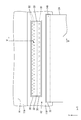
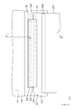
- Schematic plan view of a liquid crystal panel Schematic sectional view showing the sectional structure of the liquid crystal panel
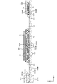
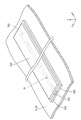
- An enlarged plan view of the non-display area of the LCD panel FIG. 4 is a cross-sectional view taken along the line VV in FIG. 4 and is an enlarged cross-sectional view of a non-display area of the liquid crystal panel Perspective view of the vicinity of the IC chip mounting area FIG.
- FIG. 4 is a cross-sectional view of a cross section of an IC chip cut along a short side direction, showing a shrinkage mode of ACF during curing shrinkage
- FIG. 9 is a cross-sectional view taken along the line XX in FIG. 9 and is an enlarged cross-sectional view of a non-display area of the liquid crystal panel
- FIG. 11 is a cross-sectional view taken along the line XII-XII in FIG.
- FIG. 11 is an enlarged cross-sectional view of a non-display area of the liquid crystal panel
- FIG. 14 is a sectional view taken along the line XV-XV in FIG.
- Embodiment 1 will be described with reference to the drawings.
- a liquid crystal display device (an example of a display device) 10 including a liquid crystal panel (an example of a display panel) 11 is illustrated.
- a part of each drawing shows an X-axis, a Y-axis, and a Z-axis, and each axis direction is drawn in a common direction in each drawing.
- the upper side of the figure is the front side and the lower side of the figure is the back side with reference to FIG.
- the liquid crystal display device 10 includes a liquid crystal panel 11, an IC chip 20 that is an electronic component that is mounted on the liquid crystal panel 11 and drives the liquid crystal panel 11, and the IC chip 20.
- a backlight device external light source for supplying light to the liquid crystal panel 11
- the liquid crystal display device 10 includes front and back external members 15 and 16 for housing and holding the liquid crystal panel 11 and the backlight device 14 assembled to each other.
- An opening 15A for visually recognizing an image displayed on the liquid crystal panel 11 is provided.
- the backlight device 14 includes a chassis 14A having a substantially box shape that opens toward the front side, and a light source (cold cathode tube, LED, organic EL, etc.) not shown disposed in the chassis 14A. And an optical member (not shown) arranged so as to cover the opening of the chassis 14A.
- the optical member has a function of converting light emitted from the light source into planar light. The light that has been planarized through the optical member is incident on the liquid crystal panel 11 and is used to display an image on the liquid crystal panel 11.
- the liquid crystal panel 11 has a vertically long rectangular shape as a whole, and the long side direction coincides with the Y-axis direction of each drawing, and the short side direction corresponds to the X-axis direction of each drawing. Match.
- a display area A1 capable of displaying an image is arranged on the majority thereof, and no image is displayed at a position biased to one end side (the lower side in FIG. 2) in the long side direction.
- Area A2 is arranged.
- the IC chip 20 and the flexible substrate 24 are mounted by pressure-bonding via an anisotropic conductive film (hereinafter referred to as “ACF”) 30 (see FIG. 4).
- ACF anisotropic conductive film
- a frame-shaped one-dot chain line that is slightly smaller than a color filter substrate 11A described later forms an outer shape of the display area A1, and an area outside the one-dot chain line is an area outside the one-dot chain line. It is a non-display area A2.
- the liquid crystal panel 11 includes a pair of glass substrates 11A and 11B having excellent translucency, and a liquid crystal layer 11C including liquid crystal molecules that are substances whose optical characteristics change with application of an electric field. It is equipped with. Both the substrates 11A and 11B constituting the liquid crystal panel 11 are bonded together by a sealing material (not shown) while maintaining a cell gap corresponding to the thickness of the liquid crystal layer 11C.
- the front side (front side) substrate 11A is a color filter substrate 11A
- the back side (back side) substrate 11B is an array substrate (an example of a circuit board) 11B.
- Alignment films 11D and 11E for aligning liquid crystal molecules contained in the liquid crystal layer 11C are formed on the inner surfaces of both the substrates 11A and 11B, respectively. Further, polarizing plates 11F and 11G are attached to the outer surface sides of the glass substrates 11A1 and 11B1 constituting both the substrates 11A and 11B, respectively.
- the color filter substrate 11A has a short side dimension substantially the same as that of the array substrate 11B, but has a long side dimension smaller than that of the array substrate 11B.
- the mounting area for the IC chip 20 and the flexible substrate 24 is secured here.
- the glass substrate 11B1 constituting the array substrate 11B has a color filter substrate 11A and a polarizing plate 11G bonded to the main part thereof, and the portions where the mounting areas of the IC chip 20 and the flexible substrate 24 are secured are the color filter substrate 11A and the glass substrate 11B1. It is not superimposed on the polarizing plate 11G.
- a large number of TFTs 17 and pixel electrodes 18 that are switching elements are arranged in a matrix. Is provided.
- a gate wiring (not shown) and a source wiring (not shown) having a lattice shape are disposed so as to surround the TFT 17 and the pixel electrode 18.
- the TFTs 17 and the pixel electrodes 18 are arranged in parallel in a matrix form at the intersections of the gate wirings and the source wirings that form a grid.
- the gate wiring and the source wiring are respectively connected to the gate electrode and the source electrode of the TFT 17, and the pixel electrode 18 is connected to the drain electrode of the TFT 17.
- the pixel electrode 18 has a vertically long rectangular shape when seen in a plan view, and is made of a transparent electrode material such as ITO (Indium Tin Oxide) or ZnO (Zinc Oxide).
- the array electrode 11B can be provided with a capacitor wiring (not shown) that is parallel to the gate wiring and crosses the pixel electrode 18.
- each colored portion such as R (red), G (green), B (blue), etc.
- a large number of color filters 11H are arranged in parallel so as to overlap each pixel electrode 18 on the array substrate 11B side in a plan view.
- a substantially lattice-shaped light shielding layer (black matrix) 11I for preventing color mixing is formed between the colored portions constituting the color filter 11H.
- the light shielding layer 11I is configured to overlap the above-described gate wiring and source wiring in a plan view.
- one display pixel as a display unit is configured by a set of three colored portions of R (red), G (green), and B (blue) and three pixel electrodes 18 facing the colored portions. Yes.
- the display pixel includes a red pixel having an R colored portion, a green pixel having a G colored portion, and a blue pixel having a B colored portion.
- the pixels of each color constitute a pixel group by being repeatedly arranged along the row direction (X-axis direction) on the plate surface of the liquid crystal panel 11, and this pixel group constitutes the column direction (Y-axis direction). Many are arranged side by side.
- the control board 22 is attached to the back surface of the chassis 14 ⁇ / b> A (the outer surface opposite to the liquid crystal panel 11 side) of the backlight device 14 with screws or the like.
- the control board 22 has electronic parts for supplying various input signals to the IC chip 20 mounted on a board made of paper phenol or glass epoxy resin, and has a wiring (conductive path) of a predetermined pattern (not shown). Routed formation.
- One end (one end side) of the flexible substrate 24 is electrically and mechanically connected to the control substrate 22 via the ACF 30.
- the flexible substrate 24 includes a base material made of a synthetic resin material (polyimide resin or the like) having insulation and flexibility, and a plurality of wiring patterns (not shown) on the base material. have.
- the flexible substrate 24 is connected to the control substrate 22 disposed on the back surface side of the chassis 14A as described above, while the one end portion 24A in the length direction is connected to the other end portion (the other end side).
- 24 ⁇ / b> B is connected to the other end of the liquid crystal panel 11 in the long side direction of the array substrate 11 ⁇ / b> B, and is bent back so that the cross-sectional shape is substantially U-shaped in the liquid crystal display device 10.
- Both end portions 24A and 24B in the length direction of the flexible substrate 24 form terminal portions (not shown) with the wiring pattern exposed to the outside, and these terminal portions are connected to the control substrate 22 and the liquid crystal panel 11, respectively. Are electrically connected to each other. As a result, an input signal supplied from the control board 22 side can be transmitted to the liquid crystal panel 11 side.
- the IC chip 20 has a drive circuit inside, and is formed by forming wirings and elements on a silicon wafer containing silicon with high purity.
- the IC chip 20 generates an output signal based on a signal supplied from the control board 22 which is a signal supply source, and outputs the output signal toward the display area A1 of the liquid crystal panel 11.
- the IC chip 20 has a horizontally long rectangular shape in plan view, the long side direction is along the short side direction of the liquid crystal panel 11, and the short side direction is the long side of the liquid crystal panel 11. It is arranged in a posture along the side direction.
- the IC chip 20 is directly mounted on the non-display area A2 of the array substrate 11B in the liquid crystal panel 11, that is, COG mounted.
- the flexible substrate 24 has a length direction along the long side direction (Y-axis direction) of the array substrate 11B, and the other end portion 24B is substantially the center of the other end portion in the long side direction of the array substrate 11B. Connected to the part. As shown in FIG. 4, the other end 24B of the flexible substrate 24 connected to the array substrate 11B extends along the short side direction (X-axis direction) of the array substrate 11B.
- the IC chip 20 is arranged at a position closer to the display area A1 than the flexible substrate 24 in a portion of the non-display area A2 of the array substrate 11B that does not overlap with the color filter substrate 11A. In other words, the IC chip 20 is arranged at a position sandwiched between the display area A1 and the flexible substrate 24 in the non-display area A2 of the array substrate 11B.
- an external connection terminal portion T1 for receiving an input signal from the flexible substrate 24 side is provided.
- the mounting area of the IC chip 20 on the array substrate 11B receives a panel-side input terminal T2 for supplying an input signal to the IC chip 20 and an output signal from the IC chip 20.
- the external connection terminal portion T1 and the panel side input terminal portion T2 are routed and formed so as to cross between the mounting area of the flexible substrate 24 and the mounting area of the IC chip 20 in the non-display area A2 of the array substrate 11B. Are electrically connected by relay wiring (not shown).
- the surface of a thin film made of the same metal material as the gate wiring or the source wiring is covered with the same transparent electrode material such as ITO and ZnO as the pixel electrode 18.
- a substrate-side terminal portion T4 is provided on one plate surface facing the array substrate 11B.
- the substrate side terminal portion T4 is electrically connected to the external connection terminal portion T1 via the ACF 30 disposed on the external connection terminal portion T1 of the array substrate 11B.
- the ACF 30 is composed of an insulating thermosetting resin 30A as an adhesive and a large number of conductive particles 30B dispersed and blended in the thermosetting resin 30A.
- the thermosetting resin 30A constituting the ACF 30 include a phenoxy resin and an epoxy resin to which a curing agent is added.
- the other end 24B of the flexible substrate 24 is crimped to the external connection terminal portion T1 of the array substrate 11B via the ACF 30, so that the external connection terminal portion T1 and the substrate side terminal portion T4 are The conductive particles 30B are sandwiched and crushed between the external connection terminal portions T1 and the substrate-side terminal portions T4.
- the two ends of the IC chip 20 in the short side direction are arranged on one surface (hereinafter referred to as “mounting surface”) 20A directed to the array substrate 11B side in plan view.
- a plurality of input-side bumps B1 and a plurality of output-side bumps B2 that form a rectangular shape and protrude in a block shape toward the array substrate 11B and are electrically connected to the IC chip 20 are provided.
- the plurality of input-side bumps B1 are arranged in a line at a predetermined pitch along the long side direction of the IC chip 20 so as to face the panel-side input terminal portion T2 of the array substrate 11B.
- the plurality of output-side bumps B2 are smaller in size in plan view than the input-side bumps B1, are opposed to the panel-side output terminal portion T3 of the array substrate 11B, are staggered at a predetermined pitch, and They are arranged in two rows.
- the input-side bump B1 of the IC chip 20 is electrically connected to the panel-side input terminal portion T2 via the ACF 30 disposed on the panel-side input terminal portion T2 of the array substrate 11B.
- the ACF 30 is interposed between the array substrate 11B and the IC chip 20 so as to cover the exposed surface of the panel side input terminal portion T2 and the exposed surface of the input side bump B1 without any gaps.
- the output-side bump B2 of the IC chip 20 is electrically connected to the panel-side output terminal portion T3 through the ACF 30 disposed on the panel-side output terminal portion T3 of the array substrate 11B.
- the ACF 30 is interposed between the array substrate 11B and the IC chip 20 so as to cover the exposed surface of the panel side output terminal portion T3 and the exposed surface of the output side bump B2 without any gaps.
- these two ACFs 30 are arranged along the long side direction of the mounting surface 20A of the IC chip 20 so as to be spaced apart from each other.
- the two ACFs 30 are arranged apart from each other in the direction (Y-axis direction) along the short side of the mounting surface 20A of the IC chip 20 (see FIGS. 4 to 6). ).
- These two ACFs 30 are arranged on the array substrate 11B in the same process in the manufacturing process of the liquid crystal panel 11, respectively.
- the two ACFs 30 are of the same type as the ACF 30 that electrically connects the external connection terminal portion T1 and the substrate side terminal portion T4, and the thermosetting resin 30A constituting the ACF 30 is the same.
- the type, and the type and content of the conductive particles 30B are all the same.
- the external connection terminal portion T1 and the board side terminal are also connected to the conduction mode between the panel side input terminal portion T2 and the input side bump B1 and the conduction mode between the panel side output terminal portion T3 and the output side bump B2. This is the same as the conduction mode between the portion T4.
- the IC chip 20 is pressure-bonded and connected to the array substrate 11B via the two ACFs 30 so that the panel-side input terminal portion T2 and the input-side bump B1 and the panel-side output terminal portion T3 and the output side are connected.
- the conductive particles 30B of the ACF 30 are sandwiched between the bumps B2 and crushed, and between the panel side input terminal portion T2 and the input side bump B1 and between the panel side output terminal portion T3 and the output side bump B2. Conduction between them is achieved.
- a resin film 32 is disposed between the array substrate 11B and the IC chip 20 so as to close a gap generated between the two ACFs 30. Accordingly, the portion facing the outside in the gap generated between the two ACFs 30 is closed by the resin film 32.
- the resin film 32 does not contain the conductive particles 30B like the ACF 30, and is composed of only a curable resin.
- the type of the curable resin, the type of the curing agent added to the curable resin, and the addition By adjusting the amount, the curing shrinkage rate is smaller than those of the two ACFs 30 described above.
- the resin film 32 is filled in a gap generated between the two ACFs 30 after the IC chip 20 is pressure-bonded and connected to the array substrate 11B via the two ACFs 30 in the manufacturing process of the liquid crystal panel 11. Is distributed.
- the resin film 32 is arranged so as to close the gap generated between the two ACFs 30, so that the resin film 32 is arranged between the center position of the IC chip 20 and the array substrate 11 ⁇ / b> B in a plan view. It has become. Also, as shown in FIG. 4, the two ACFs 30 and the resin film 32 interposed between the array substrate 11B and the IC chip 20 are both arranged so as to slightly protrude from the outer edge of the IC chip 20 in plan view. Yes. By doing this, even when the IC chip 20 is slightly shifted from the original mounting position when the IC chip 20 is mounted on the array substrate 11B in the manufacturing process of the liquid crystal panel 11, the array substrate 11B and the IC This is because good conduction with the chip 20 can be achieved.
- the IC chip 20 is connected to the array substrate 11B by the two ACFs 30, and these two ACFs 30 are arranged apart from each other.
- a resin film 32 is disposed so as to close a gap generated when the two ACFs 30 are separated from each other. Therefore, in the manufacturing process of the liquid crystal panel 11, when the two ACFs 30 interposed between the array substrate 11B and the IC chip 20 are cured and contracted, the ACF 30 causes the IC chip 20 to move toward the array substrate 11B along with the curing contraction of the ACF 30. The attractive force is alleviated in the region where the resin film 32 is disposed.
- FIG. 3 the warp amount of the IC chip 20 at the time of curing shrinkage of the ACF 30 is small, and the warp of the IC chip 20 can be suppressed as compared with the conventional configuration.
- the array substrate 11B Either the ACF 30 or the resin film 32 is interposed between the IC chip 20 and the portion facing the outside.
- the mounting area of the IC chip 20 on the array substrate 11B and the mounting surface 20A of the IC chip 20 That is, it is possible to prevent or suppress water or dust from entering the connection portion between the array substrate 11B and the IC chip 20.
- the IC chip 20 when the IC chip 20 has a rectangular shape in a plan view as in the present embodiment, the IC chip 20 is either one of the two ACFs 30 interposed between the array substrate 11B and the IC chip 20 during curing shrinkage. It tends to warp in the direction along the edge.
- the two ACFs 30 are arranged in a manner separated from each other in the direction along the end side forming the short side of the IC chip 20 having a rectangular shape in plan view.
- the resin film 32 is arranged so that the ACF 30 attracts the IC chip 20 to the array substrate 11B side as the ACF 30 is cured and contracted in the direction along the edge that makes the IC chip 20 warp easily. Relaxed in the area. As a result, the warp of the IC chip 20 can be effectively suppressed.
- the center position of the IC chip 20 in plan view is the position farthest from the four corners of the IC chip 20, so the center position and the array
- the IC chip 20 is easily warped when the ACF 30 is cured and contracted.
- the resin film 32 is disposed between the center position of the IC chip 20 in a plan view and the array substrate 11B. For this reason, the warp of the IC chip 20 can be effectively suppressed as compared with the configuration in which the center position is connected to the array substrate 11B by the ACF 30.
- a protrusion protruding toward the array substrate side is provided at a substantially central position of the mounting surface of the IC chip, and the tip surface of the protrusion is brought into contact with the array substrate, so that the array substrate and the IC chip It is possible to prevent or suppress the fluctuation of the distance between the two, and to suppress the warpage of the IC chip.
- providing such a protrusion on the IC chip mounting surface affects the IC chip mounting area on the array substrate and the circuit design provided on the IC chip mounting surface, and reduces the degree of freedom in circuit design. Problems arise.
- the provision of such a protrusion also causes a problem that the manufacturing cost of the IC chip increases.
- the warp of the IC chip 20 can be suppressed without providing such a protrusion, the above-described problem hardly occurs.
- FIG. 8 A modification of the first embodiment will be described with reference to FIG.
- the entire IC chip 120 is covered with a transparent sealing material 134, whereby the entire IC chip 120 is sealed with the sealing material 134. Since the other configuration is the same as that of the first embodiment, the description of the structure, operation, and effect is omitted.
- the part obtained by adding the numeral 100 to the reference numeral in FIG. 6 is the same as the part described in the first embodiment.
- the IC chip 120 is sealed by the sealing material 134 after the IC chip 120 is mounted on the array substrate 111B, that is, after the two ACFs 130 and the resin film 132 are cured. In this modification, the entire IC chip 120 is sealed in this way, so that further dustproof, moistureproof and waterproofing of the IC chip 120 can be achieved.
- the second embodiment will be described with reference to FIGS. 9 and 10.
- the second embodiment is different from the first embodiment in the arrangement of the ACF 230 that electrically connects the array substrate 211B and the flexible substrate 224. Since the other configuration is the same as that of the first embodiment, the description of the structure, operation, and effect is omitted.
- 9 and FIG. 10 the part obtained by adding the numeral 200 to the reference numerals in FIG. 4 and FIG. 5 is the same as the part described in the first embodiment.
- the ACF 230 that electrically connects the array substrate 211B and the flexible substrate 224 is input to the panel side input terminal portion T2 of the array substrate 211B and the IC chip 220.
- the ACF 230 is also used to electrically connect the side bump B1. That is, of the two ACFs 230 that connect between the array substrate 211B and the IC chip 220, the ACF 230 disposed near the flexible substrate 224 includes the external connection terminal portion T1 of the array substrate 211B and the substrate side terminal portion of the flexible substrate 224.
- the array substrate 211B and the flexible substrate 224 are electrically connected to each other up to T4.
- thermosetting resin constituting the ACF 230 is insulative, current does not flow directly from the substrate side terminal portion T4 of the flexible substrate 224 to the panel side input terminal portion T2 of the array substrate 211B through the ACF 230. Similar to the first embodiment, the panel-side input terminal portion of the array substrate 211B is connected through a relay wiring that is wired between the external connection terminal portion T1 and the panel-side input terminal portion T2 from the substrate-side terminal portion T4 of the flexible substrate 224. The current flows up to T2.
- the configuration as described above allows electrical connection between the panel-side input terminal portion T2 of the array substrate 211B and the input-side bump B1 of the IC chip 220 in the manufacturing process of the liquid crystal panel.
- the ACF 230 for connection, it is not necessary to separately provide an ACF for electrically connecting the array substrate 211B and the flexible substrate 224, so that the manufacturing process can be simplified.
- the third embodiment will be described with reference to FIGS. 11 and 12.
- the number of ACFs 330 interposed between the array substrate 311B and the IC chip 320 is different from that in the first embodiment. Since the other configuration is the same as that of the first embodiment, the description of the structure, operation, and effect is omitted.
- the parts obtained by adding the numeral 300 to the reference numerals in FIGS. 4 and 5 are the same as the parts described in the first embodiment.
- three ACFs 330 are interposed between the array substrate 311B and the IC chip 320. That is, the ACF 330 that electrically connects the panel side input terminal portion T2 of the array substrate 311B and the input side bump B1 of the IC chip 320, and the panel side input terminal portion T2 of the array substrate 311B and the input side bump B1 of the IC chip 320.
- ACF 330 that is electrically connected to each other is configured and arranged in the same manner as in the first embodiment, and one ACF 330 is arranged in a gap between the two ACFs 330 so as to be separated from the two ACFs 330. ing.
- One ACF 330 disposed between the two ACFs 330 is disposed along the long side direction of the mounting surface 320 ⁇ / b> A of the IC chip 320, similarly to the other two ACFs 330.
- the three ACFs 330 interposed between the array substrate 311B and the IC chip 320 are of the same type.
- the ACF 330 is connected to the IC along with the curing contraction of the ACF 330.
- the force that attracts the chip 320 to the array substrate 311B side is alleviated in the region where each resin film 332 is disposed.
- the curing shrinkage of the ACF 330 is smaller than that in the conventional configuration in which the IC chip is electrically connected to the array substrate through a single ACF.
- the amount of warping of the IC chip 320 at that time is small, and the warping of the IC chip 320 can be suppressed as compared with the conventional configuration.
- Embodiment 4 will be described with reference to FIG.
- the number of ACFs 430 interposed between the array substrate 411B and the IC chip 420 is different from that in the first embodiment. Since the other configuration is the same as that of the first embodiment, the description of the structure, operation, and effect is omitted.
- FIG. 13 a part obtained by adding a numeral 400 to the reference numeral in FIG. 4 is the same as the part described in the first embodiment.
- the input-side bump B1 provided side by side along the long side direction of the IC chip 420 on the mounting surface 420A of the IC chip 420 has a large gap at a substantially central position in the long side direction of the IC chip 420. It is arranged with a gap. That is, the input-side bump B1 is provided so as to be divided into two regions across the gap.
- the resin film 432 is disposed in the gap where the input-side bump B1 is not provided, and the ACF 430 is disposed in each of the two regions where the input-side bump B1 is provided.
- the output-side bump B2 provided side by side along the long side direction of the IC chip 420 on the mounting surface 420A of the IC chip 420 is a bump provided at a substantially central position in the long side direction of the IC chip 420.
- the dummy bump B3 is not electrically connected to the IC chip 420. That is, the output-side bump B2 is provided in a form divided into two regions with the dummy bump B3 interposed therebetween.
- the resin film 432 is disposed in the region where the dummy bump B3 is provided, and the ACF 430 is disposed in each of the two regions where the output-side bump B2 is provided.
- the four ACFs 430 overlap the four corners of the mounting surface 420A of the IC chip 420 in plan view.
- a substantially cross-shaped gap is formed between the four ACFs 430 in plan view.
- the four ACFs 430 are in the direction along the short side (Y-axis direction) and the direction along the long side (X-axis direction) of the mounting surface 420A of the IC chip 420. They are arranged so as to be separated from each other.
- a resin film 432 is disposed so as to close the substantially cross-shaped gap.
- the force by which the ACF 430 attracts the IC chip 420 toward the array substrate 411B as the ACF 430 is cured and contracted is relaxed in the region where the resin film 432 is disposed.
- the dummy bump B3 provided between the output-side bumps B2 is made of metal so that the heat dissipation of the IC chip 420 is improved, and the tip of the dummy bump B3 is in contact with the array substrate 411B. It functions to adjust the position of the IC chip 420 with respect to 411B (the distance between the array substrate 411B and the IC chip 420). As described above, in the present embodiment, the array substrate 411B and the IC chip 420 are electrically connected in the region where the input-side bump B1 and the output-side bump B2 are provided, and the dummy bump B3 is provided in the region where the dummy bump B3 is provided. The warp of the IC chip 420 can be suppressed while ensuring the above function.
- the fifth embodiment will be described with reference to FIGS. 14 and 15.
- the fifth embodiment is different from the first embodiment in the type of resin film disposed in the gap between two ACFs 530 interposed between the array substrate 511B and the IC chip 520. Since the other configuration is the same as that of the first embodiment, the description of the structure, operation, and effect is omitted. 14 and 15, the parts obtained by adding the numeral 500 to the reference numerals in FIGS. 4 and 5 are the same as the parts described in the first embodiment.
- the gap between the two ACFs 530 arranged to cover the input side bump B1 and the output side bump B2 of the IC chip 520 is closed,
- ACF an example of a resin film
- the arrangement of the input-side bump B1, the output-side bump B2, and the two ACFs 530 is the same as that of the first embodiment.
- the other type of ACF 531 is composed of a thermosetting resin 531A and a large number of conductive particles 531B dispersed and blended in the thermosetting resin 531A.
- the type of the curable resin 531A, the type of the curing agent added to the thermosetting resin 531A, and the amount added are different from those of the two ACFs 530.
- the two ACFs 530 and the other types of ACFs 531 can be arranged on the array substrate 511B in the same process in the manufacturing process of the liquid crystal panel. For this reason, a manufacturing process can be shortened compared with the case where a resin film is disposed between the two ACFs 530 by filling or the like after the IC chip 520 is connected to the array substrate 511B.
- the resin film disposed between adjacent ACFs is an example of an intermembrane member, and the resin disposed in a portion of the resin film excluding the portion facing the outside.
- membrane is an example of a low shrinkage
- Embodiment 6 will be described with reference to FIG.
- the sixth embodiment is different from the first embodiment in that an internal space S1 is provided in a part between the array substrate 611B and the IC chip 620. Since the other configuration is the same as that of the first embodiment, the description of the structure, operation, and effect is omitted.
- FIG. 16 the part obtained by adding the numeral 600 to the reference sign in FIG. 6 is the same as the part described in the first embodiment.
- the resin film 632 is formed in such a manner that only a portion facing the outside of the gap generated between the two ACFs 630 between the array substrate 611 ⁇ / b> B and the IC chip 620 is closed. Is arranged. That is, an internal space (an example of a low shrinkage ratio portion) S1 is provided between the array substrate 611B and the IC chip 620.
- the materials of each ACF 630 and each resin film 632 are the same as those in the first embodiment, and each resin film 632 is smaller in curing shrinkage than each ACF 630. Since the internal space S1 is filled with air, it is natural that the curing shrinkage rate in the internal space S1 is smaller than that of each ACF 630.
- a combination of the resin film 632 and the internal space S1 is an example of an intermembrane member.
- the ACF 630 is cured and contracted.
- the force that the ACF 630 attracts the IC chip 620 toward the array substrate 611B is relaxed in the internal space S1 and also in the region where the resin film 632 is disposed.
- the curing shrinkage of the ACF 630 as compared with the conventional configuration in which the IC chip is electrically connected to the array substrate through a single ACF.
- the amount of warping of the IC chip 620 at the time is small, and the warping of the IC chip 620 can be suppressed as compared with the conventional configuration.
- the portion facing the outside of the gap generated between the two ACFs 630 between the array substrate 611B and the IC chip 620 is closed by the resin film 632, and thus the array substrate 611B Either the ACF 630 or the resin film 632 is interposed in a portion facing the outside between the IC chip 620, and between the mounting area of the IC chip 620 on the array substrate 611B and the mounting surface 620A of the IC chip 620, That is, it is possible to prevent or suppress water, dust, or the like from entering the connection portion between the array substrate 611B and the IC chip 620.
- dust and moisture proofing of the connection portion between the array substrate 611B and the IC chip 620 is suppressed while suppressing the warp of the IC chip 620 electrically connected to the array substrate 611B via the ACF 630. And waterproofing can be aimed at.
- the plurality of ACFs interposed between the array substrate and the IC chip are arranged in a manner spaced apart from each other in the direction along one of the edges of the mounting surface of the IC chip.
- the configuration is not limited to this. If conduction between the array substrate and the IC chip can be achieved, a plurality of ACFs interposed between the array substrate and the IC chip are separated from each other in a direction that does not extend along one edge of the mounting surface of the IC chip. It may be a configuration arranged in the form.
- the arrangement of the plurality of ACFs arranged between the array substrate and the IC chip can be changed as appropriate.
- the array substrate constituting the liquid crystal panel is illustrated as an example of the circuit substrate, but the present invention is not limited to this.
- the present invention can be applied to various circuit boards on which electronic components are mounted on the board via the ACF.
- each resin film is smaller in curing shrinkage than each ACF.
- the internal space between the two ACFs with respect to the resin film is reduced. If the ratio is sufficiently large, each resin film may have a curing shrinkage rate larger than each ACF. Even in this case, when the effect of the two ACFs contracts, the force that the ACF attracts the IC chip toward the array substrate is alleviated by the internal space, so that the warpage of the IC chip can be suppressed compared to the conventional configuration. it can.
- SYMBOLS 10 Liquid crystal display device, 11 ... Liquid crystal panel, 11A ... Color filter substrate, 11A1, 11B1 ... Glass substrate, 11B, 111B, 211B, 311B, 411B, 511B, 611B ... Array substrate , 14 ... Backlight device, 20, 120, 220, 320, 420, 520, 620 ... IC chip, 22 ... Control board, 24, 224, 324, 424, 524 ... Flexible board, 30, 130, 230, 330, 430, 530, 531, 631... ACF, 32, 132, 232, 332, 432, 632 ... resin film (intermembrane member), 134 ...
Landscapes
- Engineering & Computer Science (AREA)
- Physics & Mathematics (AREA)
- Microelectronics & Electronic Packaging (AREA)
- Nonlinear Science (AREA)
- Chemical & Material Sciences (AREA)
- Manufacturing & Machinery (AREA)
- Crystallography & Structural Chemistry (AREA)
- General Physics & Mathematics (AREA)
- Optics & Photonics (AREA)
- Mathematical Physics (AREA)
- Ceramic Engineering (AREA)
- Inorganic Chemistry (AREA)
- Liquid Crystal (AREA)
- Wire Bonding (AREA)
- Devices For Indicating Variable Information By Combining Individual Elements (AREA)
Abstract
アレイ基板11Bは、アレイ基板11Bを構成するガラス基板と、ガラス基板上に配されたICチップ20と、ガラス基板と1つのICチップ20との間に介在して両者を電気的に接続する2つのACF30であって、互いに離間した形で配された2つのACF30と、ガラス基板と1つのICチップ20との間において隣り合うACF30の間に生じる隙間を塞ぐ形で配され、ACF30よりも硬化収縮率が小さい樹脂材料からなる樹脂膜32と、を備える。
Description
本発明は、回路基板、表示パネル及び表示装置に関する。
従来、絶縁性の接着剤の内部に導電性粒子が含有された異方性導電膜(ACF:Anisotropic Conductive Film)を介して、基板上にIC(Integrated Circuit)チップ等の電子部品が接続された回路基板が知られている。例えば、液晶パネル等の表示パネルでは、異方性導電膜を介して表示パネルを駆動するためのICチップを、表示パネルを構成するガラス基板上に接続する方法として、ICチップを表示パネルのうち表示領域外の領域に直接実装する、COG(Chip On Glass)実装技術が知られている。
上記COG実装では、通常、ガラス基板とICチップとの間に単一の異方性導電膜が配され、この異方性導電膜を介してガラス基板上にICチップが圧着接続される。また、異方性導電膜では、接着剤として熱硬化性樹脂が用いられる。このため、異方性導電膜の硬化収縮時に、異方性導電膜の硬化収縮に伴ってICチップがガラス基板側に引き付けられ、ICチップが反ってしまうことがある。このような異方性導電膜の硬化収縮時におけるICチップの反りを低減させる技術が、例えば特許文献1に開示されている。
(発明が解決しようとする課題)
ところで、上記のような回路基板においては、基板上の電子部品が配される領域、及び電子部品における基板と対向する面にそれぞれ接続端子が設けられるため、基板と電子部品との接続箇所に水や塵等が浸入することを防止ないし抑制することが要求される。このため、上記のような回路基板では、基板上に配される電子部品の反りを低減させることに加えて基板と電子部品との接続箇所の防塵、防湿及び防水を図ることが要求される。
ところで、上記のような回路基板においては、基板上の電子部品が配される領域、及び電子部品における基板と対向する面にそれぞれ接続端子が設けられるため、基板と電子部品との接続箇所に水や塵等が浸入することを防止ないし抑制することが要求される。このため、上記のような回路基板では、基板上に配される電子部品の反りを低減させることに加えて基板と電子部品との接続箇所の防塵、防湿及び防水を図ることが要求される。
本明細書で開示される技術は、上記の課題に鑑みて創作されたものであって、異方性導電膜を介して基板と電気的に接続される電子部品の反りを抑制しながら、基板と電子部品との接続箇所の防塵、防湿及び防水を図ることを目的とする。
(課題を解決するための手段)
本明細書で開示される技術は、基板と、前記基板上に配された電子部品と、前記基板と1つの前記電子部品との間に介在して両者を電気的に接続する複数の異方性導電膜であって、互いに離間した形で配された複数の異方性導電膜と、前記基板と1つの前記電子部品との間において隣り合う前記異方性導電膜の間に生じる隙間に配され、該隙間の少なくとも外部に臨む部位を塞ぐ形で配された少なくとも一つの樹脂膜と、前記異方性導電膜よりも硬化収縮率が小さい低収縮率部と、を有する膜間部材と、を備える回路基板に関する。
本明細書で開示される技術は、基板と、前記基板上に配された電子部品と、前記基板と1つの前記電子部品との間に介在して両者を電気的に接続する複数の異方性導電膜であって、互いに離間した形で配された複数の異方性導電膜と、前記基板と1つの前記電子部品との間において隣り合う前記異方性導電膜の間に生じる隙間に配され、該隙間の少なくとも外部に臨む部位を塞ぐ形で配された少なくとも一つの樹脂膜と、前記異方性導電膜よりも硬化収縮率が小さい低収縮率部と、を有する膜間部材と、を備える回路基板に関する。
上記の回路基板では、1つの電子部品が複数の異方性導電膜によって基板に接続され、各異方性導電膜が互いに離間した形で配されるとともに、離間することにより生じる隙間に膜間部材が配される。そしてこの膜間部材は、異方性導電膜よりも硬化収縮率が小さい低収縮率部を有している。このため、異方性導電膜の硬化収縮時に、異方性導電膜の硬化収縮に伴って異方性導電膜が電子部品を基板側に引き付ける力が、当該低収縮率部とされた領域において緩和される。その結果、基板と電子部品との間の異方性導電膜を配すべき領域において、電子部品が単一の異方性導電膜(離間した構成を有しない膜)を介して基板に電気的に接続される従来の構成と比べて電子部品の反りを抑制することができる。
また、膜間部材は複数の異方性導電膜の間に生じる隙間の少なくとも外部に臨む部位を塞ぐ形で配された樹脂膜を有しているので、当該部位が樹脂膜によって塞がれる。これにより、基板と電子部品との間における外部に臨む部位には異方性導電膜と樹脂膜とのいずれかが介在する形となり、基板と電子部品との接続箇所に水や塵等が浸入することを防止ないし抑制することができる。以上のように上記の回路基板では、異方性導電膜を介して基板と電気的に接続される電子部品の反りを抑制しながら、基板と電子部品との接続箇所の防塵、防湿及び防水を図ることができる。
前記樹脂膜と前記低収縮率部とが同一の材料で形成されていてもよい。
この構成によると、異方性導電膜の硬化収縮時に、異方性導電膜の硬化収縮に伴って異方性導電膜が電子部品を基板側に引き付ける力が、低収縮率部だけでなく、樹脂膜においても緩和される。このため、電子部品の反りを一層抑制することができる。
前記電子部品は平面視矩形状をなし、前記複数の異方性導電膜は、平面視矩形状の前記電子部品のいずれかの端辺に沿った方向において互いに離間した形で配されていてもよい。
電子部品が平面視矩形状である場合、当該電子部品は、基板と電子部品との間に介在する複数の異方性導電膜の硬化収縮時に、いずれかの端辺に沿った方向に反り易い。上記の構成によると、電子部品が反り易い上記いずれかの端辺に沿った方向において、異方性導電膜の硬化収縮に伴って異方性導電膜が電子部品を基板側に引き付ける力が、樹脂膜が配された領域において緩和される。その結果、電子部品の反りを効果的に抑制することができる。
平面視における前記電子部品の中心位置と前記基板との間に前記低収縮率部が配されていてもよい。
電子部品が平面視矩形状である場合、平面視における電子部品の中心位置は、電子部品の四隅から最も離れた位置であるので、当該中心位置と基板との間が異方性導電膜によって接続されていると、異方性導電膜の硬化収縮時に電子部品が大きく反り易い。上記の構成によると、上記中心位置と基板との間に上記低収縮率部が配されることで、当該中心位置が異方性導電膜によって基板に接続される構成と比べて、電子部品の反りを効果的に抑制することができる。
前記電子部品には、前記基板側に向かって突出するとともに前記電子部品と導通するバンプと、前記基板側に向かって突出するとともに前記電子部品と導通しないダミーバンプと、が設けられ、前記複数の異方性導電膜は少なくとも前記バンプが設けられた領域に配されていてもよい。
この構成によると、バンプが設けられた領域において基板と電子部品との間の導通を図るとともに、ダミーバンプが設けられた領域において電子部品の放熱性の向上や電子部品の位置の調整等、ダミーバンプとしての機能を確保しながら、電子部品の反りを抑制することができる。
前記電子部品が封止材で覆われていてもよい。
この構成によると、封止材によって電子部品の一層の防塵、防湿及び防水を図ることができる。
本明細書で開示される他の技術は、上記の回路基板を備える表示パネルであって、前記基板は、画像を表示する表示領域と画像を表示しない非表示領域とを有し、前記電子部品は、前記基板の前記非表示領域に配される表示パネルとして表現することもできる。
上記の表示パネルでは、前記基板の前記非表示領域に接続されたフレキシブル基板を備え、複数の前記異方性導電膜のうち一つの前記異方性導電膜が、前記基板と前記フレキシブル基板との間に至るまで延在して配されて該基板と該フレキシブル基板とを電気的に接続するものとされていてもよい。
この構成によると、表示パネルの製造過程において、基板とフレキシブル基板との間に両者を電気的に接続するための異方性導電膜を別途配する必要がないので、表示パネルの製造工程を簡略化することができる。
本明細書で開示される他の技術は、照明装置と、該照明装置からの光を利用して表示を行う上記の表示パネルと、を備え、前記電子部品は前記表示パネルを駆動するICチップである表示装置として表現することもできる。
(発明の効果)
本明細書で開示される技術によれば、異方性導電膜を介して基板と電気的に接続される電子部品の反りを抑制しながら、基板と電子部品との接続箇所の防塵、防湿及び防水を図ることができる。
本明細書で開示される技術によれば、異方性導電膜を介して基板と電気的に接続される電子部品の反りを抑制しながら、基板と電子部品との接続箇所の防塵、防湿及び防水を図ることができる。
<実施形態1>
図面を参照して実施形態1を説明する。本実施形態では、液晶パネル(表示パネルの一例)11を備える液晶表示装置(表示装置の一例)10について例示する。なお、各図面の一部にはX軸、Y軸およびZ軸を示しており、各軸方向が各図面で共通した方向となるように描かれている。また、上下方向については、図1を基準とし、同図上側を表側とするとともに同図下側を裏側とする。
図面を参照して実施形態1を説明する。本実施形態では、液晶パネル(表示パネルの一例)11を備える液晶表示装置(表示装置の一例)10について例示する。なお、各図面の一部にはX軸、Y軸およびZ軸を示しており、各軸方向が各図面で共通した方向となるように描かれている。また、上下方向については、図1を基準とし、同図上側を表側とするとともに同図下側を裏側とする。
液晶表示装置10は、図1及び図2に示すように、液晶パネル11と、液晶パネル11に実装されて当該液晶パネル11を駆動する電子部品であるICチップ20と、ICチップ20に対して各種入力信号を外部から供給するコントロール基板22と、液晶パネル11と外部のコントロール基板22とを電気的に接続するフレキシブル基板24と、液晶パネル11に光を供給する外部光源であるバックライト装置(照明装置の一例)14と、を備えている。また、液晶表示装置10は、相互に組み付けた液晶パネル11及びバックライト装置14を収容して保持するための表裏一体の外部部材15,16を備えており、このうち表側の外部部材15には、液晶パネル11に表示された画像を外部から視認させるための開口部15Aが設けられている。
先にバックライト装置14について簡単に説明する。バックライト装置14は、図1に示すように、表側に向けて開口した略箱型をなすシャーシ14Aと、シャーシ14A内に配された図示しない光源(冷陰極管、LED、有機EL等)と、シャーシ14Aの開口部を覆う形で配される図示しない光学部材と、を備えている。光学部材は、光源から出射される光を面状の光に変換する等の機能を有している。光学部材を通過して面状となった光は、液晶パネル11に入射し、液晶パネル11において画像を表示するために利用される。
次に、液晶パネル11について説明する。液晶パネル11は、図2に示すように、全体として縦長の矩形状をなしており、その長辺方向が各図面のY軸方向と一致し、その短辺方向が各図面のX軸方向と一致している。液晶パネル11では、その大部分に画像を表示可能な表示領域A1が配され、その長辺方向における一方の端部側(図2に示す下側)に偏った位置に画像が表示されない非表示領域A2が配されている。非表示領域A2の一部には、ICチップ20及びフレキシブル基板24が異方性導電膜(以下、「ACF」と称する)30(図4参照)を介した圧着接続によって実装されている。なお、液晶パネル11では、図1に示すように、後述するカラーフィルタ基板11Aよりも一回り小さな枠状の一点鎖線が表示領域A1の外形をなしており、当該一点鎖線よりも外側の領域が非表示領域A2となっている。
液晶パネル11は、図3に示すように、透光性に優れた一対のガラス製の基板11A、11Bと、電界印加に伴って光学特性が変化する物質である液晶分子を含む液晶層11Cと、を備えている。液晶パネル11を構成する両基板11A,11Bは、液晶層11Cの厚さ分のセルギャップを維持した状態で図示しないシール材によって貼り合わされている。両基板11A,11Bのうち、表側(正面側)の基板11Aがカラーフィルタ基板11Aとされ、裏側(背面側)の基板11Bがアレイ基板(回路基板の一例)11Bとされる。両基板11A,11Bの内面側には、液晶層11Cに含まれる液晶分子を配向させるための配向膜11D,11Eがそれぞれ形成されている。また、両基板11A,11Bを構成するガラス基板11A1,11B1の外面側には、それぞれ偏光板11F,11Gが貼り付けられている。
カラーフィルタ基板11Aは、図2に示すように、短辺寸法がアレイ基板11Bとほぼ同等であるものの、長辺寸法がアレイ基板11Bよりも小さく、アレイ基板11Bに対して長辺方向についての一方の端部(図2に示す上側)を揃えた状態で貼り合わされている。従って、アレイ基板11Bのうち長辺方向についての他方の端部(図1に示す下側)は、所定範囲に亘ってカラーフィルタ基板11Aが重なり合うことがなく、表裏両板面が外部に露出した状態とされており、ここにICチップ20及びフレキシブル基板24の実装領域が確保されている。アレイ基板11Bを構成するガラス基板11B1は、その主要部分にカラーフィルタ基板11A及び偏光板11Gが貼り合わされており、ICチップ20及びフレキシブル基板24の実装領域が確保された部分がカラーフィルタ基板11A及び偏光板11Gと非重畳とされている。
続いてアレイ基板11B及びカラーフィルタ基板11Aにおける表示領域A1内の構成について説明する。アレイ基板11Bを構成するガラス基板(基板の一例)11B1の内面側(液晶層11C側)には、図3に示すように、スイッチング素子であるTFT17及び画素電極18が多数個ずつマトリクス状に並んで設けられている。これらTFT17及び画素電極18の周りには、格子状をなす図示しないゲート配線及び図示しないソース配線が取り囲むようにして配設されている。換言すると、格子状をなすゲート配線及びソース配線の交差部に、TFT17及び画素電極18が行列状に並列配置されている。ゲート配線とソース配線はそれぞれTFT17のゲート電極とソース電極とに接続され、画素電極18がTFT17のドレイン電極に接続されている。また、画素電極18は、平面に視て縦長の矩形状をなすとともに、ITO(Indium Tin Oxide)、ZnO(Zinc Oxide)等の透明電極材料からなる。なお、アレイ電極11Bには、ゲート配線に並行するとともに画素電極18を横切る容量配線(不図示)を設けることも可能である。
一方、カラーフィルタ基板11Aを構成するガラス基板11A1の内面側(液晶層11C側)には、図3に示すように、R(赤色),G(緑色),B(青色)等の各着色部が、アレイ基板11B側の各画素電極18と平面に視て重畳するような多数個マトリクス状に並列して配置されたカラーフィルタ11Hが設けられている。カラーフィルタ11Hを構成する各着色部間には、混色を防ぐための略格子状の遮光層(ブラックマトリクス)11Iが形成されている。遮光層11Iは、上記したゲート配線及びソース配線と平面に視て重畳する構成とされる。カラーフィルタ11H及び遮光層11Iの表面には、アレイ基板11Bの画素電極18と対向するベタ状の対向電極11Jが設けられている。液晶パネル11では、R(赤色),G(緑色),B(青色)の3色の着色部及びそれらと対向する3つの画素電極18の組によって表示単位である1つの表示画素が構成されている。表示画素は、Rの着色部を有する赤色画素と、Gの着色部を有する緑色画素と、Bの着色部を有する青色画素とからなる。これら各色の画素は、液晶パネル11の板面において行方向(X軸方向)に沿って繰り返し並べて配されることで、画素群を構成しており、この画素群が列方向(Y軸方向)に沿って多数並んで配されている。
次に、液晶パネル11に接続される各部材について説明する。コントロール基板22は、図1及び図2に示すように、バックライト装置14におけるシャーシ14Aの裏面(液晶パネル11側とは反対側の外面)にネジ等によって取り付けられている。このコントロール基板22は、紙フェノール又はガラスエポキシ樹脂製の基板上に、ICチップ20に各種入力信号を供給するための電子部品が実装されるとともに、図示しない所定のパターンの配線(導電路)が配索形成されている。このコントロール基板22には、フレキシブル基板24の一方の端部(一端側)がACF30を介して電気的にかつ機械的に接続されている。
フレキシブル基板24は、図1に示すように、絶縁性及び可撓性を有する合成樹脂材料(ポリイミド系樹脂等)からなる基材を備え、その基材上に多数本の配線パターン(不図示)を有している。フレキシブル基板24は、長さ方向についての一方の端部24Aが既述したようにシャーシ14Aの裏面側に配されたコントロール基板22に接続されるのに対し、他方の端部(他端側)24Bが液晶パネル11におけるアレイ基板11Bの長辺方向についての他方の端部に接続されており、液晶表示装置10内で断面形状が略U字状となるように折り返し状に屈曲されている。フレキシブル基板24における長さ方向についての両端部24A,24Bは、配線パターンが外部に露出して端子部(不図示)を構成しており、これらの端子部がそれぞれコントロール基板22及び液晶パネル11に対して電気的に接続されている。これにより、コントロール基板22側から供給される入力信号を液晶パネル11側に伝送することが可能とされている。
ICチップ20は、内部に駆動回路を有しており、シリコンを高い純度で含んだシリコンウェハ上に配線や素子が形成されてなるものである。ICチップ20は、信号供給源であるコントロール基板22から供給される信号に基づいて出力信号を生成し、その出力信号を液晶パネル11の表示領域A1へ向けて出力する。ICチップ20は、図2に示すように、平面に視て横長の矩形状をなしており、その長辺方向が液晶パネル11の短辺方向に沿うとともにその短辺方向が液晶パネル11の長辺方向に沿った姿勢で配されている。このICチップ20は、液晶パネル11におけるアレイ基板11Bの非表示領域A2に対して直接実装、即ちCOG実装されている。
続いてアレイ基板11Bの非表示領域A2におけるフレキシブル基板24及びICチップ20の接続態様について詳しく説明する。フレキシブル基板24は、その長さ方向がアレイ基板11Bの長辺方向(Y軸方向)に沿った姿勢で、その他方の端部24Bがアレイ基板11Bの長辺方向について他方の端部の略中央部分に接続されている。アレイ基板11Bに接続されたフレキシブル基板24の他方の端部24Bは、図4に示すように、アレイ基板11Bの短辺方向(X軸方向)に沿って延在している。ICチップ20は、アレイ基板11Bにおける非表示領域A2のうちカラーフィルタ基板11Aと非重畳となる部分において、フレキシブル基板24よりも表示領域A1側寄りに位置して配されている。換言すれば、ICチップ20は、アレイ基板11Bの非表示領域A2のうち、表示領域A1とフレキシブル基板24との間に挟まれた位置に配されている。
アレイ基板11Bにおけるフレキシブル基板24の実装領域には、図5に示すように、フレキシブル基板24側から入力信号の供給を受けるための外部接続端子部T1が設けられている。一方、アレイ基板11BにおけるICチップ20の実装領域には、当該ICチップ20に対して入力信号の供給を図るためのパネル側入力端子部T2と、ICチップ20からの出力信号の供給を受けるためのパネル側出力端子部T3と、がそれぞれ設けられている。外部接続端子部T1とパネル側入力端子部T2とは、アレイ基板11Bの非表示領域A2のうち、フレキシブル基板24の実装領域とICチップ20の実装領域との間を横切る形で配索形成された中継配線(不図示)によって電気的に接続されている。パネル側入力端子部T2及びパネル側出力端子部T3は、ゲート配線又はソース配線と同じ金属材料からなる薄膜の表面が、画素電極18と同じITO、ZnO等の透明電極材料によって覆われている。
フレキシブル基板24の他方の端部24Bには、図5に示すように、アレイ基板11B側に向けられた一方の板面に基板側端子部T4が設けられている。基板側端子部T4は、アレイ基板11Bの外部接続端子部T1上に配されたACF30を介して当該外部接続端子部T1と電気的に接続されている。ACF30は、接着剤である絶縁性の熱硬化性樹脂30Aと、この熱硬化性樹脂30A中に分散配合された多数の導電性粒子30Bと、からなっている。ACF30を構成する熱硬化性樹脂30Aとしては、硬化剤が添加されたフェノキシ樹脂やエポキシ樹脂が挙げられる。本実施形態では、フレキシブル基板24の他方の端部24BがACF30を介してアレイ基板11Bの外部接続端子部T1に対して圧着接続されることで、外部接続端子部T1と基板側端子部T4との間に導電性粒子30Bが挟み込まれて押し潰され、これにより、外部接続端子部T1と基板側端子部T4との間で導通が図られるようになっている。
ICチップ20の短辺方向の両端部には、図4及び図5に示すように、アレイ基板11B側に向けられた一方の面(以下、「実装面」と称する)20Aに、それぞれ平面視矩形状をなしてアレイ基板11B側に向かってブロック状に突出するとともにICチップ20と導通する複数の入力側バンプB1と複数の出力側バンプB2とが設けられている。このうち複数の入力側バンプB1は、アレイ基板11Bのパネル側入力端子部T2と対向する形で、ICチップ20の長辺方向に沿って所定のピッチで一列に並んで設けられている。一方、複数の出力側バンプB2は、平面に視た大きさが入力側バンプB1より小さいものとされ、アレイ基板11Bのパネル側出力端子部T3と対向する形で、所定のピッチで互い違い状かつ二列に並んで設けられている。
ICチップ20の入力側バンプB1は、アレイ基板11Bのパネル側入力端子部T2に配されたACF30を介して当該パネル側入力端子部T2と電気的に接続されている。このACF30は、パネル側入力端子部T2の露出面と入力側バンプB1の露出面とをそれぞれ隙間無く覆う形でアレイ基板11BとICチップ20との間に介在している。一方、ICチップ20の出力側バンプB2は、アレイ基板11Bのパネル側出力端子部T3に配されたACF30を介して当該パネル側出力端子部T3と電気的に接続されている。このACF30は、パネル側出力端子部T3の露出面と出力側バンプB2の露出面とをそれぞれ隙間無く覆う形でアレイ基板11BとICチップ20との間に介在している。本実施形態においてこれら2つのACF30は、互いに離間した形で、それぞれICチップ20の実装面20Aの長辺方向に沿って配されている。換言すれば、2つのACF30は、ICチップ20の実装面20Aのうち短辺をなす端辺に沿った方向(Y軸方向)において互いに離間した形で配されている(図4乃至図6参照)。これら2つのACF30は、液晶パネル11の製造過程において、それぞれ同一の工程でアレイ基板11B上に配される。
なお、上記2つのACF30は、外部接続端子部T1と基板側端子部T4との間を電気的に接続するACF30と同一種類のものとされており、当該ACF30を構成する熱硬化性樹脂30Aの種類、及び導電性粒子30Bの種類、含有率はいずれも同一とされている。また、パネル側入力端子部T2と入力側バンプB1との間の導通態様、及びパネル側出力端子部T3と出力側バンプB2との間の導通態様についても、外部接続端子部T1と基板側端子部T4との間の導通態様と同一である。即ち、ICチップ20が上記2つのACF30を介してアレイ基板11B上に圧着接続されることで、パネル側入力端子部T2と入力側バンプB1との間、及びパネル側出力端子部T3と出力側バンプB2との間にACF30の導電性粒子30Bがそれぞれ挟み込まれて押し潰され、パネル側入力端子部T2と入力側バンプB1との間、及びパネル側出力端子部T3と出力側バンプB2との間の導通が図られている。
また、アレイ基板11BとICチップ20の間には、図4乃至図6に示すように、上記2つのACF30の間に生じる隙間を塞ぐ形で樹脂膜32が配されている。従って、2つのACF30の間に生じる隙間のうち外部に臨む部位は、この樹脂膜32によって塞がれた状態となっている。この樹脂膜32は、ACF30のように導電性粒子30Bを含有しておらず、硬化性樹脂のみで構成され、当該硬化性樹脂の種類や当該硬化性樹脂に添加される硬化剤の種類、添加量が調整されることで、上記2つのACF30よりも硬化収縮率が小さいものとされている。また、この樹脂膜32は、液晶パネル11の製造過程において、ICチップ20が上記2つのACF30を介してアレイ基板11B上に圧着接続された後に、上記2つのACF30の間に生じる隙間に充填されることで配されている。
なお、樹脂膜32が上記2つのACF30の間に生じる隙間を塞ぐ形で配されることで、平面視におけるICチップ20の中心位置とアレイ基板11Bとの間に樹脂膜32が配された形となっている。また、図4に示すように、アレイ基板11BとICチップ20との間に介在する2つのACF30及び樹脂膜32はいずれも、平面視においてICチップ20の外縁からわずかにはみ出す形で配されている。こうすることで、液晶パネル11の製造過程において、アレイ基板11B上へのICチップ20の実装時に、ICチップ20が本来の実装位置からわずかにずれた場合であっても、アレイ基板11BとICチップ20との間の良好な導通が図れるからである。
ところで、液晶パネルの製造過程においてアレイ基板上にICチップをCOG実装する際には、通常、アレイ基板とICチップとの間に単一のACFが配され、当該ACFを介してアレイ基板上にICチップが圧着接続される。このため、従来の液晶パネルの製造過程では、ACFの硬化収縮時に、ACFの硬化収縮に伴ってICチップの実装面のうちACFを配すべき領域の全域がACFによってアレイ基板側に引き付けられ、ICチップが大きく反ってしまうことがあった。このようにICチップが大きく反ってしまうと、アレイ基板とICチップとの間で良好な接続状態を確保できないことがあった。
これに対し本実施形態では、上述したように、ICチップ20が2つのACF30によってアレイ基板11Bに接続され、これら2つのACF30が互いに離間した形で配されている。そして、2つのACF30が離間することにより生じる隙間を塞ぐ形で樹脂膜32が配されている。このため、液晶パネル11の製造工程において、アレイ基板11BとICチップ20との間に介在する2つのACF30の硬化収縮時に、ACF30の硬化収縮に伴ってACF30がICチップ20をアレイ基板11B側に引き付ける力が、当該樹脂膜32が配された領域において緩和される。その結果、アレイ基板11BとICチップ20との間のACF30を配すべき領域において、ICチップが単一のACFを介してアレイ基板に電気的に接続される従来の構成と比べて、図7に示すように、ACF30の硬化収縮時におけるICチップ20の反り量が小さいものとなり、従来の構成と比べてICチップ20の反りを抑制することができる。
さらに本実施形態では、上述したように、アレイ基板11BとICチップ20との間において2つのACF30の間に生じる隙間のうち外部に臨む部位が樹脂膜32によって塞がれるので、アレイ基板11BとICチップ20との間における外部に臨む部位にはACF30と樹脂膜32とのいずれかが介在する形となり、アレイ基板11BにおけるICチップ20の実装領域とICチップ20の実装面20Aとの間、即ちアレイ基板11BとICチップ20との接続箇所に水や塵等が浸入することを防止ないし抑制することができる。このように本実施形態の液晶パネル11では、ACF30を介してアレイ基板11Bと電気的に接続されるICチップ20の反りを抑制しながら、アレイ基板11BとICチップ20との接続箇所の防塵、防湿及び防水を図ることができる。
ここで本実施形態のようにICチップ20が平面視矩形状である場合、当該ICチップ20は、アレイ基板11BとICチップ20との間に介在する2つのACF30の硬化収縮時に、いずれかの端辺に沿った方向に反り易い。この点、本実施形態では、2つのACF30が、平面視矩形状をなすICチップ20の短辺をなす端辺に沿った方向において互いに離間した形で配されている。このため、ICチップ20が反り易い上記辺をなす端辺に沿った方向において、ACF30の硬化収縮に伴ってACF30がICチップ20をアレイ基板11B側に引き付ける力が、樹脂膜32が配された領域において緩和される。その結果、ICチップ20の反りを効果的に抑制することができる。
また、本実施形態のようにICチップ20が平面視矩形状である場合、平面視におけるICチップ20の中心位置は、ICチップ20の四隅から最も離れた位置であるので、当該中心位置とアレイ基板11Bとの間がACF30によって接続されていると、ACF30の硬化収縮時にICチップ20が大きく反り易い。この点、本実施形態では、平面視におけるICチップ20の中心位置とアレイ基板11Bとの間に樹脂膜32が配されている。このため、当該中心位置がACF30によってアレイ基板11Bに接続される構成と比べて、ICチップ20の反りを効果的に抑制することができる。
なお、ICチップの実装面の略中央位置にアレイ基板側に向かって突出する突起を設け、その突起の先端面をアレイ基板と当接させることで、当該略中央位置においてアレイ基板とICチップとの間の距離が変動することを防止ないし抑制でき、ICチップの反りを抑制することもできる。しかしながら、ICチップの実装面にこのような突起を設けると、アレイ基板におけるICチップの実装領域やICチップの実装面に設けられる回路の設計に影響を与え、回路設計の自由度が減ってしまう問題が生じる。また、このような突起を設けることでICチップの製造コストが増加する問題も生じる。これに対し本実施形態では、このような突起を設けることなくICチップ20の反りを抑制することができるので、上記のような問題は生じ難い。
<実施形態1の変形例>
図8を参照して実施形態1の変形例を説明する。本変形例では、図8に示すように、ICチップ120の全体が透明な封止材134によって覆われており、これにより、ICチップ120の全体が封止材134によって封止されている。その他の構成については実施形態1と同様であるため、構造、作用、及び効果の説明は省略する。なお、図8において、図6の参照符号に数字100を加えた部位は、実施形態1で説明した部位と同一である。本変形例では、液晶パネルの製造工程において、アレイ基板111Bに対するICチップ120の実装後、即ち2つのACF130及び樹脂膜132の硬化後に、封止材134によってICチップ120を封止する。本変形例では、このようにICチップ120の全体が封止されることで、ICチップ120の一層の防塵、防湿及び防水を図ることができる。
図8を参照して実施形態1の変形例を説明する。本変形例では、図8に示すように、ICチップ120の全体が透明な封止材134によって覆われており、これにより、ICチップ120の全体が封止材134によって封止されている。その他の構成については実施形態1と同様であるため、構造、作用、及び効果の説明は省略する。なお、図8において、図6の参照符号に数字100を加えた部位は、実施形態1で説明した部位と同一である。本変形例では、液晶パネルの製造工程において、アレイ基板111Bに対するICチップ120の実装後、即ち2つのACF130及び樹脂膜132の硬化後に、封止材134によってICチップ120を封止する。本変形例では、このようにICチップ120の全体が封止されることで、ICチップ120の一層の防塵、防湿及び防水を図ることができる。
<実施形態2>
図9及び図10を参照して実施形態2を説明する。実施形態2は、アレイ基板211Bとフレキシブル基板224との間を電気的に接続するACF230の配置態様が実施形態1のものと異なっている。その他の構成については実施形態1と同様であるため、構造、作用、及び効果の説明は省略する。なお、図9及び図10において、それぞれ図4及び図5の参照符号に数字200を加えた部位は、実施形態1で説明した部位と同一である。
図9及び図10を参照して実施形態2を説明する。実施形態2は、アレイ基板211Bとフレキシブル基板224との間を電気的に接続するACF230の配置態様が実施形態1のものと異なっている。その他の構成については実施形態1と同様であるため、構造、作用、及び効果の説明は省略する。なお、図9及び図10において、それぞれ図4及び図5の参照符号に数字200を加えた部位は、実施形態1で説明した部位と同一である。
本実施形態では、図9及び図10に示すように、アレイ基板211Bとフレキシブル基板224との間を電気的に接続するACF230が、アレイ基板211Bのパネル側入力端子部T2とICチップ220の入力側バンプB1との間を電気的に接続するためのACF230を兼用するものとされている。即ち、アレイ基板211BとICチップ220との間を接続する2つのACF230のうち、フレキシブル基板224寄りに配されたACF230が、アレイ基板211Bの外部接続端子部T1とフレキシブル基板224の基板側端子部T4との間に至るまで配されてアレイ基板211Bとフレキシブル基板224とを電気的に接続するものとされている。なお、ACF230を構成する熱硬化性樹脂は絶縁性とされているから、フレキシブル基板224の基板側端子部T4からACF230を通じてアレイ基板211Bのパネル側入力端子部T2まで直接電流が流れるのではなく、実施形態1と同様に、フレキシブル基板224の基板側端子部T4から外部接続端子部T1とパネル側入力端子部T2との間に配索形成された中継配線を通じてアレイ基板211Bのパネル側入力端子部T2まで電流が流れるようになっている。
本実施形態では、上記のような構成とされていることで、液晶パネルの製造過程において、アレイ基板211Bのパネル側入力端子部T2とICチップ220の入力側バンプB1との間を電気的に接続するためのACF230に加えて、アレイ基板211Bとフレキシブル基板224との間を電気的に接続するためのACFを別途配する必要がないので、製造工程を簡略化することができる。
<実施形態3>
図11及び図12を参照して実施形態3を説明する。実施形態3は、アレイ基板311BとICチップ320との間に介在するACF330の数が実施形態1のものと異なっている。その他の構成については実施形態1と同様であるため、構造、作用、及び効果の説明は省略する。なお、図11及び図12において、それぞれ図4及び図5の参照符号に数字300を加えた部位は、実施形態1で説明した部位と同一である。
図11及び図12を参照して実施形態3を説明する。実施形態3は、アレイ基板311BとICチップ320との間に介在するACF330の数が実施形態1のものと異なっている。その他の構成については実施形態1と同様であるため、構造、作用、及び効果の説明は省略する。なお、図11及び図12において、それぞれ図4及び図5の参照符号に数字300を加えた部位は、実施形態1で説明した部位と同一である。
本実施形態では、図11及び図12に示すように、アレイ基板311BとICチップ320との間に3つのACF330が介在している。即ち、アレイ基板311Bのパネル側入力端子部T2とICチップ320の入力側バンプB1とを電気的に接続するACF330と、アレイ基板311Bのパネル側入力端子部T2とICチップ320の入力側バンプB1とを電気的に接続するACF330と、が実施形態1のものと同様の形状及び配置とされ、これら2つのACF330の間の隙間に当該2つのACF330から離間した形で、1つのACF330が配されている。2つのACF330の間に配された1つのACF330は、他の2つのACF330と同様に、ICチップ320の実装面320Aの長辺方向に沿って配されている。また、アレイ基板311BとICチップ320の間に介在する3つのACF330は同一種類のものとされている。
このような構成とされている場合であっても、本実施形態では、アレイ基板311BとICチップ320との間に介在する3つのACF330の硬化収縮時に、ACF330の硬化収縮に伴ってACF330がICチップ320をアレイ基板311B側に引き付ける力が、各樹脂膜332が配された領域においてそれぞれ緩和される。その結果、アレイ基板とICチップとの間のACFを配すべき領域において、ICチップが単一のACFを介してアレイ基板に電気的に接続される従来の構成と比べて、ACF330の硬化収縮時におけるICチップ320の反り量が小さいものとなり、従来の構成と比べてICチップ320の反りを抑制することができる。
<実施形態4>
図13を参照して実施形態4を説明する。実施形態4は、アレイ基板411BとICチップ420との間に介在するACF430の数が実施形態1のものと異なっている。その他の構成については実施形態1と同様であるため、構造、作用、及び効果の説明は省略する。なお、図13において、図4の参照符号に数字400を加えた部位は、実施形態1で説明した部位と同一である。
図13を参照して実施形態4を説明する。実施形態4は、アレイ基板411BとICチップ420との間に介在するACF430の数が実施形態1のものと異なっている。その他の構成については実施形態1と同様であるため、構造、作用、及び効果の説明は省略する。なお、図13において、図4の参照符号に数字400を加えた部位は、実施形態1で説明した部位と同一である。
本実施形態では、図13に示すように、アレイ基板411BとICチップ420との間に4つのACF430が介在している。具体的には、ICチップ420の実装面420Aに当該ICチップ420の長辺方向に沿って並んで設けられた入力側バンプB1は、当該ICチップ420の長辺方向の略中央位置に大きな隙間を空けて配置されている。即ち入力側バンプB1が上記隙間を挟んで2つの領域に分かれた形で設けられている。そして、入力側バンプB1が設けられていない上記隙間には樹脂膜432が配され、入力側バンプB1が設けられた2つの領域にそれぞれACF430が配されている。また、ICチップ420の実装面420Aに当該ICチップ420の長辺方向に沿って並んで設けられた出力側バンプB2は、当該ICチップ420の長辺方向の略中央位置に設けられたバンプがICチップ420と導通しないダミーバンプB3とされている。即ち出力側バンプB2がダミーバンプB3を挟んで2つの領域に分かれた形で設けられている。そして、ダミーバンプB3が設けられた領域には樹脂膜432が配され、出力側バンプB2が設けられた2つの領域にそれぞれACF430が配されている。
アレイ基板411BとICチップ420との間に介在する4つのACF430が上記のような配置とされることで、4つのACF430は平面視においてICチップ420の実装面420Aの四隅と重畳しており、4つのACF430の間には平面視において略十字状の隙間が生じている。換言すれば、4つのACF430は、ICチップ420の実装面420Aのうち短辺をなす端辺に沿った方向(Y軸方向)及び長辺をなす端辺に沿った方向(X軸方向)の両者において互いに離間した形で配されている。そして、この略十字状の隙間を塞ぐ形で樹脂膜432が配されている。このような構成とされることで、本実施形態では、4つのACF430の硬化収縮時に、上記短辺をなす端辺に沿った方向(Y軸方向)だけでなく、上記長辺をなす端辺に沿った方向(X軸方向)においても、ACF430の硬化収縮に伴ってACF430がICチップ420をアレイ基板411B側に引き付ける力が、当該樹脂膜432が配された領域において緩和される。その結果、ACF430の硬化収縮時におけるICチップ420の反りをより効果的に抑制することができる。
なお、出力側バンプB2に挟まれる形で設けられたダミーバンプB3は、金属製とされることでICチップ420の放熱性を向上させる機能や、その先端がアレイ基板411Bと当接することでアレイ基板411Bに対するICチップ420の位置(アレイ基板411BとICチップ420との間の距離)を調整する機能を果たす。このように本実施形態では、入力側バンプB1及び出力側バンプB2が設けられた領域においてアレイ基板411BとICチップ420との間の導通を図るとともに、ダミーバンプB3が設けられた領域においてダミーバンプB3としての機能を確保しながら、ICチップ420の反りを抑制することができる。
<実施形態5>
図14及び図15を参照して実施形態5を説明する。実施形態5は、アレイ基板511BとICチップ520との間に介在する2つのACF530の間の隙間に配された樹脂膜の種類が実施形態1のものと異なっている。その他の構成については実施形態1と同様であるため、構造、作用、及び効果の説明は省略する。なお、図14及び図15において、それぞれ図4及び図5の参照符号に数字500を加えた部位は、実施形態1で説明した部位と同一である。
図14及び図15を参照して実施形態5を説明する。実施形態5は、アレイ基板511BとICチップ520との間に介在する2つのACF530の間の隙間に配された樹脂膜の種類が実施形態1のものと異なっている。その他の構成については実施形態1と同様であるため、構造、作用、及び効果の説明は省略する。なお、図14及び図15において、それぞれ図4及び図5の参照符号に数字500を加えた部位は、実施形態1で説明した部位と同一である。
本実施形態では、図14及び図15に示すように、ICチップ520の入力側バンプB1と出力側バンプB2とをそれぞれ覆う形で配された2つのACF530の間の隙間を塞ぐ形で、当該2つのACF530よりも硬化収縮率が小さい他の種類のACF(樹脂膜の一例)531が配されている。なお、入力側バンプB1、出力側バンプB2、及び上記2つのACF530の配置態様については、実施形態1のものと同様である。上記他の種類のACF531は、上記2つのACF530と同様に、熱硬化性樹脂531Aと、この熱硬化性樹脂531A中に分散配合された多数の導電性粒子531Bと、からなっており、熱硬化性樹脂531Aの種類や当該熱硬化性樹脂531Aに添加される硬化剤の種類、添加量が上記2つのACF530と異なっている。
本実施形態では、このような構成とされることで、液晶パネルの製造過程において、上記2つのACF530と上記他の種類のACF531とを同じ工程でアレイ基板511B上に配することができる。このため、アレイ基板511Bに対してICチップ520を接続した後に上記2つのACF530の間に充填等によって樹脂膜を配する場合と比べて製造工程を短縮化することができる。
なお、上述した実施形態1から実施形態5では、隣り合うACFの間に配された樹脂膜が膜間部材の一例であり、この樹脂膜のうち外部に臨む部位を除く部位に配された樹脂膜が低収縮率部の一例である。
<実施形態6>
図16を参照して実施形態6を説明する。実施形態6は、アレイ基板611BとICチップ620との間の一部に内部空間S1が設けられている点で実施形態1のものと異なっている。その他の構成については実施形態1と同様であるため、構造、作用、及び効果の説明は省略する。なお、図16において、図6の参照符号に数字600を加えた部位は、実施形態1で説明した部位と同一である。
図16を参照して実施形態6を説明する。実施形態6は、アレイ基板611BとICチップ620との間の一部に内部空間S1が設けられている点で実施形態1のものと異なっている。その他の構成については実施形態1と同様であるため、構造、作用、及び効果の説明は省略する。なお、図16において、図6の参照符号に数字600を加えた部位は、実施形態1で説明した部位と同一である。
本実施形態では、図16に示すように、アレイ基板611BとICチップ620との間において2つのACF630の間に生じる隙間のうち、外部に臨む部位にのみ当該部位を塞ぐ形でそれぞれ樹脂膜632が配されている。即ちアレイ基板611BとICチップ620との間に内部空間(低収縮率部の一例)S1が設けられている。各ACF630及び各樹脂膜632の材料は実施形態1のものと同様であり、各樹脂膜632は各ACF630よりも硬化収縮率が小さいものとされている。なお、この内部空間S1には空気が充填されているから、各ACF630よりも内部空間S1における硬化収縮率が小さいのは当然である。また本実施形態では、樹脂膜632と内部空間S1とを組み合わせたものが膜間部材の一例である。
上記のような構成とされた本実施形態のアレイ基板611Bでは、液晶パネルの製造工程において、アレイ基板611BとICチップ620との間に介在する2つのACF630の硬化収縮時に、ACF630の硬化収縮に伴ってACF630がICチップ620をアレイ基板611B側に引き付ける力が、上記内部空間S1において緩和されるとともに、上記樹脂膜632が配された領域においても緩和される。その結果、アレイ基板とICチップとの間のACFを配すべき領域において、ICチップが単一のACFを介してアレイ基板に電気的に接続される従来の構成と比べて、ACF630の硬化収縮時におけるICチップ620の反り量が小さいものとなり、従来の構成と比べてICチップ620の反りを抑制することができる。
さらに本実施形態では、上述したように、アレイ基板611BとICチップ620との間において2つのACF630の間に生じる隙間のうち外部に臨む部位が樹脂膜632によって塞がれるので、アレイ基板611BとICチップ620との間における外部に臨む部位にはACF630と樹脂膜632とのいずれかが介在する形となり、アレイ基板611BにおけるICチップ620の実装領域とICチップ620の実装面620Aとの間、即ちアレイ基板611BとICチップ620との接続箇所に水や塵等が浸入することを防止ないし抑制することができる。このように本実施形態の構成においても、ACF630を介してアレイ基板611Bと電気的に接続されるICチップ620の反りを抑制しながら、アレイ基板611BとICチップ620との接続箇所の防塵、防湿及び防水を図ることができる。
上記の各実施形態の変形例を以下に列挙する。
(1)上記の各実施形態では、アレイ基板とICチップとの間に介在する複数のACFが、ICチップの実装面のいずれかの端辺に沿った方向において互いに離間した形で配された構成を例示したが、これに限定されない。アレイ基板とICチップとの間の導通を図ることができれば、アレイ基板とICチップとの間に介在する複数のACFが、ICチップの実装面のいずれかの端辺に沿わない方向において互いに離間した形で配された構成であってもよい。
(1)上記の各実施形態では、アレイ基板とICチップとの間に介在する複数のACFが、ICチップの実装面のいずれかの端辺に沿った方向において互いに離間した形で配された構成を例示したが、これに限定されない。アレイ基板とICチップとの間の導通を図ることができれば、アレイ基板とICチップとの間に介在する複数のACFが、ICチップの実装面のいずれかの端辺に沿わない方向において互いに離間した形で配された構成であってもよい。
(2)上記の各実施形態では、アレイ基板とICチップとの間に介在する複数のACFが同一種類のものとされた例を示したが、アレイ基板とICチップとの間に介在する複数のACFが異なる種類のものとされてもよい。即ち、アレイ基板とICチップとの間に介在する複数のACFについて、それらを構成する熱硬化性樹脂の種類、導電性粒子の種類、含有率が異なっていてもよい。
(3)上記の各実施形態以外にも、アレイ基板とICチップとの間に配される複数のACFの配置態様については、適宜に変更可能である。
(4)上記の各実施形態では、回路基板の一例として液晶パネルを構成するアレイ基板を例示したが、これに限定されない。本発明は、ACFを介して基板上に電子部品が実装される様々な回路基板について適用することが可能である。
(5)上記の実施形態6では、各樹脂膜が各ACFよりも硬化収縮率が小さいものとされた構成を例示したが、実施形態6において、2つのACFの間において樹脂膜に対する内部空間の割合が十分に大きければ、各樹脂膜が各ACFよりも硬化収縮率が大きいものとされてもよい。この場合であっても、2つのACFの効果収縮時に、ACFがICチップをアレイ基板側に引き付ける力が内部空間によって緩和されるので、従来の構成と比べてICチップの反りを抑制することができる。
以上、本発明の各実施形態について詳細に説明したが、これらは例示に過ぎず、特許請求の範囲を限定するものではない。特許請求の範囲に記載の技術には、以上に例示した具体例を様々に変形、変更したものが含まれる。
10...液晶表示装置、11...液晶パネル、11A...カラーフィルタ基板、11A1,11B1...ガラス基板、11B,111B,211B,311B,411B,511B、611B...アレイ基板、14...バックライト装置、20,120,220,320,420,520、620...ICチップ、22...コントロール基板、24,224,324,424,524...フレキシブル基板、30,130,230,330,430,530,531、631...ACF、32,132,232,332,432、632...樹脂膜(膜間部材)、134...封止材、B1...入力側バンプ、B2...出力側バンプ、B3...ダミーバンプ、S1...内部空間(膜間部材)、T1...外部接続端子部、T2...パネル側入力端子部、T3...パネル側出力端子部、T4...基板側端子部
Claims (9)
- 基板と、
前記基板上に配された電子部品と、
前記基板と1つの前記電子部品との間に介在して両者を電気的に接続する複数の異方性導電膜であって、互いに離間した形で配された複数の異方性導電膜と、
前記基板と1つの前記電子部品との間において隣り合う前記異方性導電膜の間に生じる隙間に配され、該隙間の少なくとも外部に臨む部位を塞ぐ形で配された少なくとも一つの樹脂膜と、前記異方性導電膜よりも硬化収縮率が小さい低収縮率部と、を有する膜間部材と、
を備える回路基板。 - 前記樹脂膜と前記低収縮率部とが同一の材料で形成されている、請求項1に記載の回路基板。
- 前記電子部品は平面視矩形状をなし、
前記複数の異方性導電膜は、平面視矩形状の前記電子部品のいずれかの端辺に沿った方向において互いに離間した形で配されている、請求項1又は請求項2に記載の回路基板。 - 平面視における前記電子部品の中心位置と前記基板との間に前記低収縮率部が配されている、請求項3に記載の回路基板。
- 前記電子部品には、前記基板側に向かって突出するとともに前記電子部品と導通するバンプと、前記基板側に向かって突出するとともに前記電子部品と導通しないダミーバンプと、が設けられ、
前記複数の異方性導電膜は少なくとも前記バンプが設けられた領域に配されている、請求項1から請求項4のいずれか1項に記載の回路基板。 - 前記電子部品が封止材で覆われている、請求項1から請求項5のいずれか1項に記載の回路基板。
- 請求項1から請求項6のいずれか1項に記載の回路基板を備える表示パネルであって、
前記基板は、画像を表示する表示領域と画像を表示しない非表示領域とを有し、
前記電子部品は、前記基板の前記非表示領域に配される表示パネル。 - 前記基板の前記非表示領域に接続されたフレキシブル基板を備え、
複数の前記異方性導電膜のうち一つの前記異方性導電膜が、前記基板と前記フレキシブル基板との間に至るまで延在して配されて該基板と該フレキシブル基板とを電気的に接続するものとされている、請求項7に記載の表示パネル。 - 照明装置と、該照明装置からの光を利用して表示を行う請求項7又は請求項8に記載の表示パネルと、を備え、
前記電子部品は前記表示パネルを駆動するICチップである表示装置。
Priority Applications (1)
| Application Number | Priority Date | Filing Date | Title |
|---|---|---|---|
| US15/318,532 US9995977B2 (en) | 2014-06-26 | 2015-06-19 | Circuit board, display panel, and display device |
Applications Claiming Priority (2)
| Application Number | Priority Date | Filing Date | Title |
|---|---|---|---|
| JP2014131274 | 2014-06-26 | ||
| JP2014-131274 | 2014-06-26 |
Publications (1)
| Publication Number | Publication Date |
|---|---|
| WO2015198982A1 true WO2015198982A1 (ja) | 2015-12-30 |
Family
ID=54938066
Family Applications (1)
| Application Number | Title | Priority Date | Filing Date |
|---|---|---|---|
| PCT/JP2015/067704 Ceased WO2015198982A1 (ja) | 2014-06-26 | 2015-06-19 | 回路基板、表示パネル及び表示装置 |
Country Status (2)
| Country | Link |
|---|---|
| US (1) | US9995977B2 (ja) |
| WO (1) | WO2015198982A1 (ja) |
Cited By (1)
| Publication number | Priority date | Publication date | Assignee | Title |
|---|---|---|---|---|
| JP2017138377A (ja) * | 2016-02-02 | 2017-08-10 | 株式会社ジャパンディスプレイ | 表示装置 |
Families Citing this family (1)
| Publication number | Priority date | Publication date | Assignee | Title |
|---|---|---|---|---|
| US12009339B2 (en) * | 2020-08-18 | 2024-06-11 | Seoul National University R&Db Foundation | Electronic device and method of transferring electronic element using stamping and magnetic field alignment |
Citations (3)
| Publication number | Priority date | Publication date | Assignee | Title |
|---|---|---|---|---|
| JP2000323523A (ja) * | 1999-05-07 | 2000-11-24 | Sony Corp | フリップチップ実装構造 |
| JP2002170854A (ja) * | 2000-11-30 | 2002-06-14 | Hitachi Cable Ltd | 半導体装置及びその製造方法 |
| JP2009192796A (ja) * | 2008-02-14 | 2009-08-27 | Seiko Instruments Inc | 液晶表示装置 |
-
2015
- 2015-06-19 US US15/318,532 patent/US9995977B2/en active Active
- 2015-06-19 WO PCT/JP2015/067704 patent/WO2015198982A1/ja not_active Ceased
Patent Citations (3)
| Publication number | Priority date | Publication date | Assignee | Title |
|---|---|---|---|---|
| JP2000323523A (ja) * | 1999-05-07 | 2000-11-24 | Sony Corp | フリップチップ実装構造 |
| JP2002170854A (ja) * | 2000-11-30 | 2002-06-14 | Hitachi Cable Ltd | 半導体装置及びその製造方法 |
| JP2009192796A (ja) * | 2008-02-14 | 2009-08-27 | Seiko Instruments Inc | 液晶表示装置 |
Cited By (1)
| Publication number | Priority date | Publication date | Assignee | Title |
|---|---|---|---|---|
| JP2017138377A (ja) * | 2016-02-02 | 2017-08-10 | 株式会社ジャパンディスプレイ | 表示装置 |
Also Published As
| Publication number | Publication date |
|---|---|
| US20170131586A1 (en) | 2017-05-11 |
| US9995977B2 (en) | 2018-06-12 |
Similar Documents
| Publication | Publication Date | Title |
|---|---|---|
| US8004620B2 (en) | Display device | |
| CN112634777B (zh) | 显示装置 | |
| US9360719B2 (en) | Display device | |
| CN117270253B (zh) | 显示面板和电子装置 | |
| US10353253B2 (en) | Mounting substrate and display device | |
| US20160004110A1 (en) | Display panel and method of producing display panel | |
| KR102359607B1 (ko) | 표시 장치 | |
| WO2014073504A1 (ja) | 表示装置 | |
| CN107851409A (zh) | 显示面板 | |
| WO2016104358A1 (ja) | 表示装置 | |
| KR20110064287A (ko) | 외곽영역이 최소화된 액정표시장치 | |
| KR101962612B1 (ko) | 액정패널 및 이를 포함하는 액정표시장치모듈 | |
| US12124125B2 (en) | Display panel and electronic device | |
| KR20190057189A (ko) | 표시 장치 | |
| WO2015198982A1 (ja) | 回路基板、表示パネル及び表示装置 | |
| US20120325536A1 (en) | Display device and method for fabricating same | |
| US20180157089A1 (en) | Display device | |
| CN115421326A (zh) | 显示面板及其制备方法 | |
| US20120229750A1 (en) | Display device | |
| JP2010175727A (ja) | 液晶表示装置 | |
| JP6498016B2 (ja) | 液晶パネルおよび液晶表示装置 | |
| CN113282973B (zh) | 显示装置与屏幕防窥装置 | |
| JP5332219B2 (ja) | 電気光学装置の製造方法 | |
| KR101490635B1 (ko) | 액정 표시 장치의 제조 방법 | |
| JP3646557B2 (ja) | 電気光学装置およびその装置を搭載する電子機器 |
Legal Events
| Date | Code | Title | Description |
|---|---|---|---|
| 121 | Ep: the epo has been informed by wipo that ep was designated in this application |
Ref document number: 15812510 Country of ref document: EP Kind code of ref document: A1 |
|
| WWE | Wipo information: entry into national phase |
Ref document number: 15318532 Country of ref document: US |
|
| NENP | Non-entry into the national phase |
Ref country code: DE |
|
| NENP | Non-entry into the national phase |
Ref country code: JP |
|
| 122 | Ep: pct application non-entry in european phase |
Ref document number: 15812510 Country of ref document: EP Kind code of ref document: A1 |