WO2015190550A1 - 有機素子 - Google Patents
有機素子 Download PDFInfo
- Publication number
- WO2015190550A1 WO2015190550A1 PCT/JP2015/066851 JP2015066851W WO2015190550A1 WO 2015190550 A1 WO2015190550 A1 WO 2015190550A1 JP 2015066851 W JP2015066851 W JP 2015066851W WO 2015190550 A1 WO2015190550 A1 WO 2015190550A1
- Authority
- WO
- WIPO (PCT)
- Prior art keywords
- layer
- light emitting
- emitting layer
- organic
- anode
- Prior art date
Links
Images


Classifications
-
- H—ELECTRICITY
- H10—SEMICONDUCTOR DEVICES; ELECTRIC SOLID-STATE DEVICES NOT OTHERWISE PROVIDED FOR
- H10K—ORGANIC ELECTRIC SOLID-STATE DEVICES
- H10K59/00—Integrated devices, or assemblies of multiple devices, comprising at least one organic light-emitting element covered by group H10K50/00
- H10K59/30—Devices specially adapted for multicolour light emission
- H10K59/35—Devices specially adapted for multicolour light emission comprising red-green-blue [RGB] subpixels
-
- H—ELECTRICITY
- H10—SEMICONDUCTOR DEVICES; ELECTRIC SOLID-STATE DEVICES NOT OTHERWISE PROVIDED FOR
- H10K—ORGANIC ELECTRIC SOLID-STATE DEVICES
- H10K10/00—Organic devices specially adapted for rectifying, amplifying, oscillating or switching; Organic capacitors or resistors having a potential-jump barrier or a surface barrier
- H10K10/20—Organic diodes
- H10K10/26—Diodes comprising organic-organic junctions
-
- H—ELECTRICITY
- H10—SEMICONDUCTOR DEVICES; ELECTRIC SOLID-STATE DEVICES NOT OTHERWISE PROVIDED FOR
- H10K—ORGANIC ELECTRIC SOLID-STATE DEVICES
- H10K30/00—Organic devices sensitive to infrared radiation, light, electromagnetic radiation of shorter wavelength or corpuscular radiation
- H10K30/20—Organic devices sensitive to infrared radiation, light, electromagnetic radiation of shorter wavelength or corpuscular radiation comprising organic-organic junctions, e.g. donor-acceptor junctions
-
- H—ELECTRICITY
- H10—SEMICONDUCTOR DEVICES; ELECTRIC SOLID-STATE DEVICES NOT OTHERWISE PROVIDED FOR
- H10K—ORGANIC ELECTRIC SOLID-STATE DEVICES
- H10K50/00—Organic light-emitting devices
-
- H—ELECTRICITY
- H10—SEMICONDUCTOR DEVICES; ELECTRIC SOLID-STATE DEVICES NOT OTHERWISE PROVIDED FOR
- H10K—ORGANIC ELECTRIC SOLID-STATE DEVICES
- H10K50/00—Organic light-emitting devices
- H10K50/10—OLEDs or polymer light-emitting diodes [PLED]
- H10K50/14—Carrier transporting layers
- H10K50/16—Electron transporting layers
- H10K50/167—Electron transporting layers between the light-emitting layer and the anode
-
- H—ELECTRICITY
- H10—SEMICONDUCTOR DEVICES; ELECTRIC SOLID-STATE DEVICES NOT OTHERWISE PROVIDED FOR
- H10K—ORGANIC ELECTRIC SOLID-STATE DEVICES
- H10K50/00—Organic light-emitting devices
- H10K50/80—Constructional details
-
- H—ELECTRICITY
- H10—SEMICONDUCTOR DEVICES; ELECTRIC SOLID-STATE DEVICES NOT OTHERWISE PROVIDED FOR
- H10K—ORGANIC ELECTRIC SOLID-STATE DEVICES
- H10K71/00—Manufacture or treatment specially adapted for the organic devices covered by this subclass
-
- H—ELECTRICITY
- H10—SEMICONDUCTOR DEVICES; ELECTRIC SOLID-STATE DEVICES NOT OTHERWISE PROVIDED FOR
- H10K—ORGANIC ELECTRIC SOLID-STATE DEVICES
- H10K2101/00—Properties of the organic materials covered by group H10K85/00
- H10K2101/10—Triplet emission
-
- H—ELECTRICITY
- H10—SEMICONDUCTOR DEVICES; ELECTRIC SOLID-STATE DEVICES NOT OTHERWISE PROVIDED FOR
- H10K—ORGANIC ELECTRIC SOLID-STATE DEVICES
- H10K2102/00—Constructional details relating to the organic devices covered by this subclass
- H10K2102/301—Details of OLEDs
- H10K2102/351—Thickness
-
- H—ELECTRICITY
- H10—SEMICONDUCTOR DEVICES; ELECTRIC SOLID-STATE DEVICES NOT OTHERWISE PROVIDED FOR
- H10K—ORGANIC ELECTRIC SOLID-STATE DEVICES
- H10K50/00—Organic light-emitting devices
- H10K50/10—OLEDs or polymer light-emitting diodes [PLED]
- H10K50/11—OLEDs or polymer light-emitting diodes [PLED] characterised by the electroluminescent [EL] layers
-
- H—ELECTRICITY
- H10—SEMICONDUCTOR DEVICES; ELECTRIC SOLID-STATE DEVICES NOT OTHERWISE PROVIDED FOR
- H10K—ORGANIC ELECTRIC SOLID-STATE DEVICES
- H10K50/00—Organic light-emitting devices
- H10K50/10—OLEDs or polymer light-emitting diodes [PLED]
- H10K50/14—Carrier transporting layers
- H10K50/15—Hole transporting layers
-
- H—ELECTRICITY
- H10—SEMICONDUCTOR DEVICES; ELECTRIC SOLID-STATE DEVICES NOT OTHERWISE PROVIDED FOR
- H10K—ORGANIC ELECTRIC SOLID-STATE DEVICES
- H10K50/00—Organic light-emitting devices
- H10K50/10—OLEDs or polymer light-emitting diodes [PLED]
- H10K50/14—Carrier transporting layers
- H10K50/16—Electron transporting layers
-
- H—ELECTRICITY
- H10—SEMICONDUCTOR DEVICES; ELECTRIC SOLID-STATE DEVICES NOT OTHERWISE PROVIDED FOR
- H10K—ORGANIC ELECTRIC SOLID-STATE DEVICES
- H10K50/00—Organic light-emitting devices
- H10K50/10—OLEDs or polymer light-emitting diodes [PLED]
- H10K50/17—Carrier injection layers
-
- H—ELECTRICITY
- H10—SEMICONDUCTOR DEVICES; ELECTRIC SOLID-STATE DEVICES NOT OTHERWISE PROVIDED FOR
- H10K—ORGANIC ELECTRIC SOLID-STATE DEVICES
- H10K50/00—Organic light-emitting devices
- H10K50/10—OLEDs or polymer light-emitting diodes [PLED]
- H10K50/17—Carrier injection layers
- H10K50/171—Electron injection layers
-
- H—ELECTRICITY
- H10—SEMICONDUCTOR DEVICES; ELECTRIC SOLID-STATE DEVICES NOT OTHERWISE PROVIDED FOR
- H10K—ORGANIC ELECTRIC SOLID-STATE DEVICES
- H10K85/00—Organic materials used in the body or electrodes of devices covered by this subclass
- H10K85/30—Coordination compounds
- H10K85/341—Transition metal complexes, e.g. Ru(II)polypyridine complexes
- H10K85/342—Transition metal complexes, e.g. Ru(II)polypyridine complexes comprising iridium
-
- H—ELECTRICITY
- H10—SEMICONDUCTOR DEVICES; ELECTRIC SOLID-STATE DEVICES NOT OTHERWISE PROVIDED FOR
- H10K—ORGANIC ELECTRIC SOLID-STATE DEVICES
- H10K85/00—Organic materials used in the body or electrodes of devices covered by this subclass
- H10K85/60—Organic compounds having low molecular weight
- H10K85/615—Polycyclic condensed aromatic hydrocarbons, e.g. anthracene
- H10K85/626—Polycyclic condensed aromatic hydrocarbons, e.g. anthracene containing more than one polycyclic condensed aromatic rings, e.g. bis-anthracene
-
- H—ELECTRICITY
- H10—SEMICONDUCTOR DEVICES; ELECTRIC SOLID-STATE DEVICES NOT OTHERWISE PROVIDED FOR
- H10K—ORGANIC ELECTRIC SOLID-STATE DEVICES
- H10K85/00—Organic materials used in the body or electrodes of devices covered by this subclass
- H10K85/60—Organic compounds having low molecular weight
- H10K85/631—Amine compounds having at least two aryl rest on at least one amine-nitrogen atom, e.g. triphenylamine
- H10K85/633—Amine compounds having at least two aryl rest on at least one amine-nitrogen atom, e.g. triphenylamine comprising polycyclic condensed aromatic hydrocarbons as substituents on the nitrogen atom
-
- H—ELECTRICITY
- H10—SEMICONDUCTOR DEVICES; ELECTRIC SOLID-STATE DEVICES NOT OTHERWISE PROVIDED FOR
- H10K—ORGANIC ELECTRIC SOLID-STATE DEVICES
- H10K85/00—Organic materials used in the body or electrodes of devices covered by this subclass
- H10K85/60—Organic compounds having low molecular weight
- H10K85/649—Aromatic compounds comprising a hetero atom
- H10K85/657—Polycyclic condensed heteroaromatic hydrocarbons
- H10K85/6572—Polycyclic condensed heteroaromatic hydrocarbons comprising only nitrogen in the heteroaromatic polycondensed ring system, e.g. phenanthroline or carbazole
-
- Y—GENERAL TAGGING OF NEW TECHNOLOGICAL DEVELOPMENTS; GENERAL TAGGING OF CROSS-SECTIONAL TECHNOLOGIES SPANNING OVER SEVERAL SECTIONS OF THE IPC; TECHNICAL SUBJECTS COVERED BY FORMER USPC CROSS-REFERENCE ART COLLECTIONS [XRACs] AND DIGESTS
- Y02—TECHNOLOGIES OR APPLICATIONS FOR MITIGATION OR ADAPTATION AGAINST CLIMATE CHANGE
- Y02E—REDUCTION OF GREENHOUSE GAS [GHG] EMISSIONS, RELATED TO ENERGY GENERATION, TRANSMISSION OR DISTRIBUTION
- Y02E10/00—Energy generation through renewable energy sources
- Y02E10/50—Photovoltaic [PV] energy
- Y02E10/549—Organic PV cells
Definitions
- the present invention relates to an organic EL (electroluminescence) element used for an organic EL display device or an organic EL lighting device, or an organic element having an active layer using an organic compound such as an organic thin film solar cell.
- organic EL electroluminescence
- an organic element typified by an OLED (organic EL display) is composed of an anode, a cathode, and an organic compound, and is provided between the anode and the cathode so that electrons and holes are recombined.
- a possible recombination layer active layer
- various layers may be provided between the anode and the recombination layer and / or between the cathode and the recombination layer in order to improve the function and operation efficiency. Has been done.
- the positive electrode is directed from the anode toward the light emitting layer. It has been proposed to sequentially provide a hole injection layer and a hole transport layer. In this conventional organic EL device, it has been proposed that an electron injection layer and an electron transport layer are sequentially provided between the cathode and the light emitting layer from the cathode toward the light emitting layer. And in this conventional organic EL element, the recombination of the hole and electron in a light emitting layer is performed efficiently, the light emission efficiency in the said light emitting layer is improved, and also the light emission characteristic of an organic EL element is also improved. It was supposed to be possible.
- the conventional organic EL element (organic element) as described above sometimes has a problem that the function of the light emitting layer (recombination layer) is lowered and the light emission characteristics of the organic EL element are also lowered. .
- a spin injection method is used to form a hole injection layer on the anode, and then a vacuum evaporation method is used to form a hole transport layer on the hole injection layer.
- the light emitting layer, the electron transport layer, the electron injection layer, and the cathode were sequentially formed.
- the hole transport layer, the light emitting layer, the electron transport layer, the electron injection layer, and the cathode are sequentially provided while sequentially transporting through the plurality of vapor deposition chambers. For this reason, in the conventional organic EL element, contamination may exist in the light emitting layer.
- each of the plurality of vapor deposition chambers grease is applied to the movable part, and components of the grease may be mixed into the light emitting layer as contamination.
- the vicinity of the vapor deposition source is at a high temperature, so that the constituent material of the organic EL element is altered by being exposed to heat for a long time, and the altered component is a light emitting layer as a contamination. It was sometimes mixed in.
- the conventional organic EL element depending on the concentration and components of contamination, electrons are caused by contamination at the light emitting layer, particularly at the interface on the anode side of the light emitting layer, that is, near the interface between the light emitting layer and the hole transport layer. It was sometimes trapped. As a result, in the conventional organic EL element, the efficiency of recombination of holes and electrons in the light emitting layer is reduced, and the emission luminance of the organic EL element is reduced and unevenness of light emission occurs. There was a problem that the characteristics deteriorated.
- an object of the present invention is to provide an organic element having excellent characteristics capable of preventing the function of the recombination layer from being deteriorated.
- an organic element according to the present invention is an organic element having an anode, a cathode, and a recombination layer provided between the anode and the cathode, A buffer layer that suppresses electron trapping properties is provided on the anode side or the cathode side of the active layer.
- the organic element configured as described above, even when contamination exists in the recombination layer, the electron trapping property due to contamination can be suppressed by the buffer layer. Thereby, unlike the said prior art example, it can prevent that the function of a recombination layer falls, and can comprise the organic element provided with the outstanding characteristic.
- the buffer layer is made of an alkali metal, an alkaline earth metal, or an organic material having an electron donating property.
- the electron trapping property can be reliably suppressed.
- the buffer layer preferably has a thickness within a range of 0.1 nm to 1 nm.
- the buffer layer can be prevented from affecting the characteristics of the organic element, and the characteristics can be prevented from deteriorating.
- the buffer layer preferably has a thickness of 5% or less of the recombination layer.
- a light emitting layer is provided as the recombination layer, Between the light emitting layer and the cathode, an electron transport layer and an electron injection layer are sequentially provided from the light emitting layer toward the cathode side, The buffer layer, the hole transport layer, and the hole injection layer may be sequentially provided from the light emitting layer toward the anode side between the light emitting layer and the anode.
- an organic EL element having excellent light emission characteristics that can prevent the function of the light emitting layer from being lowered can be configured.
- a red light emitting layer that emits red light, a green light emitting layer that emits green light, and a blue light emitting layer that emits blue light are provided as the light emitting layer.
- the anode corresponds to the red anode provided corresponding to the red light emitting layer, the green anode provided corresponding to the green light emitting layer, and the blue light emitting layer.
- a blue anode provided may be included.
- an organic EL element having excellent light emission characteristics capable of color emission can be configured without providing a color filter.
- the buffer layer of the cathode, the electron injection layer, the electron transport layer, the buffer layer, the hole transport layer, and the hole injection layer is the red light emitting layer.
- the green light emitting layer and the blue light emitting layer may be provided in common.
- a set of the electron injection layer, the electron transport layer, the light emitting layer, the buffer layer, the hole transport layer, and the hole injection layer is provided between the anode and the cathode.
- a plurality of sets may be provided.
- an organic EL element having a tandem structure can be configured, and a high-quality organic EL element with reduced power consumption can be easily configured.
- the buffer layer and the electron transport layer are configured using the same material.
- an organic EL element having a simple structure and excellent light emission characteristics can be easily configured.
- the organic element as the recombination layer, a p-type organic semiconductor provided on the anode side, an n-type organic semiconductor provided on the cathode side, the p-type organic semiconductor, and the n-type A power generation layer having an i-type organic semiconductor provided between the organic semiconductor
- the buffer layer may be provided between the i-type organic semiconductor and the n-type organic semiconductor.
- an organic thin-film solar cell having excellent power generation characteristics that can prevent the function of the power generation layer from being lowered can be configured.
- a p-type organic semiconductor provided on the anode side a p-type organic semiconductor provided on the cathode side, the p-type organic semiconductor, and the n-type An i-type organic semiconductor provided between the organic semiconductor
- the buffer layer may be provided between the i-type organic semiconductor and the p-type organic semiconductor.
- an organic thin film diode having excellent characteristics capable of preventing the function of the recombination layer from being deteriorated can be configured.
- the present invention it is possible to provide an organic element having excellent characteristics capable of preventing the function of the recombination layer from being deteriorated.
- FIG. 1 is a cross-sectional view showing a configuration of an organic EL element according to the first embodiment of the present invention.
- 2 (a) to 2 (d) are diagrams for explaining a manufacturing process of the organic EL element.
- FIG. 3A is a diagram for explaining the operation in the comparative example
- FIG. 3B is a diagram for explaining the operation in this embodiment product.
- FIG. 4 is a cross-sectional view showing a configuration of an organic EL element according to the second embodiment of the present invention.
- FIG. 5 is a cross-sectional view showing a configuration of an organic EL element according to the third embodiment of the present invention.
- FIG. 6: is sectional drawing which shows the structure of the organic thin film solar cell concerning the 4th Embodiment of this invention.
- FIG. 7 is sectional drawing which shows the structure of the organic thin-film diode concerning the 5th Embodiment of this invention.
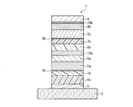
- FIG. 1 is a cross-sectional view showing a configuration of an organic EL element according to the first embodiment of the present invention.
- the organic EL element 1 of the present embodiment includes a substrate 2, an anode 3 provided on the substrate 2, and a cathode 4 provided above the anode 3.
- a light emitting layer 5 as a recombination layer is provided between the anode 3 and the cathode 4.
- a buffer layer 6, a hole transport layer 7, and a hole injection layer 8 are sequentially provided between the anode 3 and the light emitting layer 5 from the light emitting layer 5 toward the anode 3. Yes.
- an electron transport layer 9 and an electron injection layer 10 are sequentially provided between the cathode 4 and the light emitting layer 5 from the light emitting layer 5 toward the cathode 4.
- the substrate 2 is made of a material such as glass.
- a transparent electrode material such as ITO is used.
- the thickness of the anode 3 is, for example, about 20 nm to 100 nm.
- the cathode 4 aluminum or silver is used for the cathode 4.
- the thickness of the cathode 4 is flexible, but for example, in the case of a top emission structure in which light is extracted to the cathode 4 side, it is generally preferable that the thickness is about several nm to 30 nm. In the case of a bottom emission structure in which light is extracted to the substrate 2 side, it may be several tens of nm.
- a transparent electrode material such as ITO or IZO may be used.
- the light emitting layer 5 is a recombination layer (active layer) in which electrons and holes can be recombined, and includes at least a host and a light emitting dopant.
- the light emitting dopant material either a fluorescent dopant material or a phosphorescent dopant material can be used.
- fluorescent dopant materials include diamine pyrene-based blue delayed fluorescent materials.
- the phosphorescent dopant material include tris (2-phenylpyridinate) iridium (III) (Ir (ppy) 3).
- the (luminescent) host material examples include 1,3,5-tris (N-phenylbenzoimidazol-2-yl) benzene (TPBI).
- TPBI 1,3,5-tris (N-phenylbenzoimidazol-2-yl) benzene
- the thickness of the light emitting layer 5 is about 40 nm, for example.
- the buffer layer 6 is made of an alkali metal, alkaline earth metal, or organic material having an electron donating property. More specifically, the buffer layer 6 is made of an alkali metal such as lithium, sodium, or cesium, an alkaline earth metal such as magnesium, calcium, strontium, or barium, or an organic material such as BPhen (vasophenanthroline). . Further, the thickness of the buffer layer 6 is set to a value in the range of 0.1 nm to 1 nm, for example, and is 5% or less of the thickness of the light emitting layer (recombination layer) 5.
- the buffer layer 6 is configured to suppress the electron trapping property due to the contamination in the light emitting layer 5 due to the electron donating property (details will be described later).
- the hole transport layer 7 for example, a layer possessed by a normal organic EL element can be used.
- a layer possessed by a normal organic EL element can be used.
- the thickness of the hole transport layer 7 is, for example, 15 nm.
- Examples of the hole injection layer 8 include phthalocyanine materials, starburst polyamines, and polyanilines.
- the thickness of the hole injection layer 8 is, for example, several tens of nm.
- the electron transport layer 9 is, for example, 20 nm.
- the buffer layer 6 is made of BPhen made of the same material as that of the electron transport layer 9, an organic EL element having a simple structure and excellent light emission characteristics can be easily formed.
- the electron injection layer 10 for example, metal lithium, metal barium, or the like, or a compound such as lithium fluoride, which is a compound thereof, is used.
- the thickness of the electron injection layer 10 is often very thin, for example, 0.1 nm.
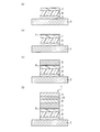
- FIG. 2A to FIG. 2D are diagrams for explaining the manufacturing process of the organic EL element.
- the anode 3, the hole injection layer 8, and the hole transport layer 7 are sequentially formed on the substrate 2 by using, for example, a vacuum deposition method. .
- the anode 3, the hole injection layer 8, and the hole transport layer 7 are sequentially transferred into separate vapor deposition chambers provided in a vapor deposition apparatus (not shown), and sequentially formed in the corresponding vapor deposition chambers. It has come to be.
- the buffer layer 6 is formed on the hole transport layer 7 by using, for example, a vacuum deposition method.
- the buffer layer 6 is formed in a dedicated vapor deposition chamber provided in the vapor deposition apparatus.
- a dedicated deposition source is installed in the deposition chamber for the hole transport layer 7
- a dedicated deposition source is installed in the deposition chamber for the light emitting layer 5
- the buffer layer 6 is formed. It may be configured to form a film.
- the light emitting layer 5 is formed on the buffer layer 6 by using, for example, a vacuum deposition method.
- the light emitting layer 5 is formed in a dedicated vapor deposition chamber provided in the vapor deposition apparatus.
- the electron transport layer 9, the electron injection layer 10, and the cathode 4 are sequentially formed on the light emitting layer 5 by using, for example, a vacuum deposition method.
- the electron transport layer 9, the electron injection layer 10, and the cathode 4 are sequentially transferred into separate vapor deposition chambers provided in a vapor deposition apparatus (not shown), and are sequentially formed in the corresponding vapor deposition chambers. It is like that.
- the organic EL element 1 of the present embodiment is manufactured.
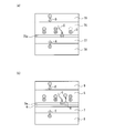
- FIG. 3A is a diagram for explaining the operation in the comparative example
- FIG. 3B is a diagram for explaining the operation in the product of the present embodiment.
- the comparative example is an equivalent of a conventional organic EL element, and includes a stacked hole injection layer 78, hole transport layer 77, light emitting layer 75, and electron transport layer 79. Further, in this comparative example, a contamination existing region 75 a is generated in the light emitting layer 75 in the vicinity of the interface with the hole transport layer 77.
- a hole transport layer is formed from the hole injection layer 78 so that holes injected from an anode (not shown) are directed into the light emitting layer 75. 77 flows in.
- electrons injected from a cathode (not shown) flow in the electron transport layer 79 so as to go into the light emitting layer 75.
- most of the electrons and holes are recombined to generate a light emission phenomenon.
- the organic EL element when the recombination of electrons and holes is inhibited in the light emitting layer 75, the organic EL element has a decrease in light emission characteristics such as a decrease in luminance and light emission unevenness and a decrease in lifetime. It will occur.
- holes injected from an anode are directed from the hole injection layer 8 so as to go into the light emitting layer 5. It flows in the hole transport layer 7.
- electrons injected from a cathode flow in the electron transport layer 9 so as to go into the light emitting layer 5.
- all electrons and holes can be recombined, and an appropriate light emission phenomenon occurs.
- the buffer layer 6 even if the contamination existing region 5a is generated in the light emitting layer 5 in the vicinity of the interface with the hole transport layer 7, the buffer layer 6 generates holes that cannot be recombined. Can be prevented. Specifically, as shown by arrow G in FIG. 3B, even if electrons are trapped by contamination, the electrons are buffered as shown by arrow H in FIG. It can be re-donated by the layer 6 into the light-emitting layer 5 to recombine with holes.
- the organic EL element 1 of the present embodiment configured as described above, even when contamination exists in the light emitting layer (active layer) 5, the electron trapping property caused by the contamination is caused by the buffer layer 6. Can be suppressed. Thereby, in this embodiment, unlike the said prior art example, it can prevent that the function of the light emitting layer 5 falls, and can comprise the organic EL element 1 provided with the outstanding light emission characteristic.
- the buffer layer 6 is composed of an alkali metal, an alkaline earth metal, or an organic substance having an electron donating property, so that the electron trapping property can be reliably suppressed.
- the thickness of the buffer layer 6 is a value within the range of 0.1 nm to 1 nm, the buffer layer 6 can be prevented from affecting the characteristics of the organic EL element 1, The deterioration of the characteristics can be prevented.
- the thickness of the buffer layer 6 is 5% or less of the thickness of the light emitting layer 5, it is ensured that the buffer layer 6 affects the characteristics of the organic EL element 1. It can prevent, and it can prevent reliably that the characteristic falls.
- FIG. 4 is a cross-sectional view showing a configuration of an organic EL element according to the second embodiment of the present invention.
- the main difference between this embodiment and the first embodiment is that a red light emitting layer that emits red light, a green light emitting layer that emits green light, and blue light.
- the blue light emitting layer is provided.
- symbol is attached
- the red sub-pixel PR that emits red (R) light, and the green sub-pixel PR that emits green (G) light on the substrate 2, the red sub-pixel PR that emits red (R) light, and the green sub-pixel PR that emits green (G) light.
- a sub pixel PG and a blue sub pixel PB that emits blue (B) light are provided, and one pixel is configured by the RGB sub pixels PR, PG, and PB.
- TFT 41 switching element
- wiring 43 interlayer film 42 (interlayer insulating film, planarization film), edge cover 44, and the like are provided.
- the TFT 41 functions as a switching element that controls each light emission of the sub-pixels PR, PG, and PB, and is provided for each of the sub-pixels PR, PG, and PB.
- the TFT 41 is connected to the wiring 43.
- the interlayer film 42 also functions as a planarizing film, and is laminated on the entire display area on the substrate 2 so as to cover the TFT 41 and the wiring 43.
- the anode 13 is formed for each of the sub-pixels PR, PG, and PB. That is, the sub pixel PR is provided with a red anode 13R, the sub pixel PG is provided with a green anode 13G, and the sub pixel PB is provided with a blue anode 13B.
- the anodes 13R, 13G, and 13B are electrically connected to the TFT 41 through contact holes 42a formed in the interlayer film 42.
- the edge cover 44 is formed on the interlayer film 42 so as to cover the pattern end of the anode 13.
- the edge cover 44 is configured such that the organic EL layer between the anode 13 and the cathode 14 becomes thin at the pattern end portion of the anode 13 or electric field concentration occurs, so that the anode 13 and the cathode 14 constituting the organic EL element 1 Is an insulating layer for preventing short circuit.
- the edge cover 44 is provided with openings 44R, 44G, and 44B for each of the sub-pixels PR, PG, and PB.
- the openings 44R, 44G, and 44B of the edge cover 44 serve as light emission regions of the sub-pixels PR, PG, and PB.
- the sub-pixels PR, PG, and PB are partitioned by the edge cover 44 having an insulating property.
- the edge cover 44 also functions as an element isolation film.
- the organic EL element 1 of the present embodiment is a light emitting element capable of high luminance emission by low voltage direct current drive, and includes an anode 13, a cathode 14, and an organic EL layer between the anode 13 and the cathode 14. ing.
- the organic EL element 1 of the present embodiment As the organic EL layer, from the anode 13 side, the hole injection / hole transport layer 17 ′, the buffer layer 16, the light emitting layers 15R, 15G, and 15B, and the electron transport layer 19 are used. , And the electron injection layer 20 in this order.
- the hole injection layer / hole transport layer 17 ′ has both a function as a hole injection layer and a function as a hole transport layer, and is formed in common for the subpixels PR, PG, and PB. Has been. Similarly, the buffer layer 16, the electron transport layer 19, the electron injection layer 20, and the cathode 14 are formed in common for the subpixels PR, PG, and PB.
- the red light emitting layer 15R that emits red light
- the green light emitting layer 15G that emits green light
- a blue light emitting layer 15B that emits light is provided. That is, in the organic EL element 1 of the present embodiment, RGB coating layers are formed.
- a hole injection layer, a hole transport layer, an electron transport layer, an electron injection layer, and a cathode may be provided for each color of RGB.
- a configuration in which a TFT 41 or the like is provided may be used as in the present embodiment.
- the present embodiment can achieve the same operations and effects as the first embodiment.
- a red light emitting layer 15R that emits red light a green light emitting layer 15G that emits green light, and a blue light emitting layer 15B that emits blue light are provided.
- An anode 13R for green, an anode 13G for green, and an anode 13B for blue are provided.
- the organic EL element 1 which has the outstanding luminescent property which can perform color light emission can be comprised, without providing a color filter.
- the organic EL element 1 having excellent light emission characteristics that are easy to manufacture and capable of color light emission can be configured.
- FIG. 5 is a cross-sectional view showing a configuration of an organic EL element according to the third embodiment of the present invention.
- the main difference between this embodiment and the first embodiment is that an electron injection layer, an electron transport layer, a light emitting layer, a buffer layer, a hole transport layer, and a positive electrode are provided between the anode and the cathode.
- an electron injection layer, an electron transport layer, a light emitting layer, a buffer layer, a hole transport layer, and a positive electrode are provided between the anode and the cathode.
- a plurality of sets of hole injection layers are provided.
- symbol is attached
- the first hole injection layer 8 a and the first hole transport layer 7 a are sequentially formed on the anode 3 provided on the substrate 2.
- a first buffer layer 6a, a first light emitting layer 5a, a first electron transport layer 9a, and a first electron injection layer 10a are sequentially formed on the first hole transport layer 7a.
- the second hole injection layer 8b and the second hole transport layer 7b are sequentially formed on the first electron injection layer 10a.
- a second buffer layer 6b, a second light emitting layer 5b, a second electron transport layer 9b, and a second electron injection layer 10b are sequentially formed on the second hole transport layer 7b.
- a cathode 4 is provided on 10b. That is, in the organic EL element 1 of the present embodiment, two sets of the electron injection layer, the electron transport layer, the light emitting layer, the buffer layer, the hole transport layer, and the hole injection layer are provided between the anode 3 and the cathode 4. A tandem structure is provided.
- the present embodiment can achieve the same operations and effects as the first embodiment.
- the organic EL element 1 having a tandem structure is configured, the high-quality organic EL element 1 with reduced power consumption can be easily configured.
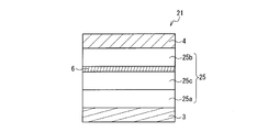
- FIG. 6 is sectional drawing which shows the structure of the organic thin film solar cell concerning the 4th Embodiment of this invention.
- the main difference between the present embodiment and the first embodiment is that an organic thin-film solar cell having a power generation layer as an active layer is configured.
- an organic thin-film solar cell having a power generation layer as an active layer is configured.
- symbol is attached
- the organic thin film solar cell 21 of the present embodiment includes a power generation layer 25 as a recombination layer between the anode 3 and the cathode 4.
- the power generation layer 25 includes a p-type organic semiconductor 25a, an i-type organic semiconductor 25c, and an n-type organic semiconductor 25b.
- the p-type organic semiconductor 25a is connected to the anode 3 as a p-type electrode.
- the n-type organic semiconductor 25b is connected to the cathode 4 as an n-type electrode.
- the buffer layer 6 exists between the i-type organic semiconductor 25c and the n-type organic semiconductor 25b.
- the buffer layer 6 is made of an alkali metal, an alkaline earth metal, or an organic material having an electron donating property, as in the first embodiment. In the buffer layer 6, even if contamination exists in the i-type organic semiconductor 25c, and electrons generated in the power generation layer 25 are trapped (captured) by the contamination, the electron donating property Thus, electrons can flow to the cathode 4.
- the power generation function of the power generation layer 25 can be prevented from being lowered, and the organic thin film solar cell 21 having excellent power generation performance can be configured.
- FIG. 7 is sectional drawing which shows the structure of the organic thin-film diode concerning the 5th Embodiment of this invention.
- the main difference between the present embodiment and the first embodiment is that an organic thin film diode that does not emit light is configured.
- symbol is attached
- the organic thin film diode 31 of this embodiment includes a recombination layer 32 between the anode 3 and the cathode 4.
- the recombination layer 32 includes a p-type organic semiconductor 32a, an i-type organic semiconductor 32c, and an n-type organic semiconductor 32b.
- the p-type organic semiconductor 32a is connected to the anode 3 as a p-type electrode.
- the n-type organic semiconductor 32b is connected to the cathode 4 as an n-type electrode.
- the buffer layer 6 exists between the i-type organic semiconductor 32c and the p-type organic semiconductor 32a.
- the buffer layer 6 is made of an alkali metal, an alkaline earth metal, or an organic material having an electron donating property, as in the first embodiment. In the buffer layer 6, even if contamination exists in the p-type organic semiconductor 32 a and electrons flowing in the recombination layer 32 are trapped (captured) by the contamination, Due to the donating property, electrons can be donated and recombined with holes.
- the present embodiment it is possible to prevent the recombination function of the recombination layer 32 from being lowered, and it is possible to configure the organic thin film diode 31 having excellent diode performance.
- the present invention suppresses the electron trapping property on the anode side or the cathode side of the recombination layer in the organic element having the anode, the cathode, and the recombination layer provided between the anode and the cathode.
- a buffer layer is provided.
- the buffer layer configured to have a uniform thickness has been described, but the buffer layer of the present invention is not limited to this. That is, since the buffer layer is formed extremely thin using a vacuum deposition method, it may be configured in an island shape with a non-uniform film thickness.
- the configuration in which the light emitting layer, the hole transport layer, and the electron transport layer are separately provided has been described.
- the organic EL element of the present invention is not limited to this.
- a configuration in which a light emitting layer that also serves as a hole transport layer is used, or a light emitting layer that also serves as an electron transport layer may be used.
- the present invention is useful for an organic element having excellent characteristics capable of preventing the function of the recombination layer from being deteriorated.
- Organic EL device organic device 3, 13R, 13G, 13B Anode 4, 14 Cathode 5, 15R, 15G, 15B, 5a, 5b
- Light emitting layer (recombination layer) 6, 16, 6a, 6b Buffer layer 7, 17 ′, 7a, 7b Hole transport layer 8, 17 ′, 8a, 8b Hole injection layer 9, 19, 9a, 9b
- Electron transport layer 10 20, 10a, 10b Electron injection layer 21
- Organic thin-film solar cell 25
- Power generation layer (recombination layer) 31
- Organic thin-film diode 32 Recombination layer
Abstract
陽極(3)と、陰極(4)と、これらの陽極(3)と陰極(4)との間に設けられた発光層(再結合層)(5)を有する有機EL素子(1)において、発光層(5)と陰極(4)との間には、発光層(5)から陰極(4)側に向かって電子輸送層(9)及び電子注入層(10)を順次設けた。また、発光層(5)と陽極(3)との間には、陽極(3)から発光層(5)側に向かって正孔注入層(8)及び正孔輸送層(7)を順次設けた。さらに、発光層(5)と正孔輸送層(7)との間には、電子トラップ性を抑制するバッファ層(6)を設けた。
Description
本発明は、有機EL表示装置や有機EL照明装置に用いられる有機EL(エレクトロルミネッセンス)素子、あるいは有機薄膜太陽電池などの有機化合物を用いた活性層を有する有機素子に関する。
近年、OLED(有機ELディスプレイ)に代表される有機素子は、陽極、陰極、及び有機化合物によって構成されるとともに、陽極と陰極の間に設けられて、電子とホール(正孔)とが再結合可能な再結合層(活性層)を備えている。また、このような有機素子では、その機能や動作効率などを向上させるために、陽極と再結合層との間、及び/または陰極と再結合層との間に、様々な層を設けることが行われている。
具体的にいえば、従来の有機EL素子では、例えば下記特許文献1に記載されているように、陽極と再結合層としての発光層との間において、陽極から発光層側に向かって、正孔注入層及び正孔輸送層を順次設けることが提案されている。また、この従来の有機EL素子では、陰極と発光層との間において、陰極から発光層側に向かって、電子注入層及び電子輸送層を順次設けることが提案されている。そして、この従来の有機EL素子では、発光層での正孔と電子との再結合を効率よく行わせて、当該発光層での発光効率を向上させ、ひいては有機EL素子の発光特性をも向上させることが可能とされていた。
しかしながら、上記のような従来の有機EL素子(有機素子)では、発光層(再結合層)の機能が低下し、ひいては有機EL素子の発光特性も低下するという問題点を発生することがあった。
具体的にいえば、従来の有機EL素子では、例えばスピンコート法を用いて、陽極上に正孔注入層を形成した後、真空蒸着法を用いて、正孔注入層上に正孔輸送層、発光層、電子輸送層、電子注入層、及び陰極を順次形成していた。このように、従来の有機EL素子では、複数の蒸着チャンバー内を順次搬送しながら、正孔輸送層、発光層、電子輸送層、電子注入層、及び陰極を順次設けていた。このため、従来の有機EL素子では、発光層内にコンタミネーションが存在することがあった。
例えば、詳細に記載すると、複数の各蒸着チャンバーでは、その可動部分にグリスが塗布されており、このグリスの成分がコンタミネーションとして発光層内に混入することがあった。また、複数の各蒸着チャンバーでは、その蒸着源の近傍が高温となるため、有機EL素子の構成材料が長時間の間、熱にさらされることによって変質し、その変質成分がコンタミネーションとして発光層内に混入することがあった。
そして、従来の有機EL素子では、コンタミネーションの濃度や成分などによっては、発光層、特に発光層の陽極側の界面、つまり発光層と正孔輸送層との界面近傍において、電子がコンタミネーションによってトラップ(捕獲)されることがあった。この結果、従来の有機EL素子では、発光層での正孔と電子との再結合の効率の低下を発生して、有機EL素子の発光輝度の低下や発光ムラの発生などが生じて、発光特性が低下するという問題点を生じることがあった。
上記の課題を鑑み、本発明は、再結合層の機能が低下するのを防ぐことができる優れた特性を備えた有機素子を提供することを目的とする。
上記の目的を達成するために、本発明にかかる有機素子は、陽極と、陰極と、これらの陽極と陰極との間に設けられた再結合層を有する有機素子であって、
前記活性層の前記陽極側または前記陰極側に、電子トラップ性を抑制するバッファ層を設けたことを特徴とするものである。
前記活性層の前記陽極側または前記陰極側に、電子トラップ性を抑制するバッファ層を設けたことを特徴とするものである。
上記のように構成された有機素子では、再結合層内にコンタミネーションが存在している場合でも、バッファ層により、コンタミネーションに起因する、電子トラップ性を抑制することができる。これにより、上記従来例と異なり、再結合層の機能が低下するのを防ぐことができ、優れた特性を備えた有機素子を構成することができる。
また、上記有機素子において、前記バッファ層は、電子供与性を有する、アルカリ金属、アルカリ土類金属、または有機物により、構成されていることが好ましい。
この場合、上記電子トラップ性を確実に抑制することができる。
また、上記有機素子において、前記バッファ層の厚さが、0.1nm~1nmの範囲内の値であることが好ましい。
この場合、バッファ層が有機素子の特性に影響を与えることを防ぐことができ、特性が低下するのを防止することができる。
また、上記有機素子において、前記バッファ層の厚さは、前記再結合層の厚さの5%以下の厚さであることが好ましい。
この場合、バッファ層が有機素子の特性に影響を与えることを確実に防ぐことができ、特性が低下するのを確実に防止することができる。
また、上記有機素子において、前記再結合層として、発光層が設けられ、
前記発光層と前記陰極との間には、前記発光層から前記陰極側に向かって電子輸送層及び電子注入層が順次設けられ、
前記発光層と前記陽極との間には、前記発光層から前記陽極側に向かって前記バッファ層、正孔輸送層、及び正孔注入層が順次設けられてもよい。
前記発光層と前記陰極との間には、前記発光層から前記陰極側に向かって電子輸送層及び電子注入層が順次設けられ、
前記発光層と前記陽極との間には、前記発光層から前記陽極側に向かって前記バッファ層、正孔輸送層、及び正孔注入層が順次設けられてもよい。
この場合、発光層の機能が低下するのを防ぐことができる優れた発光特性を備えた有機EL素子を構成することができる。
また、上記有機素子において、前記発光層として、赤色の光を発光する赤色の発光層と、緑色の光を発光する緑色の発光層と、青色の光を発光する青色の発光層とが設けられ、
前記陽極には、前記赤色の発光層に対応して設けられた赤色用の陽極と、前記緑色の発光層に対応して設けられた緑色用の陽極と、前記青色の発光層に対応して設けられた青色用の陽極とが含まれてもよい。
前記陽極には、前記赤色の発光層に対応して設けられた赤色用の陽極と、前記緑色の発光層に対応して設けられた緑色用の陽極と、前記青色の発光層に対応して設けられた青色用の陽極とが含まれてもよい。
この場合、カラーフィルターを設けることなく、カラー発光が可能な優れた発光特性を有する有機EL素子を構成することができる。
また、上記有機素子において、前記陰極、前記電子注入層、前記電子輸送層、前記バッファ層、前記正孔輸送層、及び前記正孔注入層のうち、少なくとも前記バッファ層が、前記赤色の発光層、前記緑色の発光層、及び前記青色の発光層に共通して設けられてもよい。
この場合、製造簡単で、カラー発光が可能な優れた発光特性を有する有機EL素子を構成することができる。
また、上記有機素子において、前記陽極と前記陰極との間に、前記電子注入層、前記電子輸送層、前記発光層、前記バッファ層、前記正孔輸送層、及び前記正孔注入層の組が複数組設けられてもよい。
この場合、タンデム構造の有機EL素子を構成することができ、消費電力を抑えた高品位な有機EL素子を容易に構成することができる。
また、上記有機素子において、前記バッファ層と前記電子輸送層とが、同じ材料を用いて構成されていることが好ましい。
この場合、構造簡単で、優れた発光特性を有する有機EL素子を容易に構成することができる。
また、上記有機素子において、前記再結合層として、前記陽極側に設けられたp型の有機半導体と、前記陰極側に設けられたn型の有機半導体と、前記p型の有機半導体と前記n型の有機半導体との間に設けられたi型の有機半導体とを有する発電層が設けられ、
前記i型の有機半導体と前記n型の有機半導体との間には、前記バッファ層が設けられてもよい。
前記i型の有機半導体と前記n型の有機半導体との間には、前記バッファ層が設けられてもよい。
この場合、発電層の機能が低下するのを防ぐことができる優れた発電特性を備えた有機薄膜太陽電池を構成することができる。
また、上記有機素子において、前記再結合層として、前記陽極側に設けられたp型の有機半導体と、前記陰極側に設けられたn型の有機半導体と、前記p型の有機半導体と前記n型の有機半導体との間に設けられたi型の有機半導体とが設けられ、
前記i型の有機半導体と前記p型の有機半導体との間には、前記バッファ層が設けられてもよい。
前記i型の有機半導体と前記p型の有機半導体との間には、前記バッファ層が設けられてもよい。
この場合、再結合層の機能が低下するのを防ぐことができる優れた特性を備えた有機薄膜ダイオードを構成することができる。
本発明によれば、再結合層の機能が低下するのを防ぐことができる優れた特性を備えた有機素子を提供することが可能となる。
以下、本発明の有機素子の好ましい実施形態について、図面を参照しながら説明する。なお、以下の説明では、本発明を有機EL素子、有機薄膜太陽電池、または有機薄膜ダイオードに適用した場合を例示して説明する。また、各図中の構成部材の寸法は、実際の構成部材の寸法及び各構成部材の寸法比率等を忠実に表したものではない。
[第1の実施形態]
図1は、本発明の第1の実施形態にかかる有機EL素子の構成を示す断面図である。図1において、本実施形態の有機EL素子1は、基板2と、基板2上に設けられた陽極3と、陽極3の上方に設けられた陰極4を備えている。また、有機EL素子1では、陽極3と陰極4との間に、再結合層としての発光層5が設けられている。また、有機EL素子1では、陽極3と発光層5との間に、発光層5から陽極3側に向かってバッファ層6、正孔輸送層7、及び正孔注入層8が順次設けられている。さらに、有機EL素子1では、陰極4と発光層5との間に、発光層5から陰極4側に向かって電子輸送層9及び電子注入層10が順次設けられている。
図1は、本発明の第1の実施形態にかかる有機EL素子の構成を示す断面図である。図1において、本実施形態の有機EL素子1は、基板2と、基板2上に設けられた陽極3と、陽極3の上方に設けられた陰極4を備えている。また、有機EL素子1では、陽極3と陰極4との間に、再結合層としての発光層5が設けられている。また、有機EL素子1では、陽極3と発光層5との間に、発光層5から陽極3側に向かってバッファ層6、正孔輸送層7、及び正孔注入層8が順次設けられている。さらに、有機EL素子1では、陰極4と発光層5との間に、発光層5から陰極4側に向かって電子輸送層9及び電子注入層10が順次設けられている。
基板2には、例えばガラスなどの材料が用いられている。陽極3には、例えばITOなどの透明電極材料が用いられている。また、この陽極3の厚さは、例えば20nm~100nm程度である。
陰極4には、例えばアルミニウム、銀などが使われている。また、陰極4の厚みは自由度があるが、例えば陰極4側に光を取り出すトップエミッション構造の場合は、一般的に数nm~30nm程度である場合が好ましい。また、基板2側に光を取り出すボトムエミッション構造の場合は、数10nmで構わない。また、ITOやIZOなどの透明電極材料を用いてもよい。
発光層5は、電子と正孔とが再結合可能な再結合層(活性層)であり、少なくともホストと発光ドーパントを含んでいる。また、この発光層5では、例えば発光ドーパント材料としては、蛍光ドーパント材料又は燐光ドーパント材料のどちらでも用いることができる。また、蛍光ドーパント材料としては、例えば、ジアミンピレン系の青色遅延蛍光材料等が挙げられる。また、燐光ドーパント材料としては、例えば、トリス(2-フェニルピリジナート)イリジウム(III)(Ir(ppy)3)等が挙げられる。また、(発光)ホスト材料としては、例えば、1,3,5-トリス(N-フェニルベンゾイミダゾール-2-イル)ベンゼン(TPBI)等が挙げられる。また、発光層5の厚さは、例えば40nm程度である。
バッファ層6には、電子供与性を有する、アルカリ金属、アルカリ土類金属、または有機物が用いられている。具体的にいえば、バッファ層6には、リチウム、ナトリウム、セシウムなどのアルカリ金属、マグネシウム、カルシウム、ストロンチウム、バリウムなどのアルカリ土類金属、またはBPhen(バソフェナントロリン)などの有機物が使用されている。また、このバッファ層6の厚さは、例えば0.1nm~1nmの範囲内の値に設定されており、発光層(再結合層)5の厚さの5%以下の値とされている。
そして、このバッファ層6は、その電子供与性により、発光層5内のコンタミネーションに起因する電子トラップ性を抑制するように構成されている(詳細は後述。)。
正孔輸送層7には、例えば通常の有機EL素子が有するものを用いることができ、例えば、4,4’-ビス[N-(1-ナフチル)-N-フェニル-アミノ]-ビフェニル(α-NPD)等が挙げられる。また、この正孔輸送層7の厚さは、例えば15nmである。
正孔注入層8には、例えばフタロシアニン系材料や、スターバーストポリアミン類や、ポリアニリン類などが挙げられる。この正孔注入層8の厚さは、例えば数10nmである。
電子輸送層9には、例えばBPhenが用いられている。また、この電子輸送層9の厚さは、例えば20nmである。
なお、上記バッファ層6を電子輸送層9と同じ材料のBPhenにて構成した場合、構造簡単で、優れた発光特性を有する有機EL素子を容易に構成することができる。
電子注入層10には、例えば金属リチウムや、金属バリウムなど、もしくはそれらの化合物であるリチウムフロライドのような物が用いられている。また、この電子注入層10の厚さは、非常に薄い場合が多く、例えば0.1nmである。
次に、図2(a)~図2(d)を用いて、本実施形態の有機EL素子1の製造方法について具体的に説明する。
図2(a)~図2(d)は、上記有機EL素子の製造工程を説明する図である。
図2(a)において、本実施形態の有機EL素子1では、陽極3、正孔注入層8、及び正孔輸送層7が、例えば真空蒸着法を用いて、基板2上に順次形成される。これらの陽極3、正孔注入層8、及び正孔輸送層7は、蒸着装置(図示しない)に設けられた別個の蒸着チャンバー内に順番に搬送されて、対応する蒸着チャンバー内で順次成膜されるようになっている。
次に、図2(b)に示すように、バッファ層6が、例えば真空蒸着法を用いて、正孔輸送層7上に形成される。このバッファ層6は、上記蒸着装置に設けられた専用の蒸着チャンバー内で成膜される。なお、この説明以外に、正孔輸送層7用の蒸着チャンバー内に専用の蒸着源を設置したり、発光層5用の蒸着チャンバー内に専用の蒸着源を設置したり、バッファ層6を成膜する構成でもよい。
続いて、図2(c)に示すように、発光層5が、例えば真空蒸着法を用いて、バッファ層6上に形成される。この発光層5は、上記蒸着装置に設けられた専用の蒸着チャンバー内で成膜される。
次に、図2(d)に示すように、電子輸送層9、電子注入層10、及び陰極4が、例えば真空蒸着法を用いて、発光層5上に順次形成される。これらの電子輸送層9、電子注入層10、及び陰極4は、蒸着装置(図示しない)に設けられた別個の蒸着チャンバー内に順番に搬送されて、対応する蒸着チャンバー内で順次成膜されるようになっている。
以上の製造工程により、本実施形態の有機EL素子1は、製造される。
次に、図3(a)及び図3(b)を参照して、バッファ層6の機能について具体的に説明する。
図3(a)は、比較例での動作を説明する図であり、図3(b)は、本実施形態品での動作を説明する図である。
図3(a)において、比較例は、従来の有機EL素子の相当品であり、積層された正孔注入層78、正孔輸送層77、発光層75、及び電子輸送層79を備えている。また、この比較例では、コンタミネーションの存在領域75aが発光層75内で正孔輸送層77との界面近傍に生じている。
また、この比較例では、図3(a)に矢印Aにて示すように、図示しない陽極から注入された正孔が発光層75内に向かうように正孔注入層78内から正孔輸送層77内に流れる。また、この比較例では、図3(a)に矢印Bにて示すように、図示しない陰極から注入された電子が発光層75内に向かうように電子輸送層79内を流れる。そして、この比較例の発光層75内では、大部分の電子と正孔が再結合して、発光現象が生じる。
しかしながら、この比較例では、上記コンタミネーションの存在領域75aにおいて、そのコンタミネーションの濃度や成分などによっては、図3(a)に矢印Cにて示すように、電子は当該コンタミネーションにトラップ(捕獲)されてしまう。この結果、この比較例では、図3(a)にDにて示すように、再結合できなかった正孔が生じる。
また、この比較例のように、発光層75において、電子と正孔の再結合が阻害されると、輝度の低下や発光ムラなどの発光特性の低下や、寿命の低下などが有機EL素子に生じてしまう。
これに対して、本実施形態品では、図3(b)に矢印Eにて示すように、図示しない陽極から注入された正孔が発光層5内に向かうように正孔注入層8内から正孔輸送層7内に流れる。また、この本実施形態品では、図3(b)に矢印Fにて示すように、図示しない陰極から注入された電子が発光層5内に向かうように電子輸送層9内を流れる。そして、この本実施形態品の発光層5内では、比較例と異なり、全ての電子と正孔との再結合が可能となり、適切な発光現象が生じる。
すなわち、この本実施形態品では、たとえコンタミネーションの存在領域5aが発光層5内で正孔輸送層7との界面近傍に生じていたとしても、バッファ層6により、再結合できない正孔の発生を防ぐことができる。具体的にいえば、図3(b)に矢印Gにて示すように、たとえ電子がコンタミネーションによってトラップされてしまっても、図3(b)に矢印Hにて示すように、電子はバッファ層6によって発光層5内に再供与されて、正孔と再結合することができる。
以上のように構成された本実施形態の有機EL素子1では、発光層(活性層)5内にコンタミネーションが存在している場合でも、バッファ層6により、コンタミネーションに起因する、電子トラップ性を抑制することができる。これにより、本実施形態では、上記従来例と異なり、発光層5の機能が低下するのを防ぐことができ、優れた発光特性を備えた有機EL素子1を構成することができる。
また、本実施形態では、バッファ層6は、電子供与性を有する、アルカリ金属、アルカリ土類金属、または有機物により、構成されているので、上記電子トラップ性を確実に抑制することができる。
また、本実施形態では、バッファ層6の厚さが0.1nm~1nmの範囲内の値であるので、当該バッファ層6が有機EL素子1の特性に影響を与えることを防ぐことができ、その特性が低下するのを防止することができる。
また、本実施形態では、バッファ層6の厚さは発光層5の厚さの5%以下の厚さであるので、当該バッファ層6が有機EL素子1の特性に影響を与えることを確実に防ぐことができ、その特性が低下するのを確実に防止することができる。
[第2の実施形態]
図4は、本発明の第2の実施形態にかかる有機EL素子の構成を示す断面図である。
図4は、本発明の第2の実施形態にかかる有機EL素子の構成を示す断面図である。
図において、本実施形態と上記第1の実施形態との主な相違点は、赤色の光を発光する赤色の発光層と、緑色の光を発光する緑色の発光層と、青色の光を発光する青色の発光層を設けた点である。なお、上記第1の実施形態と共通する要素については、同じ符号を付して、その重複した説明を省略する。
つまり、図4に示すように、本実施形態の有機EL素子1では、基板2上において、赤色(R)の光を発射する赤色のサブ画素PR、緑色(G)の光を発射する緑色のサブ画素PG、及び青色(B)の光を発射する青色のサブ画素PBが設けられており、これらRGBのサブ画素PR、PG、及びPBによって1つの画素が構成されている。
また、基板2上には、TFT41(スイッチング素子)、配線43、層間膜42(層間絶縁膜、平坦化膜)、エッジカバー44等が設けられている。
TFT41はサブ画素PR、PG、及びPBの各発光を制御するスイッチング素子として機能するものであり、サブ画素PR、PG、及びPBごとに設けられる。TFT41は配線43に接続される。
層間膜42は、平坦化膜としても機能するものであり、TFT41及び配線43を覆うように基板2上の表示領域の全面に積層されている。
層間膜42上には、陽極13がサブ画素PR、PG、及びPBごとに形成されている。すなわち、サブ画素PRでは、赤色用の陽極13Rが設けられ、サブ画素PGでは、緑色用の陽極13Gが設けられ、サブ画素PBでは、青色用の陽極13Bが設けられている。各陽極13R、13G、及び13Bは、層間膜42に形成されたコンタクトホール42aを介して、TFT41に電気的に接続されている。
エッジカバー44は、層間膜42上に、陽極13のパターン端部を被覆するように形成されている。エッジカバー44は、陽極13のパターン端部で陽極13と陰極14との間の有機EL層が薄くなったり電界集中が起こったりすることで、有機EL素子1を構成する陽極13と陰極14とが短絡することを防止するための絶縁層である。
エッジカバー44には、サブ画素PR、PG、及びPB毎に開口44R、44G、及び44Bが設けられている。このエッジカバー44の開口44R、44G、及び44Bが、各サブ画素PR、PG、及びPBの発光領域となる。言い換えれば、各サブ画素PR、PG、及びPBは、絶縁性を有するエッジカバー44によって仕切られている。エッジカバー44は、素子分離膜としても機能する。
また、本実施形態の有機EL素子1は、低電圧直流駆動による高輝度発光が可能な発光素子であり、陽極13、陰極14、及びこれら陽極13と陰極14との間の有機EL層を備えている。
また、本実施形態の有機EL素子1では、上記有機EL層として、陽極13側から正孔注入層兼正孔輸送層17’、バッファ層16、発光層15R、15G、及び15B、電子輸送層19、及び電子注入層20をこの順に備えている。
正孔注入層兼正孔輸送層17’は、正孔注入層としての機能と正孔輸送層としての機能とを併せ持つものであり、サブ画素PR、PG、及びPBに対して、共通して形成されている。同様に、バッファ層16、電子輸送層19、電子注入層20、及び陰極14は、サブ画素PR、PG、及びPBに対して、共通して形成されている。
また、本実施形態の有機EL素子1では、共通のバッファ層16上に、赤色の光を発光する赤色の発光層15Rと、緑色の光を発光する緑色の発光層15Gと、青色の光を発光する青色の発光層15Bとが設けられている。すなわち、本実施形態の有機EL素子1では、RGBの塗分け層が形成されている。
尚、この説明以外に、例えば正孔注入層、正孔輸送層、電子輸送層、電子注入層、及び陰極の少なくとも1つをRGBの色毎に設ける構成でもよい。また、上記第1の実施形態の有機EL素子1及び後述の第3の実施形態の有機EL素子1においても、本実施形態と同様に、TFT41等を設ける構成でもよい。
以上の構成により、本実施形態では、上記第1の実施形態と同様な作用・効果を奏することができる。また、本実施形態では、赤色の光を発光する赤色の発光層15Rと、緑色の光を発光する緑色の発光層15Gと、青色の光を発光する青色の発光層15Bとが設けられ、赤色用の陽極13R、緑色用の陽極13G、及び青色用の陽極13Bとが設けられている。これにより、本実施形態では、カラーフィルターを設けることなく、カラー発光が可能な優れた発光特性を有する有機EL素子1を構成することができる。
また、本実施形態では、陰極、電子注入層、電子輸送層、バッファ層、正孔輸送層、及び正孔注入層のうち、少なくともバッファ層が、RGBの発光層15R、15G、15Bに共通して設けられているので、製造簡単で、カラー発光が可能な優れた発光特性を有する有機EL素子1を構成することができる。
[第3の実施形態]
図5は、本発明の第3の実施形態にかかる有機EL素子の構成を示す断面図である。
図5は、本発明の第3の実施形態にかかる有機EL素子の構成を示す断面図である。
図において、本実施形態と上記第1の実施形態との主な相違点は、陽極と陰極との間に、電子注入層、電子輸送層、発光層、バッファ層、正孔輸送層、及び正孔注入層の組を複数組設けた点である。なお、上記第1の実施形態と共通する要素については、同じ符号を付して、その重複した説明を省略する。
つまり、図5において、本実施形態の有機EL素子1では、基板2上に設けられた陽極3上に、第1正孔注入層8a及び第1正孔輸送層7aが順次形成されている。また、第1正孔輸送層7a上には、第1バッファ層6a、第1発光層5a、第1電子輸送層9a、及び第1電子注入層10aが順次形成されている。
さらに、本実施形態の有機EL素子1では、第1電子注入層10a上に、第2正孔注入層8b及び第2正孔輸送層7bが順次形成されている。また、第2正孔輸送層7b上には、第2バッファ層6b、第2発光層5b、第2電子輸送層9b、及び第2電子注入層10bが順次形成され、この第2電子注入層10b上には、陰極4が設けられている。すなわち、本実施形態の有機EL素子1では、陽極3と陰極4との間において、電子注入層、電子輸送層、発光層、バッファ層、正孔輸送層、及び正孔注入層の組を2組設けたタンデム構造とされている。
以上の構成により、本実施形態では、上記第1の実施形態と同様な作用・効果を奏することができる。また、本実施形態では、タンデム構造の有機EL素子1を構成しているので、消費電力を抑えた高品位な有機EL素子1を容易に構成することができる。
[第4の実施形態]
図6は、本発明の第4の実施形態にかかる有機薄膜太陽電池の構成を示す断面図である。
図6は、本発明の第4の実施形態にかかる有機薄膜太陽電池の構成を示す断面図である。
図において、本実施形態と上記第1の実施形態との主な相違点は、活性層として発電層を有する有機薄膜太陽電池を構成した点である。なお、上記第1の実施形態と共通する要素については、同じ符号を付して、その重複した説明を省略する。
つまり、図6において、本実施形態の有機薄膜太陽電池21は、陽極3と陰極4との間に、再結合層としての発電層25とを備えている。
発電層25は、p型の有機半導体25aと、i型の有機半導体25cと、n型の有機半導体25bを有している。p型の有機半導体25aは、p型電極としての陽極3に接続されている。また、n型の有機半導体25bは、n型電極としての陰極4に接続されている。バッファ層6が、i型の有機半導体25cとn型の有機半導体25bとの中間に存在している。
バッファ層6には、第1の実施形態のものと同様に、電子供与性を有する、アルカリ金属、アルカリ土類金属、または有機物が用いられている。そして、このバッファ層6では、たとえi型の有機半導体25c内にコンタミネーションが存在して、発電層25内で生じた電子が当該コンタミネーションによってトラップ(捕獲)されたとしても、その電子供与性により、電子を陰極4に流すことができる。
この結果、本実施形態では、発電層25の発電機能が低下するのを防ぐことができ、優れた発電性能を備えた有機薄膜太陽電池21を構成することができる。
[第5の実施形態]
図7は、本発明の第5の実施形態にかかる有機薄膜ダイオードの構成を示す断面図である。
図7は、本発明の第5の実施形態にかかる有機薄膜ダイオードの構成を示す断面図である。
図において、本実施形態と上記第1の実施形態との主な相違点は、発光を生じない有機薄膜ダイオードを構成した点である。なお、上記第1の実施形態と共通する要素については、同じ符号を付して、その重複した説明を省略する。
つまり、図7において、本実施形態の有機薄膜ダイオード31は、陽極3と陰極4との間に、再結合層32とを備えている。
再結合層32は、p型の有機半導体32aと、i型の有機半導体32cと、n型の有機半導体32bを有している。p型の有機半導体32aは、p型電極としての陽極3に接続されている。また、n型の有機半導体32bは、n型電極としての陰極4に接続されている。バッファ層6が、i型の有機半導体32cとp型の有機半導体32aとの中間に存在している。
バッファ層6には、第1の実施形態のものと同様に、電子供与性を有する、アルカリ金属、アルカリ土類金属、または有機物が用いられている。そして、このバッファ層6では、たとえp型の有機半導体32a内にコンタミネーションが存在して、再結合層32内に流れてきた電子が当該コンタミネーションによってトラップ(捕獲)されたとしても、その電子供与性により、電子を供与して、正孔と再結合させることができる。
この結果、本実施形態では、再結合層32の再結合機能が低下するのを防ぐことができ、優れたダイオード性能を備えた有機薄膜ダイオード31を構成することができる。
尚、上記の実施形態はすべて例示であって制限的なものではない。本発明の技術的範囲は特許請求の範囲によって規定され、そこに記載された構成と均等の範囲内のすべての変更も本発明の技術的範囲に含まれる。
例えば、上記の説明では、有機素子として有機EL素子、有機薄膜太陽電池、または有機薄膜ダイオードを用いた場合について説明した。しかしながら、本発明は、陽極と、陰極と、これらの陽極と陰極との間に設けられた再結合層を有する有機素子において、再結合層の陽極側または陰極側に、電子トラップ性を抑制するバッファ層を設けたものであれば何等限定されない。
また、上記の説明では、均一の厚さを有する層状に構成されたバッファ層について説明したが、本発明のバッファ層はこれに限定されない。すなわち、バッファ層は真空蒸着法を用いて極めて薄く形成されるので、膜厚が不均一な島状に構成されたものでもよい。
また、上記第1~第3の実施形態では、発光層、正孔輸送層、及び電子輸送層を別個に設けた構成について説明したが、本発明の有機EL素子はこれに限定されるものではなく、例えば正孔輸送層を兼用した発光層を用いたり、電子輸送層を兼用した発光層を用いたりする構成でもよい。
本発明は、再結合層の機能が低下するのを防ぐことができる優れた特性を備えた有機素子に対して有用である。
1 有機EL素子(有機素子)
3、13R、13G、13B 陽極
4、14 陰極
5、15R、15G、15B、5a、5b 発光層(再結合層)
6、16、6a、6b バッファ層
7、17'、7a、7b 正孔輸送層
8、17'、8a、8b 正孔注入層
9、19、9a、9b 電子輸送層
10、20、10a、10b 電子注入層
21 有機薄膜太陽電池
25 発電層(再結合層)
31 有機薄膜ダイオード
32 再結合層
3、13R、13G、13B 陽極
4、14 陰極
5、15R、15G、15B、5a、5b 発光層(再結合層)
6、16、6a、6b バッファ層
7、17'、7a、7b 正孔輸送層
8、17'、8a、8b 正孔注入層
9、19、9a、9b 電子輸送層
10、20、10a、10b 電子注入層
21 有機薄膜太陽電池
25 発電層(再結合層)
31 有機薄膜ダイオード
32 再結合層
Claims (11)
- 陽極と、陰極と、これらの陽極と陰極との間に設けられた再結合層を有する有機素子であって、
前記再結合層の前記陽極側または前記陰極側に、電子トラップ性を抑制するバッファ層を設けた、
ことを特徴とする有機素子。 - 前記バッファ層は、電子供与性を有する、アルカリ金属、アルカリ土類金属、または有機物により、構成されている請求項1に記載の有機素子。
- 前記バッファ層の厚さが、0.1nm~1nmの範囲内の値である請求項1または2に記載の有機素子。
- 前記バッファ層の厚さは、前記再結合層の厚さの5%以下の厚さである請求項3に記載の有機素子。
- 前記再結合層として、発光層が設けられ、
前記発光層と前記陰極との間には、前記発光層から前記陰極側に向かって電子輸送層及び電子注入層が順次設けられ、
前記発光層と前記陽極との間には、前記発光層から前記陽極側に向かって前記バッファ層、正孔輸送層、及び正孔注入層が順次設けられている請求項1~4のいずれか1項に記載の有機素子。 - 前記発光層として、赤色の光を発光する赤色の発光層と、緑色の光を発光する緑色の発光層と、青色の光を発光する青色の発光層とが設けられ、
前記陽極には、前記赤色の発光層に対応して設けられた赤色用の陽極と、前記緑色の発光層に対応して設けられた緑色用の陽極と、前記青色の発光層に対応して設けられた青色用の陽極とが含まれている請求項5に記載の有機素子。 - 前記陰極、前記電子注入層、前記電子輸送層、前記バッファ層、前記正孔輸送層、及び前記正孔注入層のうち、少なくとも前記バッファ層が、前記赤色の発光層、前記緑色の発光層、及び前記青色の発光層に共通して設けられている請求項6に記載の有機素子。
- 前記陽極と前記陰極との間に、前記電子注入層、前記電子輸送層、前記発光層、前記バッファ層、前記正孔輸送層、及び前記正孔注入層の組が複数組設けられている請求項5~7のいずれか1項に記載の有機素子。
- 前記バッファ層と前記電子輸送層とが、同じ材料を用いて構成されている請求項5~8のいずれか1項に記載の有機素子。
- 前記再結合層として、前記陽極側に設けられたp型の有機半導体と、前記陰極側に設けられたn型の有機半導体と、前記p型の有機半導体と前記n型の有機半導体との間に設けられたi型の有機半導体とを有する発電層が設けられ、
前記i型の有機半導体と前記n型の有機半導体との間には、前記バッファ層が設けられている請求項1~4のいずれか1項に記載の有機素子。 - 前記再結合層として、前記陽極側に設けられたp型の有機半導体と、前記陰極側に設けられたn型の有機半導体と、前記p型の有機半導体と前記n型の有機半導体との間に設けられたi型の有機半導体とが設けられ、
前記i型の有機半導体と前記p型の有機半導体との間には、前記バッファ層が設けられている請求項1~4のいずれか1項に記載の有機素子。
Priority Applications (1)
| Application Number | Priority Date | Filing Date | Title |
|---|---|---|---|
| US15/317,156 US10103202B2 (en) | 2014-06-12 | 2015-06-11 | Organic element |
Applications Claiming Priority (2)
| Application Number | Priority Date | Filing Date | Title |
|---|---|---|---|
| JP2014-121758 | 2014-06-12 | ||
| JP2014121758 | 2014-06-12 |
Publications (1)
| Publication Number | Publication Date |
|---|---|
| WO2015190550A1 true WO2015190550A1 (ja) | 2015-12-17 |
Family
ID=54833637
Family Applications (1)
| Application Number | Title | Priority Date | Filing Date |
|---|---|---|---|
| PCT/JP2015/066851 WO2015190550A1 (ja) | 2014-06-12 | 2015-06-11 | 有機素子 |
Country Status (2)
| Country | Link |
|---|---|
| US (1) | US10103202B2 (ja) |
| WO (1) | WO2015190550A1 (ja) |
Families Citing this family (2)
| Publication number | Priority date | Publication date | Assignee | Title |
|---|---|---|---|---|
| WO2019059178A1 (ja) * | 2017-09-19 | 2019-03-28 | 株式会社日本触媒 | 有機電界発光素子 |
| US11552159B2 (en) * | 2018-06-18 | 2023-01-10 | Universal Display Corporation | OLED display with all organic thin film layers patterned |
Citations (9)
| Publication number | Priority date | Publication date | Assignee | Title |
|---|---|---|---|---|
| JPH11504754A (ja) * | 1995-11-28 | 1999-04-27 | インターナシヨナル・ビジネス・マシーンズ・コーポレーシヨン | 有機エレクトロルミネセント・デバイスを改良するために使用される有機/無機合金 |
| JP2003229269A (ja) * | 2002-02-05 | 2003-08-15 | Sharp Corp | 有機el素子 |
| JP2006302637A (ja) * | 2005-04-20 | 2006-11-02 | Konica Minolta Holdings Inc | 有機エレクトロルミネッセンス素子、表示装置及び照明装置 |
| JP2009094456A (ja) * | 2007-10-11 | 2009-04-30 | Samsung Sdi Co Ltd | 有機発光素子 |
| JP2013058562A (ja) * | 2011-09-07 | 2013-03-28 | Semiconductor Energy Lab Co Ltd | 光電変換装置 |
| JP2013110073A (ja) * | 2011-11-24 | 2013-06-06 | Mitsubishi Rayon Co Ltd | 有機エレクトロルミネッセンス装置 |
| JP2013149736A (ja) * | 2012-01-18 | 2013-08-01 | Lintec Corp | タンデム型有機薄膜太陽電池およびその製造方法 |
| JP2013149784A (ja) * | 2012-01-19 | 2013-08-01 | Lintec Corp | 有機薄膜太陽電池およびその製造方法 |
| JP2013157325A (ja) * | 2010-06-04 | 2013-08-15 | Mitsui Mining & Smelting Co Ltd | 電極箔および有機デバイス |
Family Cites Families (9)
| Publication number | Priority date | Publication date | Assignee | Title |
|---|---|---|---|---|
| KR100650046B1 (ko) * | 2002-11-20 | 2006-11-27 | 엘지전자 주식회사 | 고효율의 유기 전계 발광 소자 |
| JP4883547B2 (ja) * | 2003-04-28 | 2012-02-22 | 住友化学株式会社 | 化合物半導体エピタキシャル基板 |
| US8906517B2 (en) * | 2005-04-04 | 2014-12-09 | Sony Corporation | Organic electroluminescence device |
| JP4254856B2 (ja) * | 2006-12-22 | 2009-04-15 | ソニー株式会社 | 有機電界発光素子および表示装置 |
| CN102484922B (zh) * | 2009-09-07 | 2015-08-19 | 株式会社半导体能源研究所 | 发光元件,发光器件,照明器件和电子器件 |
| WO2011096030A1 (ja) * | 2010-02-03 | 2011-08-11 | シャープ株式会社 | 蒸着マスク、蒸着装置及び蒸着方法 |
| CN103299712B (zh) * | 2011-01-18 | 2016-01-27 | 夏普株式会社 | 被成膜基板和有机el显示装置 |
| US9056856B2 (en) * | 2011-02-01 | 2015-06-16 | Semiconductor Energy Laboratory Co., Ltd. | Heterocyclic compound |
| KR101657057B1 (ko) * | 2012-05-31 | 2016-09-13 | 엘지디스플레이 주식회사 | 유기전계발광소자 |
-
2015
- 2015-06-11 WO PCT/JP2015/066851 patent/WO2015190550A1/ja active Application Filing
- 2015-06-11 US US15/317,156 patent/US10103202B2/en active Active
Patent Citations (9)
| Publication number | Priority date | Publication date | Assignee | Title |
|---|---|---|---|---|
| JPH11504754A (ja) * | 1995-11-28 | 1999-04-27 | インターナシヨナル・ビジネス・マシーンズ・コーポレーシヨン | 有機エレクトロルミネセント・デバイスを改良するために使用される有機/無機合金 |
| JP2003229269A (ja) * | 2002-02-05 | 2003-08-15 | Sharp Corp | 有機el素子 |
| JP2006302637A (ja) * | 2005-04-20 | 2006-11-02 | Konica Minolta Holdings Inc | 有機エレクトロルミネッセンス素子、表示装置及び照明装置 |
| JP2009094456A (ja) * | 2007-10-11 | 2009-04-30 | Samsung Sdi Co Ltd | 有機発光素子 |
| JP2013157325A (ja) * | 2010-06-04 | 2013-08-15 | Mitsui Mining & Smelting Co Ltd | 電極箔および有機デバイス |
| JP2013058562A (ja) * | 2011-09-07 | 2013-03-28 | Semiconductor Energy Lab Co Ltd | 光電変換装置 |
| JP2013110073A (ja) * | 2011-11-24 | 2013-06-06 | Mitsubishi Rayon Co Ltd | 有機エレクトロルミネッセンス装置 |
| JP2013149736A (ja) * | 2012-01-18 | 2013-08-01 | Lintec Corp | タンデム型有機薄膜太陽電池およびその製造方法 |
| JP2013149784A (ja) * | 2012-01-19 | 2013-08-01 | Lintec Corp | 有機薄膜太陽電池およびその製造方法 |
Also Published As
| Publication number | Publication date |
|---|---|
| US20170125488A1 (en) | 2017-05-04 |
| US10103202B2 (en) | 2018-10-16 |
Similar Documents
| Publication | Publication Date | Title |
|---|---|---|
| KR101429537B1 (ko) | 유기발광소자 | |
| TWI513076B (zh) | 有機發光二極體元件 | |
| EP2372805B1 (en) | Organic light emitting diode device | |
| US9076978B2 (en) | Organic light emitting diode device | |
| EP2330651A2 (en) | Organic light emitting diode device | |
| US9705101B2 (en) | White organic light emitting device having emission area control layer separating emission areas of at least two emission layers | |
| US9966550B2 (en) | Organic electroluminescent element and organic electroluminescent panel | |
| US9257664B2 (en) | Organic electroluminescent display device | |
| WO2015186741A1 (ja) | 有機el素子、及び製造方法 | |
| JP2008252082A (ja) | 有機発光表示装置及びその製造方法 | |
| US20150255741A1 (en) | Organic light emitting diode device | |
| US8907330B2 (en) | Organic light emitting diode display and manufacturing method thereof | |
| JP2012146764A (ja) | 表示装置 | |
| US8927980B2 (en) | Organic electroluminescence display device | |
| JP5992495B2 (ja) | 有機発光ダイオード及び有機発光ダイオード表示装置 | |
| WO2012032913A1 (ja) | 有機el素子 | |
| WO2011148801A1 (ja) | 有機el素子 | |
| WO2015190550A1 (ja) | 有機素子 | |
| KR102356334B1 (ko) | 유기 발광 소자 | |
| US9748508B2 (en) | Organic light emitting diode and display panel using the same | |
| JP2017188619A (ja) | 表示装置 | |
| KR20090029007A (ko) | 유기발광소자 및 그 구동방법 | |
| JP6207263B2 (ja) | 有機el表示装置、及びその製造方法 | |
| KR101609379B1 (ko) | 유기전계발광소자의 제조방법 | |
| TW201316583A (zh) | 白光有機發光二極體構造 |
Legal Events
| Date | Code | Title | Description |
|---|---|---|---|
| 121 | Ep: the epo has been informed by wipo that ep was designated in this application |
Ref document number: 15806901 Country of ref document: EP Kind code of ref document: A1 |
|
| WWE | Wipo information: entry into national phase |
Ref document number: 15317156 Country of ref document: US |
|
| NENP | Non-entry into the national phase |
Ref country code: DE |
|
| NENP | Non-entry into the national phase |
Ref country code: JP |
|
| 122 | Ep: pct application non-entry in european phase |
Ref document number: 15806901 Country of ref document: EP Kind code of ref document: A1 |