WO2015182283A1 - 窒化物系化合物半導体 - Google Patents
窒化物系化合物半導体 Download PDFInfo
- Publication number
- WO2015182283A1 WO2015182283A1 PCT/JP2015/061860 JP2015061860W WO2015182283A1 WO 2015182283 A1 WO2015182283 A1 WO 2015182283A1 JP 2015061860 W JP2015061860 W JP 2015061860W WO 2015182283 A1 WO2015182283 A1 WO 2015182283A1
- Authority
- WO
- WIPO (PCT)
- Prior art keywords
- layer
- compound semiconductor
- nitride
- buffer layer
- based compound
- Prior art date
- Legal status (The legal status is an assumption and is not a legal conclusion. Google has not performed a legal analysis and makes no representation as to the accuracy of the status listed.)
- Ceased
Links
Images




Classifications
-
- H—ELECTRICITY
- H10—SEMICONDUCTOR DEVICES; ELECTRIC SOLID-STATE DEVICES NOT OTHERWISE PROVIDED FOR
- H10D—INORGANIC ELECTRIC SEMICONDUCTOR DEVICES
- H10D62/00—Semiconductor bodies, or regions thereof, of devices having potential barriers
- H10D62/10—Shapes, relative sizes or dispositions of the regions of the semiconductor bodies; Shapes of the semiconductor bodies
- H10D62/102—Constructional design considerations for preventing surface leakage or controlling electric field concentration
- H10D62/103—Constructional design considerations for preventing surface leakage or controlling electric field concentration for increasing or controlling the breakdown voltage of reverse-biased devices
- H10D62/105—Constructional design considerations for preventing surface leakage or controlling electric field concentration for increasing or controlling the breakdown voltage of reverse-biased devices by having particular doping profiles, shapes or arrangements of PN junctions; by having supplementary regions, e.g. junction termination extension [JTE]
- H10D62/109—Reduced surface field [RESURF] PN junction structures
- H10D62/111—Multiple RESURF structures, e.g. double RESURF or 3D-RESURF structures
-
- H—ELECTRICITY
- H10—SEMICONDUCTOR DEVICES; ELECTRIC SOLID-STATE DEVICES NOT OTHERWISE PROVIDED FOR
- H10D—INORGANIC ELECTRIC SEMICONDUCTOR DEVICES
- H10D30/00—Field-effect transistors [FET]
- H10D30/01—Manufacture or treatment
- H10D30/015—Manufacture or treatment of FETs having heterojunction interface channels or heterojunction gate electrodes, e.g. HEMT
-
- H—ELECTRICITY
- H10—SEMICONDUCTOR DEVICES; ELECTRIC SOLID-STATE DEVICES NOT OTHERWISE PROVIDED FOR
- H10D—INORGANIC ELECTRIC SEMICONDUCTOR DEVICES
- H10D30/00—Field-effect transistors [FET]
- H10D30/40—FETs having zero-dimensional [0D], one-dimensional [1D] or two-dimensional [2D] charge carrier gas channels
- H10D30/47—FETs having zero-dimensional [0D], one-dimensional [1D] or two-dimensional [2D] charge carrier gas channels having two-dimensional [2D] charge carrier gas channels, e.g. nanoribbon FETs or high electron mobility transistors [HEMT]
- H10D30/471—High electron mobility transistors [HEMT] or high hole mobility transistors [HHMT]
- H10D30/475—High electron mobility transistors [HEMT] or high hole mobility transistors [HHMT] having wider bandgap layer formed on top of lower bandgap active layer, e.g. undoped barrier HEMTs such as i-AlGaN/GaN HEMTs
-
- H—ELECTRICITY
- H10—SEMICONDUCTOR DEVICES; ELECTRIC SOLID-STATE DEVICES NOT OTHERWISE PROVIDED FOR
- H10D—INORGANIC ELECTRIC SEMICONDUCTOR DEVICES
- H10D30/00—Field-effect transistors [FET]
- H10D30/40—FETs having zero-dimensional [0D], one-dimensional [1D] or two-dimensional [2D] charge carrier gas channels
- H10D30/47—FETs having zero-dimensional [0D], one-dimensional [1D] or two-dimensional [2D] charge carrier gas channels having two-dimensional [2D] charge carrier gas channels, e.g. nanoribbon FETs or high electron mobility transistors [HEMT]
- H10D30/471—High electron mobility transistors [HEMT] or high hole mobility transistors [HHMT]
- H10D30/475—High electron mobility transistors [HEMT] or high hole mobility transistors [HHMT] having wider bandgap layer formed on top of lower bandgap active layer, e.g. undoped barrier HEMTs such as i-AlGaN/GaN HEMTs
- H10D30/4755—High electron mobility transistors [HEMT] or high hole mobility transistors [HHMT] having wider bandgap layer formed on top of lower bandgap active layer, e.g. undoped barrier HEMTs such as i-AlGaN/GaN HEMTs having wide bandgap charge-carrier supplying layers, e.g. modulation doped HEMTs such as n-AlGaAs/GaAs HEMTs
-
- H—ELECTRICITY
- H10—SEMICONDUCTOR DEVICES; ELECTRIC SOLID-STATE DEVICES NOT OTHERWISE PROVIDED FOR
- H10D—INORGANIC ELECTRIC SEMICONDUCTOR DEVICES
- H10D30/00—Field-effect transistors [FET]
- H10D30/60—Insulated-gate field-effect transistors [IGFET]
- H10D30/751—Insulated-gate field-effect transistors [IGFET] having composition variations in the channel regions
-
- H—ELECTRICITY
- H10—SEMICONDUCTOR DEVICES; ELECTRIC SOLID-STATE DEVICES NOT OTHERWISE PROVIDED FOR
- H10D—INORGANIC ELECTRIC SEMICONDUCTOR DEVICES
- H10D30/00—Field-effect transistors [FET]
- H10D30/80—FETs having rectifying junction gate electrodes
- H10D30/87—FETs having Schottky gate electrodes, e.g. metal-semiconductor FETs [MESFET]
-
- H—ELECTRICITY
- H10—SEMICONDUCTOR DEVICES; ELECTRIC SOLID-STATE DEVICES NOT OTHERWISE PROVIDED FOR
- H10D—INORGANIC ELECTRIC SEMICONDUCTOR DEVICES
- H10D62/00—Semiconductor bodies, or regions thereof, of devices having potential barriers
- H10D62/10—Shapes, relative sizes or dispositions of the regions of the semiconductor bodies; Shapes of the semiconductor bodies
- H10D62/117—Shapes of semiconductor bodies
-
- H—ELECTRICITY
- H10—SEMICONDUCTOR DEVICES; ELECTRIC SOLID-STATE DEVICES NOT OTHERWISE PROVIDED FOR
- H10D—INORGANIC ELECTRIC SEMICONDUCTOR DEVICES
- H10D62/00—Semiconductor bodies, or regions thereof, of devices having potential barriers
- H10D62/80—Semiconductor bodies, or regions thereof, of devices having potential barriers characterised by the materials
- H10D62/82—Heterojunctions
- H10D62/824—Heterojunctions comprising only Group III-V materials heterojunctions, e.g. GaN/AlGaN heterojunctions
-
- H—ELECTRICITY
- H10—SEMICONDUCTOR DEVICES; ELECTRIC SOLID-STATE DEVICES NOT OTHERWISE PROVIDED FOR
- H10D—INORGANIC ELECTRIC SEMICONDUCTOR DEVICES
- H10D62/00—Semiconductor bodies, or regions thereof, of devices having potential barriers
- H10D62/80—Semiconductor bodies, or regions thereof, of devices having potential barriers characterised by the materials
- H10D62/85—Semiconductor bodies, or regions thereof, of devices having potential barriers characterised by the materials being Group III-V materials, e.g. GaAs
- H10D62/8503—Nitride Group III-V materials, e.g. AlN or GaN
-
- H—ELECTRICITY
- H10—SEMICONDUCTOR DEVICES; ELECTRIC SOLID-STATE DEVICES NOT OTHERWISE PROVIDED FOR
- H10W—GENERIC PACKAGES, INTERCONNECTIONS, CONNECTORS OR OTHER CONSTRUCTIONAL DETAILS OF DEVICES COVERED BY CLASS H10
- H10W40/00—Arrangements for thermal protection or thermal control
- H10W40/20—Arrangements for cooling
- H10W40/22—Arrangements for cooling characterised by their shape, e.g. having conical or cylindrical projections
- H10W40/226—Arrangements for cooling characterised by their shape, e.g. having conical or cylindrical projections characterised by projecting parts, e.g. fins to increase surface area
- H10W40/228—Arrangements for cooling characterised by their shape, e.g. having conical or cylindrical projections characterised by projecting parts, e.g. fins to increase surface area the projecting parts being wire-shaped or pin-shaped
-
- H—ELECTRICITY
- H10—SEMICONDUCTOR DEVICES; ELECTRIC SOLID-STATE DEVICES NOT OTHERWISE PROVIDED FOR
- H10W—GENERIC PACKAGES, INTERCONNECTIONS, CONNECTORS OR OTHER CONSTRUCTIONAL DETAILS OF DEVICES COVERED BY CLASS H10
- H10W40/00—Arrangements for thermal protection or thermal control
- H10W40/20—Arrangements for cooling
- H10W40/25—Arrangements for cooling characterised by their materials
- H10W40/253—Semiconductors
Definitions
- the present invention relates to a nitride compound semiconductor.
- a nitride compound semiconductor used for a semiconductor electronic device there is generally a nitride compound semiconductor having a heterojunction composed of AlGaN and GaN.
- This nitride-based compound semiconductor device includes, for example, a substrate composed of sapphire or Si, a buffer layer, a channel layer generally made of GaN, and a barrier layer made of AlGaN, and is stacked on the substrate.
- the thermal expansion coefficient is nitride-based.
- the Si substrate when a nitride-based compound semiconductor laminate is formed on a sapphire substrate or a SiC substrate, there is not a great problem, but the thermal expansion coefficient is nitride-based.
- the Si substrate when a Si substrate smaller than the compound semiconductor laminate is used, after the growth of the nitride-based compound semiconductor laminate, the Si substrate not only warps in a downwardly convex shape, but also the crystal itself is cracked by stress. In some cases, it was formed.
- the thermal conductivity in the direction of the layer structure with many interfaces is significantly lower than the thermal conductivity of the first and second layers alone, which is 1/10 or less. It is not uncommon (see, for example, 251-253 of Journal of Crystal Growth 298 (2007)). For this reason, in the semiconductor device described in the above-mentioned patent document, since the heat dissipation is reduced by including the multilayer buffer layer, the temperature of the channel layer stacked on the multilayer buffer layer increases with the operation of the semiconductor electronic device. However, as the channel resistance increases, the reliability of the semiconductor electronic device may be significantly reduced.
- an object of the present invention is to provide a nitride-based compound semiconductor capable of preventing a decrease in heat dissipation due to the inclusion of a multilayer buffer layer and obtaining a highly reliable semiconductor electronic device when used in a semiconductor electronic device. There is to do.
- the nitride-based compound semiconductor of the present invention is A substrate, A nitride-based compound semiconductor laminate provided on the substrate,
- the nitride-based compound semiconductor stack includes a multilayer buffer layer, a channel layer provided on the multilayer buffer layer, and an electron supply layer stacked on the channel layer.
- the multilayer buffer layer and a heat dissipation layer that is adjacent to the layer laminated on the multilayer buffer layer and has higher thermal conductivity than the multilayer buffer layer are provided. Yes.
- the present invention there is a recess penetrating the electron supply layer, the channel layer, and the multilayer buffer layer from the surface of the electron supply layer, and the multilayer buffer layer and the multilayer buffer layer are stacked in the recess.
- a heat radiating layer adjacent to the other layer and having a higher thermal conductivity than the multilayer buffer layer is provided. Accordingly, heat conducted from the surface of the electron supply layer toward the multilayer buffer layer can be released to the outside of the nitride-based compound semiconductor through the heat dissipation layer, so that the multilayer buffer layer having low thermal conductivity in the vertical direction of the substrate
- the heat dissipation of the nitride compound semiconductor containing can be improved. Therefore, a highly reliable semiconductor electronic device can be obtained by using it for a semiconductor electronic device.
- FIG. 2 is a schematic cross-sectional view for explaining a manufacturing process of the nitride-based compound semiconductor of FIG. 1.
- FIG. 3 is a schematic cross-sectional view for explaining a manufacturing step for the nitride-based compound semiconductor of FIG. 1 following FIG. 2.
- It is a cross-sectional schematic diagram which shows the nitride type compound semiconductor of 2nd Embodiment of this invention.
- It is a cross-sectional schematic diagram which shows the nitride type compound semiconductor of 3rd Embodiment of this invention.
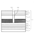
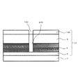
- the nitride-based compound semiconductor according to the first embodiment of the present invention includes a substrate 1 and a nitride-based compound semiconductor stacked body 11 stacked on the substrate 1.
- the nitride compound semiconductor may be an epitaxial wafer, for example.
- the substrate 1 is, for example, a boron-doped CZSi substrate of 0.01 ⁇ ⁇ cm.
- the substrate 1 may be any substrate that can be used for epitaxial growth of a nitride-based compound semiconductor.
- a Si substrate, a SiC substrate, a GaN substrate, and a sapphire substrate can be used.
- the nitride-based compound semiconductor stack 11 includes an initial growth layer 2, a composition gradient buffer layer 3, a multilayer buffer layer 4, a GaN channel layer 5, and an electron supply layer 6.
- the buffer layer 3, the multilayer buffer layer 4, the GaN channel layer 5, and the electron supply layer 6 are stacked in this order.
- the initial growth layer 2 is made of, for example, AlN having a thickness of 100 nm.
- the composition gradient buffer layer 3 includes an Al 0.7 Ga 0.3 N layer 31, an Al 0.4 Ga 0.6 N layer 32, and an Al 0.1 Ga 0.9 N layer 33, and is initially grown.
- the Al composition ratio of the Al 0.7 Ga 0.3 N layer 31, the Al 0.4 Ga 0.6 N layer 32, and the Al 0.1 Ga 0.9 N layer 33 is decreased stepwise. It has the structure laminated
- the Al 0.7 Ga 0.3 N layer 31 has a thickness of 200 nm, for example, and the Al 0.4 Ga 0.6 N layer 32 has a thickness of 400 nm, for example, and an Al 0.1 Ga 0.9 N layer. 33 has a thickness of 400 nm, for example.
- Multilayer buffer layer 4 Al x In y Ga 1- x-y As u P v N 1-u-v (0 ⁇ x ⁇ 1,0 ⁇ y ⁇ 1, x + y ⁇ 1,0 ⁇ u ⁇ 1,0
- An AlN layer as a first layer having a composition of ⁇ v ⁇ 1, u + v ⁇ 1, and Al a In b Ga 1 -ab As c Pd N 1-cd (0 ⁇ a ⁇ 1,
- an Al 0.1 Ga 0.9 N layer as a second layer having a composition of 0 ⁇ b ⁇ 1, a + b ⁇ 1, 0 ⁇ c ⁇ 1, 0 ⁇ d ⁇ 1, c + d ⁇ 1),
- the first and second layers are alternately stacked a plurality of times.
- the AlN layer is, for example, 3 nm thick, and the Al 0.1 Ga 0.9 N layer is, for example, 30 nm thick.
- the multilayer buffer layer has a configuration in which a plurality of layers having different compositions are repeatedly stacked, and each layer constituting the multilayer buffer layer has a composition formula of Al x In y Ga 1-xy As.
- u P v N 1-uv (0 ⁇ x ⁇ 1, 0 ⁇ y ⁇ 1, x + y ⁇ 1, 0 ⁇ u ⁇ 1, 0 ⁇ v ⁇ 1, u + v ⁇ 1) It may be a lattice buffer layer.
- the multilayer buffer layer 4 is not limited to a configuration in which the first and second layers are alternately and repeatedly stacked.
- the multilayer buffer layer 4 may have a configuration in which the first and second layers are randomly stacked.
- a configuration including a region in which the first and second layers are alternately and repeatedly stacked and a region in which the first and second layers are randomly stacked may be employed.
- the GaN channel layer 5 is made of, for example, GaN having a thickness of 1 ⁇ m.
- the electron supply layer 6 includes an AlN characteristic improving layer 61, an AlGaN barrier layer 62, and a GaN cap layer 63.
- the AlN characteristic improving layer 61, the AlGaN barrier layer 62, and the GaN cap layer 63 are provided on the GaN channel layer 5, the AlN characteristic improving layer 61, the AlGaN barrier layer 62, and the GaN cap layer 63 are provided. It has the structure laminated
- the AlN characteristic improving layer 61 is, for example, 1 nm in thickness
- the AlGaN barrier layer 62 is, for example, 20 nm thick Al 0.2 Ga 0.8 N
- the GaN cap layer 63 is, for example, 1 nm thick.
- the nitride-based compound semiconductor multilayer body 11 has a recess 110 that penetrates the electron supply layer 6, the GaN channel layer 5, and the multilayer buffer layer 4 from the surface of the electron supply layer 6 to the composition gradient buffer layer 3.
- a heat dissipation layer 210 adjacent to the multilayer buffer layer 4 and the GaN channel layer 5 is provided in the recess 110.
- the heat dissipation layer 210 is made of GaN having higher thermal conductivity than the multilayer buffer layer 4 and excellent heat dissipation, and is formed so that the multilayer buffer layer 4 and the GaN channel layer 5 are not exposed in the recess 110.
- the recess 110 is formed in a portion that does not contribute to the operation of this device, for example, an isolation portion, when a nitride compound semiconductor device is used.
- the surface oxide film of the substrate 1 is removed with a hydrofluoric acid-based etchant. Thereafter, the substrate 1 is set in a metal organic chemical vapor deposition (MOCVD) apparatus, the temperature of the substrate 1 is set to 1100 ° C., and the surface of the substrate 1 is cleaned at a chamber pressure of 13.3 kPa.
- MOCVD metal organic chemical vapor deposition
- the surface of the substrate 1 is nitrided by making the temperature of the substrate 1 and the chamber pressure constant and flowing ammonia NH 3 (12.5 slm).
- the temperature of the substrate 1 is set to 1150 ° C.
- the composition gradient buffer layer 3 is formed by growing the N layer 33.
- an AlN characteristic improving layer 61 (thickness 1 nm), an Al 0.2 Ga 0.8 N barrier layer 62 (thickness 20 nm), and a GaN cap layer 63 (thickness 1 nm) are formed on the GaN channel layer 5.
- the electron supply layer 6 is formed by sequentially growing the layers.
- the multilayer buffer layer 4, the GaN channel layer 5, and the electron supply layer 6 are etched to form a recess 110, and a heat dissipation layer 210 made of GaN is formed in the recess 110.
- Recess 110 may, for example, on the electron supply layer 6 is deposited SiO 2 by a sputtering apparatus, to remove the SiO 2 region to the heat dissipation layer 210 formed so as regions that do not form a heat dissipation layer 210 is covered with SiO 2 It is formed by patterning and dry etching by RIE using fluorine gas. The deposited SiO 2 is removed after the heat radiation layer 210 is formed.
- the nitride-based compound semiconductor according to the first embodiment has a recess 110 that reaches the composition gradient buffer layer 3 from the surface of the electron supply layer 6 through the electron supply layer 6, the GaN channel layer 5, and the multilayer buffer layer 4.
- the multilayer buffer layer 4 and the GaN channel layer 5 stacked on the multilayer buffer layer 4 are adjacent to each other, and the thermal conductivity in the vertical direction of the substrate 1 is higher than that of the multilayer buffer layer 4.
- High heat dissipation layer 210 is provided.
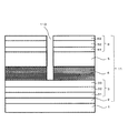
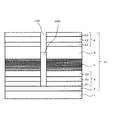
- the nitride-based compound semiconductor of the second embodiment includes an electron supply layer 6, a GaN channel layer, and a nitride-based compound semiconductor multilayer body 11 of the first embodiment, from the surface of the electron supply layer 6. 5.
- a recess 120 that penetrates the multilayer buffer layer 4 and the composition gradient buffer layer 3 to reach the initial growth layer 2 is provided, and a heat dissipation layer 220 made of GaN is provided in the recess 120.
- the same number is attached
- the heat dissipation layer 220 is adjacent to the GaN channel layer 5, the multilayer buffer layer 4, and the composition gradient buffer layer 3, and is formed so that the GaN channel layer 5, the multilayer buffer layer 4, and the composition gradient buffer layer 3 are not exposed in the recess 120.
- the recess 120 is formed in a portion (such as an isolation portion) that does not contribute to the operation of the nitride-based compound semiconductor device.
- the nitride-based compound semiconductor of the second embodiment can be manufactured, for example, by the same method as the nitride-based compound semiconductor of the first embodiment.
- the nitride-based compound semiconductor of the second embodiment from the surface of the electron supply layer 6 to the initial growth layer 2 through the electron supply layer 6, the GaN channel layer 5, the multilayer buffer layer 4, and the composition gradient buffer layer 3.
- a recessed portion 120 is provided, and a heat dissipation layer 220 is provided in the recessed portion 120.
- the initial growth layer 2 made of AlN becomes an etch stop layer, and reproducible and stable etching becomes possible.
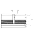
- the nitride-based compound semiconductor according to the third embodiment includes a substrate 1 and a nitride-based compound semiconductor stacked body 13 stacked on the substrate 1.
- the nitride-based compound semiconductor stacked body 13 includes an initial growth layer 2, a multilayer buffer layer 4, a GaN channel layer 5, and an electron supply layer 106, and the initial growth layer 2, multilayer buffer layer 4, and GaN channel layer 5. And an electron supply layer 106 are sequentially stacked.
- the same number is attached
- the electron supply layer 106 is made of, for example, an Al 0.22 Ga 0.78 N barrier layer having a thickness of 25 nm.
- the initial growth layer 2 has a thickness of 120 nm, and an AlN layer (thickness 5 nm) / Al 0.1 Ga 0.9 N layer (thickness 30 nm) is repeatedly grown to obtain a multilayer.
- the buffer layer 4 is formed, and the thickness of the GaN channel layer 5 is 1.5 nm.
- the nitride-based compound semiconductor stacked body 13 is provided with a recess 130 that penetrates the electron supply layer 106, the GaN channel layer 5, and the multilayer buffer layer 4 from the surface of the electron supply layer 106 to the initial growth layer 2. .
- a heat dissipation layer 210 made of GaN adjacent to the multilayer buffer layer 4 and the GaN channel layer 5 is provided in the recess 130.
- the recess 130 is formed in a portion (such as an isolation portion) that does not contribute to the operation of the nitride-based compound semiconductor device.
- the surface oxide film of the substrate 1 is removed with a hydrofluoric acid-based etchant. Thereafter, the substrate 1 is set in a metal organic chemical vapor deposition (MOCVD) apparatus, the temperature of the substrate 1 is set to 1100 ° C., and the surface of the substrate 1 is cleaned at a chamber pressure of 13.3 kPa.
- MOCVD metal organic chemical vapor deposition
- the surface of the substrate 1 is nitrided by making the temperature of the substrate 1 and the chamber pressure constant and flowing ammonia NH 3 (12.5 slm).
- SiO 2 is deposited on the initial growth layer 2 by a sputtering apparatus to remove the SiO 2 in the region where the heat dissipation layer 210 is grown, and the region where the multilayer buffer layer 4 is grown is covered with SiO 2 . Then, the heat dissipation layer 210 is formed by patterning. After the heat radiation layer 210 is formed, SiO 2 is removed.
- SiO 2 is deposited on the heat dissipation layer 210 by a sputtering apparatus and patterned so that only the surface of the heat dissipation layer 210 is covered with SiO 2 , and then an AlN layer (thickness 3 nm) / Al 0.1
- a multilayer buffer layer 4 is formed on the initial growth layer 2 by repeatedly growing a Ga 0.9 N layer (thickness 30 nm). Then, a GaN channel layer 5 having a thickness of 1.5 ⁇ m and an electron supply layer 106 made of a 25 nm thick Al 0.22 Ga 0.78 N barrier layer are sequentially grown on the multilayer buffer layer 4, and then a heat dissipation layer The SiO 2 covering the surface of 210 is removed.
- the multilayer buffer layer 4 is stacked on the initial growth layer 2, and the electron supply layer 106 is formed of an Al 0.22 Ga 0.78 N barrier layer. For this reason, the temperature rise of the GaN channel layer 5 can be suppressed with a simple structure, and the cost can be reduced.
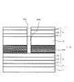
- the nitride-based compound semiconductor according to the fourth embodiment includes a substrate 1 and a nitride-based compound semiconductor stacked body 14 stacked on the substrate 1.
- the nitride-based compound semiconductor stack 14 includes an initial growth layer 102, a multilayer buffer layer 4, a GaN channel layer 5, and an electron supply layer 6, and the initial growth layer 102, the multilayer buffer layer 4, and the GaN channel layer 5. And the electron supply layer 6 are sequentially stacked.
- the same components as those in the first to third embodiments are denoted by the same reference numerals, and the description of the first to third embodiments is cited.
- the initial growth layer 102 is made of GaN grown at a low temperature, and has a layer thickness of, for example, 50 nm.
- a layer thickness of, for example, 50 nm.
- an AlN layer (thickness 3 nm) / Al 0.1 Ga 0.9 N layer (thickness 25 nm) is repeatedly grown to form the multilayer buffer layer 4 and the GaN channel layer 5.
- the thickness is 1.5 nm.
- the nitride compound semiconductor stacked body 14 is provided with a recess 140 that extends from the surface of the electron supply layer 6 to the initial growth layer 102 through the electron supply layer 6, the GaN channel layer 5, and the multilayer buffer layer 4. .
- the recess 140 is formed in a portion (such as an isolation portion) that does not contribute to the operation of the nitride-based compound semiconductor device.
- a heat dissipation layer 210 made of GaN adjacent to the multilayer buffer layer 4 and the GaN channel layer 5 is provided.
- the nitride-based compound semiconductor of the fourth embodiment can be manufactured, for example, by the same method as the nitride-based compound semiconductor of the third embodiment.
- the initial growth layer 102 can be made of GaN
- a substrate and a structure suitable for the initial growth layer 102 made of GaN can be used.
- the nitride-based compound semiconductor according to the fifth embodiment includes a substrate 1 and a nitride-based compound semiconductor stacked body 15 stacked on the substrate 1.
- the nitride-based compound semiconductor stacked body 15 includes an initial growth layer 2, a composition gradient buffer layer 103, a multilayer buffer layer 4, a GaN channel layer 5, and an electron supply layer 106.
- the buffer layer 103, the multilayer buffer layer 4, the GaN channel layer 5, and the electron supply layer 106 are stacked in this order.
- the same number is attached
- the composition gradient buffer layer 103 includes an Al 0.7 Ga 0.3 N layer 31, an Al 0.5 Ga 0.5 N layer 34, an Al 0.3 Ga 0.7 N layer 35, and an Al 0.1 layer. It is composed of a Ga 0.9 N layer 33, and has a structure in which the Al composition is stacked on the initial growth layer 2 so that the Al composition is gradually reduced.
- the Al 0.7 Ga 0.3 N layer 31 has a thickness of 200 nm, for example, and the Al 0.5 Ga 0.5 N layer 34 has a thickness of 200 nm, for example, and an Al 0.3 Ga 0.7 N layer.
- 35 has a thickness of 300 nm, for example, and the Al 0.1 Ga 0.9 N layer 33 has a thickness of 400 nm, for example.
- the nitride compound semiconductor multilayer body 15 is provided with a recess 150 that extends from the surface of the electron supply layer 106 through the electron supply layer 106, the GaN channel layer 5, and the multilayer buffer layer 4 to the composition gradient buffer layer 103. Yes.
- a heat dissipation layer 210 made of GaN adjacent to the multilayer buffer layer 4 and the GaN channel layer 5 is provided.
- the nitride-based compound semiconductor of the fifth embodiment can be manufactured, for example, by the same method as the nitride-based compound semiconductor of the first embodiment.
- the Al 0.7 Ga 0.3 N layer 31, the Al 0.5 Ga 0.5 N layer 34, the Al 0.3 Ga 0.7 N layer 35, and The composition gradient buffer layer 103 is formed by sequentially stacking Al 0.1 Ga 0.9 N layers 33. For this reason, the warp of the nitride-based compound semiconductor can be controlled in detail.
- the nitride-based compound semiconductor according to the sixth embodiment includes a substrate 1 and a nitride-based compound semiconductor stacked body 16 stacked on the substrate 1.
- the nitride-based compound semiconductor stack 16 includes an initial growth layer 2, a composition gradient buffer layer 3, a multilayer buffer layer 104, a GaN channel layer 5, and an electron supply layer 6.
- the buffer layer 3, the multilayer buffer layer 104, the GaN channel layer 5, and the electron supply layer 6 are stacked in this order.
- the same components as those in the first to fifth embodiments are denoted by the same reference numerals, and the description of the first to fifth embodiments is cited.
- the multilayer buffer layer 104 includes an AlN layer as a first layer, an Al 0.1 Ga 0.9 N layer as a second layer, and an Al 0.5 Ga 0.5 N layer as a third layer. And the Al 0.5 Ga 0.5 N layer / AlN layer / Al 0.1 Ga 0.9 N layer is repeatedly laminated on the composition gradient buffer layer 3.
- the AlN layer is, for example, 3 nm thick
- the Al 0.1 Ga 0.9 N layer is, for example, 25 nm thick
- the Al 0.5 Ga 0.5 N layer for example, is 5 nm thick.
- the nitride-based compound semiconductor stacked body 16 is provided with a recess 160 that penetrates the electron supply layer 6, the GaN channel layer 5, and the multilayer buffer layer 104 from the surface of the electron supply layer 6 to the composition gradient buffer layer 3. Yes. And in this recessed part 160, the thermal radiation layer 260 which consists of GaN is provided.
- the heat dissipation layer 260 is adjacent to the GaN channel layer 5 and the multilayer buffer layer 104 and is formed so that the GaN channel layer 5 and the multilayer buffer layer 104 are not exposed in the recess 160.
- the nitride-based compound semiconductor according to the sixth embodiment can be manufactured, for example, by the same method as the nitride-based compound semiconductor according to the first embodiment.
- the nitride-based compound semiconductor according to the sixth embodiment includes an Al 0.5 Ga 0.5 N layer / AlN layer / Al 0.1 Ga 0.9 N layer obtained by repeatedly growing the multilayer buffer layer 104 a plurality of times. ing. Therefore, the crystallinity of the multilayer buffer layer 104 can be improved.
- the nitride-based compound semiconductor of the seventh embodiment is formed in the GaN channel layer 5 and the multilayer buffer layer 4 in the recess 130 provided in the nitride-based compound semiconductor stack 13 of the third embodiment.
- An adjacent heat dissipation layer 270 is provided.
- the same number is attached
- the heat dissipation layer 270 is made of AlN having a higher thermal conductivity than GaN (the thermal conductivity of AlN is 2.9 W / cm ⁇ K, the thermal conductivity of GaN is 1.3 W / cm ⁇ K), and the GaN channel
- the layer 5 and the multilayer buffer layer 4 are formed so as not to be exposed in the recess 130.
- the nitride-based compound semiconductor of the seventh embodiment can be manufactured by, for example, the same method as the nitride-based compound semiconductor of the third embodiment.
- the heat dissipation layer 270 is made of AlN having a higher thermal conductivity than GaN, the temperature increase of the GaN channel layer 5 can be reliably suppressed.
- the nitride-based compound semiconductor according to the eighth embodiment has a heat dissipation layer 280 made of GaN in the recess 120 provided in the nitride-based compound semiconductor multilayer body 11 according to the second embodiment. It is.
- the same components as those in the first to seventh embodiments are denoted by the same reference numerals, and the description of the first to seventh embodiments is incorporated.
- the heat dissipation layer 280 is adjacent to the GaN channel layer 5, the multilayer buffer layer 4, and the composition gradient buffer layer 3, and is formed so that a part of the GaN channel layer 5 is exposed in the recess 120.
- the nitride-based compound semiconductor of the eighth embodiment can be manufactured, for example, by the same method as the nitride-based compound semiconductor of the first embodiment.
- the heat dissipation layer 280 is provided so that a part of the GaN channel layer 5 is exposed in the recess 120, it flows through the interface between the heat dissipation layer 280 and the GaN channel layer 5. Leakage current can be suppressed.
- the GaN channel layer 5 is laminated on the multilayer buffer layers 4 and 104, but the present invention is not limited to this.
- an AlN layer may be provided between the multilayer buffer layer and the GaN channel layer. Thereby, the curvature of the nitride compound semiconductor can be controlled.
- the heat radiation layers 210, 220, 260, 270, and 280 may be adjacent to the multilayer buffer layer 4, 104 and at least a part of the layers stacked on the multilayer buffer layer 4, 104.
- the interface between the heat dissipation layers 210, 220, 260, 270, 280 and the GaN channel layer 5 is provided. The flowing leak current can be reduced.
- the nitride compound semiconductor of the present invention is Substrate 1; A nitride-based compound semiconductor multilayer body 11, 12, 13, 14, 15, 16 provided on the substrate 1;
- the nitride-based compound semiconductor stacked body 11, 12, 13, 14, 15, 16 includes a multilayer buffer layer 4, 104, a channel layer 5 provided on the multilayer buffer layer 4, 104, and the channel layer 5
- Recesses 110, 120, 130, 140, 150, 160 penetrating the channel layer 5 and the multilayer buffer layers 4, 104 from the surface of the electron supply layers 6, 106, In the recesses 110, 120, 130, 140, 150, 160, the multilayer buffer layer 4, 104, adjacent to the multilayer buffer layer 4, and the layer 5 laminated on the multilayer buffer layer 4, 104, and the multilayer buffer layer
- the heat-dissipating layer 210, 220, 260, 270, 280 having a higher thermal conductivity than 4,104 is provided
- heat radiation layers 210, 220, 260, 270, 280 having higher thermal conductivity than the multilayer buffer layers 4, 104 are provided.
- the multilayer buffer layers 4 and 104 are formed of Al x In y Ga 1-xy As u P v N 1-uv (0 ⁇ x ⁇ 1, 0 ⁇ y ⁇ 1, x + y ⁇ 1, 0 ⁇ u ⁇ A first layer having a composition of 1, 0 ⁇ v ⁇ 1, u + v ⁇ 1), and Al a In b Ga 1-ab As c Pd N 1-cd (0 ⁇ a ⁇ 1, 0 ⁇ b ⁇ 1, a + b ⁇ 1, 0 ⁇ c ⁇ 1, 0 ⁇ d ⁇ 1, c + d ⁇ 1).
- the heat conducted from the surface of the electron supply layers 6, 106 toward the multilayer buffer layers 4, 104 passes through the heat dissipation layers 210, 220, 260, 270, 280 of the nitride compound semiconductor. Since it is released to the outside, the heat dissipation of the nitride-based compound semiconductor including the multilayer buffer layers 4 and 104 having a low thermal conductivity in the vertical direction of the substrate 1 can be improved. Therefore, by using the nitride-based compound semiconductor for a semiconductor electronic device, it is possible to obtain a highly reliable semiconductor electronic device including improvement in short-circuit tolerance.
- the multilayer buffer layers 4 and 104 are stacked on the composition gradient buffer layers 3 and 103 formed of a plurality of AlGaN layers that are stacked so that the Al composition is sequentially reduced.
- the crystallinity of the multilayer buffer layers 4 and 104 can be increased, and the warpage of the nitride-based compound semiconductor can be controlled. it can.
- the heat dissipation layer 210,220,260,270,280 are, Al x In y Ga 1- x-y As u P v N 1-u-v (0 ⁇ x ⁇ 1,0 ⁇ y ⁇ 1, x + y ⁇ 1 , 0 ⁇ u ⁇ 1, 0 ⁇ v ⁇ 1, u + v ⁇ 1).
- the composition of the heat dissipation layers 210, 220, 260, 270, 280 approximates the composition of the multilayer buffer layer 4, 104, the heat dissipation layers 210, 220, 260, 270, 280 by epitaxial growth are used. Easy to grow.
- composition gradient buffer layers 3 and 103 are composed of two to four AlGaN layers.
- the warpage of the nitride-based compound semiconductor can be controlled in detail.
- the substrate 1 is a Si substrate.
- the heat dissipation is high, and it can be manufactured at low cost.
- the thickness, composition, and formation process of each layer constituting the nitride-based compound semiconductor multilayer body 11, 13, 14, 15, 16 are the same as for the nitride-based compound. It can be changed as appropriate according to the design of the semiconductor or the warpage adjustment of the wafer.
Landscapes
- Junction Field-Effect Transistors (AREA)
- Chemical & Material Sciences (AREA)
- Composite Materials (AREA)
- Engineering & Computer Science (AREA)
- Materials Engineering (AREA)
- Recrystallisation Techniques (AREA)
Abstract
Description
基板と、
上記基板上に設けられた窒化物系化合物半導体積層体と
を備え、
上記窒化物系化合物半導体積層体が、多層バッファ層と、この多層バッファ層上に設けられたチャネル層と、このチャネル層上に積層された電子供給層とを含んでいる窒化物系化合物半導体において、
上記電子供給層の表面から、上記チャネル層および上記多層バッファ層を貫通する凹部を有し、
上記凹部内に、上記多層バッファ層、および、この多層バッファ層上に積層された層に隣接し、かつ、上記多層バッファ層よりも熱伝導率の高い放熱層が設けられていることを特徴としている。
本発明の第1実施形態の窒化物系化合物半導体は、図1に示すように、基板1と、この基板1上に積層された窒化物系化合物半導体積層体11とを備えている。なお、窒化物系化合物半導体は、例えばエピタキシャルウェハでもよい。
・TMG流量=57μmol/min、TMA流量=97μmol/min、NH3流量=12.5slmとして、初期成長層2上に、厚さ200nmのAl0.7Ga0.3N層31を成長させ、
・TMG流量=99μmol/min、TMA流量=55μmol/min、NH3流量=12.5slmとして、Al0.7Ga0.3N層31上に、厚さ400nmのAl0.4Ga0.6N層32を成長させ、
・TMG流量=137μmol/min、TMA流量=18μmol/min、NH3流量=12.5slmとして、Al0.4Ga0.6N層32上に、厚さ400nmのAl0.1Ga0.9N層33を成長させて、組成傾斜バッファ層3を形成する。
第2実施形態の窒化物系化合物半導体は、図4に示すように、第1実施形態の窒化物系化合物半導体積層体11に、電子供給層6の表面から、電子供給層6、GaNチャネル層5、多層バッファ層4および組成傾斜バッファ層3を貫通して、初期成長層2まで達する凹部120を設け、この凹部120内にGaNからなる放熱層220を設けたものである。なお、上記第1実施形態と同一の構成部には同一番号を付しており、第1実施形態の説明を援用する。
第3実施形態の窒化物系化合物半導体は、図5に示すように、基板1と、この基板1上に積層された窒化物系化合物半導体積層体13とを備えている。窒化物系化合物半導体積層体13は、初期成長層2と、多層バッファ層4と、GaNチャネル層5と、電子供給層106とからなり、初期成長層2、多層バッファ層4、GaNチャネル層5および電子供給層106を順に積層した構成を有している。なお、上記第1,第2実施形態と同一の構成部には同一番号を付しており、第1,第2実施形態の説明を援用する。
第4実施形態の窒化物系化合物半導体は、図6に示すように、基板1と、この基板1上に積層された窒化物系化合物半導体積層体14とを備えている。窒化物系化合物半導体積層体14は、初期成長層102と、多層バッファ層4と、GaNチャネル層5と、電子供給層6とからなり、初期成長層102、多層バッファ層4、GaNチャネル層5および電子供給層6を順に積層した構成を有している。なお、上記第1~第3実施形態と同一の構成部には同一番号を付しており、第1~第3実施形態の説明を援用する。
第5実施形態の窒化物系化合物半導体は、図7に示すように、基板1と、この基板1上に積層された窒化物系化合物半導体積層体15とを備えている。窒化物系化合物半導体積層体15は、初期成長層2と、組成傾斜バッファ層103と、多層バッファ層4と、GaNチャネル層5と、電子供給層106とからなり、初期成長層2、組成傾斜バッファ層103、多層バッファ層4、GaNチャネル層5および電子供給層106を順に積層した構成を有している。なお、上記第1~第4実施形態と同一の構成部には同一番号を付しており、第1~第4実施形態の説明を援用する。
第6実施形態の窒化物系化合物半導体は、図8に示すように、基板1と、この基板1上に積層された窒化物系化合物半導体積層体16とを備えている。窒化物系化合物半導体積層体16は、初期成長層2と、組成傾斜バッファ層3と、多層バッファ層104と、GaNチャネル層5と、電子供給層6とからなり、初期成長層2、組成傾斜バッファ層3、多層バッファ層104、GaNチャネル層5および電子供給層6を順に積層した構成を有している。なお、上記第1~第5実施形態と同一の構成部には同一番号を付しており、第1~第5実施形態の説明を援用する。
第7実施形態の窒化物系化合物半導体は、図9に示すように、第3実施形態の窒化物系化合物半導体積層体13に設けた凹部130内に、GaNチャネル層5および多層バッファ層4に隣接する放熱層270を設けたものである。なお、上記第1~第6実施形態と同一の構成部には同一番号を付しており、第1~第6実施形態の説明を援用する。
第8実施形態の窒化物系化合物半導体は、図10に示すように、第2実施形態の窒化物系化合物半導体積層体11に設けた凹部120内に、GaNからなる放熱層280を設けたものである。なお、上記第1~第7実施形態と同一の構成部には同一番号を付しており、第1~第7実施形態の説明を援用する。
基板1と、
上記基板1上に設けられた窒化物系化合物半導体積層体11,12,13,14,15,16と
を有し、
上記窒化物系化合物半導体積層体11,12,13,14,15,16が、多層バッファ層4,104と、この多層バッファ層4,104上に設けられたチャネル層5と、このチャネル層5上に積層された電子供給層6,106と、を含んでいる窒化物系化合物半導体において、
上記電子供給層6,106の表面から、上記チャネル層5および上記多層バッファ層4,104を貫通する凹部110,120,130,140,150,160を有し、
上記凹部110,120,130,140,150,160内に、上記多層バッファ層4,104、および、この多層バッファ層4,104上に積層された層5に隣接し、かつ、上記多層バッファ層4,104よりも熱伝導率の高い放熱層210,220,260,270,280が設けられていることを特徴としている。
上記多層バッファ層4,104が、AlxInyGa1-x-yAsuPvN1-u-v(0≦x≦1、0≦y≦1、x+y≦1、0≦u<1、0≦v<1、u+v<1)の組成を有する第1の層と、AlaInbGa1-a-bAscPdN1-c-d(0≦a≦1、0≦b≦1、a+b≦1、0≦c<1、0≦d<1、c+d<1)の組成を有する第2の層とを含んでいる。
上記多層バッファ層4,104が、Al組成が段階的に順次低減されるように積層されている複数のAlGaN層で構成された組成傾斜バッファ層3,103上に積層されている。
できる。
上記放熱層210,220,260,270,280が、AlxInyGa1-x-yAsuPvN1-u-v(0≦x≦1、0≦y≦1、x+y≦1、0≦u<1、0≦v<1、u+v<1)の組成を有している。
上記組成傾斜バッファ層3,103が、2層から4層のAlGaN層で構成されている。
上記基板1が、Si基板である。
2,102 初期成長層
3,103 組成傾斜バッファ層
4,104 多層バッファ層
5 GaNチャネル層
6,106 電子供給層
11,13,14,15,16 窒化物系化合物半導体積層体
110,120,130,140,150,160 凹部
210,220,260,270,280 放熱層
Claims (6)
- 基板(1)と、
上記基板(1)上に設けられた窒化物系化合物半導体積層体(11,12,13,14,15,16)と
を備え、
上記窒化物系化合物半導体積層体(11,12,13,14,15,16)が、多層バッファ層(4,104)と、この多層バッファ層(4,104)上に設けられたチャネル層(5)と、このチャネル層(5)上に積層された電子供給層(6,106)とを含んでいる窒化物系化合物半導体において、
上記電子供給層(6,106)の表面から、上記チャネル層(5)および上記多層バッファ層(4,104)を貫通する凹部(110,120,130,140,150,160)を有し、
上記凹部(110,120,130,140,150,160)内に、上記多層バッファ層(4,104)、および、この多層バッファ層(4,104)上に積層された層に隣接し、かつ、上記多層バッファ層(4,104)よりも熱伝導率の高い放熱層(210,220,260,270,280)が設けられていることを特徴とする窒化物系化合物半導体。 - 請求項1に記載の窒化物系化合物半導体において、
上記多層バッファ層(4,104)が、AlxInyGa1-x-yAsuPvN1-u-v(0≦x≦1、0≦y≦1、x+y≦1、0≦u<1、0≦v<1、u+v<1)の組成を有する第1の層と、AlaInbGa1-a-bAscPdN1-c-d(0≦a≦1、0≦b≦1、a+b≦1、0≦c<1、0≦d<1、c+d<1)の組成を有する第2の層とを含んでいることを特徴とする窒化物系化合物半導体。 - 請求項1または2に記載の窒化物系化合物半導体において、
上記多層バッファ層(4,104)が、Al組成が段階的に順次低減されるように積層されている複数のAlGaN層で構成された組成傾斜バッファ層(3,103)上に積層されていることを特徴とする窒化物系化合物半導体。 - 請求項3に記載の窒化物系化合物半導体において、
上記組成傾斜バッファ層(3,103)が、2層から4層のAlGaN層で構成されていることを特徴とする窒化物系化合物半導体。 - 請求項1から4のいずれか1つに記載の窒化物系化合物半導体において、
上記放熱層(210,220,260,270,280)が、AlxInyGa1-x-yAsuPvN1-u-v(0≦x≦1、0≦y≦1、x+y≦1、0≦u<1、0≦v<1、u+v<1)の組成を有していることを特徴とする窒化物系化合物半導体。 - 請求項1から5のいずれか1つに記載の窒化物系化合物半導体において、
上記基板(1)が、Si基板であることを特徴とする窒化物系化合物半導体。
Priority Applications (3)
| Application Number | Priority Date | Filing Date | Title |
|---|---|---|---|
| CN201580027209.XA CN106415802B (zh) | 2014-05-26 | 2015-04-17 | 氮化物类化合物半导体 |
| US15/127,642 US9773864B2 (en) | 2014-05-26 | 2015-04-17 | Nitride compound semiconductor |
| JP2016523378A JP6174253B2 (ja) | 2014-05-26 | 2015-04-17 | 窒化物系化合物半導体 |
Applications Claiming Priority (2)
| Application Number | Priority Date | Filing Date | Title |
|---|---|---|---|
| JP2014-108159 | 2014-05-26 | ||
| JP2014108159 | 2014-05-26 |
Publications (1)
| Publication Number | Publication Date |
|---|---|
| WO2015182283A1 true WO2015182283A1 (ja) | 2015-12-03 |
Family
ID=54698624
Family Applications (1)
| Application Number | Title | Priority Date | Filing Date |
|---|---|---|---|
| PCT/JP2015/061860 Ceased WO2015182283A1 (ja) | 2014-05-26 | 2015-04-17 | 窒化物系化合物半導体 |
Country Status (4)
| Country | Link |
|---|---|
| US (1) | US9773864B2 (ja) |
| JP (1) | JP6174253B2 (ja) |
| CN (1) | CN106415802B (ja) |
| WO (1) | WO2015182283A1 (ja) |
Families Citing this family (2)
| Publication number | Priority date | Publication date | Assignee | Title |
|---|---|---|---|---|
| WO2021134479A1 (zh) * | 2019-12-31 | 2021-07-08 | 苏州晶湛半导体有限公司 | 一种半导体结构及其制备方法 |
| CN116097450A (zh) * | 2020-09-21 | 2023-05-09 | 华为技术有限公司 | 晶体管器件及电子装置 |
Citations (4)
| Publication number | Priority date | Publication date | Assignee | Title |
|---|---|---|---|---|
| JP2010028038A (ja) * | 2008-07-24 | 2010-02-04 | Sharp Corp | ヘテロ接合電界効果トランジスタ |
| JP2011192882A (ja) * | 2010-03-16 | 2011-09-29 | Nec Corp | 半導体構造及び半導体装置及びその製造方法 |
| JP2012038885A (ja) * | 2010-08-06 | 2012-02-23 | Panasonic Corp | 半導体装置及びその製造方法 |
| JP2013026321A (ja) * | 2011-07-19 | 2013-02-04 | Sharp Corp | 窒化物系半導体層を含むエピタキシャルウエハ |
Family Cites Families (9)
| Publication number | Priority date | Publication date | Assignee | Title |
|---|---|---|---|---|
| US7233028B2 (en) * | 2001-02-23 | 2007-06-19 | Nitronex Corporation | Gallium nitride material devices and methods of forming the same |
| JP2003059948A (ja) | 2001-08-20 | 2003-02-28 | Sanken Electric Co Ltd | 半導体装置及びその製造方法 |
| JP3960957B2 (ja) | 2003-09-05 | 2007-08-15 | 古河電気工業株式会社 | 半導体電子デバイス |
| JP2007157829A (ja) * | 2005-12-01 | 2007-06-21 | Matsushita Electric Ind Co Ltd | 半導体装置 |
| JP2008078486A (ja) * | 2006-09-22 | 2008-04-03 | Oki Electric Ind Co Ltd | 半導体素子 |
| US8039301B2 (en) * | 2007-12-07 | 2011-10-18 | The United States Of America As Represented By The Secretary Of The Navy | Gate after diamond transistor |
| WO2010131451A1 (ja) * | 2009-05-11 | 2010-11-18 | Dowaエレクトロニクス株式会社 | 電子デバイス用エピタキシャル基板およびその製造方法 |
| JP5604855B2 (ja) * | 2009-11-17 | 2014-10-15 | 富士通株式会社 | 半導体装置及びその製造方法 |
| JP5754452B2 (ja) * | 2013-03-08 | 2015-07-29 | 富士通株式会社 | 半導体装置の製造方法 |
-
2015
- 2015-04-17 CN CN201580027209.XA patent/CN106415802B/zh active Active
- 2015-04-17 JP JP2016523378A patent/JP6174253B2/ja active Active
- 2015-04-17 US US15/127,642 patent/US9773864B2/en active Active
- 2015-04-17 WO PCT/JP2015/061860 patent/WO2015182283A1/ja not_active Ceased
Patent Citations (4)
| Publication number | Priority date | Publication date | Assignee | Title |
|---|---|---|---|---|
| JP2010028038A (ja) * | 2008-07-24 | 2010-02-04 | Sharp Corp | ヘテロ接合電界効果トランジスタ |
| JP2011192882A (ja) * | 2010-03-16 | 2011-09-29 | Nec Corp | 半導体構造及び半導体装置及びその製造方法 |
| JP2012038885A (ja) * | 2010-08-06 | 2012-02-23 | Panasonic Corp | 半導体装置及びその製造方法 |
| JP2013026321A (ja) * | 2011-07-19 | 2013-02-04 | Sharp Corp | 窒化物系半導体層を含むエピタキシャルウエハ |
Also Published As
| Publication number | Publication date |
|---|---|
| CN106415802A (zh) | 2017-02-15 |
| US20170141187A1 (en) | 2017-05-18 |
| JP6174253B2 (ja) | 2017-08-02 |
| US9773864B2 (en) | 2017-09-26 |
| CN106415802B (zh) | 2019-07-02 |
| JPWO2015182283A1 (ja) | 2017-04-20 |
Similar Documents
| Publication | Publication Date | Title |
|---|---|---|
| JP5785103B2 (ja) | ヘテロ接合型電界効果トランジスタ用のエピタキシャルウエハ | |
| JP5572976B2 (ja) | 半導体装置 | |
| CN103094314B (zh) | 在硅衬底上生长iii-氮化物的新方法 | |
| JP6180401B2 (ja) | エピタキシャルウェーハ、半導体素子、エピタキシャルウェーハの製造方法、並びに、半導体素子の製造方法 | |
| CN107112242B (zh) | 电子器件用外延基板、电子器件、电子器件用外延基板的制造方法及电子器件的制造方法 | |
| JP5159858B2 (ja) | 窒化ガリウム系化合物半導体基板とその製造方法 | |
| JP2016512485A (ja) | 希土類酸化物/シリコン基板上で成長した、ain中間層を含むiii−n材料 | |
| JP5923242B2 (ja) | 化合物半導体装置及び化合物半導体装置の製造方法 | |
| JP6126906B2 (ja) | 窒化物半導体エピタキシャルウェハ | |
| CN113451467A (zh) | 含氮半导体元件 | |
| JP6173493B2 (ja) | 半導体素子用のエピタキシャル基板およびその製造方法 | |
| JP6239017B2 (ja) | 窒化物半導体基板 | |
| JP2016062987A (ja) | 半導体装置およびその製造方法 | |
| JP6174253B2 (ja) | 窒化物系化合物半導体 | |
| JP2015103665A (ja) | 窒化物半導体エピタキシャルウエハおよび窒化物半導体 | |
| JP6029538B2 (ja) | 半導体装置 | |
| JP6370501B2 (ja) | 半導体装置及び半導体装置の製造方法 | |
| KR102793200B1 (ko) | 에피택시 웨이퍼 및 그 제조 방법 | |
| WO2016039178A1 (ja) | 窒化物半導体積層構造及びそれを用いた電子デバイス | |
| CN104425659A (zh) | 单光子光源元件及其制造方法 |
Legal Events
| Date | Code | Title | Description |
|---|---|---|---|
| 121 | Ep: the epo has been informed by wipo that ep was designated in this application |
Ref document number: 15800025 Country of ref document: EP Kind code of ref document: A1 |
|
| ENP | Entry into the national phase |
Ref document number: 2016523378 Country of ref document: JP Kind code of ref document: A |
|
| WWE | Wipo information: entry into national phase |
Ref document number: 15127642 Country of ref document: US |
|
| NENP | Non-entry into the national phase |
Ref country code: DE |
|
| 122 | Ep: pct application non-entry in european phase |
Ref document number: 15800025 Country of ref document: EP Kind code of ref document: A1 |