WO2015181983A1 - 電力変換装置、発電システム、制御装置および制御方法 - Google Patents
電力変換装置、発電システム、制御装置および制御方法 Download PDFInfo
- Publication number
- WO2015181983A1 WO2015181983A1 PCT/JP2014/064532 JP2014064532W WO2015181983A1 WO 2015181983 A1 WO2015181983 A1 WO 2015181983A1 JP 2014064532 W JP2014064532 W JP 2014064532W WO 2015181983 A1 WO2015181983 A1 WO 2015181983A1
- Authority
- WO
- WIPO (PCT)
- Prior art keywords
- power
- command
- gain
- control unit
- supply voltage
- Prior art date
- Legal status (The legal status is an assumption and is not a legal conclusion. Google has not performed a legal analysis and makes no representation as to the accuracy of the status listed.)
- Ceased
Links
Images





Classifications
-
- G—PHYSICS
- G05—CONTROLLING; REGULATING
- G05F—SYSTEMS FOR REGULATING ELECTRIC OR MAGNETIC VARIABLES
- G05F1/00—Automatic systems in which deviations of an electric quantity from one or more predetermined values are detected at the output of the system and fed back to a device within the system to restore the detected quantity to its predetermined value or values, i.e. retroactive systems
- G05F1/66—Regulating electric power
- G05F1/67—Regulating electric power to the maximum power available from a generator, e.g. from solar cell
-
- G—PHYSICS
- G05—CONTROLLING; REGULATING
- G05F—SYSTEMS FOR REGULATING ELECTRIC OR MAGNETIC VARIABLES
- G05F1/00—Automatic systems in which deviations of an electric quantity from one or more predetermined values are detected at the output of the system and fed back to a device within the system to restore the detected quantity to its predetermined value or values, i.e. retroactive systems
- G05F1/10—Regulating voltage or current
-
- H—ELECTRICITY
- H02—GENERATION; CONVERSION OR DISTRIBUTION OF ELECTRIC POWER
- H02J—ELECTRIC POWER NETWORKS; CIRCUIT ARRANGEMENTS OR SYSTEMS FOR SUPPLYING OR DISTRIBUTING ELECTRIC POWER; SYSTEMS FOR STORING ELECTRIC ENERGY
- H02J3/00—Circuit arrangements for AC mains or AC distribution networks
- H02J3/38—Arrangements for feeding a single network from two or more generators or sources in parallel; Arrangements for feeding already energised networks from additional generators or sources in parallel
-
- H—ELECTRICITY
- H02—GENERATION; CONVERSION OR DISTRIBUTION OF ELECTRIC POWER
- H02J—ELECTRIC POWER NETWORKS; CIRCUIT ARRANGEMENTS OR SYSTEMS FOR SUPPLYING OR DISTRIBUTING ELECTRIC POWER; SYSTEMS FOR STORING ELECTRIC ENERGY
- H02J3/00—Circuit arrangements for AC mains or AC distribution networks
- H02J3/38—Arrangements for feeding a single network from two or more generators or sources in parallel; Arrangements for feeding already energised networks from additional generators or sources in parallel
- H02J3/381—Dispersed generators
-
- H—ELECTRICITY
- H02—GENERATION; CONVERSION OR DISTRIBUTION OF ELECTRIC POWER
- H02J—ELECTRIC POWER NETWORKS; CIRCUIT ARRANGEMENTS OR SYSTEMS FOR SUPPLYING OR DISTRIBUTING ELECTRIC POWER; SYSTEMS FOR STORING ELECTRIC ENERGY
- H02J2101/00—Supply or distribution of decentralised, dispersed or local electric power generation
- H02J2101/20—Dispersed power generation using renewable energy sources
- H02J2101/22—Solar energy
- H02J2101/24—Photovoltaics
- H02J2101/25—Photovoltaics involving maximum power point tracking control for photovoltaic sources
-
- H—ELECTRICITY
- H02—GENERATION; CONVERSION OR DISTRIBUTION OF ELECTRIC POWER
- H02M—APPARATUS FOR CONVERSION BETWEEN AC AND AC, BETWEEN AC AND DC, OR BETWEEN DC AND DC, AND FOR USE WITH MAINS OR SIMILAR POWER SUPPLY SYSTEMS; CONVERSION OF DC OR AC INPUT POWER INTO SURGE OUTPUT POWER; CONTROL OR REGULATION THEREOF
- H02M1/00—Details of apparatus for conversion
- H02M1/0067—Converter structures employing plural converter units, other than for parallel operation of the units on a single load
- H02M1/007—Plural converter units in cascade
-
- H—ELECTRICITY
- H02—GENERATION; CONVERSION OR DISTRIBUTION OF ELECTRIC POWER
- H02M—APPARATUS FOR CONVERSION BETWEEN AC AND AC, BETWEEN AC AND DC, OR BETWEEN DC AND DC, AND FOR USE WITH MAINS OR SIMILAR POWER SUPPLY SYSTEMS; CONVERSION OF DC OR AC INPUT POWER INTO SURGE OUTPUT POWER; CONTROL OR REGULATION THEREOF
- H02M3/00—Conversion of DC power input into DC power output
- H02M3/02—Conversion of DC power input into DC power output without intermediate conversion into AC
- H02M3/04—Conversion of DC power input into DC power output without intermediate conversion into AC by static converters
- H02M3/10—Conversion of DC power input into DC power output without intermediate conversion into AC by static converters using discharge tubes with control electrode or semiconductor devices with control electrode
- H02M3/145—Conversion of DC power input into DC power output without intermediate conversion into AC by static converters using discharge tubes with control electrode or semiconductor devices with control electrode using devices of a triode or transistor type requiring continuous application of a control signal
- H02M3/155—Conversion of DC power input into DC power output without intermediate conversion into AC by static converters using discharge tubes with control electrode or semiconductor devices with control electrode using devices of a triode or transistor type requiring continuous application of a control signal using semiconductor devices only
- H02M3/156—Conversion of DC power input into DC power output without intermediate conversion into AC by static converters using discharge tubes with control electrode or semiconductor devices with control electrode using devices of a triode or transistor type requiring continuous application of a control signal using semiconductor devices only with automatic control of output voltage or current, e.g. switching regulators
- H02M3/157—Conversion of DC power input into DC power output without intermediate conversion into AC by static converters using discharge tubes with control electrode or semiconductor devices with control electrode using devices of a triode or transistor type requiring continuous application of a control signal using semiconductor devices only with automatic control of output voltage or current, e.g. switching regulators with digital control
-
- H—ELECTRICITY
- H02—GENERATION; CONVERSION OR DISTRIBUTION OF ELECTRIC POWER
- H02M—APPARATUS FOR CONVERSION BETWEEN AC AND AC, BETWEEN AC AND DC, OR BETWEEN DC AND DC, AND FOR USE WITH MAINS OR SIMILAR POWER SUPPLY SYSTEMS; CONVERSION OF DC OR AC INPUT POWER INTO SURGE OUTPUT POWER; CONTROL OR REGULATION THEREOF
- H02M7/00—Conversion of AC power input into DC power output; Conversion of DC power input into AC power output
- H02M7/42—Conversion of DC power input into AC power output without possibility of reversal
- H02M7/44—Conversion of DC power input into AC power output without possibility of reversal by static converters
- H02M7/48—Conversion of DC power input into AC power output without possibility of reversal by static converters using discharge tubes with control electrode or semiconductor devices with control electrode
- H02M7/53—Conversion of DC power input into AC power output without possibility of reversal by static converters using discharge tubes with control electrode or semiconductor devices with control electrode using devices of a triode or transistor type requiring continuous application of a control signal
- H02M7/537—Conversion of DC power input into AC power output without possibility of reversal by static converters using discharge tubes with control electrode or semiconductor devices with control electrode using devices of a triode or transistor type requiring continuous application of a control signal using semiconductor devices only, e.g. single switched pulse inverters
- H02M7/5387—Conversion of DC power input into AC power output without possibility of reversal by static converters using discharge tubes with control electrode or semiconductor devices with control electrode using devices of a triode or transistor type requiring continuous application of a control signal using semiconductor devices only, e.g. single switched pulse inverters in a bridge configuration
- H02M7/53871—Conversion of DC power input into AC power output without possibility of reversal by static converters using discharge tubes with control electrode or semiconductor devices with control electrode using devices of a triode or transistor type requiring continuous application of a control signal using semiconductor devices only, e.g. single switched pulse inverters in a bridge configuration with automatic control of output voltage or current
- H02M7/53873—Conversion of DC power input into AC power output without possibility of reversal by static converters using discharge tubes with control electrode or semiconductor devices with control electrode using devices of a triode or transistor type requiring continuous application of a control signal using semiconductor devices only, e.g. single switched pulse inverters in a bridge configuration with automatic control of output voltage or current with digital control
-
- Y—GENERAL TAGGING OF NEW TECHNOLOGICAL DEVELOPMENTS; GENERAL TAGGING OF CROSS-SECTIONAL TECHNOLOGIES SPANNING OVER SEVERAL SECTIONS OF THE IPC; TECHNICAL SUBJECTS COVERED BY FORMER USPC CROSS-REFERENCE ART COLLECTIONS [XRACs] AND DIGESTS
- Y02—TECHNOLOGIES OR APPLICATIONS FOR MITIGATION OR ADAPTATION AGAINST CLIMATE CHANGE
- Y02E—REDUCTION OF GREENHOUSE GAS [GHG] EMISSIONS, RELATED TO ENERGY GENERATION, TRANSMISSION OR DISTRIBUTION
- Y02E10/00—Energy generation through renewable energy sources
- Y02E10/50—Photovoltaic [PV] energy
- Y02E10/56—Power conversion systems, e.g. maximum power point trackers
Definitions
- the disclosed embodiment relates to a power conversion device, a power generation system, a control device, and a control method.
- a power conversion device that converts power supplied from a power generation source such as a solar battery into predetermined power.
- a power conversion device generally has a function called maximum power point tracking control, and is based on the current and voltage supplied from the power generation source to the power conversion unit so that the output power of the power generation source is maximized.
- the conversion unit is controlled (see, for example, Patent Document 1).
- One aspect of the embodiments has been made in view of the above, and provides a power conversion device, a power generation system, a control device, and a control method that can improve the maximum power point tracking performance in the maximum power point tracking control. With the goal.
- a power conversion device includes a power conversion unit, a target command control unit, a feedback control unit, and a gain adjustment unit.
- the power conversion unit converts the power of the power generation source into predetermined power.
- the target command control unit increases or decreases the target command so that the power supplied from the power generation source to the power conversion unit follows the maximum power supply of the power generation source.
- the feedback control unit controls the power conversion unit by feedback control based on a deviation between at least one of a supply voltage and a supply current from the power generation source to the power conversion unit and the target command.
- the gain adjusting unit adjusts the gain of the feedback control based on at least one of the supply voltage, the supply current, and the target command.
- a power conversion device a power generation system, a control device, and a control method that can improve the maximum power point tracking performance in the maximum power point tracking control.
- FIG. 1A is a diagram illustrating a configuration example of a power generation system according to an embodiment.
- FIG. 1B is a diagram illustrating a relationship example between the power supply characteristics of the power generation source and the feedback control gain of the power conversion device.
- FIG. 2 is a diagram illustrating an example of the configuration of the power conversion device illustrated in FIG. 1A.
- FIG. 3 is a diagram illustrating an example of a configuration of the power conversion unit illustrated in FIG. 2.
- FIG. 4 is a diagram illustrating the power supply characteristics of the power generation source.
- FIG. 5 is a diagram illustrating an example of power supply characteristics of a power generation source having two maximum points.
- FIG. 6 is a diagram illustrating an example of a target command control unit that uses a power supply current command as a target command.
- FIG. 1A is a diagram illustrating a configuration example of a power generation system according to an embodiment.
- FIG. 1B is a diagram illustrating a relationship example between the power supply characteristics of the power generation source and
- FIG. 7 is a diagram illustrating another example of the feedback control unit in the control unit.
- FIG. 8 is a diagram illustrating an example of a feedback control unit using a power supply current command as a target command.
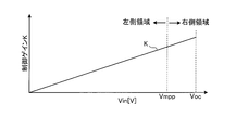
- FIG. 9 is a diagram illustrating an example of the relationship between the control gain and the supply voltage.
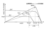
- FIG. 10 is a diagram for explaining the operation when the power supply characteristic of the power generation source suddenly changes.
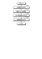
- FIG. 11 is a flowchart illustrating an example of the flow of control processing of the control unit.
- FIG. 1A is a diagram illustrating a configuration example of a power generation system according to an embodiment.
- a power generation system 100 illustrated in FIG. 1A includes a power conversion device 1 and a power generation source 2.
- the power conversion device 1 converts DC power generated by the power generation source 2 into AC power and outputs the AC power to the load 3.
- the power generation source 2 is, for example, a solar cell, a direct current generator, a fuel cell, and the like
- the load 3 is, for example, a power system or a device that operates with AC power.
- the power conversion device 1 includes a power conversion unit 10, a voltage detection unit 11, a current detection unit 12, and a control unit 20.
- the power conversion unit 10 converts the DC power supplied from the power generation source 2 into AC power based on the control by the control unit 20 and outputs the AC power to the load 3.
- the voltage detection unit 11 detects the value of the voltage supplied to the power conversion unit 10 from the power generation source 2 (hereinafter referred to as supply voltage Vin).
- the current detection unit 12 detects a value of current supplied from the power generation source 2 to the power conversion unit 10 (hereinafter referred to as supply current Iin).
- the control unit 20 controls the power conversion unit 10 by maximum power point tracking control (hereinafter referred to as MPPT control). For example, the control unit 20 controls the power conversion unit 10 so as to draw from the power generation source 2 the maximum power that can be supplied by the power generation source 2 (hereinafter referred to as the maximum supply power) based on the supply current Iin and the supply voltage Vin. To do.
- MPPT control maximum power point tracking control
- the control unit 20 includes a target command control unit 21, a feedback control unit 22, and a gain adjustment unit 23.
- the target command control unit 21 supplies a power supply voltage command Vin * (target) so that the power supplied from the power generation source 2 to the power conversion unit 10 (hereinafter referred to as supply power Pin) follows the maximum supply power of the power generation source 2. Increase or decrease (example of command).
- the feedback control unit 22 controls the power conversion unit 10 by feedback control based on a deviation between the supply voltage Vin and the power supply voltage command Vin * .
- the feedback control unit 22 controls the power conversion unit 10 so that the deviation between the supply voltage Vin and the power supply voltage command Vin * becomes zero.
- the gain adjustment unit 23 adjusts the gain of feedback control (hereinafter referred to as feedback gain) by the feedback control unit 22.
- the gain adjusting unit 23 outputs, for example, a feedback gain corresponding to the supply voltage Vin, the supply current Iin, or the power supply voltage command Vin * to the feedback control unit 22.
- the feedback control part 22 can perform feedback control by the feedback gain according to the electric power supply characteristic of the power generation source 2, for example.
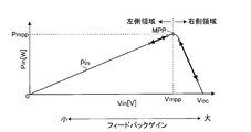
- FIG. 1B is a diagram illustrating an example of the relationship between the power supply characteristics of the power generation source 2 and the feedback control gain of the power converter 1.
- the horizontal axis indicates the supply voltage Vin
- the vertical axis indicates the supply power Pin.
- the point at which the supplied power Pin is the maximum supplied power Pmpp is called a maximum power point MPP
- the supply voltage Vin in the case of the maximum power point MPP is called a maximum power voltage Vmpp.
- the change in the supply power Pin with respect to the change in the supply voltage Vin is greater in the supply voltage Vin than in a region where the supply voltage Vin is smaller than the maximum power voltage Vmpp (hereinafter referred to as the left region).
- a region larger than the power voltage Vmpp (hereinafter referred to as a right region) is larger.
- the gain adjustment unit 23 performs target command control so that the magnitude of the feedback gain when the supply voltage Vin is in the right region is larger than the magnitude of the feedback gain when the supply voltage Vin is in the left region.
- the feedback gain of the unit 21 is adjusted.
- the arrow shown on the curve of the supplied power Pin shows an image of responsiveness.
- the maximum power point MPP can be reached quickly, while the left side region has a small feedback gain, for example, suppressing excessive response. it can.
- the power supply characteristics of the power generation source 2 are not limited to the characteristics shown in FIG. 1B, and the power converter 1 can perform feedback control with a feedback gain according to the power supply characteristics of the power generation source 2.
- the gain adjusting unit 23 provides feedback when the supply voltage Vin is in the left region. The feedback gain in the right region is made smaller than the gain.
- FIG. 2 is a diagram illustrating an example of the configuration of the power conversion device 1 illustrated in FIG. 1A.
- the power conversion device 1 includes a power conversion unit 10, voltage detection units 11, 13, and 14, current detection units 12 and 15, input terminals Tp and Tn, and output terminals T1 and T2. Is provided.
- the power conversion unit 10 includes a booster circuit 31 and an inverter circuit 32.
- the booster circuit 31 is, for example, a booster chopper circuit or a DC-DC converter
- the inverter circuit 32 is, for example, a single-phase inverter or a three-phase inverter.
- the power conversion unit 10 may include a step-down circuit that boosts the supply voltage Vin to a predetermined voltage in place of the step-up circuit 31, and the power conversion unit 10 is configured not to include the step-up circuit 31. May be.
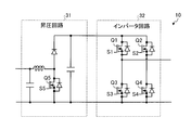
- FIG. 3 is a diagram illustrating an example of the configuration of the power conversion unit 10.
- a booster circuit 31 shown in FIG. 3 is a chopper circuit having a switching element Q5.
- the switching element Q5 is controlled to be turned on / off by the drive signal S5 output from the control unit 20, whereby the supply voltage Vin is boosted to a predetermined voltage in the booster circuit 31.
- the booster circuit 31 has, for example, an amplifier circuit that amplifies the drive signal S5 output from the control unit 20 and inputs it to the base of the switching element Q5.
- the inverter circuit 32 shown in FIG. 3 is a single-phase inverter including a plurality of bridge-connected switching elements Q1 to Q4.
- the switching elements Q1 to Q4 are controlled to be turned on / off by the drive signals S1 to S4 output from the control unit 20, whereby the inverter circuit 32 converts the DC voltage into a single-phase AC voltage.
- the inverter circuit 32 includes, for example, an amplifier circuit that amplifies the drive signals S1 to S4 output from the control unit 20 and inputs them to the bases of the switching elements Q1 to Q4.
- the voltage detector 11 detects the supply voltage Vin
- the current detector 12 detects the supply current Iin.
- the voltage detector 13 detects the value of the DC voltage after boosting output from the booster circuit 31 (hereinafter referred to as DC voltage Vpn).
- the voltage detection unit 14 detects the effective value of the AC voltage output from the power conversion unit 10 to the load 3 (hereinafter referred to as the output voltage Vout). Further, the current detection unit 15 detects an effective value (hereinafter referred to as an output current Iout) of an alternating current output from the power conversion unit 10 to the load 3.
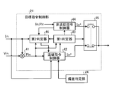
- the control unit 20 includes a target command control unit 21, a feedback control unit 22, a gain adjustment unit 23, a deviation determination unit 24, and a boost control unit 25.
- a target command control unit 21 a feedback control unit 22 a gain adjustment unit 23 a deviation determination unit 24 a boost control unit 25.
- the control unit 20 includes, for example, a microcomputer having a CPU (Central Processing Unit), a ROM (Read Only Memory), a RAM (Random Access Memory), an input / output port, and various circuits.
- the CPU of such a microcomputer reads out and executes the program stored in the ROM, thereby controlling the target command control unit 21, the feedback control unit 22, the gain adjustment unit 23, the deviation determination unit 24, and the boost control unit 25. Can be realized.
- At least one or all of the target command control unit 21, the feedback control unit 22, the gain adjustment unit 23, the deviation determination unit 24, and the step-up control unit 25 are ASIC (Application Specific Integrated Circuit), FPGA (Field Programmable Gate Array), or the like. It can also be configured with other hardware.
- ASIC Application Specific Integrated Circuit
- FPGA Field Programmable Gate Array
- Target command control unit 21 supplies power Pin increases or decreases the supply voltage command Vin * so as to follow the maximum power point MPP.
- the target command control unit 21 searches for a local maximum point other than the local maximum point searched by the process of searching for the local maximum point of the supplied power Pin (hereinafter referred to as hill-climbing process) and the hill-climbing process. (Hereinafter referred to as mountain exploration processing).
- the target command control unit 21 includes a power supply detector 41, a follow-up command controller 42 (an example of a first target command controller), a first determiner 43, and a non-follow-up command controller 44 (second target command control). An example), a switching unit 45 (an example of an output switching unit), and a second determination unit 46.
- the supply power detector 41 obtains the supply power Pin based on the supply voltage Vin and the supply current Iin. For example, the supply power detector 41 obtains the supply power Pin by multiplying the supply voltage Vin by the supply current Iin.
- Follow-up instruction control unit 42 performs hill-climbing process supply power Pin is to generate a power supply voltage command Vin * to maximize.
- the follow-up command controller 42 searches for the maximum power point MPP of the supplied power Pin by increasing / decreasing the power supply voltage command Vin * , for example, when power conversion by the power conversion unit 10 is started, and then the supplied power Pin is A power supply voltage command Vin * is generated so as to coincide with the maximum power point MPP.
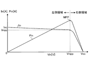
- FIG. 4 is a diagram illustrating the power supply characteristics of the power generation source 2, where the horizontal axis indicates the supply voltage Vin, and the vertical axis indicates the supply current Iin and the supply power Pin.
- the supply voltage Vin is the open voltage Voc of the power generation source 2.
- the predetermined value ⁇ V1 is set to a value smaller than a value obtained by subtracting the maximum power voltage Vmpp from the open circuit voltage Voc. Therefore, when the power supply voltage command Vin * of the initial value V0 matches the supply voltage Vin, the supply voltage Vin is a magnitude between the open voltage Voc and the maximum power voltage Vmpp, and the supply power Pin increases.
- the follow-up command controller 42 decreases the power supply voltage command Vin * by a predetermined value ⁇ V1 and outputs it to the feedback control unit 22 to decrease the supply voltage Vin by a predetermined value ⁇ V1.
- the supply voltage Vin approaches the maximum power voltage Vmpp from the open circuit voltage Voc, so that the supply power Pin approaches the maximum power point MPP.
- the follow-up command controller 42 determines that the supplied power Pin has passed through the maximum power point MPP, and increases the power supply voltage command Vin * by a predetermined value ⁇ V2 ( ⁇ V1) for feedback. Output to the control unit 22.
- the follow-up command controller 42 determines that the supply power Pin has passed the maximum power point MPP, and sets the power supply voltage command Vin * to a predetermined value ⁇ V3 ( ⁇ V2 ) And output to the feedback control unit 22.
- the follow-up command controller 42 returns the predetermined value for increasing or decreasing the power supply voltage command Vin * to the predetermined value ⁇ V1 and performs the above-described processing to maximize the supplied power Pin.
- the first determiner 43 determines whether or not the supply power Pin has reached the maximum point by increasing or decreasing the power supply voltage command Vin * by the follow-up command controller 42, and the determination result is switched to the non-follow-up command controller 44. To the determination unit 45 and the second determination unit 46.
- the first determiner 43 determines that the supplied power Pin has reached the maximum point.
- the 1st determination device 43 is, for example, when the predetermined value used for increase / decrease of the power supply voltage command Vin * by the follow-up command controller 42 is equal to or less than the threshold value or when the rate of change of the supplied power Pin is equal to or less than the threshold value It can also be determined that the supplied power Pin has reached the maximum point.
- the switching unit 45 replaces the power supply voltage command Vin * of the follow-up command controller 42 with the power supply voltage of the non-following command controller 44.
- the command Vin * is output to the feedback control unit 22.
- the switch 45 replaces the power supply voltage command Vin * of the non-following command controller 44 with the power supply voltage command of the follow-up command controller 42.
- the output of Vin * to the feedback control unit 22 is resumed.
- the non-following command controller 44 forcibly decreases the power supply voltage command Vin * by a predetermined value ⁇ Va regardless of fluctuations in the supplied power Pin.
- the power supply voltage command Vin * that decreases stepwise from the non-following command controller 44 is output to the feedback control unit 22 via the switch 45, and the supply voltage Vin decreases stepwise.
- the predetermined value ⁇ Va can be set to a value larger than the predetermined value ⁇ V1 in the hill climbing process, so that the processing speed of the mountain exploration process can be increased.
- the non-following command controller 44 ends the process of outputting the power supply voltage command Vin * , for example, when the supply voltage Vin becomes smaller than the allowable voltage Vth or when the supply power Pin becomes smaller than the allowable power Pth. . Thereby, for example, even when the control unit 20 is operated by power supplied from the power generation source 2, it is possible to avoid the control unit 20 from being stopped due to power shortage or the like.
- the second determiner 46 stores the supplied power Pin at the maximum point. Thereafter, while the power supply voltage command Vin * is output from the non-following command controller 44, the second determiner 46 determines that the supply power Pin output from the supply power detector 41 is greater than the supply power Pin at the maximum point. It is determined whether or not the value has also increased.
- the second determination unit 46 determines that there is another maximum point, and from the non-following command controller 44 The last output power supply voltage command Vin * is notified to the follow-up command controller 42.
- the second determination unit 46 determines that there is no other maximum point.
- the follow-up command controller 42 changes the value of the power supply voltage command Vin * according to the determination result by the second determiner 46. Thereby, it is possible to appropriately output the power supply voltage command Vin * according to whether or not there is another local maximum point.
- follow-up command controller 42 when it is determined by the second determiner 46 that there is no local maximum point to the other, the same value as the last power supply voltage output command Vin * (previous value) a power supply voltage command Vin * Output. Accordingly, the follow-up command controller 42 restarts the hill-climbing process, and generates the power supply voltage command Vin * so that the supplied power Pin matches the maximum power point MPP with the searched local maximum point as the maximum power point MPP. Can do.
- the follow-up command controller 42 has a power supply voltage command having the same value as the power supply voltage command Vin * last output by the non-following command controller 44. Output Vin * .
- the hill-climbing process by the following command controller 42 is started with respect to other local maximum points.
- FIG. 5 is a diagram illustrating an example of power supply characteristics of the power generation source 2 having two local maximum points.
- the power supply characteristic shown in FIG. 5 appears due to the influence of a partial shadow on the solar cell when the power generation source 2 is a solar cell, for example.
- the target command control unit 21 searches for the maximum point MP1 shown in FIG. 5 and then determines whether or not there is a supply power Pin larger than the value Pmp1 of the searched maximum point MP1 by the mountain searching process. To do.
- the target command control unit 21 performs the mountain climbing process for the other maximum point MP2.
- the target command control unit 21 can search for the maximum power point MPP and output the power supply voltage command Vin * according to the maximum power point MPP. it can. That is, even when there are two or more local maximum points in the supply power Pin of the power generation source 2 and it is difficult to search for the maximum power point MPP only by the hill climbing process, the maximum power point MPP can be searched with high accuracy. .
- the target command control unit 21 shown in FIG. 2 uses the power supply voltage command Vin * as the target command, but the target command control unit 21 can also use the power supply current command Iin * as the target command.
- FIG. 6 is a diagram illustrating an example of the target command control unit 21 that uses the power supply current command Iin * as a target command.
- the target command control unit 21 shown in FIG. 6 is obtained by replacing the voltage with a current in the target command control unit 21 shown in FIG.
- the target command control unit 21 shown in FIG. 6 replaces the power supply voltage command Vin * , the supply voltage Vin, the maximum power voltage Vmpp, the open voltage Voc, the initial value V0, the predetermined values ⁇ V1 to ⁇ V3, and the allowable voltage Vth.
- the current command Iin * supply current Iin, maximum power current Impp, open current Ioc, initial value I0, predetermined values ⁇ I1 to ⁇ I3, and allowable current Ith are used.
- the feedback control unit 22 controls the power conversion unit 10 based on the power supply voltage command Vin * output from the target command control unit 21.
- the feedback control unit 22 includes a subtracter 51, a command generation unit 52, and a drive control unit 53.
- Subtractor 51 is, for example, by subtracting the supply voltage Vin from the power supply voltage command Vin *, it obtains a difference ⁇ Vin between the power supply voltage command Vin * and supply voltage Vin.
- the command generation unit 52 is, for example, a PI controller.
- the command generation unit 52 obtains the power supply current command Iin * by performing PI (proportional integration) control on the difference ⁇ Vin.
- a control gain K (an example of a feedback gain) is set in the command generation unit 52 by the gain adjustment unit 23.
- the command generation unit 52 performs PI control on the difference ⁇ Vin with the control gain K.
- the control gain K is a proportional integral gain (proportional gain and integral gain), but only the proportional gain may be used as the control gain K, for example.
- the command generation unit 52 can perform the PI control according to the control gain K adjusted by the gain adjustment unit 23, the maximum power point followability in the MPPT control can be improved.
- the adjustment of the control gain K will be described later in detail.
- the command generation unit 52 performs a PID controller that performs PID (Proportional Integral Derivative Control), a P controller that performs P (Proportional Control) control, or PD (Proportional Derivative Control) control instead of the PI controller.
- a PD controller to perform can also be provided.
- the control gain K is set by the gain adjusting unit 23.
- the control gain K is a proportional integral derivative gain (proportional gain, integral gain and derivative gain), but only the proportional gain may be used as the control gain K, for example.
- the control gain K is a proportional gain or a differential gain. For example, only the proportional gain may be used as the control gain K.
- the drive control unit 53 generates drive signals S1 to S4 for driving the power conversion unit 10 based on the power supply current command Iin * output from the command generation unit 52.
- the drive control unit 53 includes a power command generator 54, an output current command generator 55 (an example of an output command generator), a limiter 56, and a drive signal generator 57.
- Power command generator 54 for example, by multiplying the power current command Iin * power voltage command Vin *, we obtain the source power command Pin *.
- the power command generator 54 can also obtain the power supply command Pin * in consideration of the power conversion efficiency ⁇ in the power conversion unit 10.
- the power command generator 54 can obtain the power supply power command Pin * by dividing the multiplication result of the power supply current command Iin * and the power supply voltage command Vin * by the efficiency ⁇ .
- the power command generator 54 can obtain the power supply power command Pin * by multiplying the power supply current command Iin * by the supply voltage Vin, for example, and can multiply the supply current Iin by the power supply voltage command Vin * . by, it is possible to obtain the source power command Pin *.
- the power command generator 54 can obtain the power source power command Pin * by multiplying the supply current Vin by the supply voltage Vin, for example.
- the power command generator 54 only needs to be able to determine the power supply command Pin * according to the power supply characteristics of the power generation source 2 and can also determine the power supply command Pin * by other than the above calculation.
- the power command generator 54 may obtain the power supply power command Pin * by multiplying the average value of the power supply current command Iin * and the supply current Iin by the average value of the power supply voltage command Vin * and the supply voltage Vin. it can.
- the output current command generator 55 calculates the output current command Iout * by dividing the power supply command Pin * by the output voltage Vout.
- Limiter 56 the output current command Iout * is to be equal to or less than the predetermined value, it limits the output current command Iout *.
- the drive signal generator 57 generates the drive signals S1 to S4 so that the output current Iout matches the output current command Iout *, and outputs the drive signals S1 to S4 to the inverter circuit 32.
- the output current command generator 55 only needs to control the output (for example, output power) of the power conversion unit 10 according to the power supply power command Pin *.
- the output current command generator 55 controls the output voltage Vout in addition to the output current Iout. You can also
- the feedback control unit 22 generates the power supply current command Iin * by the command generation unit 52 so that the power supply voltage command Vin * and the supply voltage Vin match, and the power supply power command is generated based on the power supply current command Iin *. Generate Pin * .
- the feedback control unit 22 Based on the power supply command Pin * , the feedback control unit 22 generates an output current command Iout * . Therefore, for example, the maximum power point followability can be improved as compared with the case where the command generator 52 generates the output current command Iout * so that the power supply voltage command Vin * and the supply voltage Vin match.
- FIG. 7 is a diagram illustrating another example of the feedback control unit in the control unit 20.
- the target command control unit 21 starts the hill climbing process
- the power supply voltage command Vin * decreases, so the supply voltage Vin becomes larger than the power supply voltage command Vin *
- the feedback control unit 22 ′ increases the output current command Iout * .
- the output power Pout increases, the supplied power Pin approaches the maximum power point MPP, and the mountain climbing process is appropriately performed.
- the feedback control unit 22 ′ increases the output current command Iout * .
- the power conversion unit 10 tries to take in more power from the power generation source 2, so the supply voltage Vin is lower than the power supply voltage command Vin * and follows the maximum power point compared to the right region. Sexuality decreases. Further, the supply voltage Vin may be excessively lower than the power supply voltage command Vin * .
- the feedback control unit 22 shown in FIG. 2 generates a power supply current command Iin * so that the power supply voltage command Vin * and the supply voltage Vin coincide with each other, and outputs the output current command Iout * based on the power supply current command Iin *. Generate.
- the supply current Iin is controlled by the power supply current command Iin *
- the supply voltage Vin is controlled by the power supply voltage command Vin * . Therefore, the change of the power supply command Pin * generated by the power supply current command Iin * and the power supply voltage command Vin * with respect to the supply voltage Vin is substantially the same as the change of the supply power Pin shown in FIG.
- the feedback control unit 22 in the left area the supply voltage Vin becomes larger than the power supply voltage command Vin *, increases the power current command Iin *.
- the power supply current command Iin * increases, the power supply power command Pin * decreases, so the output current command Iout * decreases, and thereby the output power Pout decreases.
- the feedback control unit 22 reduces the power supply current command Iin * when the supply voltage Vin becomes smaller than the power supply voltage command Vin * .
- the power supply current command Iin * decreases, the power supply power command Pin * increases, so the output current command Iout * increases, and thereby the output power Pout increases.
- the feedback control unit 22 reduces the output power Pout when the supply voltage Vin becomes larger than the power supply voltage command Vin * , and outputs when the supply voltage Vin becomes smaller than the power supply voltage command Vin *.
- the power Pout is increased. Therefore, since the feedback control unit 22 can control the output power Pout in accordance with the power supply characteristics of the power generation source 2, the supply voltage Vin can appropriately follow the power supply voltage command Vin * , and the feedback control unit 22 ' In comparison, the maximum power point followability can be improved.
- the feedback control unit 22 increases the power supply current command Iin * and increases the output power Pout. Moreover, when the supply voltage Vin becomes smaller than the power supply voltage command Vin * in the right region, the feedback control unit 22 reduces the power supply current command Iin * and reduces the output power Pout. For this reason, the feedback control unit 22 can improve the maximum power point followability similarly to the feedback control unit 22 ′.
- control unit 20 performs feedback control according to the control gain K adjusted by the gain adjustment unit 23 even when the feedback control unit 22 ′ is provided instead of the feedback control unit 22. Therefore, in the left side region, the responsiveness to the difference between the power supply voltage command Vin * and the supply voltage Vin can be reduced, an excessive decrease in the supply voltage Vin is suppressed, and the maximum power point is compared with the case where the control gain K is fixed.
- followability can be improved.
- FIG. 8 is a diagram illustrating an example of the feedback control unit 22 using the power supply current command Iin * as a target command.
- the feedback control unit 22 shown in FIG. 8 includes a subtractor 51, a command generation unit 52, and a drive control unit 53.
- the subtractor 51 obtains a difference ⁇ Iin between the power supply current command Iin * and the supply current Iin by subtracting the supply current Iin from the power supply current command Iin * , for example.
- Command generating unit 52 by performing the PI control to the difference DerutaIin, obtaining the supply voltage command Vin *.
- a control gain K is set in the command generation unit 52 by the gain adjustment unit 23.
- the command generation unit 52 performs PI control on the difference ⁇ Iin with the control gain K.
- the feedback control unit 22 illustrated in FIG. 8 may include a PID controller, a P controller, or a PD controller instead of the PI controller.
- the command generation unit 52 When the command generation unit 52 is, for example, a P controller or a PD controller, the command generation unit 52 generates a power supply power command Pin * based on the power supply voltage command Vin * , the power supply current command Iin *, and the steady deviation. be able to. Thus, even if there is a steady-state error, the source power command Pin * can be accurately generated.
- the command generation unit 52 may generate the power supply command Pin * by adding the result obtained by subtracting the steady deviation from the power supply voltage command Vin * to the power supply current command Iin *. it can.
- the command generation unit 52 may generate the power supply power command Pin * by adding the result obtained by adding the steady deviation to the power supply voltage command Vin * to the power supply current command Iin *. it can.
- the drive control unit 53 has the same configuration as the drive control unit 53 shown in FIG. 2, and generates drive signals S1 to S4 for driving the power conversion unit 10 based on the power supply voltage command Vin * output from the command generation unit 52. Generate.
- the command generation unit 52 shown in FIG. 8 also has the PI control, PID control, P control, or PD according to the control gain K adjusted by the gain adjustment unit 23, similarly to the command generation unit 52 shown in FIG. Since the control is performed, the maximum power point followability in the MPPT control can be improved.
- the feedback control unit 22 shown in FIG. 8 generates the power supply voltage command Vin * by the command generation unit 52 so that the power supply current command Iin * and the supply current Iin match, and the power supply voltage command Vin * is based on the power supply voltage command Vin *.
- a power command Pin * is generated.
- the feedback control unit 22 Based on the power supply command Pin * , the feedback control unit 22 generates an output current command Iout * . Therefore, the maximum power point followability can be improved as compared with the case where the output current command Iout * is output from the command generation unit 52 (see FIG. 7).
- the gain adjusting unit 23 has a table or an arithmetic expression that associates the control gain K with the supply voltage Vin or the supply current Iin, and adjusts the control gain K according to the supply voltage Vin or the supply current Iin.
- the gain adjusting unit 23 can obtain the control gain K corresponding to the supply voltage Vin based on the following arithmetic expression (1).
- the gain adjustment unit 23 sets the obtained control gain K in the command generation unit 52 of the feedback control unit 22.
- K1 is a coefficient and is set to a predetermined value.
- K K1 ⁇ Vin (1)
- FIG. 9 is a diagram illustrating an example of the relationship between the control gain K and the supply voltage Vin.
- the calculation result of the above equation (1) for Vin (for example, from the predetermined value Vmin to the rated input voltage Vmax) can be stored in the gain adjustment unit 23 as a table.
- the gain adjusting unit 23 acquires the control gain K corresponding to the supply voltage Vin from the stored table, and sets the control gain K in the command generation unit 52 of the feedback control unit 22.
- the gain adjusting unit 23 can increase the control gain K in the right region rather than the left region. Therefore, the power conversion device 1 can improve the maximum power point followability in the MPPT control, and can suppress the supply voltage Vin from excessively decreasing even when the supply voltage Vin is in the left region.
- the supply current Iin has a larger change in the supply current Iin relative to the change in the supply voltage Vin in the right region than in the left region. Therefore, by increasing the control gain K in the right region relative to the control gain K in the left region, the followability of the supply current Iin with respect to the power supply current command Iin * can be improved in the right region. Thereby, for example, the time until the supplied power Pin reaches the maximum power point MPP in the hill climbing process can be shortened.
- the feedback control unit 22 increases the output current command Iout * when the supply voltage Vin becomes smaller than the power supply voltage command Vin * in the right region. Therefore, when the control gain K is increased as in the left region, the response of increasing the output current command Iout * is increased, and the degree to which the supply voltage Vin decreases is increased. When the difference between the supply voltage Vin and the power supply voltage command Vin * is large, the supply voltage Vin may be excessively reduced.
- the gain adjusting unit 23 makes the control gain K in the left region smaller than the control gain K in the right region, even if the supply voltage Vin is smaller than the power supply voltage command Vin * in the left region, the supply is performed. It is possible to suppress the voltage Vin from excessively decreasing.
- the gain adjusting unit 23 increases the control gain K as the supply voltage Vin increases. Therefore, even when the maximum power voltage Vmpp (see FIG. 4) changes, the control gain K in the right region can be made larger than the left region.
- the gain adjusting unit 23 can further adjust the control gain K according to the amount of sunshine to the solar voltage. For example, the gain adjusting unit 23 increases the control gain K as the amount of sunshine increases.
- the control unit 20 In a state where the control unit 20 is not controlling the power conversion unit 10, the supply voltage Vin is the open circuit voltage Voc.
- the open circuit voltage Voc increases as the amount of sunshine to the solar voltage increases. Therefore, the control unit 20 sets a control gain K corresponding to the open circuit voltage Voc when starting control of the power conversion unit 10.
- the gain adjustment unit 23 obtains the control gain K corresponding to the supply voltage Vin based on the following calculation formula (2), for example.
- the gain adjustment unit 23 sets the obtained control gain K in the command generation unit 52 of the feedback control unit 22.
- the power converter 10 can further shorten the time until the supplied power Pin reaches the maximum power point MPP in the hill climbing process, for example, and can further increase the maximum power point followability. it can.
- the gain adjustment unit 23 adjusts the control gain K based on the magnitude of the maximum supply power Pmpp after the supply power Pin reaches the maximum power point MPP.
- the gain adjusting unit 23 can obtain the control gain K corresponding to the supply voltage Vin based on, for example, the following arithmetic expression (3).
- the gain adjustment unit 23 sets the obtained control gain K in the command generation unit 52 of the feedback control unit 22.
- K K1 ⁇ Vin ⁇ f (Pmpp) (3)
- f (Pmpp) is an arithmetic expression for an adjustment coefficient corresponding to the maximum power supply Pmpp, and is expressed by, for example, the following arithmetic expression (4).
- f (Pmpp) K2 ⁇ Pmpp (4)
- the gain adjusting unit 23 may include a detection unit that directly detects the amount of sunlight instead of the open circuit voltage Voc and the maximum supply power Pmpp, and may adjust the control gain K based on the detection result by the detection unit.
- the gain adjustment unit 23 acquires a control gain K corresponding to the supply current Iin by a table or an arithmetic expression relating the supply current Iin and the control gain K, and sets the control gain K in the feedback control unit 22. You can also. For example, the gain adjusting unit 23 obtains the control gain K corresponding to the supply current Iin based on the arithmetic expression in which “Vin” is replaced with “1 / Iin” in the arithmetic expressions (1) to (3). it can.
- the gain adjustment unit 23 replaces the calculation of the control gain K with the arithmetic expressions (1) to (3), or the relationship between the supply voltage Vin and the maximum power voltage Vmpp (see FIG. 4) or the supply current Iin and the maximum power.
- the control gain K can also be adjusted based on the relationship with the current Impp (see FIG. 4). This also makes it possible to make the control gain K in the right region higher than the control gain K in the left region.
- the gain adjusting unit 23 sets the control gain K to a predetermined value until the supply voltage Vin or the supply current Iin reaches the maximum power voltage Vmpp or the maximum power current Impp after the target command control unit 21 starts the hill climbing process. Set to k1. Further, after the supply voltage Vin or the supply current Iin reaches the maximum power voltage Vmpp or the maximum power current Impp, the gain adjustment unit 23 sets the control gain K to a predetermined value k2 ( ⁇ k1).
- the gain adjusting unit 23 can change the control gain K before and after the supply voltage Vin or the supply current Iin reaches the maximum power voltage Vmpp or the maximum power current Imppp corresponding to the maximum supply power Pmpp. it can. Therefore, for example, it is possible to shorten the time until the supplied power Pin reaches the maximum power point MPP in the hill-climbing process, and it is possible to improve the maximum power point followability.
- the gain adjustment unit 23 stores, for example, information indicating the relationship between the open circuit voltage Voc and the maximum power voltage Vmpp, and when starting control of the power conversion unit 10, the maximum power voltage Vmpp is determined according to the open circuit voltage Voc. Can also be determined. In this case, the gain adjusting unit 23 sets the control gain K to the predetermined value k1 when the supply voltage Vin is higher than the maximum power voltage Vmpp, and sets the control gain K to the predetermined value k2 (when the supply voltage Vin is less than the maximum power voltage Vmpp). ⁇ K1).
- the gain adjusting unit 23 can also obtain the control gain K according to the supply voltage Vin and the supply current Iin. For example, the gain adjusting unit 23 can set the average value of the control gain corresponding to the supply voltage Vin and the control gain corresponding to the supply current Iin as the control gain K.
- the gain adjusting unit 23 can also adjust the control gain K according to the power supply voltage command Vin * .
- the control gain K corresponding to the power supply voltage command Vin * can be performed by replacing “Vin * ” with “Vin * ” described above.
- the gain adjusting unit 23 can obtain the control gain K corresponding to the power supply voltage command Vin * based on the arithmetic expression shown in the following expression (5).
- K K1 ⁇ Vin * (5)
- the gain adjusting unit 23 can also obtain a control gain K corresponding to the power supply current command Iin * and set the obtained control gain K in the command generating unit 52 of the feedback control unit 22.
- the control gain K corresponding to the power supply current command Iin * can be performed by replacing “Iin” with “Iin * ”.
- the deviation determination unit 24 determines whether or not the supply voltage Vin is larger than the power supply voltage command Vin * by a predetermined value Vlim and notifies the follow-up command controller 42 of the determination result.
- FIG. 10 is a diagram for explaining the operation when the power supply characteristic of the power generation source 2 changes suddenly. As shown in FIG. 10, it is assumed that the power supply characteristic of the power generation source 2 suddenly changes from Pin1 to Pin2, and the maximum power point changes from MPP1 to MPP2. For example, when the power generation source 2 is a solar cell, the maximum power point changes as shown in FIG. 10 when the amount of sunshine on the solar cell is suddenly changed from a low state to a high state.
- the supply current Iin is the maximum power current Impp1. Since the output current command Iout * does not change at the moment when the power supply characteristic of the power generation source 2 suddenly changes from Pin1 to Pin2, the supply current Iin is the maximum power current Impp1. Therefore, the supply voltage Vin changes to the voltage Vb.
- the difference between the power supply voltage command Vin * and the supply voltage Vin is a value ⁇ Vb obtained by subtracting the maximum power voltage Vmpp1 from the voltage Vb.
- the deviation determination unit 24 determines whether or not the value ⁇ Vb is equal to or greater than a predetermined value Vlim.
- the follow-up command controller 42 sets the voltage Vb to the power supply voltage command Vin * . Since the power supply voltage command Vin * matches the voltage Vb, the output of the subtractor 51 becomes zero, and after the output fluctuation of the command generator 52 stops instantaneously, the hill climbing process is started from the right region.
- the control unit 20 starts the hill climbing process by the target command control unit 21 from the right region, and thus increases the maximum power point tracking performance. In addition, it is possible to suppress excessive power from being instantaneously drawn from the power generation source 2.
- the feedback control unit 22 When the feedback control unit 22 has the configuration shown in FIG. 8, it is determined whether or not the supply current Iin is larger than the power supply current command Iin * by a predetermined value Ilim or not.
- the deviation determination unit 24 notifies the follow-up command controller 42 of whether or not the supply current Iin is greater than or equal to the predetermined value Ilim than the power supply current command Iin * .
- the boost control unit 25 generates the drive signal S5 and outputs the drive signal S5 to the booster circuit 31 so that the DC voltage Vpn that is the boosted voltage by the booster circuit 31 becomes a predetermined value.
- the drive signal S5 is, for example, a PWM signal.
- FIG. 11 is a flowchart illustrating an example of the flow of control processing of the control unit 20.
- the control unit 20 repeatedly executes the control process shown in FIG. 11 at a predetermined cycle. For example, when the power conversion by the power conversion unit 10 is started, the control unit 20 starts the control process illustrated in FIG.
- the control unit 20 generates a target command in, for example, the above-described hill-climbing process and hill-searching process (step S10).
- the target command is the power supply voltage command Vin * or the power supply current command Iin * .
- the control unit 20 generates a new power supply voltage when the supply voltage Vin matches the power supply voltage command Vin * generated in the mountain climbing process or the mountain exploration process, or when the power supply voltage command Vin * is generated and a predetermined time elapses.
- a command Vin * is generated. For example, when the supply voltage Vin is higher than the power supply voltage command Vin * by a predetermined value or more, the control unit 20 sets the supply voltage Vin to the power supply voltage command Vin * .
- control unit 20 adjusts the control gain K (step S11).
- control unit 20 obtains a control gain K corresponding to the supply voltage Vin or the supply current Iin, for example, and sets the control gain K in the feedback control unit 22.
- the control unit 20 generates an output current command Iout * based on the control gain K adjusted in step S11 (step S12). For example, the control unit 20 obtains the power supply current command Iin * by PI control using the control gain K adjusted in step S11, and generates the output current command Iout * based on the power supply current command Iin * .
- control unit 20 generates drive signals S1 to S4 for driving the power conversion unit 10 based on the power supply current command Iin * output from the command generation unit 52 (step S13).
- the power conversion device 1 can improve the maximum power point followability by adjusting the control gain K according to the supply voltage Vin or the supply current Iin.
- the power conversion unit 10 of the above-described embodiment converts DC power into AC power, but the power conversion unit 10 converts DC power of the power generation source 2 into DC power of a predetermined voltage. May be.
- the power conversion unit 10 has a configuration that does not include the inverter circuit 32, and the power conversion device 1 includes a voltage detection unit that detects the value of the output current of the booster circuit 31. Then, the control unit 20 generates the drive signal S5 based on the output current of the booster circuit 31 and the output current command Iout * .
- the feedback control unit 22 has the function of the boost control unit 25.
- FIGS. 2 and 6 to 8 indicate the direction of the flow of information (for example, data and signals) and control in an auxiliary manner. It is not meant to be a limitation.
Landscapes
- Engineering & Computer Science (AREA)
- Power Engineering (AREA)
- General Physics & Mathematics (AREA)
- Physics & Mathematics (AREA)
- Radar, Positioning & Navigation (AREA)
- Automation & Control Theory (AREA)
- Electromagnetism (AREA)
- Life Sciences & Earth Sciences (AREA)
- Sustainable Development (AREA)
- Sustainable Energy (AREA)
- Dc-Dc Converters (AREA)
- Supply And Distribution Of Alternating Current (AREA)
- Control Of Electrical Variables (AREA)
Abstract
実施形態に係る電力変換装置は、目標指令制御部と、フィードバック制御部と、ゲイン調整部とを備える。目標指令制御部は、発電源から電力変換部への供給電力が発電源の最大供給電力に追従するように目標指令を増減する。フィードバック制御部は、発電源から電力変換部への供給電圧および供給電流の少なくとも一方と目標指令との偏差に基づくフィードバック制御によって電力変換部を制御する。ゲイン調整部は、前記供給電圧、前記供給電流および前記目標指令のうちの少なくとも一つに基づいて前記フィードバック制御部のゲインを調整する。
Description
開示の実施形態は、電力変換装置、発電システム、制御装置および制御方法に関する。
従来、発電システムにおいて、太陽電池などの発電源から供給される電力を所定の電力へ変換する電力変換装置が知られている。かかる電力変換装置は、一般に、最大電力点追従制御と呼ばれる機能を有しており、発電源から電力変換部へ供給される電流および電圧に基づき、発電源の出力電力が最大になるように電力変換部を制御する(例えば、特許文献1参照)。
上述した電力変換装置においては、最大電力点追従制御における最大電力点追従性を高めることが望まれる。
実施形態の一態様は、上記に鑑みてなされたものであって、最大電力点追従制御における最大電力点追従性を高めることができる電力変換装置、発電システム、制御装置および制御方法を提供することを目的とする。
実施形態の一態様に係る電力変換装置は、電力変換部と、目標指令制御部と、フィードバック制御部と、ゲイン調整部とを備える。前記電力変換部は、発電源の電力を所定の電力へ変換する。前記目標指令制御部は、前記発電源から前記電力変換部への供給電力が前記発電源の最大供給電力に追従するように目標指令を増減する。前記フィードバック制御部は、前記発電源から前記電力変換部への供給電圧および供給電流の少なくとも一方と前記目標指令との偏差に基づくフィードバック制御によって前記電力変換部を制御する。前記ゲイン調整部は、前記供給電圧、前記供給電流および前記目標指令のうちの少なくとも一つに基づいて前記フィードバック制御のゲインを調整する。
実施形態の一態様によれば、最大電力点追従制御における最大電力点追従性を高めることができる電力変換装置、発電システム、制御装置および制御方法を提供することができる。
以下、添付図面を参照して、本願の開示する電力変換装置、発電システム、制御装置および制御方法の実施形態を詳細に説明する。なお、以下に示す実施形態によりこの発明が限定されるものではない。
[1.発電システム]
図1Aは、実施形態に係る発電システムの構成例を示す図である。図1Aに示す発電システム100は、電力変換装置1および発電源2を備える。電力変換装置1は、発電源2で発電された直流電力を交流電力へ変換して負荷3へ出力する。なお、発電源2は、例えば、太陽電池、直流発電機、燃料電池などであり、負荷3は、例えば、電力系統、交流電力で動作する機器である。
図1Aは、実施形態に係る発電システムの構成例を示す図である。図1Aに示す発電システム100は、電力変換装置1および発電源2を備える。電力変換装置1は、発電源2で発電された直流電力を交流電力へ変換して負荷3へ出力する。なお、発電源2は、例えば、太陽電池、直流発電機、燃料電池などであり、負荷3は、例えば、電力系統、交流電力で動作する機器である。
電力変換装置1は、電力変換部10と、電圧検出部11と、電流検出部12と、制御部20とを備える。電力変換部10は、制御部20による制御に基づき、発電源2から供給される直流電力を交流電力へ変換して負荷3へ出力する。
電圧検出部11は、発電源2から電力変換部10へ供給される電圧の値(以下、供給電圧Vinと記載する)を検出する。また、電流検出部12は、発電源2から電力変換部10へ供給される電流の値(以下、供給電流Iinと記載する)を検出する。
制御部20は、最大電力点追従制御(以下、MPPT制御と記載する)により電力変換部10を制御する。例えば、制御部20は、供給電流Iinおよび供給電圧Vinに基づき、発電源2が供給できる最大の電力(以下、最大供給電力と記載する)を発電源2から引き出すように電力変換部10を制御する。
かかる制御部20は、目標指令制御部21と、フィードバック制御部22と、ゲイン調整部23とを備える。目標指令制御部21は、発電源2から電力変換部10へ供給される電力(以下、供給電力Pinと記載する)が発電源2の最大供給電力に追従するように電源電圧指令Vin*(目標指令の一例)を増減する。
フィードバック制御部22は、供給電圧Vinと電源電圧指令Vin*との偏差に基づくフィードバック制御によって電力変換部10を制御する。フィードバック制御部22は、例えば、供給電圧Vinと電源電圧指令Vin*との偏差がゼロになるように、電力変換部10を制御する。
ゲイン調整部23は、フィードバック制御部22によるフィードバック制御のゲイン(以下、フィードバックゲインと記載する)を調整する。ゲイン調整部23は、例えば、供給電圧Vin、供給電流Iinまたは電源電圧指令Vin*に応じたフィードバックゲインをフィードバック制御部22に出力する。これにより、フィードバック制御部22は、例えば、発電源2の電力供給特性に応じたフィードバックゲインによってフィードバック制御を行うことができる。
図1Bは、発電源2の電力供給特性と電力変換装置1のフィードバック制御のゲインとの関係例を示す図であり、横軸は供給電圧Vinを示し、縦軸は、供給電力Pinを示す。また、供給電力Pinが最大供給電力Pmppである点を最大電力点MPPと呼び、最大電力点MPPの場合の供給電圧Vinを最大電力電圧Vmppと呼ぶ。
図1Bに示す特性例において、供給電圧Vinの変化に対する供給電力Pinの変化は、供給電圧Vinが最大電力電圧Vmppよりも小さい領域(以下、左側領域と記載する)よりも、供給電圧Vinが最大電力電圧Vmppよりも大きい領域(以下、右側領域と記載する)の方が大きい。
そこで、ゲイン調整部23は、例えば、供給電圧Vinが右側領域にある場合のフィードバックゲインの大きさが、供給電圧Vinが左側領域にある場合のフィードバックゲインの大きさよりも大きくなるように目標指令制御部21のフィードバックゲインを調整する。図1Bにおいて、供給電力Pinの曲線上に示される矢印は、応答性のイメージを示す。
このようにフィードバックゲインを調整することにより、最大電力電圧Vmppよりも供給電圧Vinが大きい右側領域のように、供給電圧Vinの変化に対する供給電力Pinの変化が大きい領域において、MPPT制御の応答性、すなわち、最大電力点追従制御性を高めることができる。
また、例えば、発電源2の開放電圧VocからMPPT制御を行う場合に、最大電力点MPPへ早く到達させることができ、一方、左側領域では、フィードバックゲインが小さいため、例えば、過度な応答を抑制できる。
なお、発電源2の電力供給特性は、図1Bに示す特性に限られるものではなく、電力変換装置1は、発電源2の電力供給特性に応じたフィードバックゲインでフィードバック制御を行うことができる。例えば、供給電圧Vinの変化に対する供給電力Pinの変化が左側領域よりも右側領域の方が小さい特性を有する発電源2に対して、ゲイン調整部23は、供給電圧Vinが左側領域の場合のフィードバックゲインよりも右側領域の場合のフィードバックゲインの大きさを小さくする。
以下、図1Aに示す電力変換装置1の構成例についてさらに詳細に説明する。
[2.電力変換装置]
図2は、図1Aに示す電力変換装置1の構成の一例を示す図である。図2に示すように、電力変換装置1は、電力変換部10と、電圧検出部11、13、14と、電流検出部12、15と、入力端子Tp、Tnと、出力端子T1、T2とを備える。
図2は、図1Aに示す電力変換装置1の構成の一例を示す図である。図2に示すように、電力変換装置1は、電力変換部10と、電圧検出部11、13、14と、電流検出部12、15と、入力端子Tp、Tnと、出力端子T1、T2とを備える。
電力変換部10は、昇圧回路31と、インバータ回路32とを備える。昇圧回路31は、例えば、昇圧チョッパ回路やDC-DCコンバータであり、また、インバータ回路32は、例えば、単相インバータや3相インバータである。なお、電力変換部10は、昇圧回路31に代えて、供給電圧Vinを所定の電圧に昇圧する降圧回路を備えることもでき、また、電力変換部10は、昇圧回路31を設けない構成であってもよい。
図3は、電力変換部10の構成の一例を示す図である。図3に示す昇圧回路31は、スイッチング素子Q5を有するチョッパ回路である。かかるスイッチング素子Q5は、制御部20から出力される駆動信号S5によってON/OFFが制御され、これにより、昇圧回路31において供給電圧Vinが所定の電圧に昇圧される。なお、図示しないが昇圧回路31は、例えば、制御部20から出力される駆動信号S5を増幅してスイッチング素子Q5のベースへ入力する増幅回路を有する。
また、図3に示すインバータ回路32は、ブリッジ接続された複数のスイッチング素子Q1~Q4を含む単相インバータである。かかるスイッチング素子Q1~Q4は、制御部20から出力される駆動信号S1~S4によりON/OFFが制御され、これにより、インバータ回路32において、直流電圧が単相交流電圧へ変換される。なお、図示しないがインバータ回路32は、例えば、制御部20から出力される駆動信号S1~S4を増幅してスイッチング素子Q1~Q4のベースへ入力する増幅回路を有する。
図2に戻って電力変換装置1の説明を続ける。電圧検出部11は、供給電圧Vinを検出し、電流検出部12は、供給電流Iinを検出する。また、電圧検出部13は、昇圧回路31から出力される昇圧後の直流電圧の値(以下、直流電圧Vpnと記載する)を検出する。
電圧検出部14は、電力変換部10から負荷3へ出力される交流電圧の実効値(以下、出力電圧Voutと記載する)を検出する。また、電流検出部15は、電力変換部10から負荷3へ出力される交流電流の実効値(以下、出力電流Ioutと記載する)を検出する。
制御部20は、目標指令制御部21と、フィードバック制御部22と、ゲイン調整部23と、偏差判定部24と、昇圧制御部25とを備える。以下、制御部20の構成について詳細に説明する。
なお、制御部20は、例えば、CPU(Central Processing Unit)、ROM(Read Only Memory)、RAM(Random Access Memory)、入出力ポートなどを有するマイクロコンピュータや各種の回路を含む。かかるマイクロコンピュータのCPUは、ROMに記憶されているプログラムを読み出して実行することにより、目標指令制御部21、フィードバック制御部22、ゲイン調整部23、偏差判定部24および昇圧制御部25の制御を実現することができる。
また、目標指令制御部21、フィードバック制御部22、ゲイン調整部23、偏差判定部24および昇圧制御部25の少なくともいずれかまたは全部をASIC(Application Specific Integrated Circuit)やFPGA(Field Programmable Gate Array)等のハードウェアで構成することもできる。
[2.1.目標指令制御部21]
目標指令制御部21は、供給電力Pinが最大電力点MPPに追従するように電源電圧指令Vin*を増減する。例えば、目標指令制御部21は、供給電力Pinの極大点を探索する処理(以下、山登り処理と記載する)と、山登り処理で探索された極大点の他に極大点がないかを探索する処理(以下、山探り処理と記載する)とを行う。
目標指令制御部21は、供給電力Pinが最大電力点MPPに追従するように電源電圧指令Vin*を増減する。例えば、目標指令制御部21は、供給電力Pinの極大点を探索する処理(以下、山登り処理と記載する)と、山登り処理で探索された極大点の他に極大点がないかを探索する処理(以下、山探り処理と記載する)とを行う。
目標指令制御部21は、供給電力検出器41と、追従指令制御器42(第1目標指令制御器の一例)と、第1判定器43と、非追従指令制御器44(第2目標指令制御器の一例)と、切替器45(出力切替器の一例)と、第2判定器46とを備える。
供給電力検出器41は、供給電圧Vinと供給電流Iinとに基づき、供給電力Pinを求める。例えば、供給電力検出器41は、供給電圧Vinに供給電流Iinを乗算することにより、供給電力Pinを求める。
追従指令制御器42は、供給電力Pinが最大化するように電源電圧指令Vin*を生成して山登り処理を行う。追従指令制御器42は、例えば、電力変換部10による電力変換が開始される際に、電源電圧指令Vin*を増減して供給電力Pinの最大電力点MPPを探索し、その後、供給電力Pinが最大電力点MPPと一致するように、電源電圧指令Vin*を生成する。
ここで、追従指令制御器42における山登り処理の一例を説明する。図4は、発電源2の電力供給特性を示す図であり、横軸は供給電圧Vinを示し、縦軸は、供給電流Iinおよび供給電力Pinを示す。
追従指令制御器42は、山登り処理において、例えば、供給電圧Vinから所定値ΔV1を減算した値を、電源電圧指令Vin*の初期値V0(=Vin-ΔV1)として設定し、フィードバック制御部22へ出力する。なお、山登り処理の開始時点では、電力変換部10による電力変換が開始されていないため、供給電圧Vinは、発電源2の開放電圧Vocである。
所定値ΔV1は、開放電圧Vocから最大電力電圧Vmppを減算した値よりも小さい値に設定される。そのため、初期値V0の電源電圧指令Vin*と供給電圧Vinが一致した場合に、供給電圧Vinは開放電圧Vocと最大電力電圧Vmppとの間の大きさであり、供給電力Pinは増加する。
追従指令制御器42は、供給電力Pinの増加が継続する限り、電源電圧指令Vin*を所定値ΔV1ずつ減少させてフィードバック制御部22へ出力し、供給電圧Vinを所定値ΔV1ずつ減少させる。これにより、供給電圧Vinが開放電圧Vocから最大電力電圧Vmppへ近づくため、供給電力Pinが最大電力点MPPに近づいていく。
そして、供給電力Pinが減少した場合、追従指令制御器42は、供給電力Pinが最大電力点MPPを通過したと判定し、電源電圧指令Vin*を所定値ΔV2(<ΔV1)だけ増加させてフィードバック制御部22へ出力する。かかる電源電圧指令Vin*により、供給電力Pinが増加した場合、追従指令制御器42は、供給電力Pinが最大電力点MPPを通過したと判定し、電源電圧指令Vin*を所定値ΔV3(<ΔV2)だけ減少させてフィードバック制御部22へ出力する。
以降、追従指令制御器42は、例えば、最大電力点MPPの通過の判定と電源電圧指令Vin*を増減させる所定値の減少を繰り返すことにより、供給電力Pinを最大電力点MPPに追従させる。なお、追従指令制御器42は、最大電力点MPPが変動した場合、例えば、電源電圧指令Vin*を増減させる所定値を所定値ΔV1に戻して上述した処理を行うことで、供給電力Pinを最大電力点MPPに追従させる。
図2に戻って目標指令制御部21の説明を続ける。第1判定器43は、追従指令制御器42による電源電圧指令Vin*の増減により供給電力Pinが極大点に到達したか否かを判定し、かかる判定結果を、非追従指令制御器44、切替器45および第2判定器46に通知する。
第1判定器43は、例えば、供給電力Pinが最大電力点MPPを通過したことを示す情報を追従指令制御器42から取得した場合に、供給電力Pinが極大点に到達したと判定する。なお、第1判定器43は、例えば、追従指令制御器42で電源電圧指令Vin*の増減に用いられる所定値が閾値以下になった場合や供給電力Pinの変化率が閾値以下になった場合に供給電力Pinが極大点に到達したと判定することもできる。
切替器45は、第1判定器43によって供給電力Pinが極大点に到達したと判定された場合、追従指令制御器42の電源電圧指令Vin*に代えて、非追従指令制御器44の電源電圧指令Vin*をフィードバック制御部22へ出力する。
切替器45は、非追従指令制御器44からの電源電圧指令Vin*の出力処理が終了すると、非追従指令制御器44の電源電圧指令Vin*に代えて、追従指令制御器42の電源電圧指令Vin*のフィードバック制御部22への出力を再開する。
非追従指令制御器44は、例えば、供給電力Pinの変動に関わらず、電源電圧指令Vin*を強制的に所定値ΔVaずつ繰り返し減少させる。これにより、非追従指令制御器44からステップ状に減少する電源電圧指令Vin*が切替器45を介してフィードバック制御部22へ出力され、供給電圧Vinが段階的に減少する。なお、所定値ΔVaは、山登り処理における所定値ΔV1よりも大きな値に設定することで、山探り処理の処理速度を高めることができる。
非追従指令制御器44は、例えば、供給電圧Vinが許容電圧Vthより小さくなった場合、または、供給電力Pinが許容電力Pthより小さくなった場合、電源電圧指令Vin*を出力する処理を終了する。これにより、例えば、発電源2から供給される電力により制御部20が動作する場合でも、制御部20が電力不足等で停止することを回避できる。
第2判定器46は、第1判定器43によって供給電力Pinが極大点に到達したと判定された場合、かかる極大点における供給電力Pinを記憶する。その後、第2判定器46は、非追従指令制御器44から、電源電圧指令Vin*が出力されている間に、供給電力検出器41から出力される供給電力Pinが極大点における供給電力Pinよりも大きくなったか否かを判定する。
第2判定器46は、供給電力検出器41から出力される供給電力Pinが極大点における供給電力Pinよりも大きくなった場合、他に極大点があると判定し、非追従指令制御器44から最後に出力された電源電圧指令Vin*の値を追従指令制御器42へ通知する。一方、供給電力検出器41から出力される供給電力Pinが極大点における供給電力Pinよりも大きくならない場合、第2判定器46は、他に極大点がないと判定する。
追従指令制御器42は、第2判定器46による判定結果に応じて、電源電圧指令Vin*の値を変える。これにより、他に極大点があるか否かに応じて適切に電源電圧指令Vin*を出力することができる。
例えば、追従指令制御器42は、第2判定器46により他に極大点がないと判定された場合、最後に出力した電源電圧指令Vin*(前回値)と同じ値の電源電圧指令Vin*を出力する。これにより、追従指令制御器42は、山登り処理を再開し、探索済みの極大点を最大電力点MPPとして供給電力Pinが最大電力点MPPと一致するように、電源電圧指令Vin*を生成することができる。
一方、追従指令制御器42は、第2判定器46により他に極大点があると判定された場合、非追従指令制御器44が最後に出力した電源電圧指令Vin*と同じ値の電源電圧指令Vin*を出力する。これにより、他の極大点に対して追従指令制御器42による山登り処理が開始される。
例えば、発電源2の電力供給特性が図5に示す状態であるとする。図5は、2つの極大点を有する発電源2の電力供給特性の一例を示す図である。図5に示す電力供給特性は、例えば、発電源2が太陽電池である場合に、太陽電池への部分影の影響によって現れる。
目標指令制御部21は、山登り処理において、図5に示す極大点MP1を探索した後、山探り処理により、探索済みの極大点MP1の値Pmp1よりも大きな供給電力Pinがあるか否かを判定する。図5に示す例では、山探り処理によって極大点MP1の値Pmp1よりも大きな供給電力Pinの値P1が発見されるため、目標指令制御部21は、他の極大点MP2に対する山登り処理を行う。
これにより、目標指令制御部21は、極大点が2つ以上であったとしても、最大電力点MPPを探索することができ、最大電力点MPPに応じた電源電圧指令Vin*を出力することができる。すなわち、発電源2の供給電力Pinに極大点が2つ以上あり、山登り処理だけで最大電力点MPPを探索することが難しい場合であっても、精度よく最大電力点MPPを探索することができる。
なお、図2に示す目標指令制御部21は、電源電圧指令Vin*を目標指令としたが、目標指令制御部21は、電源電流指令Iin*を目標指令とすることもできる。図6は、電源電流指令Iin*を目標指令とする目標指令制御部21の一例を示す図である。
図6に示す目標指令制御部21は、図2に示す目標指令制御部21において電圧を電流に置き換えたものである。例えば、図6に示す目標指令制御部21は、電源電圧指令Vin*、供給電圧Vin、最大電力電圧Vmpp、開放電圧Voc、初期値V0、所定値ΔV1~ΔV3、許容電圧Vthに代えて、電源電流指令Iin*、供給電流Iin、最大電力電流Impp、開放電流Ioc、初期値I0、所定値ΔI1~ΔI3、許容電流Ithを用いる。
[2.2.フィードバック制御部22]
次に、図2に示すフィードバック制御部22について説明する。フィードバック制御部22は、目標指令制御部21から出力される電源電圧指令Vin*に基づいて電力変換部10を制御する。かかるフィードバック制御部22は、図2に示すように、減算器51と、指令生成部52と、駆動制御部53とを備える。
次に、図2に示すフィードバック制御部22について説明する。フィードバック制御部22は、目標指令制御部21から出力される電源電圧指令Vin*に基づいて電力変換部10を制御する。かかるフィードバック制御部22は、図2に示すように、減算器51と、指令生成部52と、駆動制御部53とを備える。
減算器51は、例えば、電源電圧指令Vin*から供給電圧Vinを減算することにより、電源電圧指令Vin*と供給電圧Vinとの差分ΔVinを求める。
指令生成部52は、例えば、PI制御器である。かかる指令生成部52は、差分ΔVinに対しPI(比例積分)制御を行うことにより、電源電流指令Iin*を求める。指令生成部52には、ゲイン調整部23により制御ゲインK(フィードバックゲインの一例)が設定される。指令生成部52は、かかる制御ゲインKにより差分ΔVinに対しPI制御を行う。なお、制御ゲインKは、比例積分ゲイン(比例ゲインおよび積分ゲイン)であるが、例えば、比例ゲインのみを制御ゲインKとしてもよい。
指令生成部52は、ゲイン調整部23によって調整された制御ゲインKに応じたPI制御を行うことができるため、MPPT制御における最大電力点追従性を高めることができる。かかる制御ゲインKの調整については後で詳述する。
なお、指令生成部52は、PI制御器に代えて、PID(Proportional Integral Derivative Control)を行うPID制御器、P(Proportional Control)制御を行うP制御器、または、PD(Proportional Derivative Control)制御を行うPD制御器を設けることもできる。この場合も同様に、ゲイン調整部23により制御ゲインKが設定される。なお、PID制御器の場合、制御ゲインKは、比例積分微分ゲイン(比例ゲイン、積分ゲインおよび微分ゲイン)であるが、例えば、比例ゲインのみを制御ゲインKとしてもよい。また、PD制御器の場合、制御ゲインKは、比例ゲイン、微分ゲインであるが、例えば、比例ゲインのみを制御ゲインKとしてもよい。
駆動制御部53は、指令生成部52から出力される電源電流指令Iin*に基づいて電力変換部10を駆動する駆動信号S1~S4を生成する。かかる駆動制御部53は、電力指令生成器54と、出力電流指令生成器55(出力指令生成器の一例)と、リミッタ56と、駆動信号生成器57とを備える。
電力指令生成器54は、例えば、電源電流指令Iin*に電源電圧指令Vin*を乗算することによって、電源電力指令Pin*を求める。なお、電力指令生成器54は、電力変換部10における電力変換の効率ζを考慮して、電源電力指令Pin*を求めることもできる。例えば、電力指令生成器54は、電源電流指令Iin*と電源電圧指令Vin*との乗算結果を効率ζで除算することにより、電源電力指令Pin*を求めることもできる。
また、電力指令生成器54は、例えば、電源電流指令Iin*に供給電圧Vinを乗算することによって、電源電力指令Pin*を求めることができ、また、供給電流Iinに電源電圧指令Vin*を乗算することによって、電源電力指令Pin*を求めることができる。また、電力指令生成器54は、例えば、供給電流Iinに供給電圧Vinを乗算することによって、電源電力指令Pin*を求めることができる。
なお、電力指令生成器54は、発電源2の電力供給特性に応じた電源電力指令Pin*を求めることができればよく、上記の演算以外によって電源電力指令Pin*を求めることもできる。例えば、電力指令生成器54は、電源電流指令Iin*と供給電流Iinとの平均値に電源電圧指令Vin*と供給電圧Vinとの平均値を乗算することによって電源電力指令Pin*を求めることもできる。
出力電流指令生成器55は、例えば、電源電力指令Pin*を出力電圧Voutにより除算することによって、出力電流指令Iout*を求める。リミッタ56は、出力電流指令Iout*が所定値以下になるように、出力電流指令Iout*を制限する。駆動信号生成器57は、例えば、出力電流Ioutが出力電流指令Iout*と一致するように駆動信号S1~S4を生成し、かかる駆動信号S1~S4をインバータ回路32へ出力する。なお、出力電流指令生成器55は、電力変換部10の出力(例えば、出力電力)が電源電力指令Pin*に応じて制御さればよく、例えば、出力電流Ioutの他、出力電圧Voutを制御することもできる。
このように、フィードバック制御部22は、指令生成部52により電源電圧指令Vin*と供給電圧Vinとが一致するように電源電流指令Iin*を生成し、かかる電源電流指令Iin*に基づき電源電力指令Pin*を生成する。
そして、かかる電源電力指令Pin*に基づき、フィードバック制御部22は、出力電流指令Iout*を生成する。そのため、例えば、指令生成部52により電源電圧指令Vin*と供給電圧Vinとが一致するように出力電流指令Iout*を生成する場合に比べ、最大電力点追従性を高めることができる。
例えば、図7に示すように、電源電圧指令Vin*と供給電圧Vinとが一致するようにPI制御により出力電流指令Iout*が生成されるとする。図7は、制御部20におけるフィードバック制御部の他の例を示す図である。
図7に示すフィードバック制御部22’は、供給電圧Vinが電源電圧指令Vin*より小さくなると出力電流指令Iout*を減少させるため、出力電力Pout(=Iout×Vout)が減少する。また、フィードバック制御部22’は、供給電圧Vinが電源電圧指令Vin*より大きくなると出力電流指令Iout*を増加させるため、出力電力Poutが増加する。
目標指令制御部21が山登り処理を開始した場合、電源電圧指令Vin*が減少するため、供給電圧Vinが電源電圧指令Vin*より大きくなり、フィードバック制御部22’は、出力電流指令Iout*を増加させる。そのため、出力電力Poutが増加し、供給電力Pinが最大電力点MPPへ近づき、山登り処理が適切に行われる。
一方、供給電圧Vinが最大電力電圧Vmpp以下である左側領域に入った場合に、供給電圧Vinが電源電圧指令Vin*よりも大きくなると、フィードバック制御部22’は、出力電流指令Iout*を増加させる。出力電流指令Iout*が増加すると、電力変換部10は、発電源2から電力をさらに取り込もうとするため、供給電圧Vinが電源電圧指令Vin*よりも低下し、右側領域に比べ、最大電力点追従性が低下する。また、供給電圧Vinが電源電圧指令Vin*よりも過度に低下するおそれもある。
一方、図2に示すフィードバック制御部22は、電源電圧指令Vin*と供給電圧Vinとが一致するように電源電流指令Iin*を生成し、かかる電源電流指令Iin*に基づき出力電流指令Iout*を生成する。
これにより、電源電流指令Iin*によって供給電流Iinが制御され、電源電圧指令Vin*によって供給電圧Vinが制御される。そのため、電源電流指令Iin*と電源電圧指令Vin*とによって生成される電源電力指令Pin*の供給電圧Vinに対する変化は、図4に示す供給電力Pinの変化とほぼ一致する。
例えば、フィードバック制御部22は、左側領域において、供給電圧Vinが電源電圧指令Vin*よりも大きくなると、電源電流指令Iin*を増加させる。左側領域では、電源電流指令Iin*が増加すると電源電力指令Pin*が減少するため、出力電流指令Iout*が減少し、これにより、出力電力Poutが低減する。
また、フィードバック制御部22は、左側領域において、供給電圧Vinが電源電圧指令Vin*よりも小さくなると、電源電流指令Iin*を低減させる。左側領域では、電源電流指令Iin*が減少すると電源電力指令Pin*が増加するため、出力電流指令Iout*が増加し、これにより、出力電力Poutが増加する。
このように、フィードバック制御部22は、左側領域において、供給電圧Vinが電源電圧指令Vin*よりも大きくなると、出力電力Poutを低減し、供給電圧Vinが電源電圧指令Vin*よりも小さくなると、出力電力Poutを増加する。そのため、フィードバック制御部22は、発電源2の電力供給特性に沿って出力電力Poutを制御できることから、供給電圧Vinを電源電圧指令Vin*に適切に追従させることができ、フィードバック制御部22’に比べ、最大電力点追従性を高めることができる。
また、フィードバック制御部22は、右側領域において、供給電圧Vinが電源電圧指令Vin*よりも大きくなると、電源電流指令Iin*を増加させ、出力電力Poutを増加させる。また、フィードバック制御部22は、右側領域において、供給電圧Vinが電源電圧指令Vin*よりも小さくなると、電源電流指令Iin*を低減し、出力電力Poutを低減する。そのため、フィードバック制御部22は、フィードバック制御部22’と同様に、最大電力点追従性を高めることができる。
なお、制御部20は、フィードバック制御部22に代えて、フィードバック制御部22’が設けられた場合でも、ゲイン調整部23によって調整された制御ゲインKに応じたフィードバック制御を行う。そのため、左側領域において、電源電圧指令Vin*と供給電圧Vinとの差に対する応答性を低減でき、供給電圧Vinの過度の低下が抑制され、制御ゲインKを固定にする場合に比べ、最大電力点追従性を向上させることができる。
また、目標指令制御部21が電源電流指令Iin*を目標指令とする場合、フィードバック制御部22は、電源電流指令Iin*を目標指令とすることができる。図8は、電源電流指令Iin*を目標指令とするフィードバック制御部22の一例を示す図である。
図8に示すフィードバック制御部22は、減算器51、指令生成部52、駆動制御部53を備える。減算器51は、例えば、電源電流指令Iin*から供給電流Iinを減算することにより、電源電流指令Iin*と供給電流Iinとの差分ΔIinを求める。
指令生成部52は、差分ΔIinに対しPI制御を行うことにより、電源電圧指令Vin*を求める。指令生成部52には、ゲイン調整部23により制御ゲインKが設定される。指令生成部52は、かかる制御ゲインKにより差分ΔIinに対しPI制御を行う。なお、図8に示すフィードバック制御部22は、PI制御器に代えて、PID制御器、P制御器またはPD制御器を設けることもできる。
また、指令生成部52が例えばP制御器やPD制御器である場合、指令生成部52は、電源電圧指令Vin*、電源電流指令Iin*および定常偏差に基づいて電源電力指令Pin*を生成することができる。これにより、定常偏差がある場合であっても、電源電力指令Pin*を精度よく生成できる。
例えば、指令生成部52は、定常偏差が正値である場合、電源電圧指令Vin*から定常偏差を減算した結果を電源電流指令Iin*に積算することで電源電力指令Pin*を生成することができる。また、指令生成部52は、定常偏差が負値である場合、電源電圧指令Vin*に定常偏差を加算した結果を電源電流指令Iin*に積算することで電源電力指令Pin*を生成することができる。
駆動制御部53は、図2に示す駆動制御部53と同様の構成であり、指令生成部52から出力される電源電圧指令Vin*に基づいて電力変換部10を駆動する駆動信号S1~S4を生成する。
このように、図8に示す指令生成部52も、図2に示す指令生成部52と同様に、ゲイン調整部23によって調整された制御ゲインKに応じたPI制御、PID制御、P制御またはPD制御を行うため、MPPT制御における最大電力点追従性を高めることができる。
また、図8に示すフィードバック制御部22は、指令生成部52により電源電流指令Iin*と供給電流Iinとが一致するように電源電圧指令Vin*を生成し、かかる電源電圧指令Vin*に基づき電源電力指令Pin*を生成する。そして、かかる電源電力指令Pin*に基づき、フィードバック制御部22は、出力電流指令Iout*を生成する。そのため、出力電流指令Iout*を指令生成部52から出力する場合(図7参照)に比べ、最大電力点追従性を高めることができる。
[2.3.ゲイン調整部23]
次に、図2に示すゲイン調整部23について説明する。ゲイン調整部23は、制御ゲインKと供給電圧Vinまたは供給電流Iinとを関係付けるテーブルまたは演算式を有し、供給電圧Vinまたは供給電流Iinに応じて制御ゲインKを調整する。
次に、図2に示すゲイン調整部23について説明する。ゲイン調整部23は、制御ゲインKと供給電圧Vinまたは供給電流Iinとを関係付けるテーブルまたは演算式を有し、供給電圧Vinまたは供給電流Iinに応じて制御ゲインKを調整する。
ゲイン調整部23は、例えば、以下の演算式(1)に基づき、供給電圧Vinに応じた制御ゲインKを求めることができる。ゲイン調整部23は、求めた制御ゲインKをフィードバック制御部22の指令生成部52に設定する。なお、K1は係数であり、所定の値に設定される。
K=K1×Vin ・・・(1)
K=K1×Vin ・・・(1)
これにより、図9に示すように、供給電圧Vinに応じた制御ゲインKをフィードバック制御部22の指令生成部52に設定することができる。図9は、制御ゲインKと供給電圧Vinとの関係の一例を示す図である。
また、Vin(例えば、所定値Vminから定格入力電圧Vmaxまで)に対する上記式(1)の演算結果をテーブルとしてゲイン調整部23に記憶することもできる。この場合、ゲイン調整部23は、記憶されているテーブルから供給電圧Vinに応じた制御ゲインKを取得し、かかる制御ゲインKをフィードバック制御部22の指令生成部52に設定する。
このように、ゲイン調整部23は、左側領域よりも右側領域での制御ゲインKを大きくすることができる。そのため、電力変換装置1は、MPPT制御における最大電力点追従性を高めることができ、また、供給電圧Vinが左側領域にある場合にも供給電圧Vinが過度に減少することを抑制できる。
例えば、発電源2の供給特性が図4に示す状態の場合、供給電流Iinは、左側領域に比べ、右側領域の方が、供給電圧Vinの変化に対する供給電流Iinの変化が大きい。そのため、左側領域の制御ゲインKに対して右側領域の制御ゲインKを大きくすることで、右側領域において、電源電流指令Iin*に対する供給電流Iinの追従性を向上させることができる。これにより、例えば、山登り処理において供給電力Pinが最大電力点MPPに到達するまでの時間を短縮することができる。
また、フィードバック制御部22は、右側領域において、供給電圧Vinが電源電圧指令Vin*よりも小さくなると、出力電流指令Iout*を増加する。そのため、左側領域のように制御ゲインKを大きくすると、出力電流指令Iout*の増加の応答性が高くなり、供給電圧Vinが低下する度合いが大きくなる。そして、供給電圧Vinと電源電圧指令Vin*との差が大きい場合には、供給電圧Vinが過度に減少するおそれがある。
しかしながら、ゲイン調整部23は、右側領域の制御ゲインKよりも左側領域の制御ゲインKを小さくするため、左側領域において、電源電圧指令Vin*に対して供給電圧Vinが小さくなった場合でも、供給電圧Vinが過度に減少することを抑制できる。
また、ゲイン調整部23は、図9に示すように、供給電圧Vinが高くなるほど制御ゲインKを大きくする。そのため、最大電力電圧Vmpp(図4参照)が変化した場合であっても、左側領域よりも右側領域での制御ゲインKを大きくすることができる。また、ゲイン調整部23は、供給電圧Vinに基づいて制御ゲインKを決定するため、供給電圧Vinが電源電圧指令Vin*よりも小さくなるとそれに伴って制御ゲインKも小さくなり、供給電圧Vinの過度の減少を効果的に抑制できる。
また、発電源2が太陽電池である場合、ゲイン調整部23は、太陽電圧への日照量に応じてさらに制御ゲインKを調整することができる。例えば、ゲイン調整部23は、日照量が多いほど制御ゲインKが大きくなるようにする。
制御部20が電力変換部10を制御していない状態では、供給電圧Vinは開放電圧Vocである。開放電圧Vocは、太陽電圧への日照量が多いほど大きくなる。そこで、制御部20は、電力変換部10の制御を開始する際に、開放電圧Vocに応じた制御ゲインKを設定する。
例えば、ゲイン調整部23は、例えば、以下の演算式(2)に基づき、供給電圧Vinに応じた制御ゲインKを求める。ゲイン調整部23は、求めた制御ゲインKをフィードバック制御部22の指令生成部52に設定する。なお、f(Voc)は、開放電圧Vocに応じた調整係数の演算式である。
K=K1×Vin×f(Voc) ・・・(2)
K=K1×Vin×f(Voc) ・・・(2)
このようにすることで、電力変換部10は、例えば、山登り処理において供給電力Pinが最大電力点MPPに到達するまでの時間をさらに短縮することができ、最大電力点追従性をさらに高めることができる。
ところで、MPPT制御を開始した後は、開放電圧Vocは検出することができないが、最大電力点MPPにおける供給電力Pin(以下、最大供給電力Pmppと記載する)は、太陽電圧への日照量が多いほど大きくなる。そこで、ゲイン調整部23は、供給電力Pinが最大電力点MPPに到達した後、最大供給電力Pmppの大きさに基づいて、制御ゲインKを調整する。
例えば、ゲイン調整部23は、例えば、以下の演算式(3)に基づき、供給電圧Vinに応じた制御ゲインKを求めることができる。ゲイン調整部23は、求めた制御ゲインKをフィードバック制御部22の指令生成部52に設定する。
K=K1×Vin×f(Pmpp) ・・・(3)
K=K1×Vin×f(Pmpp) ・・・(3)
なお、f(Pmpp)は、最大供給電力Pmppに応じた調整係数の演算式であり、例えば、以下の演算式(4)で表される。
f(Pmpp)=K2×Pmpp ・・・(4)
f(Pmpp)=K2×Pmpp ・・・(4)
また、ゲイン調整部23は、開放電圧Vocや最大供給電力Pmppに代えて、日照量を直接検出する検出部を設け、かかる検出部による検出結果に基づいて制御ゲインKを調整することもできる。
また、ゲイン調整部23は、供給電流Iinと制御ゲインKとを関係付けるテーブルまたは演算式により、供給電流Iinに応じた制御ゲインKを取得し、かかる制御ゲインKをフィードバック制御部22に設定することもできる。ゲイン調整部23は、例えば、演算式(1)~(3)において、「Vin」を「1/Iin」に置き換えた演算式に基づいて、供給電流Iinに応じた制御ゲインKを求めることができる。
また、ゲイン調整部23は、演算式(1)~(3)による制御ゲインKの演算に代えて、供給電圧Vinと最大電力電圧Vmpp(図4参照)との関係または供給電流Iinと最大電力電流Impp(図4参照)との関係に基づいて制御ゲインKを調整することもできる。これによっても、右側領域の制御ゲインKを左側領域の制御ゲインKよりも高くすることができる。
例えば、ゲイン調整部23は、目標指令制御部21が山登り処理を開始した後、供給電圧Vinまたは供給電流Iinが最大電力電圧Vmppまたは最大電力電流Imppに到達するまでは、制御ゲインKを所定値k1に設定する。また、ゲイン調整部23は、供給電圧Vinまたは供給電流Iinが最大電力電圧Vmppまたは最大電力電流Imppに到達した後は、制御ゲインKを所定値k2(<k1)に設定する。
このように、ゲイン調整部23は、供給電圧Vinまたは供給電流Iinが最大供給電力Pmppに対応する最大電力電圧Vmppまたは最大電力電流Imppに到達する前と後とで制御ゲインKを変更することができる。そのため、例えば、山登り処理において供給電力Pinが最大電力点MPPに到達するまでの時間を短縮することができ、最大電力点追従性を高めることができる。
また、ゲイン調整部23は、例えば、開放電圧Vocと最大電力電圧Vmppとの関係を示す情報を記憶し、電力変換部10の制御を開始する際に、開放電圧Vocに応じて最大電力電圧Vmppを判定することもできる。この場合、ゲイン調整部23は、供給電圧Vinが最大電力電圧Vmppより高い場合に制御ゲインKを所定値k1とし、供給電圧Vinが最大電力電圧Vmpp未満の場合に制御ゲインKを所定値k2(<k1)とすることができる。
なお、ゲイン調整部23は、供給電圧Vinおよび供給電流Iinに応じて制御ゲインKを求めることもできる。例えば、ゲイン調整部23は、供給電圧Vinに対応する制御ゲインと供給電流Iinに対応する制御ゲインとの平均値を制御ゲインKとすることができる。
また、ゲイン調整部23は、電源電圧指令Vin*に応じた制御ゲインKを調整することもできる。電源電圧指令Vin*に応じた制御ゲインKは、上述した「Vin」を「Vin*」を置き換えることによって行うことができる。例えば、ゲイン調整部23は、下記式(5)に示す演算式に基づいて電源電圧指令Vin*に応じた制御ゲインKを求めることができる。
K=K1×Vin* ・・・(5)
K=K1×Vin* ・・・(5)
また、ゲイン調整部23は、電源電流指令Iin*に応じた制御ゲインKを求め、求めた制御ゲインKをフィードバック制御部22の指令生成部52に設定することもできる。電源電流指令Iin*に応じた制御ゲインKは、上述した「Iin」を「Iin*」を置き換えることによって行うことができる。
[2.4.偏差判定部24]
偏差判定部24は、供給電圧Vinが電源電圧指令Vin*よりも所定値Vlim以上大きいか否かを判定し、判定結果を追従指令制御器42に通知する。
偏差判定部24は、供給電圧Vinが電源電圧指令Vin*よりも所定値Vlim以上大きいか否かを判定し、判定結果を追従指令制御器42に通知する。
追従指令制御器42は、偏差判定部24によって供給電圧Vinが電源電圧指令Vin*よりも所定値Vlim以上大きいと判定されると、供給電圧Vinを電源電圧指令Vin*に設定する。これにより、電源電圧指令Vin*が供給電圧Vinに一致するため、減算器51の出力がゼロになり、指令生成部52の出力変動が停止する。そのため、電源電圧指令Vin*が右側領域になり、目標指令制御部21による山登り処理が右側領域から開始される。
図10は、発電源2の電力供給特性が急変した場合の動作を説明するための図である。図10に示すように、発電源2の電力供給特性がPin1からPin2へ急変し、最大電力点がMPP1からMPP2へ変化したとする。例えば、発電源2が太陽電池である場合、かかる太陽電池への日照量が低い状態から高い状態へ急変した場合に、図10に示すような最大電力点の変化が発生する。
発電源2の電力供給特性が急変する直前の供給電圧Vinが最大電力電圧Vmpp1であった場合、供給電流Iinは、最大電力電流Impp1である。発電源2の電力供給特性がPin1からPin2へ急変した瞬間は、出力電流指令Iout*は変化していないため、供給電流Iinは最大電力電流Impp1である。そのため、供給電圧Vinが電圧Vbへ変化する。
一方、電源電圧指令Vin*は、最大電力電圧Vmpp1と同じ値であるため、電源電圧指令Vin*と供給電圧Vinとの差は、電圧Vbから最大電力電圧Vmpp1を減算した値ΔVbである。
偏差判定部24は、値ΔVbが所定値Vlim以上であるか否かを判定する。値ΔVbが所定値Vlim以上である場合、追従指令制御器42は、電圧Vbを電源電圧指令Vin*に設定する。電源電圧指令Vin*が電圧Vbに一致するため、減算器51の出力がゼロになり、指令生成部52の出力変動が瞬間的に停止した後、右側領域から山登り処理が開始される。
このように、制御部20は、発電源2の電力供給特性が急変した場合であっても、目標指令制御部21による山登り処理が右側領域から開始されるため、最大電力点追従性を高めることができ、また、発電源2から瞬間的に過度な電力が引き出されることを抑制できる。
なお、フィードバック制御部22が図8に示す構成である場合、供給電流Iinが電源電流指令Iin*よりも所定値Ilim以上大きいか否かを判定する。偏差判定部24は、供給電流Iinが電源電流指令Iin*よりも所定値Ilim以上であるか否かの情報を追従指令制御器42に通知する。
この場合、追従指令制御器42は、偏差判定部24によって供給電流Iinが電源電流指令Iin*よりも所定値Ilim以上大きいと判定されると、供給電流Iinを電源電流指令Iin*に設定する。これにより、電源電流指令Iin*が供給電流Iinに一致するため、減算器51の出力がゼロになり、指令生成部52の出力変動が停止する。これにより、供給電圧Vinが右側領域になり、目標指令制御部21による山登り処理が右側領域から開始される。
[2.5.昇圧制御部25]
昇圧制御部25は、昇圧回路31による昇圧電圧である直流電圧Vpnが所定値になるように駆動信号S5を生成して昇圧回路31へ出力する。駆動信号S5は例えばPWM信号である。
昇圧制御部25は、昇圧回路31による昇圧電圧である直流電圧Vpnが所定値になるように駆動信号S5を生成して昇圧回路31へ出力する。駆動信号S5は例えばPWM信号である。
[3.制御部20の制御フロー]
図11は、制御部20の制御処理の流れの一例を示すフローチャートである。制御部20は、図11に示す制御処理を所定周期で繰り返し実行する。制御部20は、例えば、電力変換部10による電力変換を開始する際に、図11に示す制御処理を開始する。
図11は、制御部20の制御処理の流れの一例を示すフローチャートである。制御部20は、図11に示す制御処理を所定周期で繰り返し実行する。制御部20は、例えば、電力変換部10による電力変換を開始する際に、図11に示す制御処理を開始する。
図11に示すように、制御部20は、例えば、上述した山登り処理や山探り処理において目標指令を生成する(ステップS10)。目標指令は、電源電圧指令Vin*または電源電流指令Iin*である。制御部20は、例えば、山登り処理や山探り処理において生成した電源電圧指令Vin*に供給電圧Vinが一致した場合や電源電圧指令Vin*を生成して所定時間経過した場合などに新たな電源電圧指令Vin*を生成する。また、制御部20は、例えば、供給電圧Vinが電源電圧指令Vin*よりも所定値以上高い場合、供給電圧Vinを電源電圧指令Vin*に設定する。
また、制御部20は、制御ゲインKの調整を行う(ステップS11)。かかる処理において、制御部20は、例えば、供給電圧Vinまたは供給電流Iinに応じた制御ゲインKを求め、かかる制御ゲインKをフィードバック制御部22に設定する。
制御部20は、ステップS11において調整した制御ゲインKに基づき、出力電流指令Iout*を生成する(ステップS12)。例えば、制御部20は、ステップS11において調整した制御ゲインKによるPI制御によって、電源電流指令Iin*を求め、かかる電源電流指令Iin*に基づき、出力電流指令Iout*を生成する。
その後、制御部20は、指令生成部52から出力される電源電流指令Iin*に基づいて電力変換部10を駆動する駆動信号S1~S4を生成する(ステップS13)。
このように、電力変換装置1は、供給電圧Vinまたは供給電流Iinに応じて制御ゲインKを調整することにより、最大電力点追従性を高めることができる。
なお、上述した実施形態の電力変換部10は、直流電力を交流電力へ変換するものであるが、電力変換部10は、発電源2の直流電力を所定電圧の直流電力へ変換するものであってもよい。この場合、電力変換部10は、例えば、インバータ回路32を有しない構成であり、また、電力変換装置1は、昇圧回路31の出力電流の値を検出する電圧検出部を備える。そして、制御部20は、昇圧回路31の出力電流と出力電流指令Iout*とに基づき、駆動信号S5を生成する。このように、フィードバック制御部22が昇圧制御部25の機能を有することになる。
なお、例えば、図2、図6~図8の矢印は、情報(例えば、データや信号)や制御などの流れについての方向を補助的に示すもので、他の流れを否定するものでも、方向の限定を意味するものでもない。
さらなる効果や変形例は、当業者によって容易に導き出すことができる。このため、本発明のより広範な態様は、以上のように表しかつ記述した特定の詳細および代表的な実施形態に限定されるものではない。したがって、添付の特許請求の範囲およびその均等物によって定義される総括的な発明の概念の精神または範囲から逸脱することなく、様々な変更が可能である。
1 電力変換装置
2 発電源
3 負荷
10 電力変換部
11、13、14 電圧検出部
12、15 電流検出部
20 制御部
21 目標指令制御部
22、22’ フィードバック制御部
23 ゲイン調整部
24 偏差判定部
25 昇圧制御部
31 昇圧回路
32 インバータ回路
41 供給電力検出器
42 追従指令制御器
43 第1判定器
44 非追従指令制御器
45 切替器
46 第2判定器
51 減算器
52 指令生成部
53 駆動制御部
54 電力指令生成器
55 出力電流指令生成器
56 リミッタ
57 駆動信号生成器
100 発電システム
2 発電源
3 負荷
10 電力変換部
11、13、14 電圧検出部
12、15 電流検出部
20 制御部
21 目標指令制御部
22、22’ フィードバック制御部
23 ゲイン調整部
24 偏差判定部
25 昇圧制御部
31 昇圧回路
32 インバータ回路
41 供給電力検出器
42 追従指令制御器
43 第1判定器
44 非追従指令制御器
45 切替器
46 第2判定器
51 減算器
52 指令生成部
53 駆動制御部
54 電力指令生成器
55 出力電流指令生成器
56 リミッタ
57 駆動信号生成器
100 発電システム
Claims (17)
- 発電源の電力を所定の電力へ変換する電力変換部と、
前記発電源から前記電力変換部への供給電力が前記発電源の最大供給電力に追従するように目標指令を増減する目標指令制御部と、
前記発電源から前記電力変換部への供給電圧および供給電流の少なくとも一方と前記目標指令との偏差に基づくフィードバック制御によって前記電力変換部を制御するフィードバック制御部と、
前記供給電圧、前記供給電流および前記目標指令のうち少なくとも一つに基づいて前記フィードバック制御部のゲインを調整するゲイン調整部と、を備える
ことを特徴とする電力変換装置。 - 前記ゲイン調整部は、
前記供給電圧、前記供給電流および前記目標指令のうちの少なくとも一つと前記フィードバック制御部のゲインとを関係付ける演算式またはテーブルに基づき、前記フィードバック制御部のゲインを調整する
ことを特徴とする請求項1に記載の電力変換装置。 - 前記ゲイン調整部は、
前記供給電圧が高い場合の前記フィードバック制御のゲインを、前記供給電圧が低い場合の前記フィードバック制御のゲインよりも大きくする
ことを特徴とする請求項1に記載の電力変換装置。 - 前記ゲイン調整部は、
前記供給電流が低い場合の前記フィードバック制御のゲインを、前記供給電流が高い場合の前記フィードバック制御のゲインよりも大きくする
ことを特徴とする請求項1に記載の電力変換装置。 - 前記ゲイン調整部は、
前記供給電圧が高くなるほどまたは前記供給電流が低くなるほど前記フィードバック制御部のゲインを大きくする
ことを特徴とする請求項1に記載の電力変換装置。 - 前記発電源は、太陽電池であり、
前記ゲイン調整部は、
前記太陽電池への日照量に応じて前記フィードバック制御部のゲインを調整する
ことを特徴とする請求項5に記載の電力変換装置。 - 前記ゲイン調整部は、
前記供給電圧または前記供給電流が前記最大供給電力に対応する電圧または電流に到達するまでの制御ゲインを、前記供給電圧または前記供給電流が前記最大供給電力に対応する電圧または電流に到達した後の制御ゲインよりも大きくする
ことを特徴とする請求項1に記載の電力変換装置。 - 前記フィードバック制御部は、
前記供給電流および前記供給電圧の少なくとも一方と前記目標指令との差分に対し、P制御、PI制御、PID制御またはPD制御を行う指令生成部と、
前記指令生成部からの出力に基づいて前記電力変換部を駆動する駆動信号を生成する駆動制御部と、を備え、
前記フィードバック制御のゲインは、前記指令生成部の比例ゲイン、比例積分ゲイン、比例積分微分ゲイン、または、比例微分ゲインである
ことを特徴とする請求項1に記載の電力変換装置。 - 前記フィードバック制御部は、
前記発電源の電力供給特性に応じた電力指令に基づいて前記電力変換部の出力を制御する
ことを特徴とする請求項1に記載の電力変換装置。 - 前記目標指令制御部は、
前記目標指令として、電圧指令を生成し、
前記フィードバック制御部は、
前記供給電圧と前記電圧指令とに基づき電流指令を生成する指令生成器と、
前記電流指令または前記供給電流と前記電圧指令または前記供給電圧とに基づいて前記電力指令を生成する電力指令生成器と、
前記電力指令に基づいて出力電流指令を生成する出力電流指令生成器と、
前記出力電流指令に基づいて前記電力変換部を駆動する駆動信号を生成する駆動信号生成器と、を備える
ことを特徴とする請求項9に記載の電力変換装置。 - 前記目標指令制御部は、
前記目標指令として、電流指令を生成し、
前記フィードバック制御部は、
前記供給電流と前記電流指令とに基づき電圧指令を生成する指令生成器と、
前記電圧指令または前記供給電圧と前記電流指令または前記供給電流とに基づいて前記電力指令を生成する電力指令生成器と、
前記電力指令に基づいて出力電流指令を生成する出力指令生成器と、
前記出力電流指令に基づいて前記電力変換部を駆動する駆動信号を生成する駆動信号生成器と、を備える
ことを特徴とする請求項9に記載の電力変換装置。 - 前記供給電圧および前記供給電流の少なくとも一方が前記目標指令よりも所定値以上大きいか否かを判定する偏差判定部と、
前記目標指令制御部は、
前記供給電圧または前記供給電流が前記目標指令よりも所定値以上大きいと判定された場合に、前記目標指令を前記供給電圧または前記供給電流に応じた値に設定する
ことを特徴とする請求項1に記載の電力変換装置。 - 前記目標指令制御部は、
前記供給電力を最大化するように前記目標指令を出力する第1目標指令制御器と、
前記供給電力の変動に非追従の目標指令を出力する第2目標指令制御器と、
前記供給電力が極大点に達したか否かを判定する第1判定器と、
前記第1判定器によって前記供給電力が前記極大点に達したと判定された場合に、前記第1目標指令制御器の目標指令に代えて、前記第2目標指令制御器の前記目標指令を前記フィードバック制御部へ出力する出力切替器と、
前記第2目標指令制御器の前記目標指令が前記フィードバック制御部へ出力された場合の前記供給電力が、前記極大点に達したと判定された前記供給電力よりも大きいか否かを判定する第2判定器と、を備える
ことを特徴とする請求項1に記載の電力変換装置。 - 前記出力切替器は、
前記第2目標指令制御器の前記目標指令を前記フィードバック制御部へ出力した後、前記フィードバック制御部への前記第1目標指令制御器の目標指令の出力を再開し、
前記第1目標指令制御器は、
前記第2目標指令制御器の前記目標指令が出力された場合の前記供給電力が、前記極大点に達したと判定された前記供給電力よりも大きいと前記第2判定器によって判定された場合、前記出力を再開する目標指令を前記第2目標指令制御器の前記目標指令に応じて設定する
ことを特徴とする請求項13に記載の電力変換装置。 - 請求項1~14のいずれか1つに記載の電力変換装置と、前記発電源とを備える
ことを特徴とする発電システム。 - 発電源から電力変換部への供給電力が前記発電源の最大供給電力に追従するように目標指令を増減する目標指令制御部と、
前記発電源から前記電力変換部への供給電圧および供給電流の少なくとも一方と前記目標指令との偏差に基づくフィードバック制御によって前記電力変換部を制御するフィードバック制御部と、
前記供給電圧、前記供給電流および前記目標指令のうちの少なくとも一つに基づいて前記フィードバック制御部のゲインを調整するゲイン調整部と、を備える
ことを特徴とする制御装置。 - 発電源から電力変換部への供給電力が前記発電源の最大供給電力に追従するように目標指令を増減する目標指令制御工程と、
前記発電源から前記電力変換部への供給電圧および供給電流の少なくとも一方と前記目標指令との偏差に基づくフィードバック制御によって前記電力変換部を制御するフィードバック制御工程と、
前記供給電圧、前記供給電流および前記目標指令のうちの少なくとも一つに基づいて前記フィードバック制御のゲインを調整するゲイン調整工程と、を含む
ことを特徴とする制御方法。
Priority Applications (3)
| Application Number | Priority Date | Filing Date | Title |
|---|---|---|---|
| PCT/JP2014/064532 WO2015181983A1 (ja) | 2014-05-30 | 2014-05-30 | 電力変換装置、発電システム、制御装置および制御方法 |
| JP2016523084A JP6112258B2 (ja) | 2014-05-30 | 2014-05-30 | 電力変換装置、発電システム、制御装置および制御方法 |
| US15/334,878 US10574058B2 (en) | 2014-05-30 | 2016-10-26 | Power conversion apparatus, power generation system, controller, and method for performing control |
Applications Claiming Priority (1)
| Application Number | Priority Date | Filing Date | Title |
|---|---|---|---|
| PCT/JP2014/064532 WO2015181983A1 (ja) | 2014-05-30 | 2014-05-30 | 電力変換装置、発電システム、制御装置および制御方法 |
Related Child Applications (1)
| Application Number | Title | Priority Date | Filing Date |
|---|---|---|---|
| US15/334,878 Continuation US10574058B2 (en) | 2014-05-30 | 2016-10-26 | Power conversion apparatus, power generation system, controller, and method for performing control |
Publications (1)
| Publication Number | Publication Date |
|---|---|
| WO2015181983A1 true WO2015181983A1 (ja) | 2015-12-03 |
Family
ID=54698355
Family Applications (1)
| Application Number | Title | Priority Date | Filing Date |
|---|---|---|---|
| PCT/JP2014/064532 Ceased WO2015181983A1 (ja) | 2014-05-30 | 2014-05-30 | 電力変換装置、発電システム、制御装置および制御方法 |
Country Status (3)
| Country | Link |
|---|---|
| US (1) | US10574058B2 (ja) |
| JP (1) | JP6112258B2 (ja) |
| WO (1) | WO2015181983A1 (ja) |
Cited By (2)
| Publication number | Priority date | Publication date | Assignee | Title |
|---|---|---|---|---|
| JP2019175278A (ja) * | 2018-03-29 | 2019-10-10 | 住友電気工業株式会社 | 電力変換装置及び最大電力点追従制御方法 |
| JP2022009818A (ja) * | 2018-03-29 | 2022-01-14 | 住友電気工業株式会社 | 電力変換装置及び最大電力点追従制御方法 |
Families Citing this family (4)
| Publication number | Priority date | Publication date | Assignee | Title |
|---|---|---|---|---|
| WO2017056286A1 (ja) * | 2015-10-01 | 2017-04-06 | 株式会社東芝 | 電源システム |
| FR3052307B1 (fr) * | 2016-06-07 | 2019-07-12 | Thales | Demarreur generateur sans balais |
| EP4093528A4 (en) * | 2020-01-21 | 2024-02-28 | Services Pétroliers Schlumberger | POWER SUPPLY UNIT, SYSTEM AND METHOD FOR ELECTRICAL COALESCENCE OF A FIELD OF MULTI-PHASE LIQUID MIXTURES |
| WO2022074832A1 (ja) * | 2020-10-09 | 2022-04-14 | 株式会社安川電機 | 電力変換装置、電力変換方法及び電力変換装置の製造方法 |
Citations (5)
| Publication number | Priority date | Publication date | Assignee | Title |
|---|---|---|---|---|
| JPH07191767A (ja) * | 1993-11-16 | 1995-07-28 | Canon Inc | 電池電源の電力制御装置及び電力制御方法 |
| JPH10301646A (ja) * | 1997-04-25 | 1998-11-13 | Omron Corp | インバータ |
| JP2000069671A (ja) * | 1998-08-20 | 2000-03-03 | Sanyo Electric Co Ltd | 系統連系インバータ装置 |
| JP2002271995A (ja) * | 2001-03-14 | 2002-09-20 | Kyocera Corp | 太陽光発電システム、太陽光発電システムの出力制御方法、及びコンピュータ読み取り可能な記録媒体 |
| JP2009117658A (ja) * | 2007-11-07 | 2009-05-28 | Tokyo Denki Univ | 太陽光発電制御装置及び太陽光発電制御における電力評価方法 |
Family Cites Families (8)
| Publication number | Priority date | Publication date | Assignee | Title |
|---|---|---|---|---|
| JP3382434B2 (ja) * | 1995-09-22 | 2003-03-04 | キヤノン株式会社 | 電池電源の電圧制御装置および電圧制御方法 |
| JP3352334B2 (ja) * | 1996-08-30 | 2002-12-03 | キヤノン株式会社 | 太陽電池の電力制御装置 |
| JP3394996B2 (ja) * | 2001-03-09 | 2003-04-07 | 独立行政法人産業技術総合研究所 | 最大電力動作点追尾方法及びその装置 |
| US8269372B2 (en) * | 2008-12-23 | 2012-09-18 | Samsung Electro-Mechanics Co., Ltd. | Photovoltaic and fuel cell hybrid generation system using dual converters and single inverter and method of controlling the same |
| KR101089906B1 (ko) * | 2010-04-02 | 2011-12-05 | 성균관대학교산학협력단 | 최대 전력점 추종기, 전력 변환 제어기, 절연형 구조의 전력 변환 장치 및 그 최대 전력 추종 방법 |
| JP5300028B2 (ja) * | 2010-12-28 | 2013-09-25 | オリジン電気株式会社 | 単相電圧型交直変換装置及び系統連系システム |
| JP2014016690A (ja) | 2012-07-06 | 2014-01-30 | Hitachi Appliances Inc | 太陽光発電システム |
| US9450513B2 (en) * | 2013-09-27 | 2016-09-20 | Daihen Corporation | Control circuit and control method for inverter circuit, and control circuit and control method for power conversion circuit |
-
2014
- 2014-05-30 JP JP2016523084A patent/JP6112258B2/ja active Active
- 2014-05-30 WO PCT/JP2014/064532 patent/WO2015181983A1/ja not_active Ceased
-
2016
- 2016-10-26 US US15/334,878 patent/US10574058B2/en active Active
Patent Citations (5)
| Publication number | Priority date | Publication date | Assignee | Title |
|---|---|---|---|---|
| JPH07191767A (ja) * | 1993-11-16 | 1995-07-28 | Canon Inc | 電池電源の電力制御装置及び電力制御方法 |
| JPH10301646A (ja) * | 1997-04-25 | 1998-11-13 | Omron Corp | インバータ |
| JP2000069671A (ja) * | 1998-08-20 | 2000-03-03 | Sanyo Electric Co Ltd | 系統連系インバータ装置 |
| JP2002271995A (ja) * | 2001-03-14 | 2002-09-20 | Kyocera Corp | 太陽光発電システム、太陽光発電システムの出力制御方法、及びコンピュータ読み取り可能な記録媒体 |
| JP2009117658A (ja) * | 2007-11-07 | 2009-05-28 | Tokyo Denki Univ | 太陽光発電制御装置及び太陽光発電制御における電力評価方法 |
Cited By (3)
| Publication number | Priority date | Publication date | Assignee | Title |
|---|---|---|---|---|
| JP2019175278A (ja) * | 2018-03-29 | 2019-10-10 | 住友電気工業株式会社 | 電力変換装置及び最大電力点追従制御方法 |
| JP2022009818A (ja) * | 2018-03-29 | 2022-01-14 | 住友電気工業株式会社 | 電力変換装置及び最大電力点追従制御方法 |
| JP7226505B2 (ja) | 2018-03-29 | 2023-02-21 | 住友電気工業株式会社 | 電力変換装置及び最大電力点追従制御方法 |
Also Published As
| Publication number | Publication date |
|---|---|
| JP6112258B2 (ja) | 2017-04-12 |
| JPWO2015181983A1 (ja) | 2017-04-20 |
| US10574058B2 (en) | 2020-02-25 |
| US20170047743A1 (en) | 2017-02-16 |
Similar Documents
| Publication | Publication Date | Title |
|---|---|---|
| JP6112258B2 (ja) | 電力変換装置、発電システム、制御装置および制御方法 | |
| JP4457692B2 (ja) | 最大電力追尾制御方法及び電力変換装置 | |
| US8810069B2 (en) | System and method for maximizing power output of photovoltaic strings | |
| KR102037989B1 (ko) | 전력 변환 시스템의 최대 전력점 추적 및 그의 방법 | |
| JP5320144B2 (ja) | 太陽電池の最大出力電力追従制御装置 | |
| US20120004874A1 (en) | Maximum power point tracking device for a solar electric generation system and a tracking method for the same | |
| JPH08227324A (ja) | 太陽光発電装置 | |
| EP2402835B1 (en) | A maximum-power-point tracking device for a solar electric-generation system and a tracking method for the same | |
| JP3949350B2 (ja) | 連系装置 | |
| JP5953698B2 (ja) | 直流電源のパワーコンディショナ、及び、電力変換用プログラム | |
| JP6551143B2 (ja) | パワーコンディショナ及び太陽光発電システム | |
| JP5584828B2 (ja) | 電力供給システム | |
| Bae et al. | New control strategy for 2-stage utility-connected photovoltaic power conditioning system with a low cost digital processor | |
| JP6273888B2 (ja) | 制御装置、電力変換装置、発電システム、およびプログラム | |
| JP6219099B2 (ja) | 電力変換装置 | |
| JP3245330U (ja) | 充電制御ユニット、充電システム、直流電源供給ユニット及び直流電源駆動システム | |
| JP6245074B2 (ja) | 電力変換装置及びその制御方法並びに電源システム | |
| JP2016045803A (ja) | 太陽光電力制御装置 | |
| JP6256287B2 (ja) | 太陽電池制御装置 | |
| JP6106568B2 (ja) | 電力変換装置 | |
| CN203103982U (zh) | 一种两级式光伏并网逆变器的最大功率跟踪控制系统 | |
| JP2017085762A (ja) | 太陽光発電制御装置とその制御方法 | |
| Reddy et al. | Exploring the Use of Fuzzy Logic Controllers for Voltage Gain Optimization in Buck Converters: A Comparison with PID Controllers via Input Voltage Variation | |
| JP6140037B2 (ja) | 電力変換装置 | |
| CN111969945B (zh) | 一种准mppt新型光伏板追踪方法、设备及存储介质 |
Legal Events
| Date | Code | Title | Description |
|---|---|---|---|
| 121 | Ep: the epo has been informed by wipo that ep was designated in this application |
Ref document number: 14893340 Country of ref document: EP Kind code of ref document: A1 |
|
| ENP | Entry into the national phase |
Ref document number: 2016523084 Country of ref document: JP Kind code of ref document: A |
|
| NENP | Non-entry into the national phase |
Ref country code: DE |
|
| 122 | Ep: pct application non-entry in european phase |
Ref document number: 14893340 Country of ref document: EP Kind code of ref document: A1 |