WO2015173998A1 - シリコン単結晶の育成方法 - Google Patents
シリコン単結晶の育成方法 Download PDFInfo
- Publication number
- WO2015173998A1 WO2015173998A1 PCT/JP2015/001319 JP2015001319W WO2015173998A1 WO 2015173998 A1 WO2015173998 A1 WO 2015173998A1 JP 2015001319 W JP2015001319 W JP 2015001319W WO 2015173998 A1 WO2015173998 A1 WO 2015173998A1
- Authority
- WO
- WIPO (PCT)
- Prior art keywords
- silicon single
- single crystal
- diameter
- grown
- rounding
- Prior art date
Links
- 239000013078 crystal Substances 0.000 title claims abstract description 112
- 238000000034 method Methods 0.000 title claims abstract description 101
- XUIMIQQOPSSXEZ-UHFFFAOYSA-N Silicon Chemical compound [Si] XUIMIQQOPSSXEZ-UHFFFAOYSA-N 0.000 title claims abstract description 94
- 229910052710 silicon Inorganic materials 0.000 title claims abstract description 94
- 239000010703 silicon Substances 0.000 title claims abstract description 94
- QVGXLLKOCUKJST-UHFFFAOYSA-N atomic oxygen Chemical compound [O] QVGXLLKOCUKJST-UHFFFAOYSA-N 0.000 claims abstract description 23
- 239000001301 oxygen Substances 0.000 claims abstract description 23
- 229910052760 oxygen Inorganic materials 0.000 claims abstract description 23
- 238000010438 heat treatment Methods 0.000 claims description 16
- 239000002994 raw material Substances 0.000 claims description 16
- 238000000354 decomposition reaction Methods 0.000 claims description 12
- 239000000155 melt Substances 0.000 claims description 11
- 240000008042 Zea mays Species 0.000 claims 1
- 235000005824 Zea mays ssp. parviglumis Nutrition 0.000 claims 1
- 235000002017 Zea mays subsp mays Nutrition 0.000 claims 1
- 235000005822 corn Nutrition 0.000 claims 1
- 238000004519 manufacturing process Methods 0.000 abstract description 6
- 238000000137 annealing Methods 0.000 abstract 2
- 230000035882 stress Effects 0.000 description 24
- 238000004458 analytical method Methods 0.000 description 9
- 239000010453 quartz Substances 0.000 description 7
- VYPSYNLAJGMNEJ-UHFFFAOYSA-N silicon dioxide Inorganic materials O=[Si]=O VYPSYNLAJGMNEJ-UHFFFAOYSA-N 0.000 description 7
- 238000002474 experimental method Methods 0.000 description 6
- 238000010899 nucleation Methods 0.000 description 6
- 230000000052 comparative effect Effects 0.000 description 4
- 238000009998 heat setting Methods 0.000 description 4
- 206010033307 Overweight Diseases 0.000 description 3
- 238000001816 cooling Methods 0.000 description 3
- 230000008646 thermal stress Effects 0.000 description 3
- 235000012431 wafers Nutrition 0.000 description 3
- 238000002109 crystal growth method Methods 0.000 description 2
- 230000007423 decrease Effects 0.000 description 2
- 230000035939 shock Effects 0.000 description 2
- 238000004088 simulation Methods 0.000 description 2
- 230000001419 dependent effect Effects 0.000 description 1
- 230000000694 effects Effects 0.000 description 1
- 238000001704 evaporation Methods 0.000 description 1
- 230000008020 evaporation Effects 0.000 description 1
- 239000007789 gas Substances 0.000 description 1
- 230000005484 gravity Effects 0.000 description 1
- 239000012535 impurity Substances 0.000 description 1
- 239000000463 material Substances 0.000 description 1
- 239000004065 semiconductor Substances 0.000 description 1
- 230000008719 thickening Effects 0.000 description 1
Images
Classifications
-
- C—CHEMISTRY; METALLURGY
- C30—CRYSTAL GROWTH
- C30B—SINGLE-CRYSTAL GROWTH; UNIDIRECTIONAL SOLIDIFICATION OF EUTECTIC MATERIAL OR UNIDIRECTIONAL DEMIXING OF EUTECTOID MATERIAL; REFINING BY ZONE-MELTING OF MATERIAL; PRODUCTION OF A HOMOGENEOUS POLYCRYSTALLINE MATERIAL WITH DEFINED STRUCTURE; SINGLE CRYSTALS OR HOMOGENEOUS POLYCRYSTALLINE MATERIAL WITH DEFINED STRUCTURE; AFTER-TREATMENT OF SINGLE CRYSTALS OR A HOMOGENEOUS POLYCRYSTALLINE MATERIAL WITH DEFINED STRUCTURE; APPARATUS THEREFOR
- C30B15/00—Single-crystal growth by pulling from a melt, e.g. Czochralski method
- C30B15/20—Controlling or regulating
- C30B15/22—Stabilisation or shape controlling of the molten zone near the pulled crystal; Controlling the section of the crystal
-
- C—CHEMISTRY; METALLURGY
- C30—CRYSTAL GROWTH
- C30B—SINGLE-CRYSTAL GROWTH; UNIDIRECTIONAL SOLIDIFICATION OF EUTECTIC MATERIAL OR UNIDIRECTIONAL DEMIXING OF EUTECTOID MATERIAL; REFINING BY ZONE-MELTING OF MATERIAL; PRODUCTION OF A HOMOGENEOUS POLYCRYSTALLINE MATERIAL WITH DEFINED STRUCTURE; SINGLE CRYSTALS OR HOMOGENEOUS POLYCRYSTALLINE MATERIAL WITH DEFINED STRUCTURE; AFTER-TREATMENT OF SINGLE CRYSTALS OR A HOMOGENEOUS POLYCRYSTALLINE MATERIAL WITH DEFINED STRUCTURE; APPARATUS THEREFOR
- C30B15/00—Single-crystal growth by pulling from a melt, e.g. Czochralski method
- C30B15/20—Controlling or regulating
- C30B15/206—Controlling or regulating the thermal history of growing the ingot
-
- C—CHEMISTRY; METALLURGY
- C30—CRYSTAL GROWTH
- C30B—SINGLE-CRYSTAL GROWTH; UNIDIRECTIONAL SOLIDIFICATION OF EUTECTIC MATERIAL OR UNIDIRECTIONAL DEMIXING OF EUTECTOID MATERIAL; REFINING BY ZONE-MELTING OF MATERIAL; PRODUCTION OF A HOMOGENEOUS POLYCRYSTALLINE MATERIAL WITH DEFINED STRUCTURE; SINGLE CRYSTALS OR HOMOGENEOUS POLYCRYSTALLINE MATERIAL WITH DEFINED STRUCTURE; AFTER-TREATMENT OF SINGLE CRYSTALS OR A HOMOGENEOUS POLYCRYSTALLINE MATERIAL WITH DEFINED STRUCTURE; APPARATUS THEREFOR
- C30B29/00—Single crystals or homogeneous polycrystalline material with defined structure characterised by the material or by their shape
- C30B29/02—Elements
- C30B29/06—Silicon
Definitions
- the present invention relates to a method for growing a silicon single crystal by the Czochralski method (hereinafter abbreviated as CZ method).
- a small piece of silicon single crystal is used as a seed crystal, which is brought into contact with a raw material melt (silicon melt) and then slowly pulled up while being rotated.
- a crystal rod (ingot) is grown.
- the dislocation caused by the propagation from the slip dislocation (simply referred to as slip) generated in the seed crystal at a high density by thermal shock is eliminated.
- so-called seed drawing (necking) is often performed to form a tapered narrowing portion for narrowing the seed crystal and a subsequent narrowing portion (neck portion) once narrowed to about 3 mm in diameter (dash necking method).
- the single crystal is thickened to a desired diameter to form an enlarged diameter portion (also called a cone portion) (cone step).
- the straight body portion is grown (straight body step), and the rounded portion is grown while gradually reducing the diameter of the straight body portion (rounding step).
- the grown silicon single crystal is separated from the melt, and the silicon single crystal is gradually cooled (after heat process). In this way, dislocation-free silicon single crystals are grown.
- Patent Document 1 discloses a preferable interstitial oxygen concentration that is incorporated during necking in order to suppress dislocation growth during seeding (seeding).
- the silicon single crystal when such a silicon single crystal having a large diameter, particularly 450 mm or more in diameter, is manufactured, the silicon single crystal can be grown without dislocation until the rounding process.
- slip dislocations were later introduced into the grown round portion, and the introduced slip dislocations sometimes extended to the straight body portion which is a product portion. Therefore, there has been a problem that the yield is remarkably lowered.
- An object of the present invention is to provide a silicon single crystal growth method capable of suppressing the occurrence of slip dislocation and growing a high-weight, large-diameter silicon single crystal with a high yield.
- a seed crystal is brought into contact with a raw material melt by the Czochralski method, a diameter-enlarged part is grown in a cone process, and the diameter-enlarged part is directly followed by a straight body process.
- Growing the body part gradually reducing the diameter of the straight body part in the rounding process to form the rounded part, separating the silicon single crystal from the melt, and gradually removing the silicon single crystal in the afterheating process.
- a silicon single crystal growth method for cooling and growing a silicon single crystal When the silicon single crystal in the after heat process is slowly cooled, the diameter at which the ratio of the equivalent stress in the rounded portion and the critical decomposition shear stress is maximized is determined in advance.
- the rounded portion is grown under such a condition that the interstitial oxygen concentration at the determined diameter position is 8.8 ⁇ 10 17 atoms / cm 3 (ASTM '79) or more.
- a method for growing a silicon single crystal is provided.
- the critical decomposition shear stress is sometimes referred to as CRSS (Critical Resolved Shear Stress), and the value of the ratio between the equivalent stress and the critical decomposition shear stress (the value obtained by dividing the equivalent stress by the critical decomposition shear stress). Is sometimes referred to as a CRSS ratio.
- the silicon single crystal can be grown so that the diameter of the expanded portion becomes 450 mm or more.
- the present invention can effectively suppress slip dislocation introduced into the rounding portion in the after-heating process in growing a silicon single crystal having a large diameter of 450 mm or more.
- the length of the rounded portion of the silicon single crystal can be grown to 450 mm or less.
- the time of the after heat process is 2.5 hours or more, and the height from the surface of the melt to the position of the determined diameter at the end of the after heat process is 186 mm or more.
- the slip dislocation introduced into the rounding part can be suppressed in the after-heating process in the growth of the silicon single crystal by the CZ method. Crystals can be grown with good yield.
- the present invention will be described in detail as an example of embodiments with reference to the drawings and tables, but the present invention is not limited to this.
- the silicon single crystal is grown without dislocation until the rounding process, but after the rounding process, the silicon single crystal is slowly cooled after the rounding process.
- slip dislocations are introduced into the rounded portion of the silicon single crystal, and the introduced slip dislocations extend to the straight body portion, which is a product portion, resulting in a problem of significantly reducing the yield.
- the present inventor has intensively studied slip dislocation introduced into the rounding part in the after heat process.
- the diameter at which the ratio of the equivalent stress to the critical decomposition shear stress in the rounded portion becomes the maximum is the starting point where slip dislocation is introduced (both the slip starting point). I found it easy to become. Therefore, the diameter at which the value of the ratio of the equivalent stress and the critical decomposition shear stress is maximized is determined in advance in the after-heating process, and the interstitial oxygen concentration at the determined diameter position is 8.8 ⁇ 10 17 atoms in the rounding process.
- the present invention has been completed by finding that slip dislocations can be prevented from being introduced into the rounding part in the after-heating process by growing the rounding part under the conditions of / cm 3 (ASTM '79) or more.
- the method for growing a silicon single crystal of the present invention is based on the Czochralski method.
- the silicon single crystal manufacturing apparatus to be used is not specifically limited, For example, the thing similar to what is used conventionally can be used.
- a manufacturing apparatus corresponding to the MCZ method (Magnetic Field Applied Czochralski method) that pulls up a silicon single crystal while applying a magnetic field can be employed.
- a silicon single crystal piece is used as a seed crystal, brought into contact with the raw material melt, and then slowly pulled up while rotating to grow the silicon single crystal To do.
- a tapered narrowing portion for narrowing the seed crystal and The so-called seed drawing can be performed to form a drawn portion whose diameter is once narrowed to about 3 mm (dash necking method).
- a dislocation-free seeding method is applied in which a seed crystal having a sharp tip is prepared, gently contacted with the raw material melt, immersed to a predetermined diameter, and then pulled up. Crystals can be pulled up.
- the diameter at which the value of the ratio of the equivalent stress to the critical decomposition shear stress in the rounding portion when the silicon single crystal is slowly cooled in the afterheating step is determined in advance.
- the diameter may be determined before the rounding process, and may be performed anywhere before or after the above process. For example, this diameter can be determined by simulation as detailed below.
- the rounded part is grown while gradually reducing the diameter of the straight body part.
- the rounded portion is grown under such a condition that the interstitial oxygen concentration at the position of the determined diameter is 8.8 ⁇ 10 17 atoms / cm 3 (ASTM′79) or more.
- the length of the rounded portion is preferably 450 mm or less.
- a specific method for controlling the interstitial oxygen concentration at the determined diameter position in the rounded portion is not particularly limited.
- the rotational speed (SR) of the silicon single crystal to be pulled up that is, the rotational speed of the seed crystal.
- SR rotational speed
- the rotational speed (CR) of the crucible may be increased, or the flow rate of Ar gas. May be reduced, the furnace pressure of the pulling furnace may be increased, or a quartz material may be charged into the quartz crucible.
- the rounded portion is grown and the silicon single crystal is separated from the raw material melt, and then gradually cooled while pulling up the silicon single crystal.
- the setting time of the after heat process is 2.5 hours or more.
- slip dislocations are introduced at the position of the diameter where the value of the ratio of the equivalent stress to the critical decomposition shear stress in the rounded portion is maximized in the after-heating process, together with the experimental results.
- Example 1 The seed crystal was brought into contact with the raw material melt by the CZ method, and the diameter of the expanded portion was grown to 450 mm. Following the expanded diameter portion, the straight body portion was grown, and then the rounded portion was grown until the length became 350 mm. Then, the silicon single crystal was separated from the melt, and a plurality of silicon single crystals were grown in the subsequent after-heating step with a pulling rate of 0.5 mm / min and an after heat setting time of 5 hours.
- the position of slip dislocations generated at this time (referred to as the slip start point), the interstitial oxygen concentration of the silicon single crystal at the slip start point, and the slip dislocation generation rate were determined.
- the results are shown in Table 1.
- the slip dislocation occurrence rate is a value representing the ratio of the number of silicon single crystals in which slip dislocations have occurred to the number of silicon single crystals grown.
- the slip dislocation introduced into the rounded part is in the process of gradually cooling the silicon single crystal in the afterheating process. Presumed to have been caused by thermal stress.
- the inventor conducted the following experiment 2 in order to investigate whether the slip dislocation introduced into the rounding part in the after heat process is due to thermal stress when the silicon single crystal is gradually cooled in the after heat process. It was.
- FEMAG integrated heat transfer analysis software: F. Dupret, P. Nicodeme, Y. Ryckmans, P. Waterers, and M. J. Crochet, Int. J. Heat Mass Transfer, 33, 1849 (1990)
- the temperature distribution in the silicon single crystal was obtained by the integrated heat transfer analysis, and the stress analysis taking gravity into account using ANSYS (manufactured by ANSYS Inc., USA) based on this temperature distribution
- the stress was determined. This was divided by temperature-dependent critical decomposition shear stress (CRSS), and the crystal growth direction distribution of this value (CRSS ratio) was calculated.
- CRSS temperature-dependent critical decomposition shear stress
- the reason for this simulation analysis method is that since the silicon single crystal being pulled has a temperature distribution inside, it is not possible to evaluate the ease of dislocation of the silicon single crystal simply by comparing the equivalent stress. It is.
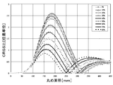
- FIG. 1 was obtained.
- the legend shows the ratio of the elapsed time to the afterheat setting time.
- the diameter of the rounded portion also referred to as the CRSS ratio peak value
- the starting point of the slip dislocation obtained in Experiment 1 is at a position where the diameter of the rounded portion is 185 mm. From these facts, it can be seen that slip dislocations are introduced by thermal stress at the position of the diameter where the value of the CRSS ratio of the rounded portion of the silicon single crystal is maximized in the after heat process.
- the oxygen present as an impurity in the silicon single crystal increases the strength of the silicon single crystal and suppresses the occurrence of slip dislocations in the silicon single crystal, thereby eliminating the rounded portion. It was decided to prevent slip dislocations from being introduced into the rounding part in the after heat process after dislocation growth.
- Example 1 By the CZ method, a cone process, a straight body process, and a rounding process were performed from the raw material melt in the quartz crucible, and then an after heat process was performed to obtain a plurality of silicon single crystals.
- the diameter of the straight body is set to 450 mm
- the length of the rounded part is set to 350 mm
- the lifting speed is 0.5 mm / min
- the set time is 5.0 hours.
- the diameter of the rounded portion where the CRSS ratio of the rounded portion is maximized in the after heat process was obtained in advance by numerical analysis.
- the maximum CRSS ratio in the after heat process was required to be at a position where the diameter of the rounded portion was 185 mm.
- the concentration was adjusted. Specifically, in Example 1, the interstitial oxygen concentration at the obtained position is 8.8 ⁇ 10 17 , 9.6 ⁇ 10 17 , 11.2 ⁇ 10 17 , 12.8 ⁇ 10 17 , and 8.
- a rounding step was performed under control of 8 ⁇ 10 17 [atoms / cm 3 (ASTM '79)] or more. Table 2 shows the results obtained under the above conditions.
- the slip dislocation generation rate of the silicon single crystal grown under the above conditions was 0% in all cases, which was very good as compared with the comparative example.
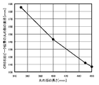
- Example 2 In the rounding process, the length of the rounded part is changed in the range of 350 to 460 mm, and in this case, the interstitial oxygen concentration at the diameter of the rounded part where the CRSS ratio of the rounded part becomes the maximum in the afterheating process is 8.8 ⁇ .
- a silicon single crystal was grown in the same manner as in Example 1 except that the rounding step was performed under control of 10 17 [atoms / cm 3 (ASTM '79)].
- the relationship between the length of a rounding part and the diameter of the rounding part in a CRSS ratio peak position was calculated
- the interstitial oxygen concentration at the position of the diameter of the round portion where the CRSS ratio is maximum is 8.8 ⁇ 10 17 atoms / cm 3 (ASTM '79).
- the length of the rounded portion is set to 450 mm or less, so that slip dislocation can be more reliably suppressed from being introduced into the rounded portion in the after heat process.
- the length of the rounded portion exceeds 450 mm, such as 460 mm, a better result can be obtained than the conventional one.
- Example 3 In the rounding process, the length of the rounding part is changed in the range of 350 to 450 mm. At that time, the interstitial oxygen concentration at the position of the diameter of the rounding part where the CRSS ratio of the rounding part becomes the maximum in the afterheating process is 8.8 ⁇ .
- a rounding step was performed under control of 10 17 [atoms / cm 3 (ASTM '79)].
- the after heat setting time is changed in the range of 1.0 to 4.0 hours, and the height from the melt at the end of the after heat process to the position of the round portion diameter of the CRSS ratio peak position is changed. I let you.
- a silicon single crystal was grown in the same manner as in Example 1 except for the above conditions. Table 4 shows the results obtained under the above conditions.
- the afterheat process setting time is 2.5 hours or more, and further, the distance from the melt at the position of the diameter where the CRSS ratio is the maximum at the end of the afterheat process is 186.0 mm or more. By doing so, it is possible to more reliably suppress slip dislocations from being introduced into the rounding part in the afterheating process.
- the distance from the melt at the position of the diameter at which the CRSS ratio at the end of the after-heating process is less than 2.5 hours (for example, 1.0 hour in Table 4) or after the after-heating process ends is 186. It goes without saying that even if the growth is performed under conditions such as less than 0 mm (for example, 172.0 mm in Table 4), a better result can be obtained than in the past.
- a plurality of silicon single crystals were grown by the CZ method in the same manner as in Example 1 except that the interstitial oxygen concentration in the rounded portion as in Example 1 was not particularly considered.
- the length of the rounded portion was 350 mm, the after heat pulling rate was 0.5 mm / min, and the after heat setting time was 5.0 hours, and the silicon single crystal was grown. The results are shown in Table 5.
- the amount of the silicon melt in the quartz crucible is small, the contact area between the quartz crucible and the silicon melt is reduced, and the free melt surface area increases with the decrease in the crystal diameter.
- the oxygen concentration in the melt decreases. Therefore, the oxygen concentration in the rounded part of the single crystal is usually much lower than that in the straight body part. In the present invention, by improving this and increasing the oxygen concentration in the rounded portion, the occurrence of slip dislocation could be suppressed.
- the present invention is not limited to the above embodiment.
- the above-described embodiment is an exemplification, and the present invention has any configuration that has substantially the same configuration as the technical idea described in the claims of the present invention and that exhibits the same effects. Are included in the technical scope.
Landscapes
- Chemical & Material Sciences (AREA)
- Engineering & Computer Science (AREA)
- Crystallography & Structural Chemistry (AREA)
- Materials Engineering (AREA)
- Metallurgy (AREA)
- Organic Chemistry (AREA)
- Crystals, And After-Treatments Of Crystals (AREA)
Priority Applications (4)
| Application Number | Priority Date | Filing Date | Title |
|---|---|---|---|
| DE112015001883.2T DE112015001883B4 (de) | 2014-05-12 | 2015-03-11 | Verfahren zum Wachsenlassen eines Silizium-Einkristalls |
| US15/305,119 US9988736B2 (en) | 2014-05-12 | 2015-03-11 | Method for growing a silicon single crystal while suppressing a generation of slip dislocations in a tail portion |
| KR1020167031305A KR102105366B1 (ko) | 2014-05-12 | 2015-03-11 | 실리콘 단결정의 육성방법 |
| CN201580027054.XA CN106460227B (zh) | 2014-05-12 | 2015-03-11 | 单晶硅的生长方法 |
Applications Claiming Priority (2)
| Application Number | Priority Date | Filing Date | Title |
|---|---|---|---|
| JP2014098976A JP6070626B2 (ja) | 2014-05-12 | 2014-05-12 | シリコン単結晶の育成方法 |
| JP2014-098976 | 2014-05-12 |
Publications (1)
| Publication Number | Publication Date |
|---|---|
| WO2015173998A1 true WO2015173998A1 (ja) | 2015-11-19 |
Family
ID=54479556
Family Applications (1)
| Application Number | Title | Priority Date | Filing Date |
|---|---|---|---|
| PCT/JP2015/001319 WO2015173998A1 (ja) | 2014-05-12 | 2015-03-11 | シリコン単結晶の育成方法 |
Country Status (6)
Families Citing this family (2)
| Publication number | Priority date | Publication date | Assignee | Title |
|---|---|---|---|---|
| FI3940124T3 (fi) * | 2020-07-14 | 2024-04-03 | Siltronic Ag | Kidekappale yksikiteisestä piistä |
| KR102808187B1 (ko) * | 2021-11-29 | 2025-05-19 | 한국전자통신연구원 | 상이한 네트워크 로봇 컴포넌트들 간의 통신 구성 장치 및 방법 |
Citations (5)
| Publication number | Priority date | Publication date | Assignee | Title |
|---|---|---|---|---|
| JPH11268991A (ja) * | 1998-03-24 | 1999-10-05 | Shin Etsu Handotai Co Ltd | シリコン単結晶の製造方法およびシリコン単結晶 |
| JP2006306640A (ja) * | 2005-04-26 | 2006-11-09 | Komatsu Electronic Metals Co Ltd | シリコンウェーハの製造方法 |
| JP2009274916A (ja) * | 2008-05-15 | 2009-11-26 | Sumco Corp | シリコン単結晶及びその製造方法 |
| JP2010208894A (ja) * | 2009-03-10 | 2010-09-24 | Shin Etsu Handotai Co Ltd | シリコン単結晶の引き上げ方法 |
| JP2010275137A (ja) * | 2009-05-27 | 2010-12-09 | Shin Etsu Handotai Co Ltd | シリコン単結晶の製造方法 |
Family Cites Families (4)
| Publication number | Priority date | Publication date | Assignee | Title |
|---|---|---|---|---|
| US6153A (en) | 1849-03-10 | Loom eoe weaving brussels carpets | ||
| US9A (en) | 1836-08-10 | Thomas Blanchard | Method of riveting plank or made blocks | |
| EP0947611A3 (en) | 1998-03-17 | 2002-03-20 | Shin-Etsu Handotai Company Limited | A method for producing a silicon single crystal and the silicon single crystal produced thereby |
| JP3473477B2 (ja) | 1998-04-07 | 2003-12-02 | 信越半導体株式会社 | シリコン単結晶の製造方法 |
-
2014
- 2014-05-12 JP JP2014098976A patent/JP6070626B2/ja active Active
-
2015
- 2015-03-11 DE DE112015001883.2T patent/DE112015001883B4/de active Active
- 2015-03-11 WO PCT/JP2015/001319 patent/WO2015173998A1/ja active Application Filing
- 2015-03-11 CN CN201580027054.XA patent/CN106460227B/zh active Active
- 2015-03-11 KR KR1020167031305A patent/KR102105366B1/ko active Active
- 2015-03-11 US US15/305,119 patent/US9988736B2/en active Active
Patent Citations (5)
| Publication number | Priority date | Publication date | Assignee | Title |
|---|---|---|---|---|
| JPH11268991A (ja) * | 1998-03-24 | 1999-10-05 | Shin Etsu Handotai Co Ltd | シリコン単結晶の製造方法およびシリコン単結晶 |
| JP2006306640A (ja) * | 2005-04-26 | 2006-11-09 | Komatsu Electronic Metals Co Ltd | シリコンウェーハの製造方法 |
| JP2009274916A (ja) * | 2008-05-15 | 2009-11-26 | Sumco Corp | シリコン単結晶及びその製造方法 |
| JP2010208894A (ja) * | 2009-03-10 | 2010-09-24 | Shin Etsu Handotai Co Ltd | シリコン単結晶の引き上げ方法 |
| JP2010275137A (ja) * | 2009-05-27 | 2010-12-09 | Shin Etsu Handotai Co Ltd | シリコン単結晶の製造方法 |
Also Published As
| Publication number | Publication date |
|---|---|
| CN106460227B (zh) | 2019-03-22 |
| CN106460227A (zh) | 2017-02-22 |
| KR102105366B1 (ko) | 2020-04-28 |
| DE112015001883B4 (de) | 2022-03-17 |
| JP2015214460A (ja) | 2015-12-03 |
| DE112015001883T5 (de) | 2016-12-29 |
| US9988736B2 (en) | 2018-06-05 |
| US20170044685A1 (en) | 2017-02-16 |
| JP6070626B2 (ja) | 2017-02-01 |
| KR20170009853A (ko) | 2017-01-25 |
Similar Documents
| Publication | Publication Date | Title |
|---|---|---|
| Wong et al. | Development of grain structures of multi-crystalline silicon from randomly orientated seeds in directional solidification | |
| JP4151580B2 (ja) | シリコン単結晶の製造方法並びにシリコン単結晶とシリコンウエーハ | |
| JP4142332B2 (ja) | 単結晶シリコンの製造方法、単結晶シリコンウェーハの製造方法、単結晶シリコン製造用種結晶、単結晶シリコンインゴットおよび単結晶シリコンウェーハ | |
| US10100430B2 (en) | Method for growing silicon single crystal | |
| CN107109686A (zh) | 用于制造单晶硅锭的方法、以及通过该制备方法制备的单晶硅锭 | |
| JP2009292659A (ja) | シリコン単結晶育成における肩形成方法 | |
| JP2009057270A (ja) | シリコン単結晶の引上方法 | |
| JP6070626B2 (ja) | シリコン単結晶の育成方法 | |
| JP2016183072A (ja) | シリコン単結晶の製造方法 | |
| JP2973917B2 (ja) | 単結晶引き上げ方法 | |
| US20120279438A1 (en) | Methods for producing single crystal silicon ingots with reduced incidence of dislocations | |
| US20090038537A1 (en) | Method of pulling up silicon single crystal | |
| JP2525300B2 (ja) | シリコン単結晶の製造方法 | |
| JP4407188B2 (ja) | シリコンウェーハの製造方法およびシリコンウェーハ | |
| JP2022504609A (ja) | インゴットの品質を向上するためのシリコン融液中のドーパント濃度制御 | |
| JP2009292662A (ja) | シリコン単結晶育成における肩形成方法 | |
| JP2010275137A (ja) | シリコン単結晶の製造方法 | |
| JP2003246695A (ja) | 高濃度にドーピングされたシリコン単結晶の製造方法 | |
| JP2011251892A (ja) | InP単結晶およびその製造方法 | |
| JP7310339B2 (ja) | ニオブ酸リチウム単結晶の育成方法 | |
| JP5954247B2 (ja) | シリコン単結晶の製造方法 | |
| JP2004175620A (ja) | 単結晶の製造方法 | |
| KR101173764B1 (ko) | 무전위 실리콘 단결정의 제조 방법 | |
| JP6488975B2 (ja) | シリコン単結晶の引上げ方法 | |
| JP5070916B2 (ja) | シリコン単結晶およびシリコンウェーハ |
Legal Events
| Date | Code | Title | Description |
|---|---|---|---|
| 121 | Ep: the epo has been informed by wipo that ep was designated in this application |
Ref document number: 15792861 Country of ref document: EP Kind code of ref document: A1 |
|
| WWE | Wipo information: entry into national phase |
Ref document number: 15305119 Country of ref document: US |
|
| ENP | Entry into the national phase |
Ref document number: 20167031305 Country of ref document: KR Kind code of ref document: A |
|
| WWE | Wipo information: entry into national phase |
Ref document number: 112015001883 Country of ref document: DE |
|
| 122 | Ep: pct application non-entry in european phase |
Ref document number: 15792861 Country of ref document: EP Kind code of ref document: A1 |