WO2015166754A1 - Semiconductor device - Google Patents
Semiconductor device Download PDFInfo
- Publication number
- WO2015166754A1 WO2015166754A1 PCT/JP2015/059968 JP2015059968W WO2015166754A1 WO 2015166754 A1 WO2015166754 A1 WO 2015166754A1 JP 2015059968 W JP2015059968 W JP 2015059968W WO 2015166754 A1 WO2015166754 A1 WO 2015166754A1
- Authority
- WO
- WIPO (PCT)
- Prior art keywords
- cell
- region
- semiconductor device
- base region
- trench
- Prior art date
Links
- 239000004065 semiconductor Substances 0.000 title claims description 47
- 238000009792 diffusion process Methods 0.000 claims description 24
- 230000001681 protective effect Effects 0.000 claims description 23
- 230000015556 catabolic process Effects 0.000 abstract description 33
- 238000000034 method Methods 0.000 abstract description 21
- 239000010410 layer Substances 0.000 description 90
- 230000002093 peripheral effect Effects 0.000 description 28
- HBMJWWWQQXIZIP-UHFFFAOYSA-N silicon carbide Chemical compound [Si+]#[C-] HBMJWWWQQXIZIP-UHFFFAOYSA-N 0.000 description 21
- 230000005684 electric field Effects 0.000 description 20
- 229910010271 silicon carbide Inorganic materials 0.000 description 19
- 239000012535 impurity Substances 0.000 description 16
- 238000004519 manufacturing process Methods 0.000 description 15
- VYPSYNLAJGMNEJ-UHFFFAOYSA-N Silicium dioxide Chemical compound O=[Si]=O VYPSYNLAJGMNEJ-UHFFFAOYSA-N 0.000 description 14
- 229910052814 silicon oxide Inorganic materials 0.000 description 14
- 239000000758 substrate Substances 0.000 description 13
- 238000005530 etching Methods 0.000 description 11
- 239000011229 interlayer Substances 0.000 description 11
- 230000000694 effects Effects 0.000 description 10
- 238000005468 ion implantation Methods 0.000 description 10
- 238000002513 implantation Methods 0.000 description 6
- 230000001629 suppression Effects 0.000 description 6
- 230000006378 damage Effects 0.000 description 5
- 230000004048 modification Effects 0.000 description 5
- 238000012986 modification Methods 0.000 description 5
- 238000001020 plasma etching Methods 0.000 description 5
- IJGRMHOSHXDMSA-UHFFFAOYSA-N Atomic nitrogen Chemical compound N#N IJGRMHOSHXDMSA-UHFFFAOYSA-N 0.000 description 4
- 238000010586 diagram Methods 0.000 description 4
- 239000000463 material Substances 0.000 description 4
- 230000008569 process Effects 0.000 description 4
- JMASRVWKEDWRBT-UHFFFAOYSA-N Gallium nitride Chemical compound [Ga]#N JMASRVWKEDWRBT-UHFFFAOYSA-N 0.000 description 3
- PXHVJJICTQNCMI-UHFFFAOYSA-N Nickel Chemical compound [Ni] PXHVJJICTQNCMI-UHFFFAOYSA-N 0.000 description 3
- 239000010432 diamond Substances 0.000 description 3
- 229910003460 diamond Inorganic materials 0.000 description 3
- 238000010438 heat treatment Methods 0.000 description 3
- 229910052751 metal Inorganic materials 0.000 description 3
- 239000002184 metal Substances 0.000 description 3
- 229910000838 Al alloy Inorganic materials 0.000 description 2
- XKRFYHLGVUSROY-UHFFFAOYSA-N Argon Chemical compound [Ar] XKRFYHLGVUSROY-UHFFFAOYSA-N 0.000 description 2
- VEXZGXHMUGYJMC-UHFFFAOYSA-N Hydrochloric acid Chemical compound Cl VEXZGXHMUGYJMC-UHFFFAOYSA-N 0.000 description 2
- MHAJPDPJQMAIIY-UHFFFAOYSA-N Hydrogen peroxide Chemical compound OO MHAJPDPJQMAIIY-UHFFFAOYSA-N 0.000 description 2
- QAOWNCQODCNURD-UHFFFAOYSA-N Sulfuric acid Chemical compound OS(O)(=O)=O QAOWNCQODCNURD-UHFFFAOYSA-N 0.000 description 2
- 238000000137 annealing Methods 0.000 description 2
- 230000008859 change Effects 0.000 description 2
- 238000005229 chemical vapour deposition Methods 0.000 description 2
- 239000007772 electrode material Substances 0.000 description 2
- 238000004518 low pressure chemical vapour deposition Methods 0.000 description 2
- 229910052757 nitrogen Inorganic materials 0.000 description 2
- 238000000059 patterning Methods 0.000 description 2
- 229910021420 polycrystalline silicon Inorganic materials 0.000 description 2
- 230000009467 reduction Effects 0.000 description 2
- 229910002601 GaN Inorganic materials 0.000 description 1
- GRYLNZFGIOXLOG-UHFFFAOYSA-N Nitric acid Chemical compound O[N+]([O-])=O GRYLNZFGIOXLOG-UHFFFAOYSA-N 0.000 description 1
- OAICVXFJPJFONN-UHFFFAOYSA-N Phosphorus Chemical compound [P] OAICVXFJPJFONN-UHFFFAOYSA-N 0.000 description 1
- XUIMIQQOPSSXEZ-UHFFFAOYSA-N Silicon Chemical compound [Si] XUIMIQQOPSSXEZ-UHFFFAOYSA-N 0.000 description 1
- 230000003213 activating effect Effects 0.000 description 1
- 229910052782 aluminium Inorganic materials 0.000 description 1
- XAGFODPZIPBFFR-UHFFFAOYSA-N aluminium Chemical compound [Al] XAGFODPZIPBFFR-UHFFFAOYSA-N 0.000 description 1
- 229910052786 argon Inorganic materials 0.000 description 1
- 230000015572 biosynthetic process Effects 0.000 description 1
- 239000000969 carrier Substances 0.000 description 1
- 238000000151 deposition Methods 0.000 description 1
- 239000002019 doping agent Substances 0.000 description 1
- 230000005669 field effect Effects 0.000 description 1
- 239000007789 gas Substances 0.000 description 1
- 239000011261 inert gas Substances 0.000 description 1
- 238000009413 insulation Methods 0.000 description 1
- 239000011159 matrix material Substances 0.000 description 1
- 229910044991 metal oxide Inorganic materials 0.000 description 1
- 150000004706 metal oxides Chemical class 0.000 description 1
- 239000011259 mixed solution Substances 0.000 description 1
- 229910052759 nickel Inorganic materials 0.000 description 1
- 229910017604 nitric acid Inorganic materials 0.000 description 1
- 230000001590 oxidative effect Effects 0.000 description 1
- 229910052698 phosphorus Inorganic materials 0.000 description 1
- 239000011574 phosphorus Substances 0.000 description 1
- 238000000206 photolithography Methods 0.000 description 1
- 229920005591 polysilicon Polymers 0.000 description 1
- 230000001737 promoting effect Effects 0.000 description 1
- 229910021332 silicide Inorganic materials 0.000 description 1
- FVBUAEGBCNSCDD-UHFFFAOYSA-N silicide(4-) Chemical compound [Si-4] FVBUAEGBCNSCDD-UHFFFAOYSA-N 0.000 description 1
- 229910052710 silicon Inorganic materials 0.000 description 1
- 239000010703 silicon Substances 0.000 description 1
- 238000001039 wet etching Methods 0.000 description 1
Images


Classifications
-
- H—ELECTRICITY
- H01—ELECTRIC ELEMENTS
- H01L—SEMICONDUCTOR DEVICES NOT COVERED BY CLASS H10
- H01L29/00—Semiconductor devices adapted for rectifying, amplifying, oscillating or switching, or capacitors or resistors with at least one potential-jump barrier or surface barrier, e.g. PN junction depletion layer or carrier concentration layer; Details of semiconductor bodies or of electrodes thereof ; Multistep manufacturing processes therefor
- H01L29/02—Semiconductor bodies ; Multistep manufacturing processes therefor
- H01L29/06—Semiconductor bodies ; Multistep manufacturing processes therefor characterised by their shape; characterised by the shapes, relative sizes, or dispositions of the semiconductor regions ; characterised by the concentration or distribution of impurities within semiconductor regions
- H01L29/0684—Semiconductor bodies ; Multistep manufacturing processes therefor characterised by their shape; characterised by the shapes, relative sizes, or dispositions of the semiconductor regions ; characterised by the concentration or distribution of impurities within semiconductor regions characterised by the shape, relative sizes or dispositions of the semiconductor regions or junctions between the regions
- H01L29/0692—Surface layout
- H01L29/0696—Surface layout of cellular field-effect devices, e.g. multicellular DMOS transistors or IGBTs
-
- H—ELECTRICITY
- H01—ELECTRIC ELEMENTS
- H01L—SEMICONDUCTOR DEVICES NOT COVERED BY CLASS H10
- H01L29/00—Semiconductor devices adapted for rectifying, amplifying, oscillating or switching, or capacitors or resistors with at least one potential-jump barrier or surface barrier, e.g. PN junction depletion layer or carrier concentration layer; Details of semiconductor bodies or of electrodes thereof ; Multistep manufacturing processes therefor
- H01L29/02—Semiconductor bodies ; Multistep manufacturing processes therefor
- H01L29/06—Semiconductor bodies ; Multistep manufacturing processes therefor characterised by their shape; characterised by the shapes, relative sizes, or dispositions of the semiconductor regions ; characterised by the concentration or distribution of impurities within semiconductor regions
- H01L29/0603—Semiconductor bodies ; Multistep manufacturing processes therefor characterised by their shape; characterised by the shapes, relative sizes, or dispositions of the semiconductor regions ; characterised by the concentration or distribution of impurities within semiconductor regions characterised by particular constructional design considerations, e.g. for preventing surface leakage, for controlling electric field concentration or for internal isolations regions
- H01L29/0607—Semiconductor bodies ; Multistep manufacturing processes therefor characterised by their shape; characterised by the shapes, relative sizes, or dispositions of the semiconductor regions ; characterised by the concentration or distribution of impurities within semiconductor regions characterised by particular constructional design considerations, e.g. for preventing surface leakage, for controlling electric field concentration or for internal isolations regions for preventing surface leakage or controlling electric field concentration
- H01L29/0611—Semiconductor bodies ; Multistep manufacturing processes therefor characterised by their shape; characterised by the shapes, relative sizes, or dispositions of the semiconductor regions ; characterised by the concentration or distribution of impurities within semiconductor regions characterised by particular constructional design considerations, e.g. for preventing surface leakage, for controlling electric field concentration or for internal isolations regions for preventing surface leakage or controlling electric field concentration for increasing or controlling the breakdown voltage of reverse biased devices
- H01L29/0615—Semiconductor bodies ; Multistep manufacturing processes therefor characterised by their shape; characterised by the shapes, relative sizes, or dispositions of the semiconductor regions ; characterised by the concentration or distribution of impurities within semiconductor regions characterised by particular constructional design considerations, e.g. for preventing surface leakage, for controlling electric field concentration or for internal isolations regions for preventing surface leakage or controlling electric field concentration for increasing or controlling the breakdown voltage of reverse biased devices by the doping profile or the shape or the arrangement of the PN junction, or with supplementary regions, e.g. junction termination extension [JTE]
- H01L29/0619—Semiconductor bodies ; Multistep manufacturing processes therefor characterised by their shape; characterised by the shapes, relative sizes, or dispositions of the semiconductor regions ; characterised by the concentration or distribution of impurities within semiconductor regions characterised by particular constructional design considerations, e.g. for preventing surface leakage, for controlling electric field concentration or for internal isolations regions for preventing surface leakage or controlling electric field concentration for increasing or controlling the breakdown voltage of reverse biased devices by the doping profile or the shape or the arrangement of the PN junction, or with supplementary regions, e.g. junction termination extension [JTE] with a supplementary region doped oppositely to or in rectifying contact with the semiconductor containing or contacting region, e.g. guard rings with PN or Schottky junction
- H01L29/0623—Buried supplementary region, e.g. buried guard ring
-
- H—ELECTRICITY
- H01—ELECTRIC ELEMENTS
- H01L—SEMICONDUCTOR DEVICES NOT COVERED BY CLASS H10
- H01L29/00—Semiconductor devices adapted for rectifying, amplifying, oscillating or switching, or capacitors or resistors with at least one potential-jump barrier or surface barrier, e.g. PN junction depletion layer or carrier concentration layer; Details of semiconductor bodies or of electrodes thereof ; Multistep manufacturing processes therefor
- H01L29/02—Semiconductor bodies ; Multistep manufacturing processes therefor
- H01L29/06—Semiconductor bodies ; Multistep manufacturing processes therefor characterised by their shape; characterised by the shapes, relative sizes, or dispositions of the semiconductor regions ; characterised by the concentration or distribution of impurities within semiconductor regions
- H01L29/08—Semiconductor bodies ; Multistep manufacturing processes therefor characterised by their shape; characterised by the shapes, relative sizes, or dispositions of the semiconductor regions ; characterised by the concentration or distribution of impurities within semiconductor regions with semiconductor regions connected to an electrode carrying current to be rectified, amplified or switched and such electrode being part of a semiconductor device which comprises three or more electrodes
- H01L29/0843—Source or drain regions of field-effect devices
- H01L29/0847—Source or drain regions of field-effect devices of field-effect transistors with insulated gate
- H01L29/0852—Source or drain regions of field-effect devices of field-effect transistors with insulated gate of DMOS transistors
- H01L29/0856—Source regions
- H01L29/0865—Disposition
-
- H—ELECTRICITY
- H01—ELECTRIC ELEMENTS
- H01L—SEMICONDUCTOR DEVICES NOT COVERED BY CLASS H10
- H01L29/00—Semiconductor devices adapted for rectifying, amplifying, oscillating or switching, or capacitors or resistors with at least one potential-jump barrier or surface barrier, e.g. PN junction depletion layer or carrier concentration layer; Details of semiconductor bodies or of electrodes thereof ; Multistep manufacturing processes therefor
- H01L29/02—Semiconductor bodies ; Multistep manufacturing processes therefor
- H01L29/06—Semiconductor bodies ; Multistep manufacturing processes therefor characterised by their shape; characterised by the shapes, relative sizes, or dispositions of the semiconductor regions ; characterised by the concentration or distribution of impurities within semiconductor regions
- H01L29/08—Semiconductor bodies ; Multistep manufacturing processes therefor characterised by their shape; characterised by the shapes, relative sizes, or dispositions of the semiconductor regions ; characterised by the concentration or distribution of impurities within semiconductor regions with semiconductor regions connected to an electrode carrying current to be rectified, amplified or switched and such electrode being part of a semiconductor device which comprises three or more electrodes
- H01L29/0843—Source or drain regions of field-effect devices
- H01L29/0847—Source or drain regions of field-effect devices of field-effect transistors with insulated gate
- H01L29/0852—Source or drain regions of field-effect devices of field-effect transistors with insulated gate of DMOS transistors
- H01L29/0856—Source regions
- H01L29/0869—Shape
-
- H—ELECTRICITY
- H01—ELECTRIC ELEMENTS
- H01L—SEMICONDUCTOR DEVICES NOT COVERED BY CLASS H10
- H01L29/00—Semiconductor devices adapted for rectifying, amplifying, oscillating or switching, or capacitors or resistors with at least one potential-jump barrier or surface barrier, e.g. PN junction depletion layer or carrier concentration layer; Details of semiconductor bodies or of electrodes thereof ; Multistep manufacturing processes therefor
- H01L29/02—Semiconductor bodies ; Multistep manufacturing processes therefor
- H01L29/12—Semiconductor bodies ; Multistep manufacturing processes therefor characterised by the materials of which they are formed
- H01L29/16—Semiconductor bodies ; Multistep manufacturing processes therefor characterised by the materials of which they are formed including, apart from doping materials or other impurities, only elements of Group IV of the Periodic System
- H01L29/1608—Silicon carbide
-
- H—ELECTRICITY
- H01—ELECTRIC ELEMENTS
- H01L—SEMICONDUCTOR DEVICES NOT COVERED BY CLASS H10
- H01L29/00—Semiconductor devices adapted for rectifying, amplifying, oscillating or switching, or capacitors or resistors with at least one potential-jump barrier or surface barrier, e.g. PN junction depletion layer or carrier concentration layer; Details of semiconductor bodies or of electrodes thereof ; Multistep manufacturing processes therefor
- H01L29/40—Electrodes ; Multistep manufacturing processes therefor
- H01L29/41—Electrodes ; Multistep manufacturing processes therefor characterised by their shape, relative sizes or dispositions
- H01L29/417—Electrodes ; Multistep manufacturing processes therefor characterised by their shape, relative sizes or dispositions carrying the current to be rectified, amplified or switched
- H01L29/41725—Source or drain electrodes for field effect devices
- H01L29/41741—Source or drain electrodes for field effect devices for vertical or pseudo-vertical devices
-
- H—ELECTRICITY
- H01—ELECTRIC ELEMENTS
- H01L—SEMICONDUCTOR DEVICES NOT COVERED BY CLASS H10
- H01L29/00—Semiconductor devices adapted for rectifying, amplifying, oscillating or switching, or capacitors or resistors with at least one potential-jump barrier or surface barrier, e.g. PN junction depletion layer or carrier concentration layer; Details of semiconductor bodies or of electrodes thereof ; Multistep manufacturing processes therefor
- H01L29/40—Electrodes ; Multistep manufacturing processes therefor
- H01L29/41—Electrodes ; Multistep manufacturing processes therefor characterised by their shape, relative sizes or dispositions
- H01L29/423—Electrodes ; Multistep manufacturing processes therefor characterised by their shape, relative sizes or dispositions not carrying the current to be rectified, amplified or switched
- H01L29/42312—Gate electrodes for field effect devices
- H01L29/42316—Gate electrodes for field effect devices for field-effect transistors
- H01L29/4232—Gate electrodes for field effect devices for field-effect transistors with insulated gate
- H01L29/42356—Disposition, e.g. buried gate electrode
- H01L29/4236—Disposition, e.g. buried gate electrode within a trench, e.g. trench gate electrode, groove gate electrode
-
- H—ELECTRICITY
- H01—ELECTRIC ELEMENTS
- H01L—SEMICONDUCTOR DEVICES NOT COVERED BY CLASS H10
- H01L29/00—Semiconductor devices adapted for rectifying, amplifying, oscillating or switching, or capacitors or resistors with at least one potential-jump barrier or surface barrier, e.g. PN junction depletion layer or carrier concentration layer; Details of semiconductor bodies or of electrodes thereof ; Multistep manufacturing processes therefor
- H01L29/40—Electrodes ; Multistep manufacturing processes therefor
- H01L29/41—Electrodes ; Multistep manufacturing processes therefor characterised by their shape, relative sizes or dispositions
- H01L29/423—Electrodes ; Multistep manufacturing processes therefor characterised by their shape, relative sizes or dispositions not carrying the current to be rectified, amplified or switched
- H01L29/42312—Gate electrodes for field effect devices
- H01L29/42316—Gate electrodes for field effect devices for field-effect transistors
- H01L29/4232—Gate electrodes for field effect devices for field-effect transistors with insulated gate
- H01L29/42372—Gate electrodes for field effect devices for field-effect transistors with insulated gate characterised by the conducting layer, e.g. the length, the sectional shape or the lay-out
- H01L29/4238—Gate electrodes for field effect devices for field-effect transistors with insulated gate characterised by the conducting layer, e.g. the length, the sectional shape or the lay-out characterised by the surface lay-out
-
- H—ELECTRICITY
- H01—ELECTRIC ELEMENTS
- H01L—SEMICONDUCTOR DEVICES NOT COVERED BY CLASS H10
- H01L29/00—Semiconductor devices adapted for rectifying, amplifying, oscillating or switching, or capacitors or resistors with at least one potential-jump barrier or surface barrier, e.g. PN junction depletion layer or carrier concentration layer; Details of semiconductor bodies or of electrodes thereof ; Multistep manufacturing processes therefor
- H01L29/66—Types of semiconductor device ; Multistep manufacturing processes therefor
- H01L29/68—Types of semiconductor device ; Multistep manufacturing processes therefor controllable by only the electric current supplied, or only the electric potential applied, to an electrode which does not carry the current to be rectified, amplified or switched
- H01L29/70—Bipolar devices
- H01L29/72—Transistor-type devices, i.e. able to continuously respond to applied control signals
- H01L29/739—Transistor-type devices, i.e. able to continuously respond to applied control signals controlled by field-effect, e.g. bipolar static induction transistors [BSIT]
- H01L29/7393—Insulated gate bipolar mode transistors, i.e. IGBT; IGT; COMFET
- H01L29/7395—Vertical transistors, e.g. vertical IGBT
- H01L29/7396—Vertical transistors, e.g. vertical IGBT with a non planar surface, e.g. with a non planar gate or with a trench or recess or pillar in the surface of the emitter, base or collector region for improving current density or short circuiting the emitter and base regions
- H01L29/7397—Vertical transistors, e.g. vertical IGBT with a non planar surface, e.g. with a non planar gate or with a trench or recess or pillar in the surface of the emitter, base or collector region for improving current density or short circuiting the emitter and base regions and a gate structure lying on a slanted or vertical surface or formed in a groove, e.g. trench gate IGBT
-
- H—ELECTRICITY
- H01—ELECTRIC ELEMENTS
- H01L—SEMICONDUCTOR DEVICES NOT COVERED BY CLASS H10
- H01L29/00—Semiconductor devices adapted for rectifying, amplifying, oscillating or switching, or capacitors or resistors with at least one potential-jump barrier or surface barrier, e.g. PN junction depletion layer or carrier concentration layer; Details of semiconductor bodies or of electrodes thereof ; Multistep manufacturing processes therefor
- H01L29/66—Types of semiconductor device ; Multistep manufacturing processes therefor
- H01L29/68—Types of semiconductor device ; Multistep manufacturing processes therefor controllable by only the electric current supplied, or only the electric potential applied, to an electrode which does not carry the current to be rectified, amplified or switched
- H01L29/76—Unipolar devices, e.g. field effect transistors
- H01L29/772—Field effect transistors
- H01L29/78—Field effect transistors with field effect produced by an insulated gate
- H01L29/7801—DMOS transistors, i.e. MISFETs with a channel accommodating body or base region adjoining a drain drift region
- H01L29/7802—Vertical DMOS transistors, i.e. VDMOS transistors
- H01L29/7813—Vertical DMOS transistors, i.e. VDMOS transistors with trench gate electrode, e.g. UMOS transistors
Landscapes
- Engineering & Computer Science (AREA)
- Microelectronics & Electronic Packaging (AREA)
- Power Engineering (AREA)
- Physics & Mathematics (AREA)
- Ceramic Engineering (AREA)
- Condensed Matter Physics & Semiconductors (AREA)
- General Physics & Mathematics (AREA)
- Computer Hardware Design (AREA)
- Electrodes Of Semiconductors (AREA)
Abstract
Description
<構成>
以下、本実施の形態1に係る半導体装置は、炭化珪素(SiC)半導体装置であってトレンチゲート型MOSFETである場合を例にして説明する。図1は、本実施の形態1に係るMOSFETの全体構成を示す平面図である。 <
<Configuration>
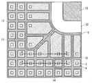
Hereinafter, the case where the semiconductor device according to the first embodiment is a silicon carbide (SiC) semiconductor device and is a trench gate type MOSFET will be described as an example. FIG. 1 is a plan view showing the overall configuration of the MOSFET according to the first embodiment.
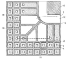
図6は、関連MOSFETの一部の構成を図2と同様に示す平面図である。以下、関連MOSFETにおいて、以上で説明した構成要素と同一ものについては同じ参照符号を付して、関連MOSFETのうち上述の構成要素と異なる構成要素と問題点とについて説明する。 <Related MOSFET>
FIG. 6 is a plan view showing a part of the structure of the related MOSFET in the same manner as FIG. Hereinafter, in the related MOSFET, the same components as those described above are denoted by the same reference numerals, and components and problems different from the above-described components of the related MOSFET will be described.
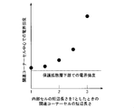
そこで、発明者は、これを利用することで、平面視においてゲートパッド13の曲部に対向する領域41に配設されたセル中心部での空乏層厚の減少を抑制することを想起した。 <Dimensions of MOSFET according to
Therefore, the inventor has conceived that by using this, a reduction in the thickness of the depletion layer at the center of the cell disposed in the
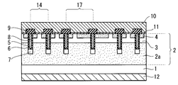
次に、本実施の形態1に係るMOSFETの製造方法について説明する。図10~図16は、当該製造方法の工程を示す図であり、具体的には、図5と同様に図2のB-B線に沿った断面図である。 <Manufacturing method>
Next, a method for manufacturing the MOSFET according to the first embodiment will be described. 10 to 16 are diagrams showing the steps of the manufacturing method. Specifically, FIG. 10 to FIG. 16 are cross-sectional views along the line BB in FIG. 2, as in FIG.
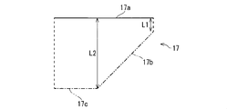
以上に構成された本実施の形態1に係るMOSFETでは、コーナーセル17の平面視での外郭形状において、最も長い辺と、当該辺に対向する各辺との間の各最短距離のうち、最も長い距離が、内部セル14の均等な一辺または短辺の長さの2倍以下となるように構成される。これにより、コーナーセル17においても内部セル14と同等の空乏層厚を得ることができるため、アバランシェ破壊を抑制することができる。 <Effect>
In the MOSFET according to the first embodiment configured as described above, the outermost shape of the
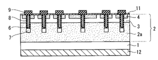
なお、以上の説明では、ドリフト層2aと、バッファ層であるSiC基板1とが同じ導電型を有する構造のMOSFETについて述べたが、ドリフト層2aとSiC基板1とが異なる導電型を有する構造のIGBTに対しても適用可能である。例えば、図4及び図5に示した構成において、SiC基板1のn導電型をp導電型に代えればIGBTの構成となる。そして、そのような構成では、MOSFETのソース領域4及びソース電極10は、それぞれIGBTのエミッタ領域及びエミッタ電極に対応し、MOSFETのドレイン電極12はコレクタ電極に対応することになる。 <Modification>
Although the
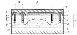
<構成>
図19は、本発明の実施の形態2に係るMOSFETの構成の一部を、図2と同様に示す平面図である。図20は、本実施の形態2に係るMOSFETの構成の一部を示す断面図であり、具体的には、図19のD-D線に沿った断面図であり、内部セル14及びコーナーセル17の断面構成を示している。以下、本実施の形態2に係るMOSFETにおいて、以上で説明した構成要素と同一または類似するものについては同じ参照符号を付し、異なる部分について主に説明する。 <
<Configuration>
FIG. 19 is a plan view showing a part of the configuration of the MOSFET according to the second embodiment of the present invention in the same manner as FIG. FIG. 20 is a cross-sectional view showing a part of the structure of the MOSFET according to the second embodiment. Specifically, it is a cross-sectional view along the line DD in FIG. 19, and shows the
図5及び図20を参照して、本実施の形態2に係るコーナーセル19の効果について説明する。コーナーセル17,19が配設された内側コーナー部では、電界状態がセル領域31の内部や他の外周部とは異なる状態となっているため、空乏層の延びが異なる。これに伴って、ソース領域4を備える実施の形態1のコーナーセル17では、ベース領域3内で上部のソース領域4から延びる空乏層と下部のドリフト層2aから延びる空乏層とが接触し、ドリフト層2aとソース領域4との間の絶縁が破れてキャリアが流れるパンチスルー現象が生じる可能性が多少ある。 <Effect>
The effect of the
<構成>
図21は、本実施の形態3に係るMOSFETの構成の一部を、図20と同様に示す断面図である。以下、本実施の形態3に係るMOSFETにおいて、以上で説明した構成要素と同一または類似するものについては同じ参照符号を付し、異なる部分について主に説明する。 <
<Configuration>
FIG. 21 is a cross-sectional view showing a part of the configuration of the MOSFET according to the third embodiment in the same manner as FIG. Hereinafter, in the MOSFET according to the third embodiment, the same or similar components as those described above are denoted by the same reference numerals, and different portions will be mainly described.
図21を参照して、本実施の形態3に係るコーナーセル20の効果について説明する。コーナーセル20などの各種セルにアバランシェ電流が流れる経路は、ドレイン電極12とソース電極10との間である。このため、耐圧の低いコーナーセル20において、ソース電極10と、ソース領域4及びベース領域3とが電気的に絶縁されている本実施の形態3によれば、全体の耐圧を向上させることができる。また、本実施の形態3に係るMOSFETの製造方法としては、実施の形態1の図15の工程において、コーナーセル20における層間絶縁膜9を除去しないようにするだけでよく、容易に実現することができる。また、本実施の形態3に係るコーナーセル20は、単独でMOSFETの機能を有さないが、それに伴うオン抵抗の増加分は、実施の形態2と同様、実質的にほぼ無視できる程度である。 <Effect>
The effect of the
<構成>
図22は、本発明の実施の形態4に係るMOSFETの構成の一部を、図2と同様に示す平面図である。図23は、本実施の形態4に係るMOSFETの構成の一部を、図20と同様に示す断面図であり、具体的には図22のC-C線に沿った断面図である。以下、本実施の形態4に係るMOSFETにおいて、以上で説明した構成要素と同一または類似するものについては同じ参照符号を付し、異なる部分について主に説明する。 <
<Configuration>
FIG. 22 is a plan view showing a part of the configuration of the MOSFET according to the fourth embodiment of the present invention in the same manner as FIG. FIG. 23 is a cross-sectional view showing a part of the configuration of the MOSFET according to the fourth embodiment in the same manner as in FIG. 20, and more specifically, a cross-sectional view taken along the line CC in FIG. Hereinafter, in the MOSFET according to the fourth embodiment, the same or similar components as those described above are denoted by the same reference numerals, and different portions will be mainly described.
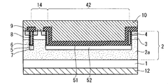
図21を参照して、本実施の形態4に係る無効領域42の効果について説明する。コーナーセル17などが配設される領域41(図3)がセル領域31に占める割合は実質的に無視できる程度である。しかし、当該領域41はこれまで説明してきたようにアバランシェ破壊が生じやすいため通常のセルを配設することが難しい。そこで、当該領域41全体をトレンチ51とし、その底部に保護拡散層52を設けることで当該領域41での耐圧低下を防ぎ、全体の耐圧を向上させることができる。 <Effect>
With reference to FIG. 21, the effect of the
Claims (9)
- ゲートパッドと、
平面視において前記ゲートパッドの角部に対向する領域に配設された第1セルと、
平面視において前記第1セルに対して前記ゲートパッドと逆側の領域に配設された第2セルと
を備え、
前記第1及び第2セルのそれぞれは、
第1導電型の半導体層と、
前記半導体層の上部に形成された第2導電型のベース領域と、
前記ベース領域を貫通して前記ベース領域下の前記半導体層に達するトレンチ内に、ゲート絶縁膜を介して配設されるとともに、前記第1及び第2セルの平面視での外郭形状に対応するパターンを有し、かつ、前記ゲートパッドと電気的に接続されたゲート電極と、
前記トレンチの底部に形成された第2導電型の保護拡散層と
を備え、
前記第1及び第2セルのうち少なくとも前記第2セルは、
前記ベース領域の上部のうち、前記ゲート絶縁膜に隣接する部分に形成された第1導電型のソース領域と、
前記ベース領域及び前記ソース領域と電気的に接続されたソース電極と
をさらに備え、
前記第1及び第2セルの前記外郭形状は、四角形以上の多角形状であり、
前記第1セルの前記外郭形状において、最も長い辺と、当該辺に対向する各辺との間の各最短距離のうち、最も長い距離が、前記第2セルの均等な一辺または短辺の長さの2倍以下である、半導体装置。 Gate pad,
A first cell disposed in a region facing a corner of the gate pad in plan view;
A second cell disposed in a region opposite to the gate pad with respect to the first cell in plan view;
Each of the first and second cells is
A first conductivity type semiconductor layer;
A second conductivity type base region formed on the semiconductor layer;
A gate insulating film is disposed in a trench that penetrates the base region and reaches the semiconductor layer below the base region, and corresponds to the outer shape of the first and second cells in plan view. A gate electrode having a pattern and electrically connected to the gate pad;
A protective diffusion layer of a second conductivity type formed at the bottom of the trench,
At least the second cell of the first and second cells is
A source region of a first conductivity type formed in a portion of the upper portion of the base region adjacent to the gate insulating film;
A source electrode electrically connected to the base region and the source region;
The outline shape of the first and second cells is a quadrilateral or more polygonal shape,
In the outline shape of the first cell, the longest distance among the shortest distances between the longest side and each side facing the side is the length of an equal side or short side of the second cell. A semiconductor device that is twice or less of - 請求項1に記載の半導体装置であって、
前記第1セルの前記多角形状の頂点は、前記第2セルの前記多角形状の頂点よりも多い、半導体装置。 The semiconductor device according to claim 1,
The semiconductor device, wherein the number of vertices of the polygonal shape of the first cell is greater than the number of vertices of the polygonal shape of the second cell. - 請求項1に記載の半導体装置であって、
前記第1セルの前記多角形状の内角は全て90°以上である、半導体装置。 The semiconductor device according to claim 1,
The semiconductor device in which all the internal angles of the polygonal shape of the first cell are 90 ° or more. - 請求項1に記載の半導体装置であって、
前記第1セルは前記ソース領域を備えない、半導体装置。 The semiconductor device according to claim 1,
The semiconductor device, wherein the first cell does not include the source region. - 請求項1に記載の半導体装置であって、
前記第1セルにおいて、前記ソース電極と、前記ベース領域及び前記ソース領域とが電気的に絶縁されている、半導体装置。 The semiconductor device according to claim 1,
In the first cell, the source electrode, the base region, and the source region are electrically insulated from each other. - 請求項1に記載の半導体装置であって、
前記第1セルは、
前記ソース領域及び前記ゲート電極をさらに備え、単独でスイッチング素子の機能を有する、半導体装置。 The semiconductor device according to claim 1,
The first cell is
A semiconductor device further comprising the source region and the gate electrode and independently having a function of a switching element. - ゲートパッドと、
セルと、
前記セルが存在しない、平面視において前記ゲートパッドの角部に対向する領域である無効領域と
を備え、
前記セルは、
第1導電型の半導体層と、
前記半導体層の上部に形成された第2導電型のベース領域と、
前記ベース領域を貫通して前記ベース領域下の前記半導体層に達する第1トレンチ内に、ゲート絶縁膜を介して配設されるとともに、前記セルの平面視での外郭形状に対応するパターンを有し、かつ、前記ゲートパッドと電気的に接続されたゲート電極と、
前記第1トレンチの底部に形成された第2導電型の第1保護拡散層と、
前記ベース領域の上部のうち、前記ゲート絶縁膜に隣接する部分に形成された第1導電型のソース領域と、
前記ベース領域及び前記ソース領域と電気的に接続されたソース電極と
を備え、
前記無効領域は、
前記ベース領域を貫通して前記ベース領域下の前記半導体層に達する第2トレンチの底部に形成された第2導電型の第2保護拡散層を備え、前記第2トレンチは前記第1トレンチよりも幅が大きい、半導体装置。 Gate pad,
Cell,
The cell does not exist, and includes an ineffective region that is a region facing a corner of the gate pad in a plan view,
The cell is
A first conductivity type semiconductor layer;
A second conductivity type base region formed on the semiconductor layer;
In the first trench that passes through the base region and reaches the semiconductor layer under the base region, a gate insulating film is provided, and a pattern corresponding to the outer shape of the cell in plan view is provided. And a gate electrode electrically connected to the gate pad;
A first protective diffusion layer of a second conductivity type formed at the bottom of the first trench;
A source region of a first conductivity type formed in a portion of the upper portion of the base region adjacent to the gate insulating film;
A source electrode electrically connected to the base region and the source region,
The invalid area is
A second protective diffusion layer of a second conductivity type formed at the bottom of the second trench that penetrates the base region and reaches the semiconductor layer under the base region, and the second trench is more than the first trench; A semiconductor device with a large width. - 請求項1から請求項7のうちいずれか1項に記載の半導体装置であって、
前記半導体層は、ワイドバンドギャップ半導体を含む、半導体装置。 A semiconductor device according to any one of claims 1 to 7,
The semiconductor device, wherein the semiconductor layer includes a wide band gap semiconductor. - 請求項1から請求項7のうちいずれか1項に記載の半導体装置であって、
前記ゲートパッドの前記角部は曲部を含む、半導体装置。 A semiconductor device according to any one of claims 1 to 7,
The semiconductor device, wherein the corner portion of the gate pad includes a curved portion.
Priority Applications (3)
| Application Number | Priority Date | Filing Date | Title |
|---|---|---|---|
| CN201580021852.1A CN106463539B (en) | 2014-05-01 | 2015-03-30 | Semiconductor device |
| US15/307,668 US9698221B2 (en) | 2014-05-01 | 2015-03-30 | Semiconductor device |
| JP2016500421A JP5985105B2 (en) | 2014-05-01 | 2015-03-30 | Semiconductor device |
Applications Claiming Priority (2)
| Application Number | Priority Date | Filing Date | Title |
|---|---|---|---|
| JP2014094383 | 2014-05-01 | ||
| JP2014-094383 | 2014-05-01 |
Publications (1)
| Publication Number | Publication Date |
|---|---|
| WO2015166754A1 true WO2015166754A1 (en) | 2015-11-05 |
Family
ID=54358491
Family Applications (1)
| Application Number | Title | Priority Date | Filing Date |
|---|---|---|---|
| PCT/JP2015/059968 WO2015166754A1 (en) | 2014-05-01 | 2015-03-30 | Semiconductor device |
Country Status (4)
| Country | Link |
|---|---|
| US (1) | US9698221B2 (en) |
| JP (1) | JP5985105B2 (en) |
| CN (1) | CN106463539B (en) |
| WO (1) | WO2015166754A1 (en) |
Cited By (3)
| Publication number | Priority date | Publication date | Assignee | Title |
|---|---|---|---|---|
| KR20170072496A (en) * | 2015-12-17 | 2017-06-27 | 삼성전자주식회사 | A vertical memory device and methods of forming the same |
| WO2022034636A1 (en) * | 2020-08-11 | 2022-02-17 | 三菱電機株式会社 | Silicon carbide semiconductor device and power conversion device |
| WO2023139931A1 (en) * | 2022-01-20 | 2023-07-27 | 富士電機株式会社 | Semiconductor device |
Families Citing this family (2)
| Publication number | Priority date | Publication date | Assignee | Title |
|---|---|---|---|---|
| KR101949514B1 (en) * | 2017-06-27 | 2019-02-19 | 현대오트론 주식회사 | Power semiconductor device |
| JP7371335B2 (en) * | 2019-03-13 | 2023-10-31 | 富士電機株式会社 | semiconductor equipment |
Citations (6)
| Publication number | Priority date | Publication date | Assignee | Title |
|---|---|---|---|---|
| JP2000323707A (en) * | 1999-05-07 | 2000-11-24 | Hitachi Ltd | Semiconductor device |
| JP2005116822A (en) * | 2003-10-08 | 2005-04-28 | Toyota Motor Corp | Insulated-gate semiconductor device and its manufacturing method |
| JP2006012960A (en) * | 2004-06-23 | 2006-01-12 | Renesas Technology Corp | Power transistor device and power control system using the same |
| JP2009004655A (en) * | 2007-06-22 | 2009-01-08 | Toyota Motor Corp | Semiconductor device |
| JP2010251422A (en) * | 2009-04-13 | 2010-11-04 | Renesas Electronics Corp | Semiconductor device, and method of manufacturing the same |
| JP2011029675A (en) * | 2010-11-11 | 2011-02-10 | Renesas Electronics Corp | Semiconductor device |
Family Cites Families (5)
| Publication number | Priority date | Publication date | Assignee | Title |
|---|---|---|---|---|
| JP4860102B2 (en) * | 2003-06-26 | 2012-01-25 | ルネサスエレクトロニクス株式会社 | Semiconductor device |
| WO2005036650A2 (en) | 2003-10-08 | 2005-04-21 | Toyota Jidosha Kabushiki Kaisha | Insulated gate type semiconductor device and manufacturing method thereof |
| JP2005322949A (en) * | 2005-08-05 | 2005-11-17 | Renesas Technology Corp | Semiconductor device |
| JP4735237B2 (en) | 2005-12-20 | 2011-07-27 | トヨタ自動車株式会社 | Insulated gate semiconductor device |
| JP2011100877A (en) | 2009-11-06 | 2011-05-19 | Toshiba Corp | Semiconductor device and method of manufacturing the same |
-
2015
- 2015-03-30 JP JP2016500421A patent/JP5985105B2/en active Active
- 2015-03-30 US US15/307,668 patent/US9698221B2/en active Active
- 2015-03-30 CN CN201580021852.1A patent/CN106463539B/en active Active
- 2015-03-30 WO PCT/JP2015/059968 patent/WO2015166754A1/en active Application Filing
Patent Citations (6)
| Publication number | Priority date | Publication date | Assignee | Title |
|---|---|---|---|---|
| JP2000323707A (en) * | 1999-05-07 | 2000-11-24 | Hitachi Ltd | Semiconductor device |
| JP2005116822A (en) * | 2003-10-08 | 2005-04-28 | Toyota Motor Corp | Insulated-gate semiconductor device and its manufacturing method |
| JP2006012960A (en) * | 2004-06-23 | 2006-01-12 | Renesas Technology Corp | Power transistor device and power control system using the same |
| JP2009004655A (en) * | 2007-06-22 | 2009-01-08 | Toyota Motor Corp | Semiconductor device |
| JP2010251422A (en) * | 2009-04-13 | 2010-11-04 | Renesas Electronics Corp | Semiconductor device, and method of manufacturing the same |
| JP2011029675A (en) * | 2010-11-11 | 2011-02-10 | Renesas Electronics Corp | Semiconductor device |
Cited By (5)
| Publication number | Priority date | Publication date | Assignee | Title |
|---|---|---|---|---|
| KR20170072496A (en) * | 2015-12-17 | 2017-06-27 | 삼성전자주식회사 | A vertical memory device and methods of forming the same |
| KR102508897B1 (en) | 2015-12-17 | 2023-03-10 | 삼성전자주식회사 | A vertical memory device and methods of forming the same |
| WO2022034636A1 (en) * | 2020-08-11 | 2022-02-17 | 三菱電機株式会社 | Silicon carbide semiconductor device and power conversion device |
| JP7332812B2 (en) | 2020-08-11 | 2023-08-23 | 三菱電機株式会社 | Silicon carbide semiconductor device and power conversion device |
| WO2023139931A1 (en) * | 2022-01-20 | 2023-07-27 | 富士電機株式会社 | Semiconductor device |
Also Published As
| Publication number | Publication date |
|---|---|
| JP5985105B2 (en) | 2016-09-06 |
| CN106463539B (en) | 2019-05-07 |
| US9698221B2 (en) | 2017-07-04 |
| CN106463539A (en) | 2017-02-22 |
| US20170053984A1 (en) | 2017-02-23 |
| JPWO2015166754A1 (en) | 2017-04-20 |
Similar Documents
| Publication | Publication Date | Title |
|---|---|---|
| JP6049784B2 (en) | Silicon carbide semiconductor device and manufacturing method thereof | |
| US8648349B2 (en) | Semiconductor device | |
| JP6038391B2 (en) | Semiconductor device | |
| US10361266B2 (en) | Semiconductor device | |
| JP6099749B2 (en) | Silicon carbide semiconductor device and manufacturing method thereof | |
| JP7029710B2 (en) | Semiconductor device | |
| JP6140823B2 (en) | Silicon carbide semiconductor device | |
| JP6312933B2 (en) | Power semiconductor device | |
| JP6463214B2 (en) | Semiconductor device | |
| JP6705155B2 (en) | Semiconductor device and method of manufacturing semiconductor device | |
| JP5985105B2 (en) | Semiconductor device | |
| US9613809B2 (en) | Method of manufacturing silicon carbide semiconductor device | |
| JP2017112161A (en) | Semiconductor device | |
| JP4972293B2 (en) | Semiconductor device and manufacturing method thereof | |
| JP2011040431A (en) | Semiconductor device and method of manufacturing the same | |
| JP6862782B2 (en) | Semiconductor devices and methods for manufacturing semiconductor devices | |
| JP6589263B2 (en) | Semiconductor device | |
| JP6771433B2 (en) | Semiconductor device | |
| JP5907097B2 (en) | Semiconductor device | |
| JP7074173B2 (en) | Semiconductor devices and methods for manufacturing semiconductor devices | |
| WO2015076020A1 (en) | Semiconductor device | |
| JP2017092364A (en) | Semiconductor device and semiconductor device manufacturing method | |
| JP2016058661A (en) | Semiconductor device |
Legal Events
| Date | Code | Title | Description |
|---|---|---|---|
| 121 | Ep: the epo has been informed by wipo that ep was designated in this application |
Ref document number: 15786556 Country of ref document: EP Kind code of ref document: A1 |
|
| ENP | Entry into the national phase |
Ref document number: 2016500421 Country of ref document: JP Kind code of ref document: A |
|
| WWE | Wipo information: entry into national phase |
Ref document number: 15307668 Country of ref document: US |
|
| NENP | Non-entry into the national phase |
Ref country code: DE |
|
| 122 | Ep: pct application non-entry in european phase |
Ref document number: 15786556 Country of ref document: EP Kind code of ref document: A1 |